
 Open Access Article
 This Open Access Article is licensed under a
 Creative Commons Attribution 3.0 Unported Licence
CuSCN as a hole transport layer in an inorganic solution-processed planar Sb2S3 solar cell, enabling carbon-based and semitransparent photovoltaics†
Pankaj
Kumar
 a,
Shujie
You
a and
Alberto
Vomiero
*ab
a,
Shujie
You
a and
Alberto
Vomiero
*ab
aDivision of Materials Science, Department of Engineering Sciences and Mathematics, Luleå University of Technology, SE-971 87, Luleå, Sweden. E-mail: Alberto.vomiero@ltu.se
bDepartment of Molecular Sciences and Nanosystems, Ca' Foscari University of Venice, Via Torino 155, 30172, Venezia Mestre, Italy
First published on 23rd September 2022
Abstract
Sb2S3 is an emerging inorganic photovoltaic absorber material with attractive properties such as high absorption coefficient, stability, earth-abundance, non-toxicity, and low-temperature solution processability. Furthermore, with a bandgap of ca. 1.7 eV, it can also be used in semitransparent or tandem solar cell applications. Here, an inorganic wide-bandgap hole transport layer (HTL), copper thiocyanate (CuSCN), is used in an Sb2S3 solar cell employing a simple planar geometry. The compact and highly transparent CuSCN HTL was compatible with the low-cost, blade-coated carbon/Ag electrode and a semitransparent solar cell device. With Au and carbon/Ag electrodes, chemical bath deposited Sb2S3 solar cells achieved power conversion efficiencies (PCEs) of 1.75% and 1.95%, respectively. At the same time, a preliminary semitransparent Sb2S3 device with an ultrathin Au (∼15 nm) electrode showed a good average visible transmittance (AVT) of 26.7% at a PCE of 1.65%.
Introduction
Photovoltaics technology has the potential to meet the increasing global demand for clean and sustainable renewable energy. Crystalline and poly-crystalline silicon (Si) solar cells have been successfully commercialized, while CIGS (Cu(In, Ga)(S, Se)2), CdTe, perovskites, dye-sensitized solar cells, and organic solar cells have been commercialized only to some extent.1–5 However, these technologies have challenges, such as using critical raw materials, toxicity, long-term instability, or limited application flexibility.2,6–8 These limitations of relatively mature photovoltaic technologies have motivated researchers to search for new absorber materials that are more efficient, stable, green, and cheap.9 These emerging inorganic absorbers include, for example, chalcogenides (sulfides, selenides, and tellurides), oxides, nitrides, phosphides, and halides (mainly bromides and iodides).2 Among them, a binary semiconducting chalcogenide of the V2–VI3 family, antimony sulfide (Sb2S3), has attracted considerable attention in recent years for its high absorption coefficient (1.8 × 105 cm−1 at 450 nm), suitable optical bandgap (∼1.7 eV with a theoretical Shockley–Queisser limit of PCE = 28.64%), long-term stability, elemental abundance, and low processing temperatures.10–12 In addition, Sb2S3 has a unique quasi 1-D crystal structure (Pnma space group) which consists of covalently bonded [Sb4S6]n ribbon units (along [001] or c direction) stacked together by weak van der Waals force in a perpendicular direction, forming layered sheets of Sb2S3. Charge transport along the ribbon is more efficient than charge hopping between ribbons. Also, these ribbons are free of dangling bonds and thus form benign grain boundaries, thus reducing bulk recombination if the growth direction is controlled in the [hk1] direction.13–17Sb2S3 has been applied in either mesoporous (often called sensitized solar cells based on the existing dye-sensitized solar cell technology) or planar heterojunction configurations. The tuning of the morphology and crystallinity of the Sb2S3 absorber layer has resulted in high PCE in both planar and mesoporous devices.11,16,18 In mesoporous Sb2S3 solar cells, a thin absorber layer (∼10 nm) is deposited on a nanocrystalline mesoporous TiO2 scaffold, and the pores are then filled with a hole transport material (HTM). In this design, fast carrier transfer and enhanced absorption result in high current densities, but the open-circuit voltages (VOC) suffer because of increased carrier recombination.19 This limitation can be circumvented in planar solar cells with a compact Sb2S3 absorber layer, thus potentially achieving a higher VOC.20 Boix et al.21 compared flat and nanostructured TiO2/Sb2S3/P3HT devices (P3HT stands for poly(3-hexylthiophene)). Although the nanostructured cell showed higher performance than the flat cell due to higher short circuit current density (JSC) and fill factor (FF), VOC was higher for the flat device (0.56 vs. 0.48 V). Additionally, due to reproducible and scalable device fabrication with fewer processing steps, a planar device structure is preferable. However, the efficiencies of mesoporous devices are still superior—the highest PCEs for planar and mesoporous Sb2S3 solar cells stand at 7.10% (VOC: 0.72 V, JSC: 17.24 mA cm−2, and FF: 0.57)22 and 7.5% (VOC: 0.71 V, JSC: 16.1 mA cm−2, and FF: 0.65),23 respectively. Nevertheless, planar solar cells have several other comparative advantages that make them more attractive—realization of semitransparent photovoltaics, simpler and scalable fabrication, and flexible substrate compatibility.24–28
Several organic and inorganic hole transport layers (HTLs) have been applied in Sb2S3 absorber based solar cells, including 2,2′,7,7′-tetrakis(N,N-di-p-methoxyphenylamine)-9,9′-spiro-fluorene (Spiro-OMeTAD), poly(2,6-(4,4-bis-(2 ethylhexyl)-4H-cyclopenta[2,1-b;3,4-b′]dithiophene)-alt-4,7(2,1,3-benzothiadiazole) PCPDTB, P3HT, copper thiocyanate (CuSCN), copper iodide (CuI), nickel oxide (NiOx), and vanadium oxide (V2O5).29–33 Organic HTLs suffer from inherent chemical and thermal instability. On the other hand, inorganic HTLs enhance the devices’ stability. Among these inorganic HTLs, CuSCN is cheap, abundant, and thermally stable with high hole mobility and transparency. Specifically, CuSCN has optimal optoelectronic properties to act as an efficient HTL with a wide bandgap (Eg) of ∼3.6 eV, a suitable mobility of 0.001–0.1 cm2 V−1 s−1, and appropriate energy levels (valence band, EVB = −5.4 eV with respect to vacuum).34,35 Additionally, in Sb2Se3 solar cells, Cu diffusion (from CuSCN) into the Sb2Se3 grain boundaries has been reported to passivate grain boundaries and reduce recombination.36 A similar passivating effect can be expected since Sb2S3 has the same quasi-1-D crystal structure and similar physiochemical properties.37 Cu doping was found to be beneficial for solar cell device performance.38
Fully inorganic solar cells based on Sb2S3 and CuSCN HTL have been reported by several groups, mainly for a sensitized architecture with a TiO2 nanoporous layer as the ETL. Itzhaik et al.39 reported a PCE of 3.37% in an Sb2S3-sensitized nanoporous solar cell architecture (FTO/compact or dense TiO2(c-TiO2)/porous-TiO2, (p-TiO2)/In–OH–S/Sb2S3/KSCN treatment/CuSCN/Au). The Sb2S3 film was pretreated with 0.5 M aqueous KSCN solution before infiltration with a CuSCN solution to passivate the CuSCN/Sb2S3 interface or to dope the CuSCN layer. Tsujimoto et al.40 fabricated Sb2S3 sensitized solar cells with KSCN treated-CuSCN as the HTL layer and achieved a PCE of 2.82% with a device structure of c-TiO2/p-TiO2/Sb2S3/CuSCN/Au, which was further improved to 4.1% via TiO2 surface treatment. Subsequently, they doped Sb2S3 with Ti and achieved a PCE of 5.7%.41
On the other hand, for planar Sb2S3 solar cells with CuSCN as the HTL layer, the efficiencies have remained lower than those with organic HTLs.28,33,42 Muto et al.42 fabricated a planar Sb2S3 solar cell (FTO/c-TiO2/Sb2S3/CuSCN/Au) and achieved a PCE of 0.8%, compared to nanoporous architecture with a nanocrystalline TiO2 along with compact TiO2 (FTO/c-TiO2/nc-TiO2/Sb2S3/CuSCN/Au) with a PCE of 3.6%. Mayon et al.33 reported an inorganic planar Sb2S3 solar cell with an efficiency of 1.7% (highest PCE for a planar Sb2S3 solar cell with a CuSCN HTL) with evaporated Sb2S3 and 0.8% for solution deposited Sb2S3. Considering the advantages of the planar architecture and the improved stability of inorganic CuSCN as the HTL, more studies are needed for this device configuration to realize its full potential.
In recent years, there has been growing interest in semitransparent photovoltaics (ST-PV) for building integrated applications (BIPVs).43–48 Sb2S3 has a relatively wide bandgap and high absorption coefficient—promising attributes for ST-PV applications. Lee et al.24 reported an atomic layer deposited (ALD)-Sb2S3 semitransparent solar cell (ITO/ALD-TiO2/ALD-Sb2S3/P3HT/Au-10 nm) with a PCE of 3.44% and an average visible transmittance (AVT) of 13% resulting in a light utilization efficiency (LUE = PCE × AVT/100) of 0.45. Zhang et al.27 achieved a PCE of 2.18% for a 100 nm hydrothermally deposited Sb2S3 solar cell with graphene as the top electrode (FTO/CdS/Sb2S3/Spiro-OMeTAD/graphene). The AVT value was not reported but can be calculated to be around 15% from the transmission curve of the device (LUE ≈ 0.33). Zimmermann et al.28 and Eensalo et al.25 have also reported ST-Sb2S3 solar cells with 100 nm and 70 nm Sb2S3 absorber layers, respectively, and P3HT as the HTL. However, the AVTs of the complete ST devices with electrodes were not reported. Overall, the PCEs of ST-Sb2S3 devices have remained relatively low because of the drastic drop in VOC and FF for thinner absorber layers, along with a proportional decrease in JSC.27,49
In most high-performance devices, gold as the counter electrode is ubiquitous.20,22,50–52 However, the high cost (∼100 USD m−2) and the upscaling issue of vacuum deposition raise concerns about the large-scale commercialization of these solar cells.53 Carbon (carbon black and graphite) is a cheaper alternative to metal-based electrodes. Carbon electrodes have high electrochemical stability and suitable work function, WF (−5.0 eV vs. −5.1 eV for Au) in combination with CuSCN with a suitably aligned VB of −5.4 eV.54
This work presents a fully inorganic planar Sb2S3 solar cell based on CuSCN as the HTL. At the same time, it is shown that a low-cost conductive carbon paste can replace the expensive gold top electrode in this device structure. With the optimized CuSCN film as the HTL, more than double the efficiency has been obtained compared to the previous highest performance reported by Mayon et al.33 for a similar device structure (1.75% vs. 0.8%, respectively). The carbon top electrode further improved the PCE to 1.95%. Moreover, with this combination of non-toxic inorganic TiO2 and CuSCN as the ETL and the HTL, respectively, a promising ST-Sb2S3 is demonstrated, achieving an AVT of 26.7% and a PCE of 1.65% (LUE = 0.45), at par with the highest reported LUE using an organic HTL layer (LUE = 0.45 was reported by Lee et al.24 using organic P3HT as the HTL).
Experimental
Device fabrication
Patterned FTO substrates were cleaned using Hellmanex solution (3 vol% in water), distilled water, acetone, and isopropanol, respectively, for 10 min each, followed by drying in an oven for 30 min at 120 °C. A compact TiO2 layer was spin-coated on the cleaned FTO using the sol–gel method.55 Briefly, titanium(IV) isopropoxide (369 μL) was diluted with 2.53 mL absolute ethanol. To this solution, a separate diluted HCL solution containing 35 μL HCL (2 M) in 2.53 mL absolute ethanol was added dropwise while maintaining vigorous magnetic stirring. Before spin coating, the resultant clear solution was filtered with a PTFE filter with a 0.45 μM pore size. To achieve an optimized thickness of ∼60–70 nm, two spin coatings were done, at 2000 and 4000 rounds per minute (RPM), respectively. The coated films were dried at 200 °C for 10 minutes and then annealed at 500 °C for 60 minutes. Sb2S3 films were deposited using a conventional chemical bath deposition method.32,56 650 mg SbCl3 was dissolved in 2.5 mL acetone, followed by the addition of 25 mL 1 M sodium thiosulphate and 72.5 mL deionized water. Film thickness was optimized by controlling the duration of CBD (∼15–45 min at 7–10 °C) and the performance parameters of the devices with varying CBD times are shown in Fig. S1a and Table S1 (ESI†). The cross-section images of Sb2S3 for these CBD times are shown in Fig. S2 (ESI†). The film starts with island-type growth and progressively becomes less porous. The coated films were immediately rinsed in distilled water and dried using compressed air. The backsides of the substrates were cleaned with a dilute HCl solution. These shiny yellow films were annealed in an N2 environment at an optimized temperature of 320 °C (optimization data are shown in Fig. S1b and Table S2, ESI†) on a hotplate for 10 min to improve the crystallinity. A dark brown stibnite phase was obtained (see Fig. S3a, b, and d, ESI†), following the previous reports.28,32 CuSCN was spin-coated from a diethyl sulfide (DES) solution. Copper(I) thiocyanate powder (99% from Sigma-Aldrich) was dissolved in DES at a concentration of 35 mg mL−1 and stirred overnight at RT.57 The optimized spinning speed was 4000 RPM, resulting in a thickness of ∼60–70 nm. Devices with 2000 RPM (∼110 nm) and 6000 RPM (∼45 nm) had lower performances, shown in Fig. S1c and Table S3 (ESI†). The drying conditions were critical to obtaining a smooth reflective surface. After spin coating, the films were left to slow dry at room temperature for 30 minutes prior to a heat treatment at 90 °C for 10 minutes to remove the residual solvent. Immediate heat treatment resulted in a visibly rough surface, not suitable for ST devices and repeatability. A carbon top contact was formed using blade coating carbon (Agar Leit C carbon cement) of thickness ∼30–50 μm, which was subsequently covered with Ag paste to decrease the contact resistivity. This blade-coated C/Ag electrode is called C-electrode for simplicity. For devices with an Au electrode (ca. 100 nm for an opaque device or ca. 15 nm for the ST device), a compact sputter coater (a Leica EM ACE 200, Leica Microsystems GmbH, Wetzlar, Germany) was used.Characterization and measurements
The optical characterization studies (transmittance, absorbance, and reflectance) were performed using a Cary 5000 spectrophotometer equipped with an integrating sphere. The optical bandgap, Eg, of thin films, was extracted using Tauc's formula: (αhν)γ = C(hν − Eg), where α is the absorption coefficient, hν is the photon energy, C is a constant, and γ takes the values of 2 or ½ for direct and indirect bandgap, respectively.58 The absorption coefficient, α, was calculated using the equation: α = A![[thin space (1/6-em)]](https://www.rsc.org/images/entities/char_2009.gif) ln10/t, where A is the absorbance and t is the thickness of the film determined by cross section SEM.59 For Sb2S3 films, direct band gap fitting (γ = 2) agreed with the data well (with a good linear relationship between (αhν)γversus hν plot), as reported elsewhere.12,60,61 Similarly, direct bandgap was calculated for the CuSCN thin film based on previous reports.62,63 AVT was calculated using the equation:
ln10/t, where A is the absorbance and t is the thickness of the film determined by cross section SEM.59 For Sb2S3 films, direct band gap fitting (γ = 2) agreed with the data well (with a good linear relationship between (αhν)γversus hν plot), as reported elsewhere.12,60,61 Similarly, direct bandgap was calculated for the CuSCN thin film based on previous reports.62,63 AVT was calculated using the equation:where λ is the wavelength, T(λ) is the transmission spectrum, V(λ) is the photopic response of the human eye, and AM1.5G represents the solar photon flux.64 The morphology and cross-section of films/devices were characterized by Magellan 400 Field Emission Scanning Electron Microscopy (FESEM). X-Ray diffraction patterns (XRD) were collected on a PANalytical Empyrean X-ray diffraction diffractometer with a Cu Kα source. Rutherford backscattering (RBS) was carried out using a 2.0 MeV 4He+ beam in IBM geometry at normal incidence and a backscattering angle θ of 160°.
The current density–voltage (J–V) measurements were performed using a Keithley 2400 source meter under simulated AM 1.5G irradiation (100 mW cm−2) with a standard 100 W Xe lamp-based solar simulator Oriel LCS-100 (default scan parameters: forward scan from −1 V to 1 V; scan rate: 100 mV s−1). The illumination intensity was calibrated by a monocrystalline silicon reference cell (Oriel 91150) P/N). The measured pixel area of the device is 5–6 mm2, defined using a black mask. The external quantum efficiency (EQE) was measured using the Rera SpeQuest quantum efficiency system. Electrochemical impedance spectroscopic (EIS) measurements were performed using an electrochemical workstation (Solartron Analytical, ModulabXM) in the frequency range from 1 MHz to 10 Hz with an applied potential of 0.5 V in the dark.20 For Mott–Schottky analysis, the frequency was set at 10 kHz, and the measurements were performed in the dark. Circuit-based fitting was performed using an EIS Spectrum Analyzer developed by Bondarenko et al.65
A numerical simulation program, SCAPS-1D, developed by Burgelman et al.,66 was used to calculate the band diagram of the device structure at the short circuit (applied bias = 0 V) to visualize the injection/extraction barriers at the Sb2S3/CuSCN interface. The simulated structure consists of FTO/TiO2/Sb2S3/CuSCN with flat band contacts. The parameters and material properties are listed in Table S4 (ESI†), along with the corresponding references.
Results and discussion
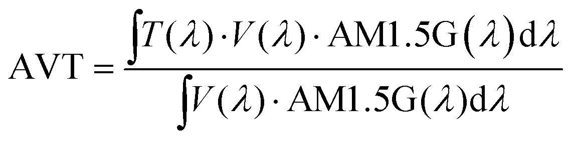
Fig. 1a and b depict the energy levels of the device structure and the corresponding SCAPS-1D-modeled band diagram. CuSCN layer functions as both electron blocking (because of its low conduction band energy level) and hole transport layers (because of its VB lying close to that of Sb2S3). The importance of appropriate processing of the CuSCN film to prepare a high-quality uniform film with optimum thickness has been described elsewhere.57,67–71 Based on these reports, the CuSCN film preparation conditions (spin speed, concentration, and drying conditions) were optimized to obtain a smooth and transparent film with a wide bandgap of ca. 3.85 eV (Fig. S3a and c, ESI†), consistent with the values reported elsewhere.54,72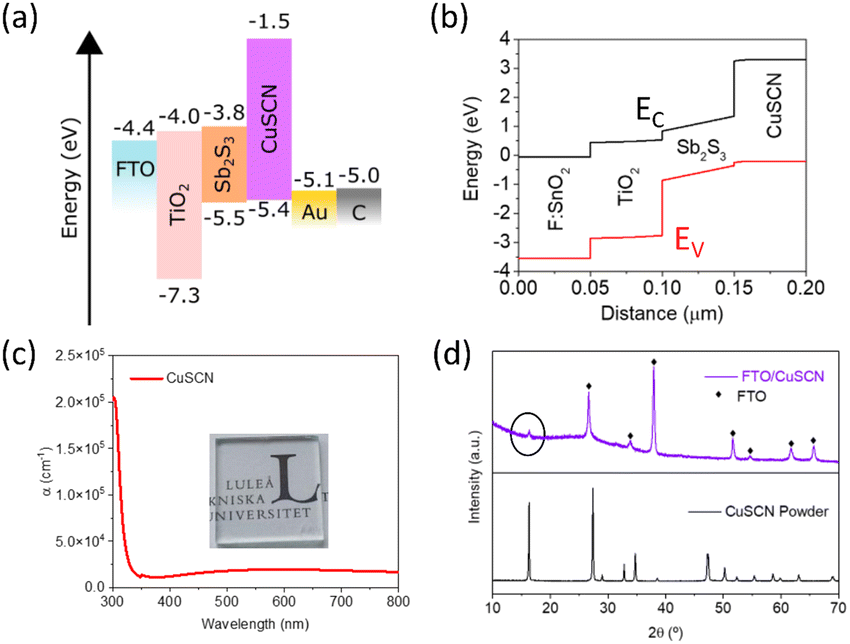 | ||
| Fig. 1 (a) The energy level diagram of each layer in the FTO/TiO2/Sb2S3/CuSCN/Au (or carbon) solar cells. (b) SCAPS-1D modeling determined energy band diagram of the solar cells at short circuit. (c) The absorption coefficient of a CuSCN thin film on a glass substrate. (d) X-Ray diffraction pattern of commercial CuSCN powder and the prepared CuSCN film on the FTO substrate. | ||
The absorption coefficient and photograph of a CuSCN film coated on glass are shown in Fig. 1c (in Fig. S3a, ESI,† the absorption coefficients of Sb2S3 and CuSCN are shown for comparison). The film appeared quite smooth after the optimized drying step. The XRD pattern of the CuSCN thin film and CuSCN powder (as received from Sigma-Aldrich) is shown in Fig. 1d. The peak located at 16.1° (003) is visible in ∼60 nm thin CuSCN, suggesting a crystalline β-CuSCN phase (while the powder spectrum matches too with the JCPDS #29-0581 standard for β-CuSCN).72
The top surface SEM image of the spin-coated CuSCN film on Sb2S3 (Fig. 2d) showed a full coverage of the island-like Sb2S3 layer (Fig. 2c), which would act as a good recombination barrier.33 The cross-section SEM images of the optimized Au- and C-electrode-based devices are shown in Fig. 2a and b, respectively, with an optimized CuSCN thickness of ∼60–70 nm—an optimum balance between the lowest resistance and full coverage film as evidenced in the photovoltaic performances of lower and higher RPMs in Fig. S1c and Table S3 (ESI†).73,74 Furthermore, to replace the vacuum-deposited Au electrode with a low-cost blade-coated carbon electrode, compatibility of the HTL with the solvent used in carbon paste was also verified. The CuSCN solid film was resistant to carbon paste solvent (mixture of acetone, 2-methoxy-1-methyl ethyl acetate, and xylene) as evident in the SEM image (Fig. S5a and b, ESI†) and absorption spectrum (Fig. S5c, ESI†) of the CuSCN surface without and with solvent treatment.
 | ||
| Fig. 2 Cross-section of Sb2S3 solar cells with CuSCN as the HTL with (a) an Au electrode and (b) a carbon electrode (a zoomed-out view is shown in Fig. S4, ESI†). SEM image of the top surface of (c) the annealed Sb2S3 film and (d) CuSCN deposited on top of the Sb2S3 film. | ||
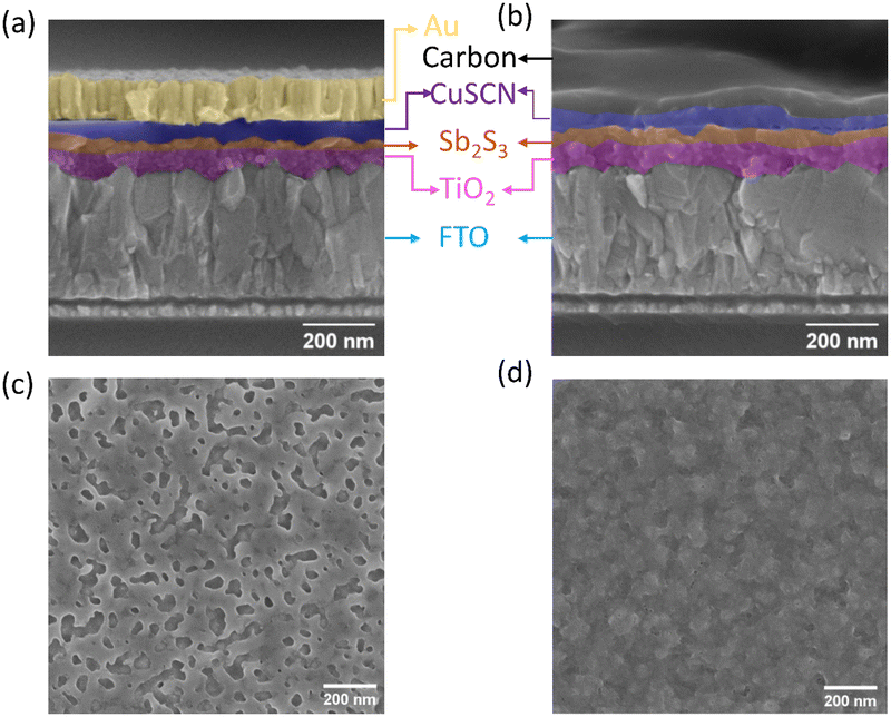
Table 1 lists the photovoltaic performance of Sb2S3 solar cells based on sputtered gold (Au-electrode) and carbon/Ag-paste electrode (C-electrode), and the corresponding device structures are shown in Fig. 2a and b. Fig. 3a shows the current density–voltage (J–V) curves for the champion devices, and the corresponding statistical analysis is shown in Fig. S6 (ESI†). A PCE of 1.95% (VOC = 0.611 V, JSC = 6.25 mA cm−2, and FF = 0.51) was obtained with a carbon electrode, while the device using the Au electrode exhibited a PCE of 1.75% with slightly improved JSC (7.10 mA cm−2) and lower VOC (0.501 V) and a similar FF (0.50). These PCEs are better than those reported in the literature for solution-processed planar Sb2S3 solar cells using CuSCN as the HTL with considerably improved VOC (see Table S5, ESI† for comparison with previous reports on planar CuSCN-based devices). For CBD deposited Sb2S3 devices with TiO2 as the ETL, the performance is at par with the PCE reported by Wang et al.31 (2.0%) and Lei et al. (1.9%)32 using organic spiro-OMeTAD and P3HT as the HTLs, respectively. The relatively low FFs of both these cells are also a result of the incomplete coverage of the TiO2 surface with the Sb2S3 ultrathin film (ca. ∼40–50 nm in Fig. 2c), which would induce a shunt path between the electron and hole transport layers (supported by shunted devices obtained with devices without the CuSCN layer, shown in Fig. S1c and Table S3, ESI†). Even with this highly porous active layer, little hysteresis was seen in the forward vs. reverse scan in the control device with the Au electrode, suggesting efficient charge transfer at the Sb2S3/HTL interface (Fig. S7, ESI†).
 | ||
| Fig. 3 (a) Light J–V curves and (b) external quantum efficiency of champion solar cells with Au and C electrodes, along with the reflectance spectrum of Au and C electrodes. (c) Corresponding dark J–V curves, used for the calculation of the device ideality factor (n) and reverse saturation current density (J0). (d) Linear J–V curve for FTO/CuSCN/electrode devices. | ||
Increasing the thickness of the Sb2S3 layer did not increase the JSC, and the performance was limited by all the parameters being low: lower JSC, VOC, and FF (see Fig. S1a and Table S1, ESI†). This observation agrees with the report by Zhang et al.75 In a previous report by Christians et al.,76 a similar planar device structure (FTO/TiO2/CBD-Sb2S3/CuSCN/Au) was studied to estimate the maximum Sb2S3 thickness of ∼50 nm to balance light absorption and charge extraction. Furthermore, in CBD deposited Sb2S3, impurity phases like Sb2O3 and Sb2(SO3)3 are inevitable since the reaction takes place in water.19,75 Since oxide impurities were not discernible from the XRD spectrum of a thin film of ∼90 nm (Fig. S3d, ESI†), a highly sensitive RBS measurement was carried out to analyze the composition of the CBD deposited Sb2S3 films (Fig. S8, ESI†). An optically active film has been deposited on the Si substrate for RBS analysis to avoid interference of heavy elements from FTO. The SbS film presents a homogeneous in-depth composition, with the presence of a significant amount of oxygen. The atomic composition of the film is Sb2.0S2.1O1.3, with a 24% atomic content of oxygen. Lian et al. used deep-level transient spectroscopy to study the defects in Sb2S3 with variations in composition.77 At smaller concentrations, oxygen impurities can passivate defects caused by S deficit, while excessive oxygen (like in the current analysis) would form detrimental OSb defects. Cai et al.78 used first-principles calculations to show that O can easily replace S in Sb2S3 (OS), leading to poor conductivity and a high hole-trap concentration. Surface treatments with a sulfur source have been suggested by Choi et al.23 to reduce the oxide phases, leading to as high as 29% improvement in photovoltaic performance. Hence, optimization of the active layer could be the focus of future studies focusing mainly on PCE improvements with the current device structure.
The short circuit current density, JSC, is influenced by the absorption and charge extraction properties of the solar cells. Comparatively, the lower JSC of the C-electrode device can be reasoned using the external quantum efficiency (EQE) and reflectance spectrum of electrodes (Fig. 3b). The integrated JSC values were in close agreement with the J–V curves (7.7 and 6.6 mA cm−2, for C and Au electrodes, respectively). The reflectance contribution in the EQE curve from the back electrode in the wavelength range of 600–700 nm is significantly higher for Au-solar cells (the internal quantum efficiency curve in Fig. S9 (ESI†) clearly shows that enhancement in the longer wavelength region). This observation has been reported elsewhere, using carbon electrodes.53 The carbon electrode reflects barely any light (<5% reflectance for all wavelengths in Fig. 3b). At the same time, an ultrathin Sb2S3 absorber layer cannot absorb all the light, especially the longer wavelengths (as can be seen in Fig. S3a (ESI†), the absorption coefficient of Sb2S3 drops steeply in the longer wavelength region). The Au electrode can reflect the unabsorbed transmitted light and contribute to higher EQE in the longer wavelength region and, hence, higher JSC. At the lower wavelength region where the reflectance from the Au electrode decreases sharply, lower EQE for Au electrode suggests that the photocurrent is dominated by drift current under the influence of a built-in electric field and charge extraction efficiency of the electrodes.79 The carbon electrode, thus, could collect holes more efficiently as the electron contacts are the same for both the devices. This is confirmed from the recombination resistance (Rrec) and built-in potential (Vbi) values calculated for the two devices in the subsequent analysis of the device.
Series and shunt resistances of the two devices in light were calculated from the linear region slopes near open circuit (Rs = dJ/dV|V=Voc) and short circuit (Rsh = dJ/dV|V=0V) conditions, respectively.80 The series resistance of the Au-device was slightly lower (8.15 Ω cm−2 for the Au-device vs. 8.6 Ω cm−2 for the C-device, calculated in the linear region near VOC). However, the shunt resistance for the Au device is much lower (505 Ω cm−2) compared to that of the C-device (636 Ω cm−2). A higher shunt resistance in the C-device means enhanced recombination resistance and higher FF and VOC.
Moreover, theoretically, VOC should be independent of the electrode since it depends on the quasi-Fermi level energy splitting between the ETL and the HTL in n-i-p solar cells.81–83 Also, given that the WF of C and Au is similar (−5.0 and −5.1 eV, respectively),53 the VOC values are expected to be similar.84 The reason for increased VOC (statistics of variation in performance parameters among devices is shown in Fig. S6, ESI†) of the C-electrode solar cell was studied in detail since it is the major limitation in Sb2(S,Se)3 solar cells.85Voc depends on the diode ideality factor, n, and saturation current density, J0 as:
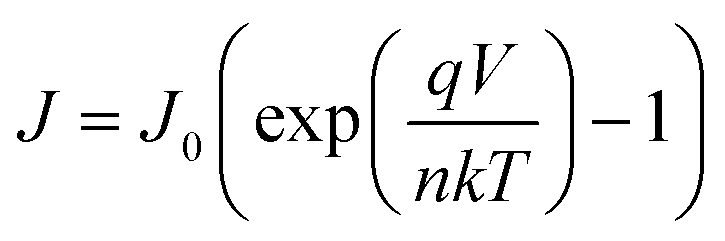
The ideality factor of the C-electrode solar cell (n = 1.68) is lower than that of the Au-electrode solar cell (n = 2.19). Since the HTL and ETL are the same for the devices and VOC was significantly different, the ideality factor values represent both bulk recombination and surface recombination at the contacts.88J0 decreased by almost three orders of magnitude from 1.1 × 10⁻⁴ to 6.4 × 10⁻⁷ mA cm−2 using a C electrode vs. Au electrode. Both these values suggest reduced recombination (contact interface and bulk) and thus higher VOC and FF for C-based devices.89 Higher leakage currents also suggest a comparatively higher shunting in the Au device (the rectification ratio of dark currents at ±1 V was ca. 14350 for C electrode and 287 for Au electrode). This shunting behavior complicates the direct comparison between these devices based only on dark IV analysis.90
It is also noteworthy that both electrodes form a near-Ohmic contact with the CuSCN layer (Fig. 3d). Therefore, the VOC discrepancy does not seem to originate from energy level offsets (leading to an injection barrier) between the electrode and HTL.83 It is likely that the physical contact between carbon and CuSCN is more passivating in nature as compared to the Au electrode, indicating less surface recombination at contacts. Notably, the CuSCN surface did not show a visible change with the solvent used in the C paste because of the limited solubility of CuSCN in common solvents such as xylene (Fig. S5a–c, ESI†).91
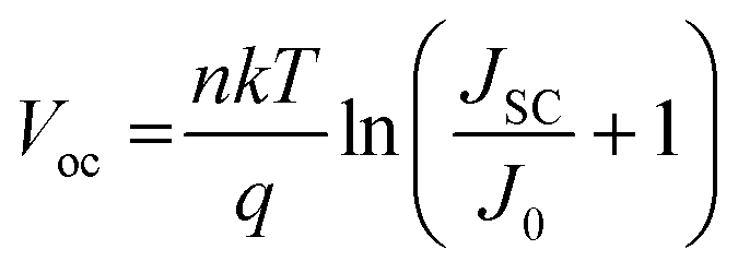
Furthermore, interface and charge transport characteristics of the cells with Au and C/Ag back-contact were studied using electrochemical impedance spectroscopy measurements (EIS) in the dark at an applied voltage of 0.5 V (close to VOC). The Nyquist plot showed a single depressed semicircle which is modeled by a series resistance component, RS,EIS (combining all resistances including that of electrodes) in series with a parallel combination of recombination resistance (Rrec)—constant phase element (CPE). The Rs,EIS value for Au-device is slightly lower because of the reduced resistance of the Au electrode, while the Rrec for C-device is substantially higher (Table S6, ESI†). High Rrec implies reduced recombination in the C-device, thus higher VOC. Since the TiO2/Sb2S3 and Sb2S3/CuSCN interfaces are identical and WFs of electrodes are similar in both cases, the Rrec values are primarily associated with the CuSCN/electrode interfaces. This observation is consistent with the reports where C-electrode has been reported to possess both HTL and charge collection properties.92–94
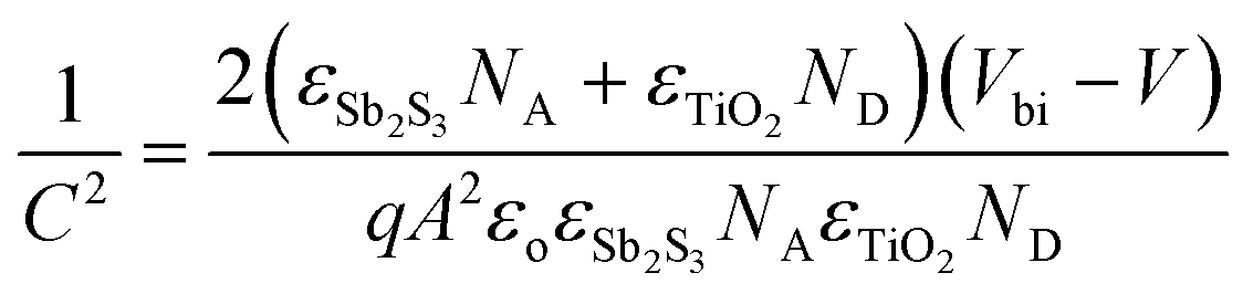
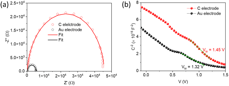
Capacitance–voltage (C–V) measurements were carried out to study the carrier accumulation and transport properties at the interface.95,96 Capacitance response in these measurements corresponds to free carriers along with bulk and interfacial defects.97 For the devices studied here, the differences in the capacitance response would arise from different charge extraction properties of the contacts. Fig. 4b shows Mott–Schottky (M–S) plots of devices with the two electrodes at 10 kHz in the dark. It shows a bias-dependent capacitance demonstrating the presence of an abrupt p–n+ (Sb2S3/TiO2) junction, where TiO2 is a highly doped n-type material (calculated ND = 2.4 × 1019 cm−3, and the corresponding Mott–Schottky analysis shown in Fig. S10, ESI†).98,99 The charge carrier (acceptor) concentration (NA) at the edge of the p-side depletion region and total build-in potential (Vbi) were calculated using the following equation:
 | ||
| Fig. 4 Nyquist plots (a) and Mott–Schottky with fitted line plots (b) for C and Au-based solar cell devices. | ||
Since the electron transport and collection side are the same for both devices, the calculated parameters mentioned above point to an inefficient charge collection and possible shunt at the CuSCN/Au interface. The blade-coated carbon electrode with large graphite flakes (Fig. S4, ESI†) is less prone to shunting than the vacuum deposited Au electrode and makes intimate contact with the CuSCN layer. This is supported by the peel-off test using a strong copper adhesive tape. The Au electrode was peeled off while the carbon electrode remained intact, suggesting intimate contact with the underlying CuSCN layer (Fig. S12, ESI†). A similar observation has been reported by Aung et al.105
The high transparency of CuSCN thin films (with a wide bandgap of 3.85 eV) and an extremely thin Sb2S3 absorber layer enable a semitransparent solar cell. A high AVT of ∼27.5% for the complete device (for the device without top electrode AVT = 39.1% vs. air was calculated) and a PCE of 1.67% (VOC = 0.560 V, JSC = 6.12 mA cm−2, and FF = 0.49) were obtained with the same structure as that of opaque Au electrode-based solar cells, except that the electrode thickness was reduced to ∼15 nm (Fig. 5a and b). Further optimization is needed to achieve the highest light utilization efficiency (LUE = PCE × AVT) since PCE and AVT are mostly inversely related. For example, a solution-processed carbon-based transparent top electrode such as graphene could replace the vacuum-processed ultrathin Au electrode.106 However, this report focuses on the viability of a semitransparent Sb2S3 solar cell using this combination of inorganic electron (TiO2) and hole (CuSCN) transport layers. Further optimization of the absorber layer composition and morphology would be carried out using different deposition methods and post-deposition treatments to reduce the amount of oxygen impurities,23 obtain larger grains,107 and achieve preferential [hk1] orientation17,108–111 of Sb2S3 crystallites (compared to predominantly [hk0] in the obtained thin film shown in Fig. S3d, ESI†). Also, a stability study in comparison to the organic HTL layer would be carried out to illustrate the inherent stability of the device layer vs. the stability of the completed device.
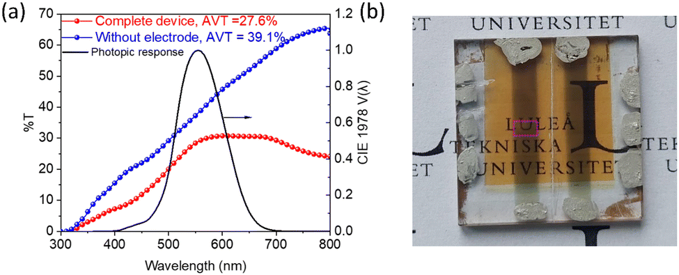 | ||
| Fig. 5 (a) Transmission spectrum of the semitransparent device with and without a top electrode (∼15 nm Au), along with the human eye's photopic response. (b) Photograph of a semitransparent device with the active area marked using a pink dotted rectangle. | ||
Conclusions
In summary, a compact CuSCN layer deposited via spin coating under ambient conditions suppressed the shunt paths in the chemical bath deposited Sb2S3 solar cells implementing a simple planar configuration—FTO/TiO2/Sb2S3/CuSCN/Au or C/Ag. The robust CuSCN layer showed good interfacial contact with the carbon electrode resulting in even improved solar cell performance compared to the vacuum-deposited Au electrode, achieving a PCE of 1.95%. A higher VOC in carbon-based devices is attributed to better diode characteristics, high recombination resistance, and a higher Vbi. Enhancing VOC using an improved CuSCN/electrode interface is a promising direction for future studies since a significant limitation in the performance of Sb2S3 solar cells stems from voltage loss (>50% lower than the SQ limit of 1.4 V).85 Moreover, the high transparency and smoothness of the CuSCN layer allowed achieving a preliminary semitransparent solar device with an impressive AVT of 26.7% with a PCE of 1.67%. The lower overall PCE, though, is reflective of a low-quality CBD deposited absorber layer with high amounts of oxygen impurities and unfavorable (hk0) orientation, which can be overcome by alternate deposition methods like rapid thermal evaporation, vapor transport deposition, ALD, and so on.11 Overall, the focus of this study was to demonstrate the compatibility and potential of CuSCN as the HTL in Sb2S3 (or potentially in Sb2Se3 because of a similar crystal structure) solar cell devices using carbon electrodes and semitransparent solar cell devices.Author contributions
P. K.: conceptualization, methodology, investigation, writing original draft, and formal analysis. S. Y.: supervision and review. A. V.: supervision, review and editing.Conflicts of interest
There are no conflicts to declare.Acknowledgements
A. V. acknowledges the Knut & Alice Wallenberg Foundation and the Kempe Foundation for financial support.References
- O. Almora, D. Baran, G. C. Bazan, C. Berger, C. I. Cabrera, K. R. Catchpole, S. Erten-Ela, F. Guo, J. Hauch, A. W. Y. Ho-Baillie, T. J. Jacobsson, R. A. J. Janssen, T. Kirchartz, N. Kopidakis, Y. Li, M. A. Loi, R. R. Lunt, X. Mathew, M. D. McGehee, J. Min, D. B. Mitzi, M. K. Nazeeruddin, J. Nelson, A. F. Nogueira, U. W. Paetzold, N.-G. Park, B. P. Rand, U. Rau, H. J. Snaith, E. Unger, L. Vaillant-Roca, H.-L. Yip and C. J. Brabec, Adv. Energy Mater., 2021, 11, 2102526 CrossRef CAS.
- A. Zakutayev, J. D. Major, X. Hao, A. Walsh, J. Tang, T. K. Todorov, L. H. Wong and E. Saucedo, J. Phys. Energy, 2021, 3, 032003 CrossRef CAS.
- Y. Sun, H. Xu, Y. Kan and K. Gao, Sci. China Mater., 2022, 65, 2609–2610 CrossRef CAS.
- Y. Sun, R. Ma, Y. Kan, T. Liu, K. Zhou, P. Liu, J. Fang, Y. Chen, L. Ye, C. Ma, H. Yan and K. Gao, Macromol. Rapid Commun., 2022, 2200139 CrossRef PubMed.
- R. Ma, K. Zhou, Y. Sun, T. Liu, Y. Kan, Y. Xiao, T. A. Dela Peña, Y. Li, X. Zou, Z. Xing, Z. Luo, K. S. Wong, X. Lu, L. Ye, H. Yan and K. Gao, Matter, 2022, 5, 725–734 CrossRef CAS.
- M. He, C. Yan, J. Li, M. P. Suryawanshi, J. Kim, M. A. Green and X. Hao, Adv. Sci., 2021, 8, 2004313 CrossRef CAS PubMed.
- O. Almora, D. Baran, G. C. Bazan, C. Berger, C. I. Cabrera, K. R. Catchpole, S. Erten-Ela, F. Guo, J. Hauch, A. W. Y. Ho-Baillie, T. J. Jacobsson, R. A. J. Janssen, T. Kirchartz, N. Kopidakis, Y. Li, M. A. Loi, R. R. Lunt, X. Mathew, M. D. McGehee, J. Min, D. B. Mitzi, M. K. Nazeeruddin, J. Nelson, A. F. Nogueira, U. W. Paetzold, N.-G. Park, B. P. Rand, U. Rau, H. J. Snaith, E. Unger, L. Vaillant-Roca, H.-L. Yip and C. J. Brabec, Adv. Energy Mater., 2021, 11, 2002774 CrossRef CAS.
- L. H. Wong, A. Zakutayev, J. D. Major, X. Hao, A. Walsh, T. K. Todorov and E. Saucedo, J. Phys. Energy, 2019, 1, 032001 CrossRef CAS.
- R. Nie, M. Hu, A. M. Risqi, Z. Li and S. I. Seok, Adv. Sci., 2021, 8, 2003172 CrossRef CAS PubMed.
- S. Rühle, Sol. Energy, 2016, 130, 139–147 CrossRef.
- Q. Wang, Z. Chen, J. Wang, Y. Xu, Y. Wei, Y. Wei, L. Qiu, H. Lu, Y. Ding and J. Zhu, Inorg. Chem. Front., 2019, 6, 3381–3397 RSC.
- M. Y. Versavel and J. A. Haber, Thin Solid Films, 2007, 515, 7171–7176 CrossRef CAS.
- X. Wang, Z. Li, S. R. Kavanagh, A. M. Ganose and A. Walsh, Phys. Chem. Chem. Phys., 2022, 24, 7195–7202 RSC.
- H. Deng, Y. Zeng, M. Ishaq, S. Yuan, H. Zhang, X. Yang, M. Hou, U. Farooq, J. Huang, K. Sun, R. Webster, H. Wu, Z. Chen, F. Yi, H. Song, X. Hao and J. Tang, Adv. Funct. Mater., 2019, 29, 1901720 CrossRef.
- Z. Yang, X. Wang, Y. Chen, Z. Zheng, Z. Chen, W. Xu, W. Liu, Y. (Michael) Yang, J. Zhao, T. Chen and H. Zhu, Nat. Commun., 2019, 10, 4540 CrossRef PubMed.
- R. Kondrotas, C. Chen and J. Tang, Joule, 2018, 2, 857–878 CrossRef CAS.
- X. Jin, Y. Fang, T. Salim, M. Feng, S. Hadke, S. W. Leow, T. C. Sum and L. H. Wong, Adv. Funct. Mater., 2020, 30, 2002887 CrossRef CAS.
- U. A. Shah, S. Chen, G. M. G. Khalaf, Z. Jin and H. Song, Adv. Funct. Mater., 2021, 31, 2100265 CrossRef CAS.
- A. Darga, D. Mencaraglia, C. Longeaud, T. J. Savenije, B. O’Regan, S. Bourdais, T. Muto, B. Delatouche and G. Dennler, J. Phys. Chem. C, 2013, 117, 20525–20530 CrossRef CAS.
- R. Tang, X. Wang, C. Jiang, S. Li, W. Liu, H. Ju, S. Yang, C. Zhu and T. Chen, ACS Appl. Mater. Interfaces, 2018, 10, 30314–30321 CrossRef CAS PubMed.
- P. P. Boix, Y. H. Lee, F. Fabregat-Santiago, S. H. Im, I. Mora-Sero, J. Bisquert and S. I. Seok, ACS Nano, 2012, 6, 873–880 CrossRef CAS PubMed.
- J. Han, S. Wang, J. Yang, S. Guo, Q. Cao, H. Tang, X. Pu, B. Gao and X. Li, ACS Appl. Mater. Interfaces, 2020, 12, 4970–4979 CrossRef CAS PubMed.
- Y. C. Choi, D. U. Lee, J. H. Noh, E. K. Kim and S. I. Seok, Adv. Funct. Mater., 2014, 24, 3587–3592 CrossRef CAS.
- S.-J. Lee, S.-J. Sung, K.-J. Yang, J.-K. Kang, J. Y. Kim, Y. S. Do and D.-H. Kim, ACS Appl. Energy Mater., 2020, 3, 12644–12651 CrossRef CAS.
- J. S. Eensalu, A. Katerski, E. Kärber, L. Weinhardt, M. Blum, C. Heske, W. Yang, I. Oja Acik and M. Krunks, Beilstein J. Nanotechnol., 2019, 10, 2396–2409 CrossRef CAS PubMed.
- L. Zhang, C. Jiang, C. Wu, H. Ju, G. Jiang, W. Liu, C. Zhu and T. Chen, ACS Appl. Mater. Interfaces, 2018, 10, 27098–27105 CrossRef CAS PubMed.
- J. Zhang, W. Lian, Y. Yin, X. Wang, R. Tang, C. Qian, X. Hao, C. Zhu and T. Chen, Sol. RRL, 2020, 4, 2000048 CrossRef CAS.
- E. Zimmermann, T. Pfadler, J. Kalb, J. A. Dorman, D. Sommer, G. Hahn, J. Weickert and L. Schmidt-Mende, Adv. Sci., 2015, 2, 1500059 CrossRef PubMed.
- X. Wang, R. Tang, C. Wu, C. Zhu and T. Chen, J. Energy Chem., 2018, 27, 713–721 CrossRef.
- T. Englman, E. Terkieltaub and L. Etgar, J. Phys. Chem. C, 2015, 119, 12904–12909 CrossRef CAS.
- X. Wang, J. Li, W. Liu, S. Yang, C. Zhu and T. Chen, Nanoscale, 2017, 9, 3386–3390 RSC.
- H. Lei, G. Yang, Y. Guo, L. Xiong, P. Qin, X. Dai, X. Zheng, W. Ke, H. Tao, Z. Chen, B. Li and G. Fang, Phys. Chem. Chem. Phys., 2016, 18, 16436–16443 RSC.
- Y. O. Mayon, T. P. White, R. Wang, Z. Yang and K. R. Catchpole, Phys. Status Solidi A, 2016, 213, 108–113 CrossRef.
- N. Wijeyasinghe, A. Regoutz, F. Eisner, T. Du, L. Tsetseris, Y.-H. Lin, H. Faber, P. Pattanasattayavong, J. Li, F. Yan, M. A. McLachlan, D. J. Payne, M. Heeney and T. D. Anthopoulos, Adv. Funct. Mater., 2017, 27, 1701818 CrossRef.
- R. Singh, P. K. Singh, B. Bhattacharya and H.-W. Rhee, Appl. Mater. Today, 2019, 14, 175–200 CrossRef.
- K. Li, S. Wang, C. Chen, R. Kondrotas, M. Hu, S. Lu, C. Wang, W. Chen and J. Tang, J. Mater. Chem. A, 2019, 7, 9665–9672 RSC.
- H. Deng, S. Chen, M. Ishaq, Y. Cheng, Q. Sun, X. Lin, Q. Zheng, C. Zhang and S. Cheng, Sol. RRL, 2022, 6, 2101017 CrossRef CAS.
- M. Ishaq, H. Deng, U. Farooq, H. Zhang, X. Yang, U. A. Shah and H. Song, Sol. RRL, 2019, 3, 1900305 CrossRef CAS.
- Y. Itzhaik, O. Niitsoo, M. Page and G. Hodes, J. Phys. Chem. C, 2009, 113, 4254–4256 CrossRef CAS.
- K. Tsujimoto, D.-C. Nguyen, S. Ito, H. Nishino, H. Matsuyoshi, A. Konno, G. R. A. Kumara and K. Tennakone, J. Phys. Chem. C, 2012, 116, 13465–13471 CrossRef CAS.
- S. Ito, K. Tsujimoto, D.-C. Nguyen, K. Manabe and H. Nishino, Int. J. Hydrogen Energy, 2013, 38, 16749–16754 CrossRef CAS.
- T. Muto, G. Larramona and G. Dennler, Appl. Phys. Express, 2013, 6, 072301 CrossRef.
- Y. Zhao, P. Cheng, H. Yang, M. Wang, D. Meng, Y. Zhu, R. Zheng, T. Li, A. Zhang, S. Tan, T. Huang, J. Bian, X. Zhan, P. S. Weiss and Y. Yang, ACS Nano, 2022, 16, 1231–1238 CrossRef CAS PubMed.
- P. Cheng, H.-C. Wang, Y. Zhu, R. Zheng, T. Li, C.-H. Chen, T. Huang, Y. Zhao, R. Wang, D. Meng, Y. Li, C. Zhu, K.-H. Wei, X. Zhan and Y. Yang, Adv. Mater., 2020, 32, 2003891 CrossRef CAS PubMed.
- Y. Liu, P. Cheng, T. Li, R. Wang, Y. Li, S.-Y. Chang, Y. Zhu, H.-W. Cheng, K.-H. Wei, X. Zhan, B. Sun and Y. Yang, ACS Nano, 2019, 13, 1071–1077 CrossRef CAS PubMed.
- J. Sun and J. J. Jasieniak, J. Phys. Appl. Phys., 2017, 50, 093001 CrossRef.
- A. A. F. Husain, W. Z. W. Hasan, S. Shafie, M. N. Hamidon and S. S. Pandey, Renewable Sustainable Energy Rev., 2018, 94, 779–791 CrossRef CAS.
- M. Saifullah, J. Gwak and J. H. Yun, J. Mater. Chem. A, 2016, 4, 8512–8540 RSC.
- Z. Chen and G. Chen, Sol. Energy, 2020, 201, 323–329 CrossRef CAS.
- R. Tang, X. Wang, W. Lian, J. Huang, Q. Wei, M. Huang, Y. Yin, C. Jiang, S. Yang, G. Xing, S. Chen, C. Zhu, X. Hao, M. A. Green and T. Chen, Nat. Energy, 2020, 5, 587–595 CrossRef CAS.
- J. Han, X. Pu, H. Zhou, Q. Cao, S. Wang, Z. He, B. Gao, T. Li, J. Zhao and X. Li, ACS Appl. Mater. Interfaces, 2020, 12, 44297–44306 CrossRef CAS PubMed.
- C. Jiang, R. Tang, X. Wang, H. Ju, G. Chen and T. Chen, Sol. RRL, 2019, 3, 1800272 CrossRef.
- G. A. Sepalage, H. Weerasinghe, N. Rai, N. W. Duffy, S. R. Raga, Y. Hora, M. Gao, D. Vak, A. S. R. Chesman, U. Bach and A. N. Simonov, Adv. Mater. Technol., 2022, 7, 2101148 CrossRef CAS.
- N. Wijeyasinghe, F. Eisner, L. Tsetseris, Y.-H. Lin, A. Seitkhan, J. Li, F. Yan, O. Solomeshch, N. Tessler, P. Patsalas and T. D. Anthopoulos, Adv. Funct. Mater., 2018, 28, 1802055 CrossRef.
- J. Peng, F. Kremer, D. Walter, Y. Wu, Y. Ji, J. Xiang, W. Liu, T. Duong, H. Shen, T. Lu, F. Brink, D. Zhong, L. Li, O. Lee Cheong Lem, Y. Liu, K. J. Weber, T. P. White and K. R. Catchpole, Nature, 2022, 601, 573–578 CrossRef CAS PubMed.
- S. Messina, M. T. S. Nair and P. K. Nair, Thin Solid Films, 2007, 515, 5777–5782 CrossRef CAS.
- J. W. Jung, C.-C. Chueh and A. K.-Y. Jen, Adv. Energy Mater., 2015, 5, 1500486 CrossRef.
- C. Chen, W. Li, Y. Zhou, C. Chen, M. Luo, X. Liu, K. Zeng, B. Yang, C. Zhang, J. Han and J. Tang, Appl. Phys. Lett., 2015, 107, 043905 CrossRef.
- Y. Li, W. Yan, Y. Li, S. Wang, W. Wang, Z. Bian, L. Xiao and Q. Gong, Sci. Rep., 2015, 5, 14485 CrossRef CAS PubMed.
- E. Cárdenas, A. Arato, E. Perez-Tijerina, T. K. Das Roy, G. Alan Castillo and B. Krishnan, Sol. Energy Mater. Sol. Cells, 2009, 93, 33–36 CrossRef.
- L. Guo, B. Zhang, S. Li, Q. Zhang, M. Buettner, L. Li, X. Qian and F. Yan, APL Mater., 2019, 7, 041105 CrossRef.
- X.-D. Gao, X.-M. Li, W.-D. Yu, J.-J. Qiu and X.-Y. Gan, Thin Solid Films, 2008, 517, 554–559 CrossRef CAS.
- B. R. Sankapal, E. Goncalves, A. Ennaoui and M. C. Lux-Steiner, Thin Solid Films, 2004, 451–452, 128–132 CrossRef CAS.
- K. Lee, H.-D. Um, D. Choi, J. Park, N. Kim, H. Kim and K. Seo, Cell Rep. Phys. Sci., 2020, 1, 100143 CrossRef CAS.
- A. S. Bondarenko and G. A. Ragoisha, Nova Sci., New York, http://https//www.abc.chemistry.bsu.by/vi/, 2005, 1110–1112 Search PubMed.
- M. Burgelman, P. Nollet and S. Degrave, Thin Solid Films, 2000, 361–362, 527–532 CrossRef CAS.
- I. S. Yang, M. R. Sohn, S. D. Sung, Y. J. Kim, Y. J. Yoo, J. Kim and W. I. Lee, Nano Energy, 2017, 32, 414–421 CrossRef CAS.
- S. Ito, S. Tanaka and H. Nishino, J. Phys. Chem. Lett., 2015, 6, 881–886 CrossRef CAS PubMed.
- S. Chavhan, O. Miguel, H.-J. Grande, V. Gonzalez-Pedro, R. S. Sánchez, E. M. Barea, I. Mora-Seró and R. Tena-Zaera, J. Mater. Chem. A, 2014, 2, 12754–12760 RSC.
- L. Fan, Y. Li, X. Yao, Y. Ding, S. Zhao, B. Shi, C. Wei, D. Zhang, B. Li, G. Wang, Y. Zhao and X. Zhang, ACS Appl. Energy Mater., 2018, 1, 1575–1584 CrossRef CAS.
- A. Montgomery, L. Guo, C. Grice, R. A. Awni, S. Saurav, L. Li, Y. Yan and F. Yan, Prog. Photovolt.: Res. Appl., 2019, 27, 665–672 CAS.
- M. Jung, Y. C. Kim, N. J. Jeon, W. S. Yang, J. Seo, J. H. Noh and S. Il Seok, ChemSusChem, 2016, 9, 2592–2596 CrossRef CAS PubMed.
- S. Ye, W. Sun, Y. Li, W. Yan, H. Peng, Z. Bian, Z. Liu and C. Huang, Nano Lett., 2015, 15, 3723–3728 CrossRef CAS PubMed.
- N. Arora, M. I. Dar, A. Hinderhofer, N. Pellet, F. Schreiber, S. M. Zakeeruddin and M. Grätzel, Science, 2017, 358, 768–771 CrossRef CAS PubMed.
- X. Zhang, S. Yoshioka, N. Loew and M. Ihara, ECS Trans., 2014, 64, 1 CrossRef CAS.
- J. A. Christians, D. T. Leighton and P. V. Kamat, Energy Environ. Sci., 2014, 7, 1148–1158 RSC.
- W. Lian, C. Jiang, Y. Yin, R. Tang, G. Li, L. Zhang, B. Che and T. Chen, Nat. Commun., 2021, 12, 3260 CrossRef CAS PubMed.
- Z. Cai, C.-M. Dai and S. Chen, Sol. RRL, 2020, 4, 1900503 CrossRef CAS.
- M.-J. Choi, S. Kim, H. Lim, J. Choi, D. M. Sim, S. Yim, B. T. Ahn, J. Y. Kim and Y. S. Jung, Adv. Mater., 2016, 28, 1780–1787 CrossRef CAS PubMed.
- D. S. H. Chan and J. C. H. Phang, IEEE Trans. Electron Devices, 1987, 34, 286–293 Search PubMed.
- K. Shen, Y. Zhang, X. Wang, C. Ou, F. Guo, H. Zhu, C. Liu, Y. Gao, R. E. I. Schropp, Z. Li, X. Liu and Y. Mai, Adv. Sci., 2020, 7, 2001013 CrossRef CAS PubMed.
- C. Chen, L. Wang, L. Gao, D. Nam, D. Li, K. Li, Y. Zhao, C. Ge, H. Cheong, H. Liu, H. Song and J. Tang, ACS Energy Lett., 2017, 2, 2125–2132 CrossRef CAS.
- P. R. Brown, R. R. Lunt, N. Zhao, T. P. Osedach, D. D. Wanger, L.-Y. Chang, M. G. Bawendi and V. Bulović, Nano Lett., 2011, 11, 2955–2961 CrossRef CAS PubMed.
- P. Mariani, L. Najafi, G. Bianca, M. I. Zappia, L. Gabatel, A. Agresti, S. Pescetelli, A. Di Carlo, S. Bellani and F. Bonaccorso, ACS Appl. Mater. Interfaces, 2021, 13, 22368–22380 CrossRef CAS PubMed.
- J. Dong, Y. Liu, Z. Wang and Y. Zhang, Nano Sel., 2021, 2, 1818–1848 CrossRef CAS.
- V. Nadenau, U. Rau, A. Jasenek and H. W. Schock, J. Appl. Phys., 2000, 87, 584–593 CrossRef CAS.
- J. R. Sites and P. H. Mauk, Sol. Cells, 1989, 27, 411–417 CrossRef CAS.
- O. J. Sandberg, A. Sundqvist, M. Nyman and R. Österbacka, Phys. Rev. Appl., 2016, 5, 044005 CrossRef.
- S. Yuan, H. Deng, X. Yang, C. Hu, J. Khan, W. Ye, J. Tang and H. Song, ACS Photonics, 2017, 4, 2862–2870 CrossRef CAS.
- T. Kirchartz, F. Deledalle, P. S. Tuladhar, J. R. Durrant and J. Nelson, J. Phys. Chem. Lett., 2013, 4, 2371–2376 CrossRef CAS.
- N. Chaudhary, R. Chaudhary, J. P. Kesari and A. Patra, Opt. Mater., 2017, 69, 367–371 CrossRef CAS.
- W. Chen, L. Jiang, R. Pathak and F. Wu, ECS J. Solid State Sci. Technol., 2019, 8, Q67 CrossRef CAS.
- E. Calabrò, F. Matteocci, B. Paci, L. Cinà, L. Vesce, J. Barichello, A. Generosi, A. Reale and A. Di Carlo, ACS Appl. Mater. Interfaces, 2020, 12, 32536–32547 CrossRef PubMed.
- H. Zhou, Y. Shi, Q. Dong, H. Zhang, Y. Xing, K. Wang, Y. Du and T. Ma, J. Phys. Chem. Lett., 2014, 5, 3241–3246 CrossRef CAS PubMed.
- U. K. Thakur, P. Kumar, S. Gusarov, A. E. Kobryn, S. Riddell, A. Goswami, K. M. Alam, S. Savela, P. Kar, T. Thundat, A. Meldrum and K. Shankar, ACS Appl. Mater. Interfaces, 2020, 12, 11467–11478 CrossRef CAS PubMed.
- E. von Hauff, J. Phys. Chem. C, 2019, 123, 11329–11346 CrossRef CAS.
- W. Wang, X. Wang, G. Chen, L. Yao, X. Huang, T. Chen, C. Zhu, S. Chen, Z. Huang and Y. Zhang, Adv. Electron. Mater., 2019, 5, 1800683 CrossRef.
- S. M. Willis, C. Cheng, H. E. Assender and A. A. R. Watt, Nano Lett., 2012, 12, 1522–1526 CrossRef CAS PubMed.
- A. Mani, C. Huisman, A. Goossens and J. Schoonman, J. Phys. Chem. B, 2008, 112, 10086–10091 CrossRef CAS PubMed.
- M. T. Islam and A. K. Thakur, Sol. Energy, 2020, 202, 304–315 CrossRef CAS.
- L. Kavan, N. Tétreault, T. Moehl and M. Grätzel, J. Phys. Chem. C, 2014, 118, 16408–16418 CrossRef CAS.
- D. A. Neamen, Semiconductor physics and devices: basic principles, McGraw-Hill; New York, NY, 4th edn, 2012 Search PubMed.
- M. Burgelman and P. Nollet, Solid State Ionics, 2005, 176, 2171–2175 CrossRef CAS.
- O. Almora, I. Zarazua, E. Mas-Marza, I. Mora-Sero, J. Bisquert and G. Garcia-Belmonte, J. Phys. Chem. Lett., 2015, 6, 1645–1652 CrossRef CAS PubMed.
- S. K. K. Aung, A. Vijayan, T. Seetawan and G. Boschloo, Sol. RRL, 2022, 6, 2100773 CrossRef CAS.
- Y. Sun, T. Liu, Y. Kan, K. Gao, B. Tang and Y. Li, Small Sci., 2021, 1, 2100001 CrossRef CAS.
- U. Chalapathi, B. Poornaprakash, C.-H. Ahn and S.-H. Park, Mater. Sci. Semicond. Process., 2018, 84, 138–143 CrossRef CAS.
- Y. Zeng, K. Sun, J. Huang, M. P. Nielsen, F. Ji, C. Sha, S. Yuan, X. Zhang, C. Yan, X. Liu, H. Deng, Y. Lai, J. Seidel, N. Ekins-Daukes, F. Liu, H. Song, M. Green and X. Hao, ACS Appl. Mater. Interfaces, 2020, 12, 22825–22834 CrossRef CAS PubMed.
- L. Liu, S.-L. Zhang, J.-Y. Wu, W.-H. Wang, W. Liu, L. Wu and Y. Zhang, Chin. Phys. B, 2020, 29, 058801 CrossRef CAS.
- F. Li, C. Wang, P. Liu, Y. Xiao, L. Bai, F. Qi, X. Hou, H. Zhang, Y. Wang, S. Wang and X.-Z. Zhao, Sol. RRL, 2019, 3, 1800297 CrossRef.
- J. Chen, J. Qi, R. Liu, X. Zhu, Z. Wan, Q. Zhao, S. Tao, C. Dong, G. Y. Ashebir, W. Chen, R. Peng, F. Zhang, S. Yang, X. Tian and M. Wang, Commun. Chem., 2019, 2, 1–9 CrossRef.
Footnote |
| † Electronic supplementary information (ESI) available. See DOI: https://doi.org/10.1039/d2tc03420d |
| This journal is © The Royal Society of Chemistry 2022 |