
 Open Access Article
 This Open Access Article is licensed under a
 Creative Commons Attribution 3.0 Unported Licence
Nitrogen stabilizes the wurtzite polymorph in ZnSe1−xTex thin films
Theodore H.
Culman
 a,
Rachel
Woods-Robinson
b,
John S.
Mangum
a,
Rebecca W.
Smaha
a,
Christopher L.
Rom
a,
Andriy
Zakutayev
a and
Sage R.
Bauers
*a
a,
Rachel
Woods-Robinson
b,
John S.
Mangum
a,
Rebecca W.
Smaha
a,
Christopher L.
Rom
a,
Andriy
Zakutayev
a and
Sage R.
Bauers
*a
aNational Renewable Energy Laboratory, Golden, CO, USA. E-mail: sage.bauers@nrel.gov
bLawrence Berkeley National Laboratory, Berkeley, CA, USA
First published on 5th October 2022
Abstract
Materials based on tetrahedral structural motifs are the most used semiconductor systems in deployed technologies. This holds true for microelectronics based on doped Si (diamond structure), photovoltaics based on CdTe (zinc blende structure), and light emitting diodes based on GaN (wurtzite structure). In these compound examples, the extended crystal structure is determined by modifications to the arrangement of the underlying tetrahedral motifs; controlling this structure is a foundational way to design functionality in semiconductor materials. Here, N-doped ZnSe1−xTex thin films are grown by RF sputtering from compound targets with N2 gas as a N source. Crystalline films form across a large range of growth conditions, and in some N-doped films there is a transformation from the usual zinc blende structure to wurtzite. Depending on the temperature and N2 flow rate during growth, wurtzite can be synthesized across most of the composition range explored, ranging from Te-rich (x ≈ 0.7) to nearly pure ZnSe (x ≈ 0.1). Synchrotron diffraction data show that the wurtzite is phase-pure at N-doped ZnSe0.5Te0.5 alloy compositions grown under some conditions. Temperature-dependent resistivity measurements collected from N-doped ZnSe0.5Te0.5 are well fit by a model dominated by variable range hopping, suggesting defect-mediated transport. Density functional theory calculations that show that dilute N concentrations help stabilize the wurtzite polymorph of ZnSe0.5Te0.5. Electron microscopy reveals voids in the N-doped films’ microstructures. We attribute this more open microstructure—which may also be partially responsible for stabilizing the wurtzite phase—to trapped N2. This work highlights unexpected polytypism in one of the most studied semiconductor systems, motivating a closer look at other semiconductor alloys for similar structural diversity.
Introduction
Zinc blende (ZB) and wurtzite (WZ) are the most common semiconductor crystal structures for multi-element compounds and are stacking polytypes, thus differentiated only by a change in the stacking of adjacent honeycomb-like layers.1 ZB exhibits a–b–c–a–b–c stacking along the (111) cubic crystallographic direction, while WZ exhibits a–b–a–b stacking along the hexagonal (001) direction. The polymorph energy between these structures is often low in both pure materials and their alloys.1,2 Despite these similarities, the optoelectronic properties of ZB and WZ polymorphs in a material can differ significantly.3–5 The most profound difference between the two polymorphs is likely that spontaneous polarization occurs in WZ, which can lead to enhanced functionality. For example, surface charge accumulation from spontaneous polarization has been tailored in perovskite6–8 and wurtzite9,10 photoelectrodes to enhance their photocatalytic activities. Furthermore, structural compatibility between WZ and ZB crystal structures in heterostructures presents the potential for heterojunction engineering.11–13 Controlling WZ–ZB polymorphism is consequently one of the foundational scientific goals for tetrahedral semiconductor systems.Zn chalcogenides (ZnCh, where Ch = Se, Te) are a subset of ZB semiconductors with intermediate lattice parameters and band gaps relative to other III–V and II–VI ZB materials.14,15 Compounds and alloys in this space have been studied for decades for several uses such as hard radiation detectors,16 intermediate band solar cells,17 photocathodes for CO2 reduction,18,19 and nonlinear optical components.20,21 Like other II–VI ZB materials such as the well-known CdTe, Zn chalcogenides exhibit low carrier densities and can be relatively difficult to dope. N has emerged as a promising p-type dopant in ZnTe, with reported carrier densities in N-doped ZnTe on the order of 1020 cm−3.22 ZnSe, unlike ZnTe, is difficult to dope p-type with N,23 but some anionic substitution of Te for Se has increased success in introducing N as a p-type dopant.23,24
Both epitaxy25 and N doping4 have been shown to introduce a ZB to WZ polytype transformation in ZnSe thin films. This result has been explained using ion size arguments and prior relationships known in ZB and WZ semiconductors.1 However, it is unlikely that dopant-level concentrations of N would overcome the polymorph energy needed for WZ to become the thermodynamically favored polymorph. This is borne out in the literature: while ZB ZnTe and ZnSe thin films have been studied extensively, there are only a few reports on WZ polytypes and these works still mention ZB impurities within the WZ phase.4,25 While thin film WZ ZnSe with ZB impurities has been previously grown, to our knowledge neither thin film WZ ZnTe nor ZnSe1−xTex alloys have been prepared and reported. In principle, this is not surprising—known relationships in II–VI semiconductor families tend to favor WZ in systems with lighter, more ionic anions (e.g., ZnO, ZnS) and ZB in systems with heavier anions with more covalent bonding character (e.g., ZnSe, ZnTe). ZnSe could be the threshold case for observing WZ.1 However, sputter-deposited chalcogenide alloy thin films are well known to host interesting and complex structural polymorphs,26–29 motivating investigation into N-doped ZnSe1−xTex made by sputtering.
Building on prior work on ZnTe and ZnSe, this study investigates materials in the ZnSe1−xTex alloy space doped with N. We find that stoichiometric anion site alloying at intermediate temperatures is straightforward since ZnTe and ZnSe are isostructural. Like prior reports, we find that N doping induces a change to the WZ crystal structure, but we find that it persists well into the Te-rich alloy regime. Under some growth conditions, intermediate alloy compositions (i.e., when x ≈ 0.5) are phase pure in the WZ structure by synchrotron X-ray diffraction (XRD). We confirm the semiconducting nature of this wurtzite phase using temperature dependent transport measurements and Hall effect data show p-type carrier densities of ca. 1019 cm−3 in ZnSe0.5Te0.5. We report ab initio calculations suggesting that incorporation of N into the ZnSe1−xTex lattice may explain the stabilization of WZ, but we also note that trapped N2 induces microstructural changes that may help tip the balance in favor of the WZ phase.
Results
We prepared libraries of compositionally graded ZnSe1−xTex thin films using radiofrequency (RF) sputtering, allowing for high-throughput combinatorial sampling of the ZnSe1−xTex alloy space. During growth, nitrogen was introduced as N2 gas isotropically around the heated substrate. Despite N2 being a strong triple bond, the 11.8 eV bond energy is still small relative to the kinetic energy of sputtered ZnTe species, on the order of 10 keV or more. High energy sputtered species break the N2 molecules, and the resulting N reacts in the growth chamber to dope the ZnSe1−xTex phase. The use of graded sample libraries coupled with spatially-resolved characterization enabled our survey of over 200 unique synthesis conditions related to Se:Te flux, growth temperature (Tgrowth), and N2 flow rate (QN2). Auger electron spectroscopy (AES) collected from nitrogen doped films showed up to a 5% global N composition, which is much higher than a typical dopant level and also higher than the long-established solubility limits in ZB ZnTe and ZnSe.30Diffraction patterns collected across the thin film libraries were obtained using Cu Kα radiation at 11 points, each corresponding to a unique Se:Te composition. The N-induced ZB–WZ transition previously observed in ZnSe4 was observed here in alloys grown under some of the attempted conditions. Fig. 1(a) presents a diffraction heatmap from sample libraries grown under conditions that exhibited the ZB–WZ transition (Tgrowth = 350 °C, QN2 = 0.5 sccm). It is apparent from Fig. 1(a) that at these growth conditions the alloy compositions approaching the pure binary ZnSe and ZnTe compounds maintain the ZB crystal structure, although peak broadening and peak shoulders suggest that competing phase(s) are present. At intermediate x values (from about 30% to 80% Se anion fraction) a new WZ phase emerges, made clear by emergent peaks that do not correspond to ZB. Interestingly, alloy compositions near x ≈ 0.5 show the strongest WZ signal (Fig. 1(a)), suggesting that alloys stabilize WZ more effectively than even pure ZnSe.
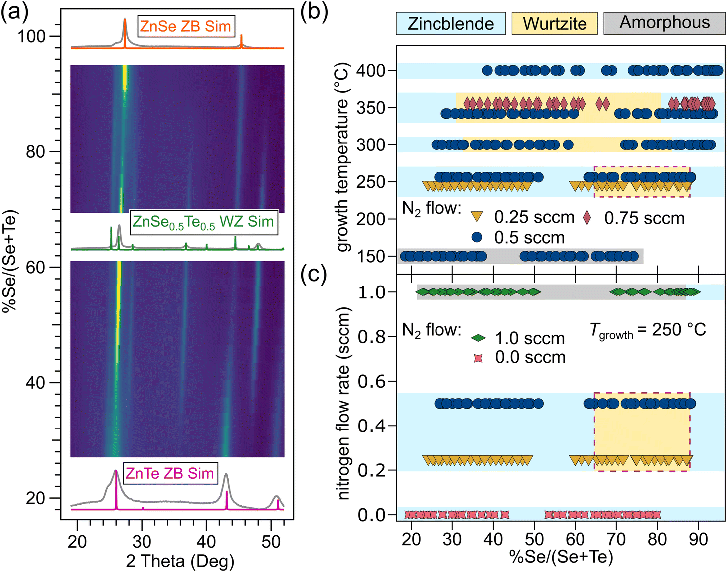 | ||
| Fig. 1 Structural data for N-doped ZnSe1−xTex. (a) Diffraction heat map from a sample library of N-doped ZnSe1−xTex (Tgrowth = 350 °C, QN2 = 0.5 sccm) indicates WZ in alloys. The color scale is the measured intensity in arbitrary units, with yellow indicating a diffraction peak. (b) Growth phase map of N-doped ZnSe1−xTex as a function of temperature. (c) Growth phase map of N-doped ZnSe1−xTex grown at 250 °C as a function of N2 flow rate. In (b) and (c), the WZ phase is indicated when WZ peaks become visible in diffraction patterns, generally implying a mixture of WZ and ZB phases. In panes (b) and (c), the WZ regions highlighted by red dashes at the perimeter are the same samples. | ||
Fig. 1(c) shows a larger number of flow conditions for films grown at 250 °C. At a N2 flow rate of 1.0 sccm, the films became amorphous until nearly pure ZnSe alloy compositions, where a ZB signal was observed. Films grown without the N2 dopant did not exhibit any indication that a WZ phase was present at any alloy composition. In a similar fashion to reducing temperature, reducing the N2 flow rate tends to make samples more Te-rich for a given set of growth conditions.
Cross-sectional scanning electron micrographs collected from undoped (ZB) and N-doped (WZ) ZnSe0.5Te0.5 are shown in Fig. 2. Images are provided in both low magnification (Fig. 2(a) and (b)) and high magnification (Fig. 2(c) and (d)). Clear microstructural changes are observed between the undoped (panes 2(a) and 2(c)) and doped (panes 2(b) and 2(d)) samples. In particular, the undoped film appears denser, especially close to the film surface. Dark regions from the undoped film appear sharp and columnar, likely due to entire crystallites shearing off during mechanical cleaving to prepare the imaged surface. On the other hand, the N-doped film exhibits larger rounded voids, which seem unlikely to have formed during cleaving. We hypothesize that these voids were instead formed from N2 trapped during the growth process. Gaseous N2 escaping could then be responsible for the rougher surface observed from the N-doped film.
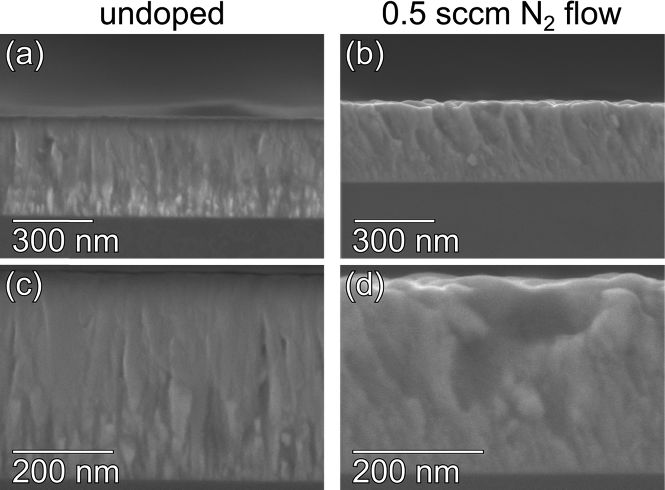 | ||
| Fig. 2 Cross-sectional scanning electron micrographs from ZnSe0.5Te0.5 thin films. Panes (a) and (c) are undoped whereas panes (b) and (d) are doped by 0.5 sccm N2 flow during growth. The doped film exhibits larger, rounded voids, especially near its (rougher) surface. | ||
To better characterize the WZ alloys, a N-doped ZnSe0.5Te0.5 sample grown at 350 °C was selected for high-resolution grazing incidence wide angle X-ray scattering (GIWAXS) measurements. Fig. 3(a) shows diffraction from the film alongside simulated ZnSe0.5Te0.5 WZ and ZB powder diffraction patterns with lattice parameters adjusted to fit the experimental data (a = 4.072 Å and c = 6.716 Å for WZ). A schematic of this WZ structure is shown in the inset to Fig. 3(a). The experimental data match the peak positions of the simulated WZ pattern, and even on a logarithmic scale all of the experimentally observed diffraction features can be attributed to WZ. While many of the ZB and WZ diffraction peaks overlap, the lack of any additional signals unique to ZB ZnSe0.5Te0.5 (cf.Fig. 3(a), green trace), highlights that the N-induced phase transition can be used to prepare phase pure WZ ZnSe0.5Te0.5 alloys, which was not previously achieved in N-doped WZ ZnSe grown by pulsed laser deposition (PLD).4 Deviations between the relative peak intensities between experimental data and simulated WZ are likely from preferential orientation (texture) of crystallites in the sputtered thin films.
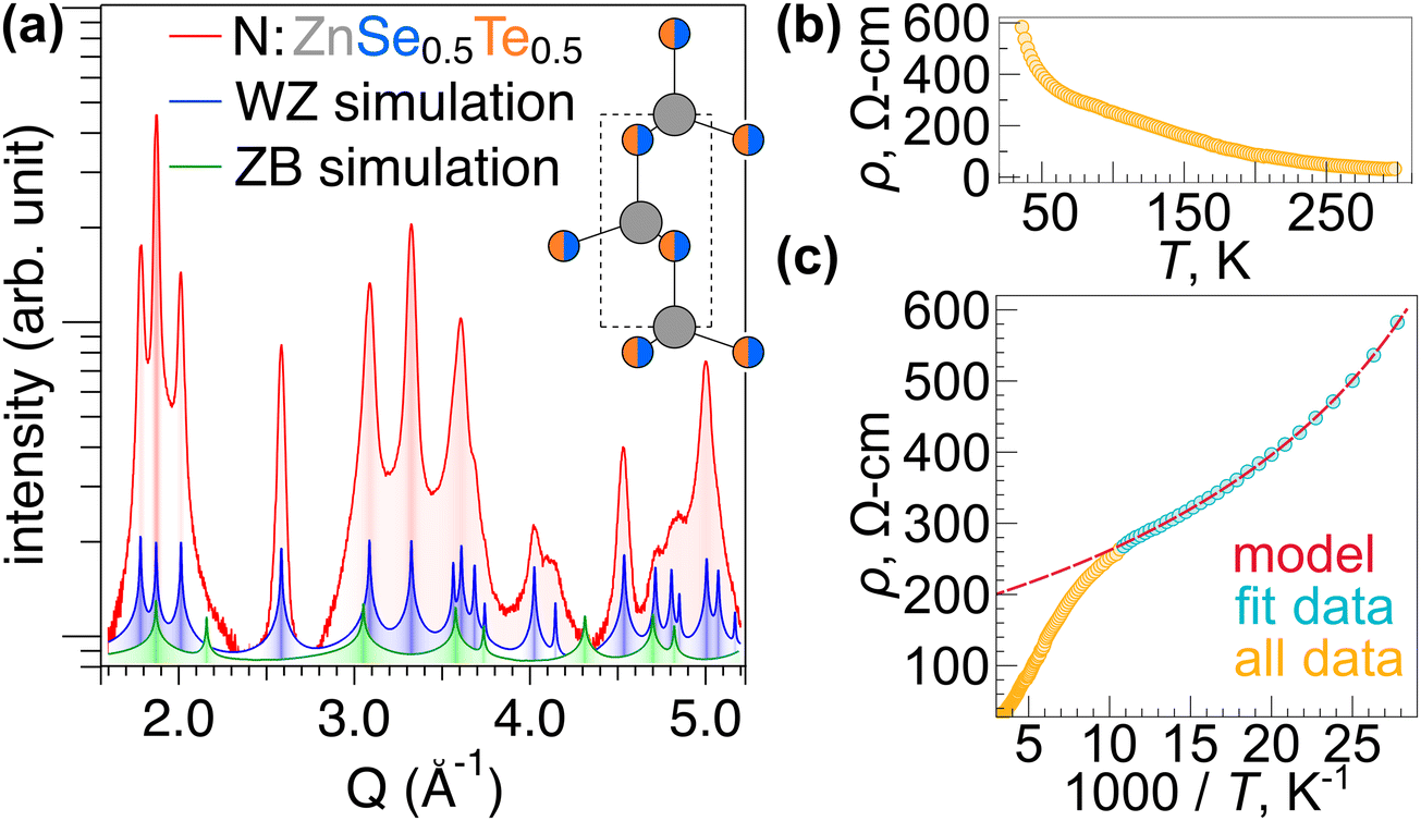 | ||
| Fig. 3 Characterization of N-doped WZ ZnSe0.5Te0.5. (a) Synchrotron XRD from a N-doped ZnSe0.5Te0.5 thin film. The experimental fingerprint matches the simulated wurtzite pattern without any additional features. (b) Temperature-dependent resistivity. (c) Resistivity plotted as a function of inverse T with a combined Arrhenius + variable range hopping model fit to data below 100 K. | ||
A phase-pure WZ ZnSe0.5Te0.5 sample grown on an insulating substrate was also subjected to variable temperature electronic transport measurements, collected in van der Pauw geometry. Fig. 3(b) shows that resistivity increases as temperature decreases, as expected from a semiconducting material. However, the data cannot be fit to a simple activation model. At low temperatures, disordered semiconductors will often exhibit transport deviating from a simple activation-across-a-gap (Arrhenius) model. The data are better described by models such as Mott variable range hopping (VRH) wherein localized defect states—rather than bands—mediate the transport.31 For 3D VRH, the conductivity-temperature dependence takes the form 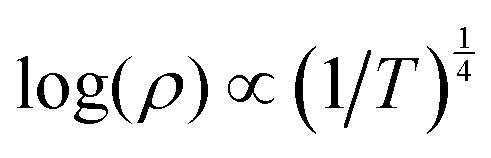 . Following prior work,32–34 we employ a mixed transport model combining Arrhenius and 3D VRH mechanisms of the form
  . Fig. 3(c) plots the same resistivity data as a function of inverse temperature. There is a clear change in behavior at ca. 100 K, so we apply the model between 35–100 K, indicated in the plot by blue circles. The combined model fits the data well in this range (R2 = 0.999993), and while it suggests a combination of band- and defect-mediated transport mechanisms, the VRH effect appears dominant (fit coefficients B/A = 45). Above 100 K, there is an inflection point in the data and the fit rapidly diverges, suggesting a change in transport physics, likely due to thermal activation into the intrinsic transport bands vs. the defect states governing VRH. Undoped ZnSe0.5Te0.5 films made in this study were too resistive to perform transport measurements on, thus confirming that the nitrogen acts as a dopant in addition to inducing a structural change to WZ.
To determine the carrier type, we performed ambient-temperature Hall effect measurements on a N-doped ZnSe0.5Te0.5 sample. We measured a p-type carrier density of p = 1 × 1019 cm−3 and a carrier mobility of μ = 0.05 cm2 V−1 s−1. Such carrier densities are observed in N-doped ZB ZnTe but are higher than in ZnSe and suggest less than unity dopant activation given the percent scale concentration of N measured by AES. The low mobility is near the threshold that can be measured using DC Hall techniques, so we performed multiple measurements under different conditions to ensure a consistent result. Such p-type transport is expected from N substitution onto chalcogen sites and corroborated by the positive sign of the Seebeck coefficient. Pristine ZB ZnSe and ZnTe semiconductors have high hole mobility (up to 1000 cm2 V−1 s−1 at cryogenic temperatures)35 as do p-type WZ semiconductors such as GaN (>150 cm2 V−1 s−1 at 150 K),36 so it is likely that WZ ZnSe0.5Te0.5 would also have an intrinsic low-temperature charge carrier mobility on order of 100 cm2 V−1 s−1 or greater. Thus, we attribute the low mobility here to defects or voids (cf.Fig. 2), which the VRH character of the resistivity suggests may persist at nanoscopic length scales. More pristine WZ ZnSe0.5Te0.5 should be pursued to better understand the carrier transport.
In an effort to better understand the nanostructure of the N-doped film where VRH behavior is observed, we prepared a lamella from a nitrogen doped ZnSe0.5Te0.5 thin film to collect transmission electron microscopy (TEM) data. Data from this study are shown in Fig. 4. Fig. 4(a) was collected in bright field mode and shows a polycrystalline sample. Highlighted by gold circles are several small (ca. 10 nm) bright spots. Such spots could arise from less scattering of the electron beam through the thickness of the lamella, as would be expected by voids filled with N2 or vacuum where N2 gas previously resided, in qualitative agreement with the SEM data in Fig. 2. Similar features have been observed in N2 nano-inclusions in diamond.37 The energy dispersive X-ray spectroscopy map in Fig. 4(b) shows uniform distribution of all elements. A lack of signal from discrete N2-filled voids is at first surprising. However, the number density of an ideal gas at ambient conditions is on the order of 1019 cm−3, so it is likely impossible to see trapped N2 gas over the background signal of N in the lattice, which is at minimum of similar magnitude as determined by the carrier density, and up to ca. 1021 cm−3 based on a 5% incorporation level in ZnSe0.5Te0.5, the upper limit we determined from AES. Fig. 4(c) shows a high-magnification micrograph highlighting two void-like features that are only a few nm across; in these features, which are much smaller than most of the crystalline grains, crystalline lattice planes are either disrupted or not observed. These features are further highlighted to the right of the main pane. While we cannot preclude the possibility that they were introduced during preparation of the lamella since similar features are often associated with focused ion beam damage, they are of a nanoscopic size scale that could play a role in hole transport and inducing VRH behavior. If they did occur during growth, their irregular—as opposed to faceted—morphology likely arises from the kinetically controlled nature of sputter processing.
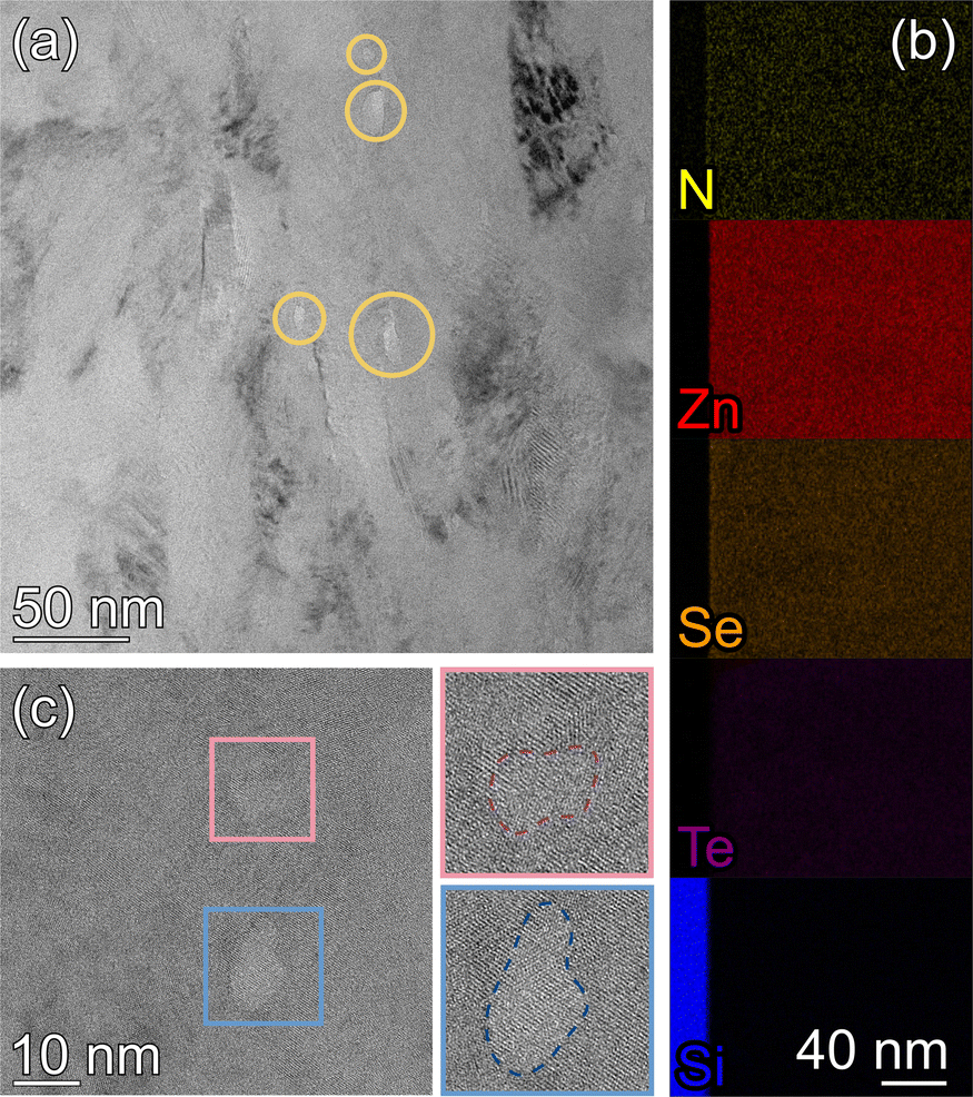 | ||
| Fig. 4 Transmission electron microscopy (TEM) data collected from N-doped ZnSe0.5Te0.5. (a) Lighter contrast spots in bright field mode suggest less scattering from regions containing N2 pockets. (b) Energy dispersive X-ray spectroscopy (EDS) maps show uniform distributions of all elements. (c) Few-nm void-like features are observed in high-magnification imaging. | ||
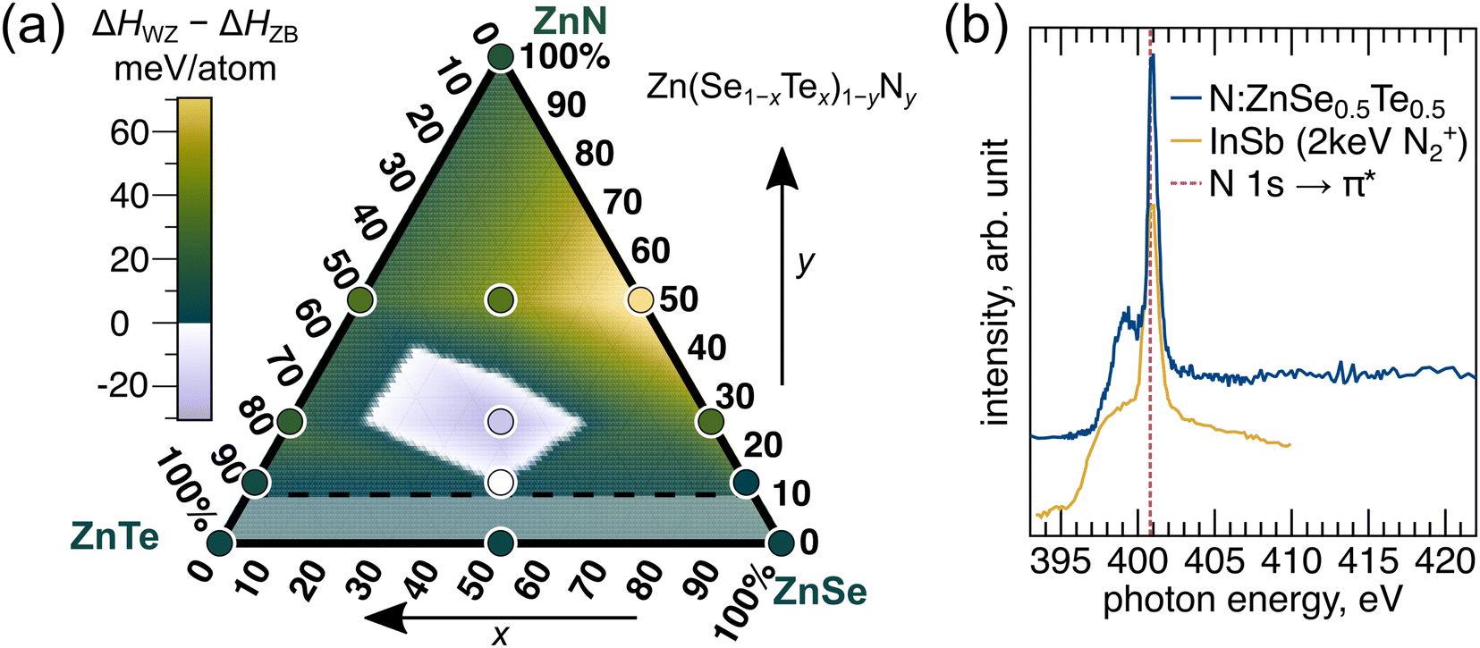
To assess whether WZ stabilization is due to enthalpic degrees of freedom, we performed survey density functional theory (DFT) calculations within the zero temperature (0 K) approximation to compare WZ and ZB polymorph energies in the pseudo-quaternary Zn(Se1−xTex)1−yNy (x = 0, 0.5, 1 and y = 0, 0.125, 0.25, 0.5, 1) subspace. Computational results from 269 unique structures across the phase space are summarized in Table 1 and Fig. 5(a) as a ternary phase diagram, highlighting the formation enthalpy difference between the lowest energy bulk WZ and ZB crystalline phases. Rather than computationally more expensive approaches requiring structure sampling and large supercells, this simple approach was chosen to generate a cursory theoretical understanding of phase stability when nitrogen is introduced into the system. We note that an inherent limitation of this approach is that a charge unbalanced system may result from replacing chalcogen ions (Se2−, Te2−) in ZnSe1−xTex with N3− ions while constraining to stoichiometric ZB or WZ crystal structures.
| Compound | ΔHWZ − ΔHZB (meV per atom) |
|---|---|
| ZnSe | +4.8 |
| ZnTe | +5.2 |
| ZnSe0.5Te0.5 | +4.8 |
| ZnSe0.875N0.125 | +0.3 |
| ZnTe0.875N0.125 | +8.0 |
| ZnSe0.4375Te0.4375N0.125 | −0.1 |
| ZnSe0.75N0.25 | +27.3 |
| ZnTe0.75N0.25 | +19.7 |
| ZnSe0.375Te0.375N0.25 | −17.9 |
| ZnSe0.5N0.5 | +67.8 |
| ZnTe0.5N0.5 | +29.9 |
| ZnSe0.25Te0.25N0.5 | +31.9 |
| ZnN | +14.1 |
 | ||
| Fig. 5 (a) Wurtzite (WZ) polymorph energy referenced against zinc blende (ZB) for various Zn(Se1−xTex)1−yNy compositions, computed by DFT. The WZ polymorph is comparable or more favorable than ZB at low nitrogen concentrations and intermediate x. The experimental range of nitrogen concentrations (<5%) are shown as a shaded region below the horizontal dashed line. (b) N K-edge XANES data collected from N-doped ZnSe0.5Te0.5. The strong signal at 400.8 eV has been attributed to interstitial N2 in both nitride and N-doped compound semiconductors. For example, InSb implanted with N2 (yellow trace adapted from ref. 38) is shown as a comparison. | ||
The results of our calculations are detailed in Table 1 and Fig. 5(a). The color scale in Fig. 5(a) is designed such that compositions that favor WZ (negative ΔHWZ − ΔHZB) are in the purple-white range with darker color indicating a larger polymorph energy difference, whereas compositions that favor ZB (positive ΔHWZ − HZB) are in the green-yellow range with lighter color indicating a larger polymorph energy difference. Also shown is a shaded region below nitrogen concentrations of 5% (or 10% on the ZnN-axis of Fig. 5(a)), corresponding to the upper-limit of total nitrogen concentration measured by AES. In most cases we find ZB to be the more stable polymorph, but the energy difference is generally low, with ZnSe0.5N0.5 being the only compound where we calculate a magnitude of ΔHWZ − ΔHZB greater than 32 meV per atom.
Interestingly, the WZ polymorph is stabilized over ZB at compositions with low nitrogen concentration and x = 0.5. Therefore, these results qualitatively support our experimental findings: there is a region of phase space at low N concentrations and around x = 0.5 in which the WZ phase is predicted to stabilize. A linear interpolation on the surveyed points highlights the region where our calculations suggest WZ is the most stable polymorph. For the ternary alloy ZnSe0.5Te0.5 with no nitrogen, we find that ZB is again the most stable polymorph, but by <5 meV per atom. Our computational survey does not include dopant levels of N, which would require very large supercells, so the white-purple WZ region in the interpolation may extend lower than shown. A dedicated computational effort focusing on defect formation energies of this system should be performed to develop a better thermochemical understanding of WZ phase stability.
Bulk thermodynamics aside, the difference in surface energy between ZB and WZ could potentially provide an additional stabilization mechanism for N-doped WZ ZnSe1−xTex. Lower WZ surface energies compared to ZB are well known to stabilize WZ in nanostructured semiconductor systems, even when bulk analogues form in the ZB crystal structure.39–42 This could help explain why ZB is observed across the entire N-doped ZnSe1−xTex alloy space in films grown by molecular beam epitaxy,24 which are usually smooth and dense, but not in films grown here by sputtering or grown previously by PLD.4 Ablated plumes have significantly more kinetic energy than thermally evaporated species and are more likely to create interstitials, voids, and other defects.43 Such features in sputtered and PLD films increase the effective surface area of crystallites, and thus the contribution from the surface energy. Taking this idea a step further, WZ stability would further increase in doped films if N2 gas trapped in the films during growth increased the microstructural feature density. This is consistent with the microscopy data found in Fig. 2 and 4, which indicate that voids were present in the N-doped samples but not in the undoped samples, as well as the VRH transport character found in doped films.
While the uniformity of the EDS maps in Fig. 4(b) does not suggest there were regions with excess N2, this gas is likely invisible over the background N in the ZnSe0.5Te0.5 lattice. To check if N2 was indeed trapped in N-doped ZnSe1−xTex, we collected X-ray absorption near edge spectra (XANES) at the N K-edge from the same N-doped ZnSe0.5Te0.5 thin film shown in Fig. 3(a), presented here in Fig. 5(b). We observe a strong signal at 400.8 eV that is associated with the N 1s → π* transition in molecular N2 and known to be present when interstitial N2 is trapped in compound semiconductors.38,44,45Fig. 5(b) also shows a reference example of InSb implanted with 2 keV N2+, adapted from Petravic et al.38 Thus, we conclude that molecular N2 is very likely to be present at voids and/or grain boundaries of the N-doped ZnSe0.5Te0.5 film. Though the voids evident in Fig. 2 only contact a small fraction of crystalline surface area, it is likely that these first formed as N2 gas trapped as nanoscopic inclusions, the largest of which are observed by TEM in Fig. 4, by continuous introduction of molecular N2 into the films, and eventually conglomerated near the surface (Fig. 2). We propose such a mechanism helps stabilize WZ through surface energy effects, complementing any bulk enthalpic stabilization. Because transport data (Fig. 3) could only be collected from films containing nitrogen, we also conclude that some small fraction of N is also doped onto chalcogen sites.
In conclusion, we have grown a series of nitrogen doped ZnSe1−xTex thin films by RF sputtering and have found that intermediate compositions form in the wurtzite structure, as opposed to the well-known, previously reported zinc blende structure. The wurtzite phase is observed over a range of compositions and growth temperatures. Temperature-dependent electronic transport measurements collected from 35–300 K suggest that the properties of phase-pure wurtzite N-doped ZnSe0.5Te0.5 prepared during this study are still governed by defect-mediated rather than intrinsic transport. The stabilization of wurtzite over zinc blende in nitrogen doped alloys is attributed to a combination of more favorable wurtzite polymorph energies from dilute nitrogen concentrations and trapping N2 during growth, which leads to a stronger energetic contribution from the surface energy. Future research on N-doped ZnSe1−xTex alloys should consider wurtzite polymorphism, and attempts to prepare high-density, phase-pure wurtzite with intrinsic electronic transport would be particularly valuable.
Methods
Growth
ZnSe1−xTex was grown via RF sputtering from compound targets on silicon substrates with either native or 100 nm SiO2 layers. Before deposition, the chamber was pumped to a maximum base pressure of 5 × 10⁻⁷ torr. ZnSe and ZnTe targets were obliquely positioned on opposite ends of a horizontal axis relative to the substrates to generate a linear anionic compositional gradient across the 2′′ substrates. Substrates were clamped to platens heated by a serpentine SiC resistance coil and rested at their temperature setpoint for a minimum of one hour before deposition began. Sputtering was performed under a flow of 16 sccm of Ar at a pressure of 2.7 mTorr. The N dopant was introduced into films by gaseous N2 flow at the substrate, moderated by a mass flow controller. Following a period of pre-sputtering, the combinatorial alloy films were deposited for 90 minutes. Film thicknesses were measured by X-ray fluorescence and confirmed by stylus profilometry. 90 minute growth times resulted in films with thicknesses ranging from 150–400 nm. N2 flows and temperature setpoints were varied between growths. Sputtering gun powers were chosen to create a compositional gradient that spanned the majority of the ZnSe1−xTex alloy space.Experimental characterization
Laboratory X-ray diffraction experiments were carried out using Cu Kα radiation on a Bruker D8 Discover diffractometer equipped with a two-dimensional detector. Detector images were integrated in the χ dimension to create intensity vs. 2θ profiles. Relative Zn, Se, and Te compositions were determined using ambient atmosphere X-ray fluorescence measurements with a typical accuracy of ca. ±2% and unless otherwise noted, the anion/cation ratio was 0.5 within this window. We thus report composition using the chalcogen anions. During calibration, samples grown with N2 flow were characterized for depth-dependent composition by Auger Electron Spectroscopy. Interfering signals made quantification difficult, but we were able to conclude N concentrations were <5%. Samples were prepared for cross-sectional SEM immediately before analysis by mechanical cleaving. This exposed fresh cross-sections of the films perpendicular to the growth plane. SEM micrographs were acquired on a Hitachi S-4800 SEM operating at 5 kV in secondary electron imaging mode. The lamella for TEM analysis was prepared using conventional lift out techniques on an FEI dual beam FIB/SEM after capping with a carbon based epoxy. TEM imaging was performed on an FEI Technai Osiris microscope operated at 200 kV in bright field and high-resolution modes. EDS spectra were acquired using a Bruker Quantax.High resolution synchrotron grazing incidence wide angle X-ray scattering (GIWAXS) measurements were performed on select samples at beamline 11-3 at the Stanford Synchrotron Radiation Lightsource (SSRL), SLAC National Accelerator Laboratory. The data were collected with a Rayonix 225 area detector at room temperature using a wavelength of λ = 0.9744 Å, 3° incident angle, a 150 mm sample-to-detector distance, and a spot size of 50 μm × 150 μm. The detector image was integrated and peaks in the resulting intensity vs. 2θ profile were fit by the LeBail method as implemented in GSAS-II.46
High-resolution N K-edge X-ray absorption near-edge spectroscopy (XANES) measurements were carried out on thin films at room temperature at SSRL beamline 10-1. Measurements were carried out under high vacuum conditions of ∼2.7 × 10⁻⁶ Pa (∼2 × 10⁻⁸ torr) with a ring current of 500 mA. The synchrotron radiation was monochromatized using the beamline's 1000 line per mm monochromator with entrance and exit slits of 27 μm. A transition edge sensor (TES) spectrometer47 was used to collect resonant inelastic X-ray scattering (RIXS) planes with a resolution of 2 eV. The energy measured by the TES was calibrated by periodically measuring a reference sample of graphite, BN, Fe2O3, NiO, CuO, and ZnO, which provide a stable set of emission lines. With the TES, we employed an energy region of interest to select the N K-edge emission to create partial-fluorescence-yield XAS.
Combinatorial data were analyzed using the COMBIgor48 analysis package and processed through the NREL high-throughput research data infrastructure.49 Data discussed in this work will be made publicly available in the NREL high-throughput experimental materials database (HTEM).50
Calculations
Density functional theory (DFT) calculations were performed with the Vienna Ab Initio Simulation Package (VASP)51,52 using the projector augmented wave (PAW) method.53,54 The Perdew–Burke–Ernzerhof (PBE) Generalized Gradient Approximation (GGA)55 formulation of the exchange–correlation functional is used, with the cutoff, convergence, and correction criteria as described by the Materials Project formalism.56,57 Ordered polymorph structures of wurtzite, zinc blende, and rocksalt were generated for Zn(Se1−xTex)1−yNy (x = 0, 0.5, 1 and y = 0, 0.125, 0.25, 0.5, 1). The enumlib package was used to enumerate all possible unique orderings for the smallest unit cell size for each polymorph and composition (up to 12 orderings per WZ and ZB polymorph), amounting to 269 total structures, and the pymatgen structure matching routine was used to very structure type after each DFT relaxation.Conflicts of interest
There are no conflicts to declare.Acknowledgements
This work was performed in part at National Renewable Energy Laboratory, operated by Alliance for Sustainable Energy, LLC, for the U.S. Department of Energy (DOE) under Contract no. DE-AC36-08GO28308. This material is based upon work performed by the Liquid Sunlight Alliance, a DOE Energy Innovation Hub, supported by the U.S. DOE, Office of Science, Office of Basic Energy Sciences, under Award Number DE-SC0021266. T. C. acknowledges support from DOE Office of Science, Office of Workforce Development for Teachers and Scientists under the Science Undergraduate Laboratory Internship program. R. W. S. was supported by the Director's Fellowship within NREL's Laboratory Directed Research and Development program. Use of the Stanford Synchrotron Radiation Lightsource, SLAC National Accelerator Laboratory, is supported by the U.S. DOE, Office of Science, Office of Basic Energy Sciences under Contract No. DE-AC02-76SF00515. Computational work was supported by the U.S. DOE, Office of Science, Office of Basic Energy Sciences, Materials Sciences and Engineering Division under Contract No. DE-AC02-05-CH11231 (Materials Project program KC23MP). The authors thank Dr Craig Perkins for assistance with AES measurements and data interpretation, Dr Sang-Jun Lee for assistance with the XANES measurements, and Dr Charles J. Titus for assistance with XANES data processing, and Eurofins EAG for performing lamella prep and TEM measurements. The views expressed in this article do not necessarily represent the views of the DOE or the U.S. Government.References
- C.-Y. Yeh, Z. W. Lu, S. Froyen and A. Zunger, Zinc blende-wurtzite polytypism in semiconductors, Phys. Rev. B: Condens. Matter Mater. Phys, 1992, 46, 10086 CrossRef.
- A. Jain, S. P. Ong, G. Hautier, W. Chen, W. D. Richards, S. Dacek, S. Cholia, D. Gunter, D. Skinner, G. Ceder and K. A. Persson, Commentary: The materials project: A materials genome approach to accelerating materials innovation, APL Mater., 2013, 1, 011002 CrossRef.
- Z. Z. Bandić and Z. Ikonić, Electronic structure of (Zn,Cd)(S,Se)-based polytype superlattices, Phys. Rev. B: Condens. Matter Mater. Phys., 1995, 51, 9806 CrossRef PubMed.
- X. Zhang, D. Wang, M. Beres, L. Liu, Z. Ma, P. Y. Yu and S. S. Mao, Zinc blende-wurtzite phase transformation of ZnSe films by pulsed laser deposition with nitrogen doping, Appl. Phys. Lett., 2013, 103, 082111 CrossRef.
- C. Wilhelm, A. Larrue, X. Dai, D. Migas and C. Soci, Anisotropic photonic properties of III–V nanowires in the zinc blende and wurtzite phase, Nanoscale, 2012, 4, 1446–1454 RSC.
- S. Park, C. W. Lee, M. G. Kang, S. Kim, H. J. Kim, J. E. Kwon, S. Y. Park, C. Y. Kang, K. S. Hong and K. T. Nam, A ferroelectric photocatalyst for enhancing hydrogen evolution: Polarized particulate suspension, Phys. Chem. Chem. Phys., 2014, 16, 10408–10413 RSC.
- Y. L. Huang, W. S. Chang, C. van Nguyen, H. J. Liu, K. A. Tsai, J. W. Chen, H. H. Kuo, W. Y. Tzeng, Y. C. Chen, C. L. Wu, C. W. Luo, Y. J. Hsu and Y. H. Chu, Tunable photoelectrochemical performance of Au/BiFeO3 heterostructure, Nanoscale, 2016, 8, 15795–15801 RSC.
- S. Li, J. Zhang, B. P. Zhang, W. Huang, C. Harnagea, R. Nechache, L. Zhu, S. Zhang, Y. H. Lin, L. Ni, Y. H. Sang, H. Liu and F. Rosei, Manipulation of charge transfer in vertically aligned epitaxial ferroelectric KNbO3 nanowire array photoelectrodes, Nano Energy, 2017, 35, 92–100 CrossRef CAS.
- T. Tao, T. Zhi, B. Liu, M. Li, Z. Zhuang, J. Dai, Y. Li, F. Jiang, W. Luo, Z. Xie, D. Chen, P. Chen, Z. Li, Z. Zou, R. Zhang and Y. Zheng, Significant improvements in InGaN/GaN nano-photoelectrodes for hydrogen generation by structure and polarization optimization, Sci. Rep., 2016, 6(1), 1–8 CrossRef.
- J. Johnson, N. Bakranov, M. Moniruddin, R. Iskakov, S. Kudaibergenov and N. Nuraje, Spontaneous polarization field-enhanced charge separation for an iron oxide photo-catalyst, New J. Chem., 2017, 41, 15528–15532 RSC.
- D. Spirkoska, J. Arbiol, A. Gustafsson, S. Conesa-Boj, F. Glas, I. Zardo, M. Heigoldt, M. H. Gass, A. L. Bleloch, S. Estrade, M. Kaniber, J. Rossler, F. Peiro, J. R. Morante, G. Abstreiter, L. Samuelson and A. Fontcuberta I Morral, Structural and optical properties of high quality zinc blende/wurtzite GaAs nanowire heterostructures, Phys. Rev. B: Condens. Matter Mater. Phys., 2009, 80, 245325 CrossRef.
- M. Heiss, S. Conesa-Boj, J. Ren, H. H. Tseng, A. Gali, A. Rudolph, E. Uccelli, F. Peiró, J. R. Morante, D. Schuh, E. Reiger, E. Kaxiras, J. Arbiol and A. Fontcuberta I Morral, Direct correlation of crystal structure and optical properties in wurtzite/zinc blende GaAs nanowire heterostructures, Phys. Rev. B: Condens. Matter Mater. Phys., 2011, 83, 045303 CrossRef.
- H. Y. Xu, Z. Liu, Y. Liang, Y. Y. Rao, X. T. Zhang and S. K. Hark, Structure and photoluminescence of wurtzite/zinc blende heterostructure GaN nanorods, Appl. Phys. Lett., 2009, 95, 133108 CrossRef.
- J. R. Chelikowsky and M. L. Cohen, Nonlocal pseudopotential calculations for the electronic structure of eleven diamond and zinc blende semiconductors, Phys. Rev. B: Condens. Matter Mater. Phys., 1976, 14, 556 CrossRef CAS.
- R. Woods-Robinson, Y. Han, H. Zhang, T. Ablekim, I. Khan, K. A. Persson and A. Zakutayev, Wide band gap chalcogenide semiconductors, Chem. Rev., 2020, 120, 4007–4055 CrossRef CAS PubMed.
- V. Ryzhikov, N. Starzhinskiy, L. Gal’Chinetskii, P. Gáshin, D. Kozin and E. Danshin, New semiconductor scintillators ZnSe(Te, O) and integrated radiation detectors based thereon, IEEE Trans. Nucl. Sci., 2001, 48, 356–359 CAS.
- A. Luque and A. Martí, The intermediate band solar cell: Progress toward the realization of an attractive concept, Adv. Mater., 2010, 22, 160–174 CrossRef PubMed.
- O. Andriuc, M. Siron, J. H. Montoya, M. Horton and K. A. Persson, Automated adsorption workflow for semiconductor surfaces and the application to zinc telluride, J. Chem. Inf. Model., 2021, 61, 3908–3916 CrossRef.
- X. Xiong, M. Forster, J. D. Major, Y. Xu and A. J. Cowan, Time-resolved spectroscopy of ZnTe photocathodes for solar fuel production, J. Phys. Chem. C, 2017, 121, 22073–22080 CrossRef.
- R. Hellwarth and P. Christensen, Nonlinear optical microscopic examination of structure in polycrystalline ZnSe, Opt. Commun., 1974, 12, 318–322 CrossRef.
- T. D. Krauss and F. W. Wise, Femtosecond measurement of nonlinear absorption and refraction in CdS, ZnSe, and ZnS, Appl. Phys. Lett., 1998, 65, 1739 CrossRef.
- I. W. Tao, M. Jurkovic and W. I. Wang, Doping of ZnTe by molecular beam epitaxy, Appl. Phys. Lett., 1998, 64, 1848 CrossRef.
- Y. Fan, J. Han, R. L. Gunshor, J. Walker, N. M. Johnson and A. V. Nurmikko, The study of nitrogen doping in ZnSe and ZnSe:Te, J. Electron. Mater., 1995, 24(3), 131–135 CrossRef.
- W. Lin, B. X. Yang, S. P. Quo, A. Elmoumni, F. Fernandez and M. C. Tamargo, Molecular-beam epitaxy growth and nitrogen doping of ZnSe1−xTex alloys grown on InP substrates, Appl. Phys. Lett., 1999, 75, 2608 CrossRef CAS.
- A. Ohtake, J. Nakamura, M. Terauchi, F. Sato, M. Tanaka, K. Kimura and T. Yao, Wurtzite–zinc blende polytypism in ZnSe on GaAs(111)A, Phys. Rev. B: Condens. Matter Mater. Phys., 2001, 63, 195325 CrossRef.
- S. Siol, A. Holder, J. Steffes, L. T. Schelhas, K. H. Stone, L. Garten, J. D. Perkins, P. A. Parilla, M. F. Toney, B. D. Huey, W. Tumas, S. Lany and A. Zakutayev, Negative-pressure polymorphs made by heterostructural alloying, Sci Adv., 2018, 4(4), eaaq1442 CrossRef.
- Y. Han, A. M. Holder, S. Siol, S. Lany, Q. Zhang and A. Zakutayev, Zinc-stabilized manganese telluride with wurtzite crystal structure, J. Phys. Chem. C, 2018, 122, 18769–18775 CrossRef CAS.
- R. Woods-Robinson, Y. Han, J. S. Mangum, C. L. Melamed, B. P. Gorman, A. Mehta, K. A. Persson and A. Zakutayev, Combinatorial tuning of structural and optoelectronic properties in CuxZn1−xS, Matter, 2019, 1, 862–880 CrossRef.
- Y. Han, S. L. Millican, J. Liu, S. R. Bauers, S. Siol, S. Lany, M. Al-Jassim, C. B. Musgrave, A. M. Holder and A. Zakutayev, Wurtzite materials in alloys of rock salt compounds, J. Mater. Res., 2020, 35, 972–980 CrossRef CAS.
- Y. Fan, J. Han and L. He, Observations on the limits to P-type doping in ZnSe, Appl. Phys. Lett., 1994, 65, 1001 CrossRef.
- N. F. Mott, Metal-insulator transition, Rev. Mod. Phys., 1968, 40, 677 CrossRef.
- G. Catalan, R. M. Bowman and J. M. Gregg, Metal-insulator transitions in NdNiO3 thin films, Phys. Rev. B: Condens. Matter Mater. Phys., 2000, 62, 7892 CrossRef.
- Q. Jin, J. Zhao, M. A. Roldan, W. Qi, S. Lin, S. Chen, H. Hong, Y. Fan, D. Rong, H. Guo, C. Ge, C. Wang, J.-O. Wang, S. Wang, K. Jin and E.-J. Guo, Anisotropic electronic phase transition in CrN epitaxial thin films, Appl. Phys. Lett., 2022, 120, 073103 CrossRef.
- Y. Y. Zhu, R. J. Wang, W. Li, L. Yong, X. Rui, S. Jing, L. H. An, D. H. Sun, L. Wang, Y. Liu, R. Xiong and J. Shi, Transport behavior in spinel oxide MgTi2O4, Chin. Phys. Lett., 2014, 31, 097201 CrossRef.
- M. Aven and B. Segall, Carrier mobility and shallow impurity states in ZnSe and ZnTe, Phys. Rev., 1963, 130, 81 CrossRef.
- S. Poncé, D. Jena and F. Giustino, Route to high hole mobility in GaN via reversal of crystal-field splitting, Phys. Rev. Lett., 2019, 123, 096602 CrossRef.
- J. Rudloff-Grund, F. E. Brenker, K. Marquardt, F. V. Kaminsky and A. Schreiber, STEM EDX nitrogen mapping of nanoinclusions in milky diamonds from juina, brazil, using a windowless silicon drift detector system, Anal. Chem., 2016, 88, 5804–5808 CrossRef PubMed.
- M. Petravic, Q. Gao, D. Llewellyn, P. N. K. Deenapanray, D. Macdonald and C. Crotti, Broadening of vibrational levels in X-ray absorption spectroscopy of molecular nitrogen in compound semiconductors, Chem. Phys. Lett., 2006, 425, 262–266 CrossRef.
- F. Glas, J. C. Harmand and G. Patriarche, Why does wurtzite form in nanowires of III-V zinc blende semiconductors?, Phys. Rev. Lett., 2007, 99, 146101 CrossRef.
- L. Manna, D. J. Milliron, A. Meisel, E. C. Scher and A. A. P. Alivisatos, Controlled growth of tetrapod-branched inorganic nanocrystals, Nat. Mater., 2003, 2, 382 CrossRef.
- F. Wang and W. E. Buhro, An easy shortcut synthesis of size-controlled bismuth nanoparticles and their use in the SLS growth of high-quality colloidal cadmium selenide quantum wires, Small, 2010, 6, 573–581 CrossRef PubMed.
- A. Myalitsin, C. Strelow, Z. Wang, Z. Li, T. Kipp and A. Mews, Diameter scaling of the optical band gap in individual CdSe nanowires, ACS Nano, 2011, 5, 7920–7927 CrossRef PubMed.
- D. M. Mattox, Handbook of Physical Vapor Deposition (PVD) Processing, Elsevier Inc., 2010 Search PubMed.
- J. D. Hecht, F. Frost, D. Hirsch, H. Neumann, A. Schindler, A. B. Preobrajenski and T. Chassé, Interstitial nitrogen induced by low-energy ion beam nitridation of AIII–BV semiconductor surfaces, J. Appl. Phys., 2001, 90, 6066 CrossRef.
- B. J. Ruck, A. Koo, U. D. Lanke, F. Budde, S. Granville, H. J. Trodahl, A. Bittar, J. B. Metson, V. J. Kennedy and A. Markwitz, Quantitative study of molecular N2 trapped in disordered GaN:O films, Phys. Rev. B: Condens. Matter Mater. Phys., 2004, 70, 235202 CrossRef.
- B. H. Toby and R. B. von Dreele, GSAS-II: The genesis of a modern open-source all purpose crystallography software package, J. Appl. Crystallogr., 2013, 46, 544–549 CrossRef.
- S. J. Lee, C. J. Titus, R. Alonso Mori, M. L. Baker, D. A. Bennett, H. M. Cho, W. B. Doriese, J. W. Fowler, K. J. Gaffney, A. Gallo, J. D. Gard, G. C. Hilton, H. Jang, Y. il Joe, C. J. Kenney, J. Knight, T. Kroll, J. S. Lee, D. Li, D. Lu, R. Marks, M. P. Minitti, K. M. Morgan, H. Ogasawara, G. C. O’Neil, C. D. Reintsema, D. R. Schmidt, D. Sokaras, J. N. Ullom, T. C. Weng, C. Williams, B. A. Young, D. S. Swetz, K. D. Irwin and D. Nordlund, Soft X-ray spectroscopy with transition-edge sensors at stanford synchrotron radiation lightsource beamline 10-1, Rev. Sci. Instrum., 2019, 90, 113101 CrossRef PubMed.
- K. R. Talley, S. R. Bauers, C. L. Melamed, M. C. Papac, K. N. Heinselman, I. Khan, D. M. Roberts, V. Jacobson, A. Mis, G. L. Brennecka, J. D. Perkins and A. Zakutayev, COMBIgor: Data-analysis package for combinatorial materials science, ACS Comb. Sci., 2019, 21, 537–547 CrossRef.
- K. R. Talley, R. White, N. Wunder, M. Eash, M. Schwarting, D. Evenson, J. D. Perkins, W. Tumas, K. Munch, C. Phillips and A. Zakutayev, Research data infrastructure for high-throughput experimental materials science, Patterns, 2021, 2, 100373 CrossRef PubMed.
- A. Zakutayev, N. Wunder, M. Schwarting, J. D. Perkins, R. White, K. Munch, W. Tumas and C. Phillips, An open experimental database for exploring inorganic materials, Sci. Data, 2018, 5, 1–12 CrossRef.
- G. Kresse and J. Furthmüller, Efficient iterative schemes for ab initio total-energy calculations using a plane-wave basis set, Phys. Rev. B: Condens. Matter Mater. Phys., 1996, 54, 11169 CrossRef.
- G. Kresse and J. Hafner, Ab initio molecular dynamics for liquid metals, Phys. Rev. B: Condens. Matter Mater. Phys., 1993, 47, 558 CrossRef.
- P. E. Blöchl, Projector augmented-wave method, Phys. Rev. B: Condens. Matter Mater. Phys., 1994, 50, 17953 CrossRef.
- G. Kresse and D. Joubert, From ultrasoft pseudopotentials to the projector augmented-wave method, Phys. Rev. B: Condens. Matter Mater. Phys., 1999, 59, 1758 CrossRef.
- J. P. Perdew, K. Burke and M. Ernzerhof, Generalized gradient approximation made simple, Phys. Rev. Lett., 1996, 77, 3865 CrossRef PubMed.
- A. Jain, S. P. Ong, G. Hautier, W. Chen, W. D. Richards, S. Dacek, S. Cholia, D. Gunter, D. Skinner and G. Ceder, Commentary: The materials project: A materials genome approach to accelerating materials innovation, APL Mater., 2013, 1, 11002 CrossRef.
- S. P. Ong, W. D. Richards, A. Jain, G. Hautier, M. Kocher, S. Cholia, D. Gunter, V. L. Chevrier, K. A. Persson and G. Ceder, Python materials genomics (pymatgen): A robust, open-source python library for materials analysis, Comput. Mater. Sci., 2013, 68, 314–319 CrossRef.
| This journal is © The Royal Society of Chemistry 2022 |