DOI:
10.1039/D2TC02335K
(Paper)
J. Mater. Chem. C, 2022,
10, 17602-17610
A machine learning study on superlattice electron blocking layer design for AlGaN deep ultraviolet light-emitting diodes using the stacked XGBoost/LightGBM algorithm†
Received
4th June 2022
, Accepted 28th October 2022
First published on 28th October 2022
Abstract
Aluminium gallium nitride (AlGaN)-based deep ultraviolet (DUV) light-emitting diodes (LEDs) suffer from low internal quantum efficiency (IQE) and serious efficiency droop. One reason for this is the electron leakage and poor hole injection related to the band alignment of the heterojunctions, doping, polarization effect, and others. In the past, the AlGaN/AlGaN superlattice (SL) electron blocking layer (EBL) was proposed to optimize the carrier transport and improve the LED performance. However, the SL-EBL design is a trade-off of multiple physics mechanisms, and the LED efficiency deteriorates when the design is improper. We used extreme gradient boosting (XGBoost) and light gradient boosting machine (LightGBM) stacked machine learning (ML) models to predict various high-performance SL-EBLs considering different compositions, thicknesses, and band offset ratios. Based on the ML model, we propose an easier and experimentally achievable low Al-content SL-EBL (1 nm/5 nm Al0.7Ga0.3N/Al0.58Ga0.42N) that can significantly optimize carrier transport. The improvement in IQE and wall-plug efficiency could be as high as about 70% compared with those of the conventional bulk EBL. Moreover, we analyze the prediction data and reveal the influence of the composition and thickness on the IQE improvement. The composition difference should be enlarged at a higher band offset ratio, which may be explained by the electron potential and polarization modulation. The critical thickness of the optimized SL-EBL is investigated to guarantee effective electron blocking without destroying the material quality, doping modulation, and operating voltage. This work provides a systematic study of SL-EBLs and helps promote the development and application of SL-EBLs for high-efficiency DUV LEDs.
Introduction
Aluminium gallium nitride (AlGaN)-based deep ultraviolet (DUV) light-emitting diodes (LEDs) have undergone rapid development due to their employment in widespread applications, such as water purification, sterilization, communication, and sensing.1 Compared with conventional DUV sources, such as mercury lamps, DUV LEDs have obvious advantages in terms of lifetime, size, and environmental protection, and are considered mainstream DUV sources for the future.2 Although various DUV LED products have been on the market, they usually suffer from low external quantum efficiency.
Transverse magnetic mode light is dominant in DUV emission, which propagates in the lateral direction and is difficult to extract from the device. Thus, the light extraction efficiency of DUV LEDs is usually as low as 10%.3 In contrast, the nonradiative recombination, polarization effect, poor hole injection, and electron overflow seriously restrict the internal quantum efficiency (IQE) of DUV LEDs.4–7 High Al-content AlGaN is utilized as the electron blocking layer (EBL) to improve the electron leakage issue. However, the EBL blocks electrons and holes, especially when the valence band offset (ΔEv) is large.8 Moreover, the polarization charge at the heterointerface between the last quantum barrier (LQB) and EBL could lead to electron accumulation.9 Both shrinking and enlarging the effective electron and hole barrier (Φe and Φh, respectively) compromise the carrier injection efficiency.
Adopting higher p-type doping in the EBL could mitigate this issue and reduce the device resistance simultaneously; however, it is difficult to achieve because of the large activation energy of the Mg acceptor.10 The energy band can also be modulated by employing various materials and structures. Wen et al. proposed an undoped B0.14Al0.86N EBL to significantly improve electron blocking and hole injection,11 and Liu et al. used InAlN as the LQB to modulate the polarization charge and band bending at the LQB/EBL.12 Ren et al. revealed that the EBL could be removed in DUV LEDs using a composition-grade quantum barrier.13 Furthermore, the AlN insertion layer, composition-grade LQB and EBL, and N-polar DUV LEDs are demonstrated theoretically and experimentally to improve the efficiency of LEDs.14–18
The superlattice (SL) EBL is another promising candidate to replace the bulk EBL. The periodic well/barrier structure provides a multireflection effect, enhancing electron blocking.19 With the same high barrier, the SL-EBL has a lower average Al content compared with the bulk EBL. Thus, the polarization field and band bending in the LQB could be effectively weakened, contributing to better carrier transport.20 Numerous reports have found that the short-period SL is helpful for p-type doping, which could further improve the device performance.21–23 Although a graded SL-EBL and an AlInGaN-based SL-EBL are proposed in DUV LEDs for optimization, the conventional AlGaN/AlGaN periodic SL-EBL may be preferred due to the lower growth complexity.24,25 The design of the SL-EBL is usually dependent on the simulation software. The different combinations of composition and thickness are basic variables contributing to the various device capabilities. However, the polarization charge, potential height, trade-off between electron blocking and hole injection, carrier accumulation, and recombination in the SL must be considered in the SL design.10,26
The physics becomes more complex with the inclusion of the band offset ratio. Moreover, the AlGaN/AlGaN SL-EBL design principle has scarcely been reported; thus, optimizing the structure perfectly via simulations is not straightforward. In this work, we employed stacked extreme gradient boosting (XGBoost) and light gradient boosting machine (LightGBM) machine learning (ML) models to reveal high-performance AlGaN/AlGaN SL-EBL designs in 270 nm DUV LEDs. The model is trained based on the data generated from the software Technology Computer-Aided Design (TCAD), and the accuracy and robustness of the ML model are evaluated using the root mean square error (RMSE). More importantly, with the aid of the ML model, we systematically investigate the dependence of the composition, thickness, and band offset ratio, which could significantly guide the SL-EBL design both theoretically and experimentally in the future.
Models and parameters
Light-emitting diode structures and parameters
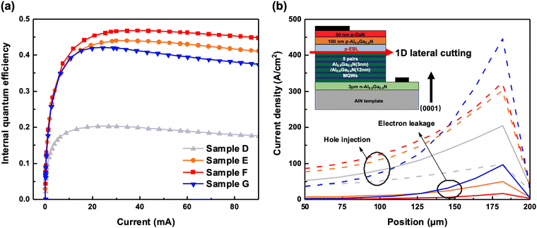
As illustrated in Fig. 1(a), the investigated LED architectures are grown on the c-plane AlN template. First, a 3 nm-Al0.6Ga0.4N (Si: 5 × 1018 cm−3) is grown as the electron injection layer. This layer is followed by five pairs of AlGaN/AlGaN multi-quantum wells (MQWs) comprising 12 nm Al0.6Ga0.4N quantum barriers and 3 nm Al0.5Ga0.5N quantum wells (QWs). Next, different SL-EBLs with 5 × 1018 cm−3 p-type doping are simulated for various electron blocking and hole injection capabilities, including a five-pair Alc1Ga1−c1N/Alc2Ga1−c2N SL-EBL. Considering that the EBL should possess a larger bandgap than the QW to block the electrons, the lower limit of the Al content of the barrier (c1) and well (c2) is set at 50%. The upper limit is 80%, depending on the growth and doping difficulty of AlGaN with a high Al content.27,28 The thickness of the barrier (t1) and well (t2) vary from 1 to 5 nm. Finally, 100 nm p-Al0.6Ga0.4N (Mg: 3 × 1019 cm−3) and 50 nm p-GaN (Mg: 1 × 1020 cm−3) are deposited as the hole injection layer and cap layer, respectively. The mesa size of the devices in the simulation is 300 μm × 300 μm, and the expected wavelength is 270 nm.
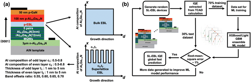 |
| | Fig. 1 (a) Cross-sectional diagram of light-emitting diode (LED) structures. (b) Workflow chart of the extreme gradient boosting (XGBoost) and light gradient boosting machine (LightGBM) stacked machine learning (ML) model prediction method. | |
In this study, the APSYS TCAD software by Crosslight is employed to consistently solve various physical equations and provide adequate data for ML.29 The operating temperature and background loss are set at 300 K and 2000 m−1, respectively.30,31 The auger recombination coefficient, Shockley–Read–Hall recombination lifetime, and radiative recombination coefficient are estimated respectively to be 2.88 × 10⁻³⁰ cm6 s−1, 15 ns, and 2.13 × 10⁻¹¹ cm3 s−1.32 The percentage of the polarization charge screened by the defects and carrier injection is set at 50%.33 The band offset ratios of AlGaN/AlGaN heterojunctions rely on material growth conditions and influence the simulation result. According to previous reports, diverse values from 0.55![[thin space (1/6-em)]](https://www.rsc.org/images/entities/char_2009.gif) :0.45 to 0.70:0.30 are considered in this work to offer a broad reference for the SL design.34 Other parameters are set as the default values in APSYS, so the results are reproducible by others.
:0.45 to 0.70:0.30 are considered in this work to offer a broad reference for the SL design.34 Other parameters are set as the default values in APSYS, so the results are reproducible by others.
Machine learning method for the superlattice electron blocking layer design
Data preparation.
Fig. 1(b) illustrates the workflow of the ML model construction. The ultraviolet (UV) LEDs with the various mentioned EBL designs are calculated using TCAD software. To build an efficient ML model, we split the TCAD calculation results into 70% for the training dataset and 30% for the testing dataset. The TCAD prediction requires substantial calculation resources; therefore, we used the try-and-catch method, where we first constructed the ML model with a small volume of TCAD calculation data and added more data from new calculations to enhance the ML model until the performance reached a specific criterion. The details of the parameters for the ML model are listed in Table 1.
Table 1 Parameters of the extreme gradient boosting (XGBoost)/light gradient boosting machine (LightGBM) stacked machine learning (ML) model
| Band offset |
Number of training data |
Number of testing data |
m
|
n
|
α
|
β
|
| 0.55 |
691 |
298 |
1 |
2 |
0.4359 |
0.4872/0.0769 |
| 0.6 |
416 |
180 |
2 |
1 |
0.1905/0.2381 |
0.5714 |
| 0.65 |
700 |
301 |
1 |
2 |
0.4536 |
0.5361/0.0103 |
| 0.7 |
465 |
200 |
2 |
1 |
0.4714/0.0143 |
0.5143 |
XGBoost/LightGBM stacking ensemble machine learning model.
ML is increasingly employed in semiconductor materials and devices for mechanism investigation and structure design. Recently, researchers used a neural network structure to predict the optical and electronic properties of semiconductor devices.35–39 Lin et al. applied a tree-based ensemble XGBoost model to predict the tunnel junction resistance and designed a novel asymmetrical tunnel junction with low resistance.40 In this paper, we propose a new ML framework for the SL-EBL design, which can predict the IQE with high accuracy. Instead of incurring a single model, we stacked two different existing methods in the training and testing process: XGBoost and LightGBM.41,42 In this framework, we use m XGBoost models and n LightGBM models and obtain results by stacking them. Given the ith sample's feature xi, we use fgj(xi) to denote the result of the jth XGBoost model with the corresponding weight αj, and flj(xi) to denote the result of the jth LightGBM model with the corresponding weight βj. Then, the final predicted result ŷi of the ith sample is given as follows:| |  | (1) |
The objective functions of XGBoost and LightGBM are the same. Both are inherited from the gradient boosting decision tree method, which is optimized iteratively, with the addition of a regularization term. Taking the XGBoost method as the example, given the corresponding features {x1,x2,…,xn} and prediction results {y1,y2,…,yn}, the objective function Obj(1) of the first iteration in XGBoost is as follows:
| |  | (2) |
where
is used to compute the difference between
yi and
fg(1)(
xi), and
Ω(
fg(1))(
xi) represents the regularization term constraining the parameters in the regression function
fg(1). Then, for the
tth iteration, we obtain the objective function Obj
(t) of XGBoost as follows:
| |  | (3) |
Then, after T iterations, we obtain the predicted IQE of the ith sample for the XGBoost method as  . The objective function for the LightGBM is the same as for XGBoost, which uses different optimization methods from XGBoost in the training process.
Evaluation of the proposed machine learning model
The RMSE values are calculated to illustrate the performance of the proposed ML model, which is relatively intuitive to the magnitude of IQE. The mathematical expression of RMSE is given as follows:| | 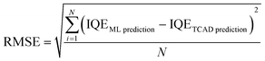 | (4) |
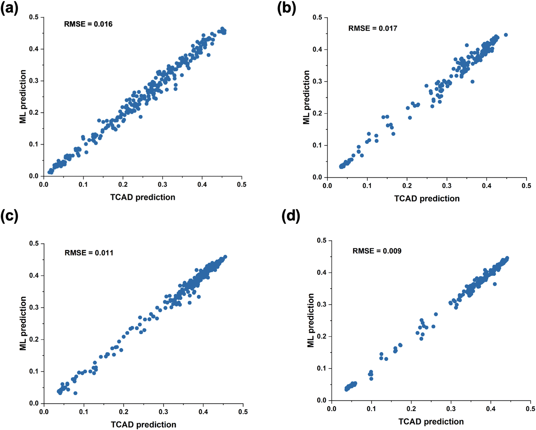
where N is the number of IQE data in the testing dataset. With this framework, we can combine XGBoost and LightGBM to predict the IQE, and their influence is controlled by the hyperparameters m, n, α, and β. Combining these two models makes this framework fit the training data better than the single model. In Fig. 2, IQEs from the ML prediction are compared to the IQE from the testing dataset, and the scatter points are well located along the line y = x, demonstrating the feasibility of the ML model. The regularization term in the objective function can overcome the overfitting problem well. The proposed models exhibit low RMSEs, which are 1.6%, 1.7%, 1.1%, and 0.9% for the band offsets of 0.55, 0.6, 0.65, and 0.7, respectively.
 |
| | Fig. 2 Internal quantum efficiency values from the machine learning (ML) prediction versus the TCAD prediction of the band offsets = (a) 0.55 (b) 0.6 (c) 0.65 and (d) 0.7. | |
Results and discussion
We plotted IQEs for changing c1 and c2 at an odd and even number of layer thicknesses and band offsets to better understand the results. The values for t1 and t2 increase from 1 to 5 nm with a step of 1 nm, and the band offsets vary from 0.55 to 0.7 with 0.05 intervals. The details for all figures are listed in the ESI.†
The ESI† provides Al compositions, thicknesses of odd and even-numbered layers, and the band offsets, which affect the performance of UV LEDs. Thus, a detailed investigation is conducted to understand the correlation between SL-EBL designs and UV LED performance.
Low Al-content superlattice electron blocking layer design from machine learning prediction
High p-type doping can be easily achieved with low Al content AlGaN because of the lower Mg activation energy, and the higher Al incorporation efficiency can facilitate epitaxy growth.43,44 Thus, predicting high-efficiency DUV LEDs with relatively low Al content, such as lower than 70%, is meaningful for practical devices. We selected a low Al-content SL-EBL (Sample A) from the predictions, which is compared to Al0.7Ga0.3N (Sample B) and Al0.8Ga0.2N (Sample C) bulk EBLs with the same total thickness. The compositions of the barrier and well are 0.70 and 0.58, and the thickness is 1 and 5 nm, respectively. The discussed band offset ratio is 0.6. All designs at different band offset ratios are presented in the ESI† and are not listed here.
Fig. 3(a) illustrates that Sample A has the highest IQE compared with Samples B and C, and the efficiency droop is also significantly suppressed. By appropriately designing the SL-EBL, DUV LEDs could perform better with less epitaxy difficulty. Using Fig. 3(b), we analyzed the electron and hole density lateral distribution at the interface between the EBL and MQWs, reflecting the electron leakage from MQWs to p-layers and hole injection from p-layers to MQWs. The figure reveals that Sample A has the lowest electron current, whereas Samples B and C face more serious electron leakage. Although Sample C has the highest hole current peak for the hole injection, Sample A has a more uniform hole current distribution along the mesa. Thus, the IQE improvement of the SL-EBL DUV LED can be concluded due to the better electron blocking and hole injection capability. Fig. 4 and Table 2 present the I–V curve and wall-plug efficiency (WPE) of Samples A, B, and C. Among the three structures, Sample C has the largest operating voltage due to the higher electron and hole potential from the high Al-content EBL, which compromises the WPE.
 |
| | Fig. 3 (a) Internal quantum efficiency curve of deep ultraviolet light-emitting diodes with bulk electron blocking layers (EBLs) and superlattice EBLs. (b) Electron and hole (dash line) current density versus lateral position at the interface between the EBL and MQWs. | |
 |
| | Fig. 4 (a) Current–voltage (I–V) curve and (b) wall-plug efficiency of deep ultraviolet light-emitting diodes with bulk electron blocking layers (EBLs) and superlattice EBLs. | |
Table 2 Operating voltage and wall-plug efficiency at 90 mA
|
|
Operating voltage (V) |
Wall-plug efficiency (%) |
| Notes: EBL: electron blocking layer; SL: superlattice |
| Al0.7Ga0.3N bulk EBL (Sample B) |
5.38 |
2.06 |
| Al0.8Ga0.2N bulk EBL (Sample C) |
5.70 |
3.03 |
| Al0.7Ga0.3N/Al0.58Ga0.42N SL-EBL (Sample A) |
5.52 |
3.48 |
The situation of Samples A and B is more complex. In the beginning, Sample A has a lower operating voltage (open voltage) than Sample B because the SL-EBL has a lower average Al content, leading to a lower potential difference. At the higher current, the operating voltage is higher in Sample A (5.52 V at 90 mA) compared with Sample B (5.38 V at 90 mA). The periodic barrier well structure of SL-EBL could confine carriers and block the carrier transport, corresponding to a higher voltage at the same current. Finally, Sample A presents the highest WPE (3.48% at 90 mA) because of the excellent IQE and medium operating voltage.
Composition design under different band offset ratios
From the data in the ESI,† it can be observed that the IQE highly depends on the composition of the SL-EBL. The highest IQE always occurs in the region where the SL-EBL possesses the Al0.8Ga0.2N SL barrier. The outcome is easily understood because the higher Al-content barrier can provide a stronger electron barrier to suppress electron leakage, and the polarization charge and band can be modulated by employing the SL well with different compositions. We investigate the influence of the SL composition on the IQE. The barrier composition is locked as 0.8 with well compositions of 0.5 (Sample D), 0.6 (Sample E), 0.7 (Sample F), and 0.8 (Sample G). The discussed thickness is t1 = t2 = 3 nm, and the band offset ratio is set to 0.6.
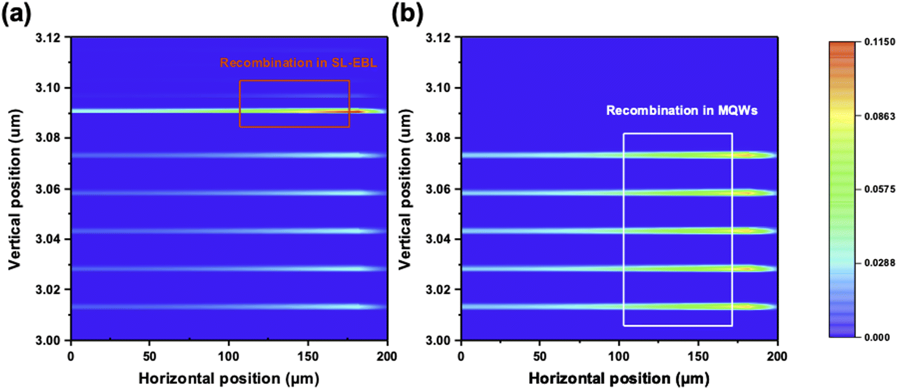
Fig. 5 depicts the calculated IQE curve for different samples. Sample F has the highest IQE, whereas Sample D has the lowest IQE and worse performance than the bulk EBL LED. The electron and hole lateral density distribution along the interface between MQWs and EBL is shown in Fig. 5(b). Sample F has the lowest electron leakage of all samples, and the hole injection is strong and uniform. However, Sample D suffers from poor carrier transport. Fig. 6 presents the radiative recombination rate distribution of Samples D and F to further illustrate the carrier transport deficiency in Sample D. In addition to the recombination in the MQWs, Sample D displays a strong recombination in the SL well. Due to the same composition as QWs, the SL wells play the role of extra QWs in UV LEDs. They are sandwiched between a higher Al-content barrier (Al0.8Ga0.2N), with stronger confinement for carriers. Thus, electrons in the MQWs prefer transferring to the SL and recombining with holes in the SL well. The recombination in the MQWs of Sample D is much weaker than that in Sample F, resulting in poor IQE.
 |
| | Fig. 5 (a) Internal quantum efficiency curve of samples. (b) Electron and hole current density versus lateral position at the interface between EBL and MQWs. | |
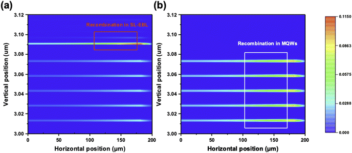 |
| | Fig. 6 Radiative recombination rate for (a) Sample D and (b) Sample F. | |
As mentioned, the band offset ratio of AlGaN significantly influences the carrier transport. Although the band offset ratio of AlGaN/AlGaN heterojunctions is normally considered as a fixed number under specific growth conditions, it can be modulated by the interfacial structure, defect position, interface states and Al content, which result from different epitaxy conditions.45 Thus, it is necessary to understand the influence of the band offset ratio on the SL-EBL design. In other words, the same design could not be directly transferred under dissimilar growth conditions. In Fig. 7, we set c1 to 0.8 and predict the IQE with various well-barrier composition differences. Furthermore, various band offset ratios and thicknesses are considered, revealing that the overall trends are similar regardless of the thickness of SL-EBLs. The IQE peak occurs at a larger composition difference when the band offset ratio increases, also shown in the ESI,† where generally the red region gradually shifts from the upper right corner to the upper left and lower right directions in the figures, indicating that the lower Al content of the SL well is desirable for improving the IQE. To explain this result, we use a trade-off model between polarization modulation and electron potential. As illustrated in Fig. 8, the electron potential is also lower at the lower band offset ratio due to the limited conduction band offset. Hence, the SL well should maintain a higher Al content to guarantee sufficient electron blocking capability. The electron potential is high enough for the larger band offset ratio, so it is better to use a low Al-content SL well to reduce the average Al content and modulate the polarization charge. We believe that this conclusion can significantly guide SL-EBL design.
 |
| | Fig. 7 Internal quantum efficiency (IQE) at 90 mA with various composition difference (c1 − c2) superlattice electron blocking layers at band offset ratios of t1 = t2 at (a) 2 nm, (b) 3 nm, (c) and 4 nm. | |
 |
| | Fig. 8 Theoretical model explaining the band offset ratio related to composition optimization. (a) High band offset leads to higher electron potential. (b) Low band offset leads to low electron potential between the multi-quantum well and superlattice electron blocking layer. | |
Thickness factors on superlattice electron blocking layer design
Fig. 9 presents the thickness influence on the IQE of the SL-EBL DUV LEDs under two well compositions. The optimal thickness simultaneously depends on the SL composition and band offset ratio. However, the IQE is compromised if the well and barrier are extremely thin, such as 1 and 2 nm, because of the poor electron blocking ability. In contrast, compared with the medium thickness area, a too-thick SL, such as 5 nm, has no obvious advantage in IQE.
 |
| | Fig. 9 (a) Thickness to internal quantum efficiency relationship for (a) c1 = 0.8 and c2 = 0.55 and (b) c1 = 0.8 and c2 = 0.65. | |
Moreover, a too-thick SL also leads to various problems. First, a too-thick SL can deteriorate the material quality because of the lattice mismatch. Second, p-type doping modulation is stronger in a short-period SL. Third, the operating voltage increases with the SL thickness, shirking the WPE and accumulating more heat. Thus, the first consideration of the design should focus on a medium region, such as a 3 nm average thickness.
Conclusions
In summary, to the best of our knowledge, a novel stacked XGBoost/LightGBM ML model is used to efficiently predict the UV LED IQE performance. The ML model is evaluated by its RMSEs and the low error values (around ∼1%), demonstrating that it is promising and accurate in terms of IQE predictions. Then, a systematic investigation of SL-EBL is conducted based on the ML model predictions, and a high-efficiency design can be achieved through the results. The improvement of IQE originates from the better electron blocking and hole injection, which were analyzed using the horizontal current distribution and radiative recombination rate. The optimized low Al-content SL-EBL is proposed to reduce epitaxy complexity, and it induces a nearly 70% IQE and WPE improvement compared with the Al0.7Ga0.3N bulk EBL. Furthermore, the physics mechanism of the SL-EBL was also systemically studied, including the influence of the composition, thickness, and band offset ratio. The composition difference between the SL well and barrier should be increased at larger band offset ratios, which can be explained by the trade-off between the electron potential and polarization modulation. The SL thickness is critical, and an average thickness of about 3 to 4 nm is recommended. We believe that the proposed ML method can also be applied in other LED structure investigations, and this study could deepen the understanding of the SL-EBL and guide the design theoretically and experimentally, boosting the development of high-efficiency DUV LEDs in the future.
Conflicts of interest
There are no conflicts to declare.
Acknowledgements
The KAUST authors would like to acknowledge the support from the KAUST Baseline Fund BAS/1/1664-01-01, Competitive Research Grant URF/1/3437-01-01, and the KAUST AI Initiative.
References
- M. Kneissl, T.-Y. Seong, J. Han and H. Amano, The Emergence and prospects of deep-ultraviolet light-emitting diode technologies, Nat. Photonics, 2019, 13, 233–244 CrossRef.
- H. Amano, R. Collazo, C. De Santi, S. Einfeldt, M. Funato, J. Glaab, S. Hagedorn, A. Hirano, H. Hirayama and R. Ishii, The 2020 Uv emitter roadmap, J. Phys. D: Appl. Phys., 2020, 53, 503001 CrossRef CAS.
- H.-Y. Ryu, I.-G. Choi, H.-S. Choi and J.-I. Shim, Investigation of light extraction efficiency in algan deep-ultraviolet light-emitting diodes, Appl. Phys. Express, 2013, 6, 062101 CrossRef.
- M. I. Hossain, Y. Itokazu, S. Kuwaba, N. Kamata, N. Maeda and H. Hirayama, Nonradiative recombination centers in deep Uv-wavelength algan quantum wells detected by below-gap excitation light, Jpn. J. Appl. Phys., 2019, 58, SCCB37 CrossRef CAS.
- C. Chu, K. Tian, H. Shao, J. Che, Y. Zhang and Z.-H. Zhang, Polarization self-screened multiple quantum wells for deep ultraviolet light-emitting diodes to enhance the optical power, IEEE Photonics J., 2021, 13, 1–5 Search PubMed.
- Y. Zhang, S. Krishnamoorthy, F. Akyol, J. M. Johnson, A. A. Allerman, M. W. Moseley, A. M. Armstrong, J. Hwang and S. Rajan, Reflective metal/semiconductor tunnel junctions for hole injection in algan Uv leds, Appl. Phys. Lett., 2017, 111, 051104 CrossRef.
- A. Pandey, J. Gim, R. Hovden and Z. Mi, Electron overflow of algan deep ultraviolet light emitting diodes, Appl. Phys. Lett., 2021, 118, 241109 CrossRef CAS.
- Z.-H. Zhang, J. Kou, S.-W. H. Chen, H. Shao, J. Che, C. Chu, K. Tian, Y. Zhang, W. Bi and H.-C. Kuo, Increasing the hole energy by grading the alloy composition of the P-type electron blocking layer for very high-performance deep ultraviolet light-emitting diodes, Photonics Res., 2019, 7, B1–B6 CrossRef CAS.
- Z.-H. Zhang, S.-W. Huang Chen, Y. Zhang, L. Li, S.-W. Wang, K. Tian, C. Chu, M. Fang, H.-C. Kuo and W. Bi, Hole transport manipulation to improve the hole injection for deep ultraviolet light-emitting diodes, ACS Photonics, 2017, 4, 1846–1850 CrossRef CAS.
- Z.-H. Zhang, S.-W. Huang Chen, C. Chu, K. Tian, M. Fang, Y. Zhang, W. Bi and H.-C. Kuo, nearly efficiency-droop-free algan-based ultraviolet light-emitting diodes with a specifically designed superlattice P-type electron blocking layer for high Mg doping efficiency, Nanoscale Res. Lett., 2018, 13, 1–7 CrossRef PubMed.
- W. Gu, Y. Lu, R. Lin, W. Guo, Z. Zhang, J.-H. Ryou, J. Yan, J. Wang, J. Li and X. Li, Baln for III-nitride Uv light-emitting diodes: Undoped electron blocking layer, J. Phys. D: Appl. Phys., 2021, 54, 175104 CrossRef CAS.
- Z. Liu, Y. Lu, Y. Wang, R. Lin, C. Xiong and X.-H. Li, Polarization modulation at last quantum barrier for high efficiency algan-based Uv led, IEEE Photonics J., 2021, 14, 8210208 Search PubMed.
- Z. Ren, Y. Lu, H.-H. Yao, H. Sun, C.-H. Liao, J. Dai, C. Chen, J.-H. Ryou, J. Yan and J. Wang, III-nitride deep Uv Led without electron blocking layer, IEEE Photonics J., 2019, 11, 1–11 Search PubMed.
- C. Chu, K. Tian, J. Che, H. Shao, J. Kou, Y. Zhang, Y. Li, M. Wang, Y. Zhu and Z.-H. Zhang, On the origin of enhanced hole injection for algan-based deep ultraviolet light-emitting diodes with aln insertion layer in P-electron blocking layer, Opt. Express, 2019, 27, A620–A628 CrossRef CAS PubMed.
- H. Yu, Z. Ren, H. Zhang, J. Dai, C. Chen, S. Long and H. Sun, Advantages of algan-based deep-ultraviolet light-emitting diodes with an al-composition graded quantum barrier, Opt. Express, 2019, 27, A1544–A1553 CrossRef CAS PubMed.
- Y.-H. Shih, J.-Y. Chang, J.-K. Sheu, Y.-K. Kuo, F.-M. Chen, M.-L. Lee and W.-C. Lai, Design of hole-blocking and electron-blocking layers in AlXGa1–X N-based Uv light-emitting diodes, IEEE Trans. Electron Devices, 2016, 63, 1141–1147 CAS.
- J. Verma, J. Simon, V. Protasenko, T. Kosel, H. Grace Xing and D. Jena, N-polar III-nitride quantum well light-emitting diodes with polarization-induced doping, Appl. Phys. Lett., 2011, 99, 171104 CrossRef.
- Y. Zhang, G. Deng, Y. Yu, Y. Wang, D. Zhao, Z. Shi, B. Zhang and X. Li, Demonstration of N-polar III-nitride tunnel junction led, ACS Photonics, 2020, 7, 1723–1728 CrossRef CAS.
- L. He, K. Zhang, H. Wu, C. He, W. Zhao, Q. Wang, S. Li and Z. Chen, Efficient carrier transport for 368 Nm ultraviolet leds with a P-alingan/algan short-period superlattice electron blocking layer, J. Mater. Chem. C, 2021, 9, 7893–7899 RSC.
- P. Sun, X. Bao, S. Liu, C. Ye, Z. Yuan, Y. Wu, S. Li and J. Kang, Advantages of algan-based deep ultraviolet light-emitting diodes with a superlattice electron blocking layer, Superlattices Microstruct., 2015, 85, 59–66 CrossRef CAS.
- E. F. Schubert, W. Grieshaber and I. Goepfert, Enhancement of deep acceptor activation in semiconductors by superlattice doping, Appl. Phys. Lett., 1996, 69, 3737–3739 CrossRef CAS.
- P. Kozodoy, Y. P. Smorchkova, M. Hansen, H. Xing, S. P. DenBaars, U. K. Mishra, A. Saxler and R. Perrin, β.; Mitchel, W., Polarization-enhanced Mg doping of algan/gan superlattices, Appl. Phys. Lett., 1999, 75, 2444–2446 CrossRef CAS.
- H. Tao, S. Xu, J. Zhang, P. Li, Z. Lin and Y. Hao, Numerical investigation on the enhanced performance of N-polar algan-based ultraviolet light-emitting diodes with superlattice P-type doping, IEEE Trans. Electron Devices, 2018, 66, 478–484 Search PubMed.
- B.-C. Lin, K.-J. Chen, H.-V. Han, Y.-P. Lan, C.-H. Chiu, C.-C. Lin, M.-H. Shih, P.-T. Lee and H.-C. Kuo, Advantages of blue leds with graded-composition algan/gan superlattice Ebl, IEEE Photonics Technol. Lett., 2013, 25, 2062–2065 CAS.
- Y.-A. Chang, Y.-R. Lin, J.-Y. Chang, T.-H. Wang and Y.-K. Kuo, Design and characterization of polarization-reversed alingan based ultraviolet light-emitting diode, IEEE J. Quantum Electron., 2013, 49, 553–559 CAS.
- Y.-K. Kuo, F.-M. Chen, J.-Y. Chang, M.-F. Huang, B.-T. Liou and Y.-H. Shih, Design and optimization of electron-blocking layer in deep ultraviolet light-emitting diodes, IEEE J. Quantum Electron., 2019, 56, 1–6 Search PubMed.
- M. Crawford, Materials challenges of algan-based Uv OPTOELECTRONIC DEVICEs, Semicond. Semimetals, 2017, 96, 3–44 CAS.
- K. Nam, M. Nakarmi, J. Li, J. Lin and H. Jiang, Mg acceptor level in Aln probed by deep ultraviolet photoluminescence, Appl. Phys. Lett., 2003, 83, 878–880 CrossRef CAS.
- Crosslight Software Inc., Crosslight APSYS User's Manual, 2018.
- T. Lu, S. Li, K. Zhang, C. Liu, Y. Yin, L. Wu, H. Wang, X. Yang, G. Xiao and Y. Zhou, Effect of the thickness of undoped gan interlayers between multiple quantum wells and the P-doped layer on the performance of gan light-emitting Diodes, Opt. Express, 2011, 19, 18319–18323 CrossRef CAS PubMed.
- V. Fiorentini, F. Bernardini and O. Ambacher, Evidence for nonlinear macroscopic polarization in III–V nitride alloy heterostructures, Appl. Phys. Lett., 2002, 80, 1204–1206 CrossRef CAS.
- J. Yun, J.-I. Shim and H. Hirayama, Analysis of efficiency droop in 280 Nm algan multiple-quantum-well light-emitting diodes based on carrier rate equation, Appl. Phys. Express, 2015, 8, 022104 CrossRef CAS.
- Y.-K. Kuo, J.-Y. Chang, F.-M. Chen, Y.-H. Shih and H.-T. Chang, Numerical investigation on the carrier transport characteristics of algan deep-Uv light-emitting diodes, IEEE J. Quantum Electron., 2016, 52, 1–5 Search PubMed.
- J. Piprek and Li, Z. Simon, Sensitivity analysis of electron leakage in III-nitride light-emitting diodes, Appl. Phys. Lett., 2013, 102, 131103 CrossRef.
- H. Dhillon, K. Mehta, M. Xiao, B. Wang, Y. Zhang and H. Y. Wong, Tcad-augmented machine learning with and without domain expertise, IEEE Trans. Electron Devices, 2021, 68, 5498–5503 CAS.
- T. Lu, V. Kanchi, K. Mehta, S. Oza, T. Ho and H. Y. Wong, Rapid mosfet contact resistance extraction from circuit using spice-augmented machine learning without feature extraction, IEEE Trans. Electron Devices, 2021, 68, 6026–6032 Search PubMed.
- R. Lin, Y. Zhai, C. Xiong and X. Li, Inverse design of plasmonic metasurfaces by convolutional neural network, Opt. Lett., 2020, 45, 1362–1365 CrossRef PubMed.
- R. Lin, Z. Alnakhli and X. Li, Engineering of multiple bound states in the continuum by latent representation of freeform structures, Photonics Res., 2021, 9, B96–B103 CrossRef.
- S. Lee, W. Choi, J. W. Park, D.-S. Kim, S. Nahm, W. Jeon, G. X. Gu, M. Kim and S. Ryu, Machine learning-enabled development of high performance gradient-index phononic crystals for energy focusing and harvesting, Nano Energy, 2022, 103, 107846 CrossRef CAS.
- R. Lin, P. Han, Y. Wang, R. Lin, Y. Lu, Z. Liu, X. Zhang and X. Li, low resistance asymmetric iii-nitride tunnel junctions designed by machine learning, Nanomaterials, 2021, 11, 2466 CrossRef CAS PubMed.
-
T. Chen and C. Guestrin In Xgboost: A Scalable Tree Boosting System, Proceedings of the 22nd acm sigkdd international conference on knowledge discovery and data mining, 2016; pp 785-794.
- G. Ke, Q. Meng, T. Finley, T. Wang, W. Chen, W. Ma, Q. Ye and T.-Y. Liu, Lightgbm: A highly efficient gradient boosting decision tree, Adv. Neural. Inf. Process. Syst., 2017, 30 Search PubMed.
- A. Kondratyev, R. Talalaev, W. Lundin, A. Sakharov, A. Tsatsul’nikov, E. Zavarin, A. Fomin and D. Sizov, Aluminum incorporation control in algan movpe: Experimental and modeling study, J. Cryst. Growth, 2004, 272, 420–425 CrossRef CAS.
- T. Kinoshita, T. Obata, H. Yanagi and S.-I. Inoue, High P-type conduction in high-Al content Mg-doped algan, Appl. Phys. Lett., 2013, 102, 012105 CrossRef.
- Y. Gao, D. Sun, X. Jiang and J. Zhao,
Ab initio analytic calculation of point defects in algan/gan heterointerfaces, J. Phys.: Condens. Matter, 2020, 33, 035002 CrossRef PubMed.
|
| This journal is © The Royal Society of Chemistry 2022 |
Click here to see how this site uses Cookies. View our privacy policy here. 
 Open Access Article
 This Open Access Article is licensed under a Creative Commons Attribution-Non Commercial 3.0 Unported Licence
 a,
Zhiyuan
Liu‡
a,
Peng
Han
b,
Ronghui
Lin
a,
Yi
Lu
a,
Haicheng
Cao
a,
Xiao
Tang
a,
Zhiyuan
Liu‡
a,
Peng
Han
b,
Ronghui
Lin
a,
Yi
Lu
a,
Haicheng
Cao
a,
Xiao
Tang


 is used to compute the difference between yi and fg(1)(xi), and Ω(fg(1))(xi) represents the regularization term constraining the parameters in the regression function fg(1). Then, for the tth iteration, we obtain the objective function Obj(t) of XGBoost as follows:
 . The objective function for the LightGBM is the same as for XGBoost, which uses different optimization methods from XGBoost in the training process.