
 Open Access Article
 This Open Access Article is licensed under a
 Creative Commons Attribution 3.0 Unported Licence
Insights into the degradation mechanism of carbene–metal–amide organic light-emitting diodes†
Campbell S. B.
Matthews
 a,
Alexander S.
Romanov
b and
Neil C.
Greenham
*a
a,
Alexander S.
Romanov
b and
Neil C.
Greenham
*a
aCavendish Laboratory, University of Cambridge, J.J. Thompson Avenue, Cambridge, CB3 0HE, UK. E-mail: ncg11@cam.ac.uk
bDepartment of Chemistry, University of Manchester, Oxford Road, Manchester, M13 9PL, UK
First published on 5th September 2022
Abstract
Organic light-emitting diodes (OLEDs) based on carbene–metal–amide (CMA) material are fabricated to investigate the fundamental processes that drive degradation in operational CMA OLEDs. The device lifetime of CMA OLEDs decreases rapidly with increased applied current density and implies a bimolecular degradation process. Photo- and electrical degradation studies of unipolar devices show that neither holes nor electrons are involved, and degradation is only driven by excitons. Probing of the recombination zone rationalises the degradation rate in OLEDs. We observe that the rate increases with the square of the exciton density and conclude that the degradation in CMA OLEDs is primarily driven by exciton–exciton annihilation.
Introduction
Organic light-emitting diodes (OLEDs) are a class of electroluminescent devices which demonstrate high efficiencies, tunable emission colour and ease of manufacture. While efficient red and green OLEDs demonstrate operational device lifetimes, LT50, (time taken to reduce to 50% of the initial brightness) of over 100![[thin space (1/6-em)]](https://www.rsc.org/images/entities/char_2009.gif) 000 hours, there are currently no deep blue organic emitters which simultaneously meet the industrial requirements of efficiency, brightness and device lifetime.1–3
000 hours, there are currently no deep blue organic emitters which simultaneously meet the industrial requirements of efficiency, brightness and device lifetime.1–3
One promising family of emitters for OLED applications is carbene–metal–amides (CMAs).4–8 CMAs are donor–bridge–acceptor organometallic molecules that emit through a thermally activated delayed fluorescence mechanism.6,9 One of the most studied CMAs is CMA1,7–15 which consists of a gold atom bridging a cyclic (alkyl)(amino) carbene and a carbazole ligand (Fig. 1). CMA1 OLEDs have been demonstrated with external quantum efficiencies above 25% and fabricated through either solution processing7 or physical vapour deposition.7,8 The luminescence from CMA1 is sky-blue, but modification of the carbazole with electron withdrawing groups such as aza, trifluoromethyl or cyano groups results in stabilisation of the HOMO energy level and deep-blue luminescence.10 The device lifetimes of CMA1 and its derivatives, however, are extremely short. For instance, CMA1 OLEDs have an LT95 device lifetime (time taken to reduce to 95% of the initial brightness) of only 2 hours at an initial brightness of 100 cd m−2. The deep blue CMA1 derivative OLEDs are even shorter-lived, with a LT50 of 10 to 32 minutes depending on the host material,10 indicating the need for further development of CMA OLEDs to improve the device lifetime. Understanding the degradation mechanism(s) in CMA OLEDs will ensure that the efforts of future work are directed most effectively.
 | ||
| Fig. 1 Chemical structures of CMA1 and materials used in OLEDs: TAPC, UGH2, TPBi and DCJTB. | ||
An operational OLED transports both an electron and a hole current to the emissive layer where the electrons and holes interact to form emissive excitons. The energies of electron–polaron, hole–polaron and exciton excited states are generally smaller (∼3 eV for deep blue emitters) than the dissociation energy of the covalent bonds in organic molecules. As such they are unlikely to directly cause irreversible degradation of the emissive materials in the absence of extrinsic chemical impurities. However, excited species can combine their energies through bimolecular annihilation to form a single high-energy (∼6 eV) state. The energy of such a state can allow the molecule to overcome the potential barrier for dissociation, resulting in bond breaking and the decomposition of the material.16 The fragmentation of molecules due to high-energy states formed through bimolecular annihilation has been identified as a major contributor to degradation in a large number of different OLED systems.1,17–19 The relatively long lifetime of triplet excitons increases the probability of bimolecular interactions, making triplet emitters particularly vulnerable to degradation through this pathway. Consequently the shorter device lifetimes seen in phosphorescent and TADF OLEDs compared to fluorescent OLEDs are often attributed to an increased rate of triplet–triplet annihilation.19,20 Polaron states can also be involved and exciton–polaron interactions have been identified as a possible source of degradation in OLEDs.21–24 In some blue TADF emitters the primary degradation mechanism has been specifically identified as originating from the interaction between an exciton and a hole. This was determined by measuring the degradation of a hole-only device under electrical and photo-excitation. The largest degree of degradation was seen only when both stresses were applied simultaneously. When applied independently, the degradation is negligible or much less. Further tests in electron-only devices showed that exciton–electron interactions did not contribute to degradation.21,22
In this work the degradation of CMA1 is studied by independently replicating the various stresses experienced inside an operational OLED. Unipolar devices are fabricated in order to test the degradation caused by a current of either electrons or holes. Photoexcitation is used to generate a population of excitons without the presence of electrons or holes. Measuring the degradation induced by each excited species, or the different combinations thereof, will indicate the stability of CMA1 to each species, or provide an insight towards a bimolecular degradation.
Results and discussion
In some OLEDs it has been identified that the primary degradative pathway is linked to the host molecule.25,26 CMA1 exhibits minimal luminescence self-quenching and can be used in OLEDs without the need for a host matrix.8 CMA1 is therefore studied exclusively in neat films so as to avoid any degradative effects from the host. The degradation behaviour of CMA1 OLEDs is first established. OLEDs were fabricated using physical vapour deposition under high vacuum (<2.6 × 10⁻⁶ mbar). Films were deposited at rates of 0.1 to 2.0 Å s−1 onto indium-tin oxide (ITO) coated glass substrates with a sheet resistance of 15 Ω□−1. The device structure consists of a 40 nm thick hole transport layer of 1,1-bis[(di-4-tolylamino)phenyl]cyclohexane (TAPC), a 20 nm thick emissive layer of CMA1, a 10 nm thick hole-blocking layer of 1,4-phenylenebis(triphenylsilane) (UGH2) doped at 10 vol% with 2,2′,2′′-(1,3,5-benzinetriyl)-tris(1-phenyl-1-H-benzimidazole) (TPBi) and a 40 nm thick electron-transporting layer of TPBi. The electrodes consisted of a 1 nm thick layer of lithium fluoride and 100 nm thick layer of aluminium. The chemical structures of the materials used are shown in Fig. 1.The device lifetimes were determined by applying a constant current density, J, and measuring the reduction in luminance. Devices were tested in an inert nitrogen environment in order to avoid chemical degradation by the atmosphere. The LT50 corresponds to the time taken to reduce to 50% of the initial brightness. The luminance decay for different current densities is shown in Fig. 2A and the LT50 values as a function of current density are shown in Fig. 2B. The relationship between device lifetime and current density is linear in log–log space with a gradient of −1.42, which implies a power law relationship of the form LT50 ∝ J−1.42.
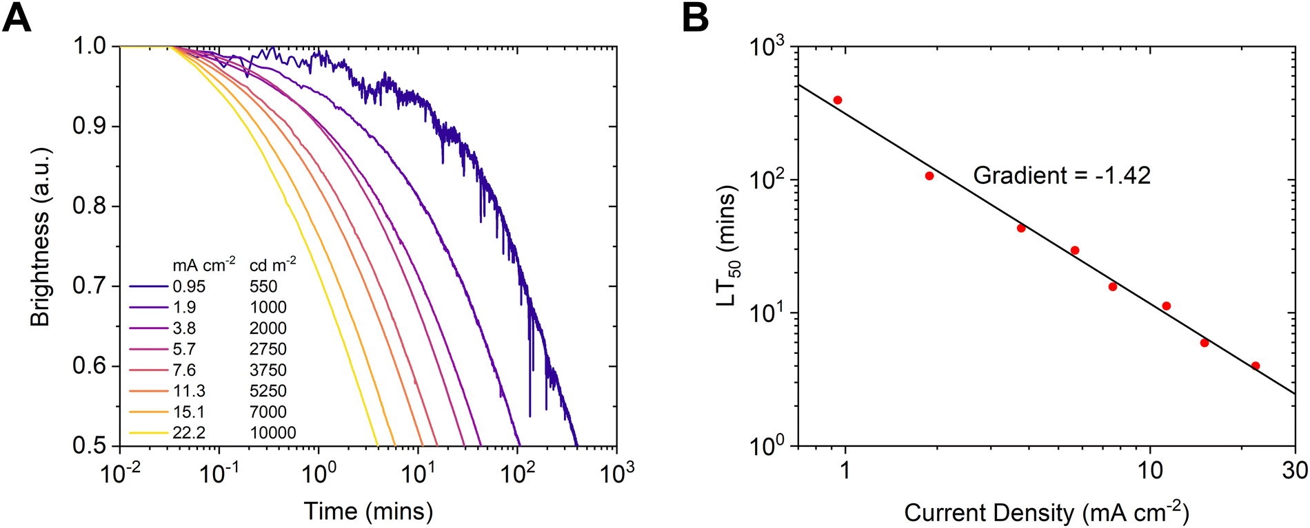 | ||
| Fig. 2 (A) device lifetime measurements of OLEDs. (B) LT50 of OLEDs as a function of current density. | ||
For a purely monomolecular process, the device lifetime should be inversely proportional to the current density (e.g. if the number of excited states is doubled then the lifetime is halved). In contrast bimolecular degradation depends on the excited state density, due to the increased chance of two states coming into contact.27 In the simplest case where the excited state density is proportional to the current density, the lifetime should scale with J−2. The relationship between charge density and current density, however, can be non-linear and exciton-polaron interactions may scale at a lower rate. To investigate whether excitons and polarons are interacting in a destructive manner, unipolar devices are fabricated and the degradation studied under different stresses.
The unipolar devices are fabricated onto ITO-coated glass substrates using physical vapour deposition. Electron-only devices consisted of a spin coated layer of ZnO nanoparticles, a 50 nm thick layer of CMA1, a 1 nm thick layer of LiF and 100 nm thick layer of Al. The hole-only devices consisted of a 1 nm thick layer of MoO3, 50 nm thick layer of CMA1, a 10 nm thick layer of MoO3 and 100 nm Al.
The unipolar devices do not produce electroluminescence. Instead the reduction in photoluminescence intensity is measured as a function of time using photo excitation from a 405 nm laser. A series of different conditions can then be investigated. Current can be passed through the electron-only and hole-only devices to test degradation exclusively from polarons. The laser is only applied to the device for short periods (∼10 s) to measure the photoluminescence and avoid photoinduced degradation as much as possible. The applied current density, 1.9 mA cm−2, is the same as that applied to OLEDs for an initial brightness of 1000 cd m−2 and is turned off during the photoluminescence measurements. Degradation caused by excitons can also be measured by continuously photoexciting the devices while no current is flowing. Photoexcitation is provided by a constant 10 mW cm−2 from a 405 nm laser. The bimolecular interaction between a polaron and an exciton can be tested by applying both electric current and photoexcitation at the same time. Any degradation caused by the interaction of excitons and holes or excitons and electrons can be separately deduced from the hole-only and electron-only devices respectively.
The photoluminescence intensity as a function of time is shown in Fig. 3. Under either an electron-only or a hole-only current, CMA1 does not show any reduction in photoluminescence. A reduction in brightness is, however, observed under constant photoexcitation. The extent of the luminance loss is not changed when combined with an applied electron-only or hole-only current. The loss in luminance is not driven by polaron states, either alone or when interacting with exciton states.
 | ||
| Fig. 3 Degradation of (A) electron-only and (B) hole-only devices under different combinations of 405 nm photoexcitation and a current density of 1.9 mA cm−2. | ||
Degradation is only caused by photoexcitation and implies that the degradation process is dependent on exciton–exciton interactions. In such a case a LT50 ∝ J−2 behaviour would have been expected. It is possible, however, that the recombination zone widens or narrows with increased current density and could explain the LT50 ∝ J−1.42 relationship observed in OLEDs.
Sensitized devices are fabricated in order to investigate the nature of the recombination zone in the CMA1 OLEDs. A thin strip of the emissive layer is doped with a sensitizer; an emissive molecule which has HOMO/LUMO levels within that of CMA1. Excitons preferentially form on, or transfer to, the sensitizer. Luminescence from the sensitizer is then observed as a red peak that can be distinguished from the CMA1 emission. The sensitized strip can be placed at different locations within the emissive layer. The relative intensities of the red peak as a function of sensitizer strip location provide a measure of the relative exciton generation rate at each location.
Fig. 4 shows a schematic of the sensitized OLED structure. The overall structure is the same as the regular CMA1 OLEDs, except that the emissive layer is broken into eight 2.5 nm thick strips, one of which is doped at 1 vol% with the sensitizer 4-(dicyanomethylene)-2-tert-butyl-6-(1,1,7,7-tetramethyljulolidin-4-ylvinyl)-4H-pyran (DCJTB, Fig. 1). The sensitized OLEDs are numbered 1 through 8 which corresponds to the location of the sensitizer strip, beginning from the hole-injecting side (TAPC layer).
 | ||
| Fig. 4 Sensitized OLED schematic with HOMO and LUMO energy levels (in eV). | ||
The electrical characteristics of the sensitized OLEDs show little change from the regular CMA1 OLEDs (see Fig. S4, ESI†) which implies that the insertion of the sensitizer strip has not affected the recombination zone. In contrast, the electroluminescence, shown in Fig. 5A, contains two peaks which vary in relative intensity. The green peak at around 510 nm corresponds to the CMA1, while the red peak at about 585 nm corresponds to DCJTB. The relative intensity of DCJTB emission increases the closer the sensitizer strip is to the electron-injecting side (CMA1:UGH2 interface). The relative contribution to the electroluminescence from the sensitizer can be calculated by making a weighted subtraction with the electroluminescence from the reference CMA1 OLED. The contribution from DCJTB is proportional to the relative exciton density, and the corresponding recombination zone profile is shown in Fig. 5B.
 | ||
| Fig. 5 (A) Electroluminescence of sensitized devices at a current density of 1 mA cm−2, (B) relative exciton density across the emissive layer. | ||
The exciton density is higher at the electron injecting side than the hole injecting side. At the lower current densities over half of the excitons are generated within 5 nm of the CMA1:UGH2 layer interface. The recombination zone is very narrow and drives a significant amount of bimolecular interactions. The profile of the recombination zone also changes with current density and becomes more uniform at higher current densities. The current density and exciton density are therefore not proportional and this explains why the device lifetime scales less steeply than J−2.
To further study the behaviour of CMA1 due to exciton interactions, films of neat CMA1 were subjected to photoexcitation at different power densities. The applied power density is proportional to the generated exciton density (see Fig. S5, ESI†). The reduction in photoluminescence intensity can be monitored and an LT85 derived which corresponds to when the photoluminescence reduces to 85% of the initial brightness. Fig. 6A shows the luminance decay of 50 nm thick CMA1 films subject to photoexcitation from a 405 nm laser at different power densities. The LT85 values as a function of power density are shown in Fig. 6B. At higher power densities the trend in log–log space is linear with a gradient of −2, which is expected for a bimolecular process. The trend tails off at lower power densities and the gradient reduces to −1.27, which may suggest an additional weaker contribution from some secondary process.
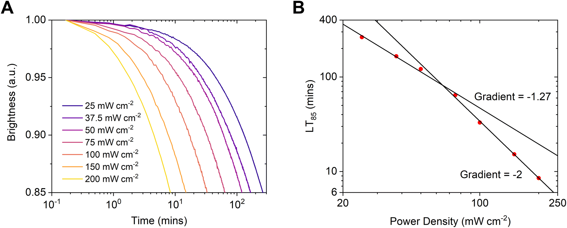 | ||
| Fig. 6 (A) degradation of CMA1 films under 405 nm photoexcitation, (B) LT85 lifetimes as a function of incident power density. | ||
Considering the applied current density and the recombination zone profile from Fig. 5B, the bimolecular dependence in Fig. 6B corresponds to the exciton densities in OLEDs operating at an initial brightness of 500 cd m−2 or more. A bimolecular process is therefore driving degradation in OLEDs at useful brightnesses, although a weaker monomolecular process may also be occurring, but only becomes apparent at lower exciton densities.
Conclusions
The relationship between the device lifetime of CMA1 OLEDs and current density implies that degradation is caused by a bimolecular interaction. The degradation tests of unipolar devices show that only excitons induce degradation in CMA1 and that polarons are not involved. The luminance loss in films shows an inverse square dependence at higher power densities indicating that degradation is primarily caused by a bimolecular exciton–exciton interaction. At lower power densities the trend diverges suggesting a secondary weaker, monomolecular process also occurs, however it is less relevant under practical operating conditions.Our work suggests that increased device lifetime in CMA OLEDs could be achieved by minimising exciton–exciton annihilation. Reduction of the exciton density in devices by flattening the recombination zone could provide some improvement in device lifetime. To achieve this it would be necessary to improve transport of electrons in the emissive layer so that excitons are more likely to form throughout the entire thickness of the layer and not be concentrated at the interface with the hole blocking layer. Increasing the thickness of the emissive layer may also help to distribute excitons and reduce the local exciton density. Finally, materials design of deep-blue light emitters28,29 would aid further to reduce the excited state lifetime and exciton–exciton annihilation rate. To make significant improvements, however, more stable CMA variants must be synthesised with a focus on stabilisation of the excited state or reduced susceptibility to degradative exciton–exciton interactions.
Author contributions
C. S. B. M. fabricated the devices and films and conducted the experiments and analysis; A. S. R. synthesised the CMA1 material. All authors contributed to writing of the manuscript.Conflicts of interest
There are no conflicts to declare.Acknowledgements
C. S. B. M. acknowledges support from St John's College, Cambridge; the Royal Society (grant no. RGF\EA\180041) and the Cambridge Philosophical Society; A. S. R. acknowledges support from the Royal Society (grant no. URF\R1\180288 and RGF\EA\181008). This work was supported by the EPSRC (Grant EP/M005143/1). The data underlying this paper is available at the following web link: https://doi.org/10.17863/CAM.86858.Notes and references
- J. H. Lee, C. H. Chen, P. H. Lee, H. Y. Lin, M. K. Leung, T. L. Chiu and C. F. Lin, J. Mater. Chem. C, 2019, 7, 5874–5888 RSC.
- S. Sudheendran Swayamprabha, D. K. Dubey, Shahnawaz, R. A. K. Yadav, M. R. Nagar, A. Sharma, F. C. Tung and J. H. Jou, Adv. Sci., 2021, 8, 2002254 CrossRef CAS PubMed.
- A. Monkman, ACS Appl. Mater. Interfaces, 2021, 14, 20463–20467 CrossRef.
- R. Hamze, J. L. Peltier, D. Sylvinson, M. Jung, J. Cardenas, R. Haiges, M. Soleilhavoup, R. Jazzar, P. I. Djurovich, G. Bertrand and M. E. Thompson, Science, 2019, 363, 601–606 CrossRef CAS PubMed.
- T. Yi Li, D. G. Shlian, P. I. Djurovich and M. E. Thompson, Chem. – Eur. J., 2021, 27, 6191–6197 CrossRef.
- R. Hamze, M. Idris, M. R. Daniel Sylvinson, M. Chul Jung, R. Haiges, P. I. Djurovich and M. E. Thompson, Front. Chem., 2020, 8, 401 CrossRef CAS.
- D. Di, A. S. Romanov, L. Yang, J. M. Richter, J. P. H. Rivett, S. Jones, T. H. Thomas, M. A. Jalebi, R. H. Friend, M. Linnolahti, M. Bochmann and D. Credgington, Science, 2017, 356, 159–163 CrossRef CAS PubMed.
- P. J. Conaghan, S. M. Menke, A. S. Romanov, S. T. E. Jones, A. J. Pearson, E. W. Evans, M. Bochmann, N. C. Greenham and D. Credgington, Adv. Mater., 2018, 30, 1802285 CrossRef PubMed.
- A. S. Romanov, S. T. E. Jones, Q. Gu, P. J. Conaghan, B. H. Drummond, J. Feng, F. Chotard, L. Buizza, M. Foley, M. Linnolahti, D. Credgington and M. Bochmann, Chem. Sci., 2020, 11, 435–446 RSC.
- P. J. Conaghan, C. S. B. Matthews, F. Chotard, S. T. E. Jones, N. C. Greenham, M. Bochmann, D. Credgington and A. S. Romanov, Nat. Commun., 2020, 11, 1758 CrossRef CAS PubMed.
- J. Feng, E. J. Taffet, A. P. M. Reponen, A. S. Romanov, Y. Olivier, V. Lemaur, L. Yang, M. Linnolahti, M. Bochmann, D. Beljonne and D. Credgington, Chem. Mater., 2020, 32, 4743–4753 CrossRef CAS.
- J. Feng, L. Yang, A. S. Romanov, J. Ratanapreechachai, A. M. Reponen, S. T. E. Jones, M. Linnolahti, T. J. H. Hele, A. Köhler, H. Bässler, M. Bochmann and D. Credgington, Adv. Funct. Mater., 2020, 30, 1908715 CrossRef CAS.
- C. R. Hall, A. S. Romanov, M. Bochmann and S. R. Meech, J. Phys. Chem. Lett., 2018, 9, 5873–5876 CrossRef CAS PubMed.
- S. Thompson, J. Eng and T. J. Penfold, J. Chem. Phys., 2018, 149, 014304 CrossRef CAS.
- J. Föller and C. M. Marian, J. Phys. Chem. Lett., 2017, 8, 5643–5647 CrossRef.
- N. Nakashima and K. Yoshihara, J. Phys. Chem., 1989, 93, 7763–7771 CrossRef CAS.
- S. Scholz, D. Kondakov, B. Lüssem and K. Leo, Chem. Rev., 2015, 115, 8449–8503 CrossRef CAS.
- N. C. Giebink, B. W. D’Andrade, M. S. Weaver, P. B. Mackenzie, J. J. Brown, M. E. Thompson and S. R. Forrest, J. Appl. Phys., 2008, 103, 044509 CrossRef.
- D. Jacquemin and D. Escudero, Chem. Sci., 2017, 8, 7844–7850 RSC.
- C. Murawski, K. Leo and M. C. Gather, Adv. Mater., 2013, 25, 6801–6827 CrossRef CAS PubMed.
- L. S. Cui, Y. L. Deng, D. P. K. Tsang, Z. Q. Jiang, Q. Zhang, L. S. Liao and C. Adachi, Adv. Mater., 2016, 28, 7620–7625 CrossRef CAS PubMed.
- J. Sohn, D. Ko, H. Lee, J. Han, S. D. Lee and C. Lee, Org. Electron., 2019, 70, 286–291 CrossRef CAS.
- D. P. K. Tsang and C. Adachi, Sci. Rep., 2016, 6, 1–10 CrossRef PubMed.
- Y. Zhang, J. Lee and S. R. Forrest, Nat. Commun., 2014, 5, 5008 CrossRef CAS PubMed.
- S. Kim, H. J. Bae, S. Park, W. Kim, J. Kim, J. S. Kim, Y. Jung, S. Sul, S. G. Ihn, C. Noh, S. Kim and Y. You, Nat. Commun., 2018, 9, 1211 CrossRef PubMed.
- A. S. D. Sandanayaka, T. Matsushima and C. Adachi, J. Phys. Chem. C, 2015, 119, 23845–23851 CrossRef CAS.
- S. R. Forrest, Organic Electronics: Foundations to Applications., Oxford University Press, USA, 2020 Search PubMed.
- A.-P. M. Reponen, F. Chotard, A. Lempelto, V. Shekhovtsev, D. Credgington, M. Bochmann, M. Linnolahti, N. C. Greenham and A. S. Romanov, Adv. Opt. Mater., 2022, 10, 2200312 CrossRef CAS.
- Q. Gu, F. Chotard, J. Eng, A.-P. M. Reponen, I. J. Vitorica-Yrezabal, A. W. Woodward, T. J. Penfold, D. Credgington, M. Bochmann and A. S. Romanov, Chem. Mater., 2022, 34, 7526–7542 CrossRef CAS.
Footnote |
| † Electronic supplementary information (ESI) available. See DOI: https://doi.org/10.1039/d2tc02288e |
| This journal is © The Royal Society of Chemistry 2022 |