
 Open Access Article
 This Open Access Article is licensed under a Creative Commons Attribution-Non Commercial 3.0 Unported Licence
A facile route to fabricating a crack-free Mg0.99Cu0.01Ag0.97Sb0.99/graphene/PEDOT:PSS thermoelectric film on a flexible substrate†
Yanan
Wang
ab,
Raju
Chetty
*a,
Zihang
Liu
a,
Longquan
Wang
ab,
Takeo
Ohsawa
c,
Weihong
Gao
a and
Takao
Mori
 *ab
*ab
aInternational Center for Materials Nanoarchitectonics (WPI-MANA), NIMS, 1-1 Namiki, Tsukuba, Ibaraki 305-0044, Japan. E-mail: MORI.Takao@nims.go.jp; CHETTY.Raju@nims.go.jp
bGraduate School of Pure and Applied Sciences, University of Tsukuba, 1-1-1 Tennodai, Tsukuba, Ibaraki 305-8577, Japan
cResearch Center for Functional Materials, NIMS, 1-1 Namiki, Tsukuba, Ibaraki 305-0044, Japan
First published on 29th July 2022
Abstract
Organic/inorganic hybrid synthesis methods are effective for fabricating flexible thermoelectric (TE) films and devices. In the present study, a flexible Mg0.99Cu0.01Ag0.99Sb0.97/graphene/PEDOT:PSS (MCAS/G/P) TE film was prepared on a polytetrafluoroethylene (PTFE) substrate. A physical process was developed to resolve the cracking problem during the hybrid process. In this hybrid structure, MCAS particles constitute a matrix, while a conductive network formed by graphene and PEDOT:PSS reduces the interfacial contact resistance between MCAS particles, thereby facilitating carrier transport and in turn enhancing the electrical properties of the hybrid films. The graphene content in the MCAS/x wt% G/P hybrid system was optimized by evaluating the TE properties, which reveals that the optimum content of graphene is 40 wt%. Furthermore, the influence of a hybrid mass fraction on both the TE properties and mechanical flexibility of the ternary hybrid film was systematically investigated. As a result, a maximum power factor (PF) of 31 μW m−1 K−2 was obtained at a 93.8 wt% powder ratio. However, mechanical bending tests revealed that a maximum PF of 16 μW m−1 K−2 was obtained for the flexible MCAS/G/P film loaded with 88.3 wt% MCAS/G. The hybrid synthesis method proposed in this work may pave the way for a design strategy in the fabrication of novel material-based flexible TE films and spur the emerging application of new hybrid flexible materials in energy harvesting.
1. Introduction
With the advancement in flexible electronic technology, much attention has been paid to thermal management, which can effectively utilize low-grade waste heat for electrical power generation.1 Thermoelectric (TE) materials, which are one of the prominent energy harvesting technologies, can directly convert the unutilized heat into electrical energy.2–6 Recently, the potential application of TE materials in flexible device technology for harvesting waste heat has increased.7–10 The conversion efficiency of the TE device is defined by the material's thermoelectric figure of merit, expressed as ZT = S2σT/κtotal, where S, σ, κtotal, and T stand for the Seebeck coefficient, the electrical conductivity, the total thermal conductivity, and the absolute temperature, respectively. The maximum output power of TE materials is indicated by a parameter called the power factor, PF = S2σ, which is usually used to assess the performance of TE films.8 In recent decades, advancements in controlling the electron and phonon transport by various novel approaches11–15 resulted in a substantial improvement in ZT for various inorganic TE materials16–22 with high conversion efficiencies.23–27Despite the high thermoelectric performance of inorganic TE materials, the rigidity limits their potential use in wearable thermoelectric technology.28,29 Therefore, the research has been focused on the development of flexible TE (FTE) materials and devices.7,9,10 Mostly, the state-of-art TE materials based on Bi2Te3 are explored as high-performance FTE devices. For example, Wang et al. reported an organic/inorganic hybrid design route to enhance the ZT value of Bi0.5Sb1.5Te3 (BST) from 0.7 to 1.1 by incorporating copper(II) phthalocyanine (CuPc) at grain boundary of BST as temperature varying from 300 K and 523 K.30 Ao et al. reported n-type Te-embedded Bi2Te3 flexible thin films based on a flexible polyimide substrate with an ultrahigh room-temperature PF of 14.65 μW cm−1 K−2.31 Besides, Norimasa et al. overcame the flexible substrate shrinking problem during the process of film deposition and reported a flexible Bi2Te3 thin film by sputtering deposition and the post-thermal annealing method with improved TE properties.32 Although Bi–Te alloy-related materials show excellent TE properties, Te is rare, toxic, and expensive, which restricts their applicability in wearable or embeddable devices. Therefore, it is highly essential to develop FTE devices, which are Te free and contain less toxic elements. Recently, through novel fabrication technologies and rational structure design, n-type Ag2Se-based films with high thermoelectric properties targeting commercialization have been demonstrated,33–35 which invokes the motivation to improve the performance of the existing TE materials by different optimizing technologies.
Since 2012, α-MgAgSb has been paid much attention as a promising p-type thermoelectric material for power generation below 550 K.36–38 α-MgAgSb possesses several advantages such as degenerate semiconducting behavior, intrinsically low lattice thermal conductivity, and good mechanical properties. Zhao et al. reported the pioneering research work on α-MgAgSb with enhanced thermoelectric properties by optimizing the processing technology and acceptor doping.37 A maximum ZT of ∼1.4 at 450 K was reported for Ni-doped MgAg0.97Sb0.99 compounds. Thereafter, extensive research has been focused on tuning the hole carrier concentration by several acceptor doping elements on the Mg/Ag site to optimize the electrical and thermal properties of α-MgAgSb.39–52 Moreover, α-MgAgSb showed not only excellent TE properties but also a maximum conversion efficiency, ηmax, of 8.5% for a single TE leg was demonstrated at a temperature difference (ΔT) of 225 K.38 Recently, thermoelectric modules fabricated based on n-type Mg3(Sb,Bi)2 and p-type α-MgAgSb compounds demonstrated high conversion efficiencies, which rival those of Bi2Te3-based compounds.53–55 For example, a high ηmax of 7.3% was achieved in the Mg3Sb2/MgAgSb-based 8-pair module at a ΔT of 315 K.53 A Mg3(Sb,Bi)2/MgAgSb-based 2-pair module showed an ηmax of 6.5% at a ΔT of 250 K.54 An ηmax of 2.8% at a ΔT of 95 K was obtained for the Mg3.2Bi1.5Sb0.5/MgAgSb-based 8-pair module.55 To date, despite the high ZT and module performances of α-MgAgSb compounds, there have been no reports on the development of flexible thermoelectric materials and/or devices.
Herein, we focused on the development of FTE films based on α-MgAgSb to explore them as a potential candidate for room temperature TE applications. An organic–inorganic strategy9,30,56,57 and an extended approach reported in our previous study are used in the present work.58 In brief, we used a chemical composition of Mg0.99Cu0.01Ag0.97Sb0.99 which possesses a broad temperature plateau of ZT above unity as the inorganic matrix,53 and formed a hybrid material with poly(3,4-ethylenedioxythiophene):poly(4-styrenesulfonate) (PEDOT:PSS). PEDOT:PSS, among the conductive polymers, is the most promising material due to its advantages of water-dispersibility, good conductivity, low-cost, high transparency, and excellent processability.59 Over the last few decades, the development of PEDOT:PSS has opened the doors for its applications in a wide range of communities spanning from antistatic coatings to energy conversion and energy storage devices.60–64 Nowadays, the potential applications of PEDOT:PSS based materials are still explored and studied in new domains such as flexible TE materials,59 thin film transparent heaters65 or bioelectronics,66,67etc. In this study, PEDOT:PSS is anticipated to form a conductive network in the MCAS matrix to bridge the neighboring particles by forming conductive paths and enhance the flexibility of the TE film because of its beneficial characteristics, especially its p-type TE properties, intrinsic high mechanical flexibility, and excellent thermal stability.68–71 However, it was found that there is a new challenge of cracking (see Fig. S1, ESI†) in the MCAS/PEDOT:PSS hybrid system including the high interfacial resistance that has to be addressed to enhance σ, and therefore the PF (S2σ). Accordingly, Zhang et al. optimized interfacial carrier transport by removing the potential oxidation layer on the surface of Bi2Te3.72 Wang et al. coated the highly conductive CuTe layer on Bi0.5Sb1.5Te3, reaching a promising σ of ∼2300 S cm−1.73 Also, in our previous work,58 graphene was added into the hybrid system of Cu0.98Zn0.02FeS2/PEDOT:PSS leading to a simultaneous enhancement of the electrical conductivity and flexibility of the resultant films. Specifically, graphene, with a single atomic layer of covalently bonded carbon atoms in a honeycomb lattice,74 possesses high mechanical strength75 and electrical transport to accommodate the change of MCAS particles during the flexibility test.76 Moreover, as a zero-bandgap semi-metal material, it can exhibit an exceptional charge carrier mobility.77 Therefore, graphene is an ideal candidate to bridge the interface between organic and inorganic materials for optimizing the carrier transport and the flexibility in the hybrid system.
Accordingly, we developed a facile method to resolve the cracking of Mg0.99Cu0.01Ag0.97Sb0.99/PEDOT:PSS film. For enhancing σ, and thus the PF, graphene was strategically hybridized to optimize the carrier transport as well as improve the flexibility of the hybrid films. Moreover, to optimize the flexibility, the σ, S, and PF of hybrid films were systematically studied as a function of the mass fraction of inorganic materials.
2. Experimental methods
2.1 Materials
High purity elements of Mg turnings (99.95%, Sigma Aldrich), Cu beads (99.9995%, Sigma Aldrich), Ag shots (≥99.99%, Sigma Aldrich) and Sb chunks (99.999%, 5N plus) were used for the preparation of Mg0.99Cu0.01Ag0.97Sb0.99. The PEDOT:PSS solution (Heraeus Clevios TM PEDOT:PSS PH1000, 1.3 wt % in water) was obtained from As One. Ethanol (C2H5OH, 98%) was purchased from Wako chemicals. Graphene nanoplatelets (6–8 nm thick × 15 μm wide), polyethylene terephthalate (PET, 0.013 mm in thickness), and the polytetrafluoroethylene (PTFE) membrane (0.025 μm pore size, 25 mm and 47 mm in diameter) were purchased from Sigma Aldrich.2.2 Synthesis of the Mg0.99Cu0.01Ag0.97Sb0.99 (MCAS) powder
The synthesis process of MCAS was followed according to our previous report.37,53 Briefly, high-purity raw elements were directly weighed according to the nominal composition of MCAS, subsequently carried out by the two-step high-energy ball milling method: first, Mg, Ag, and Cu according to the designed ratio were loaded into a stainless steel jar in an argon-filled glove box, followed by ball milling for 10 hours; next, Sb chunks were added to the ball milled mixture and then ball milled for another 8 hours; finally, the resultant powder was sintered using spark plasma sintering (SPS, SPS-1080 System, SPS SYNTEX INC) at 583 K for 10 minutes to obtain high-density disks. After checking the properties, the disks were loaded in the stainless-steel ball milling jar in the glovebox, and subjected to a high-energy mill (8000D Mixer/Mill in which the grinding vial is horizontally shaken vigorously at 1060 cycles per minute (cpm)@60 Hz, 115 V) with a ball (diameter of 12.7 mm)-to-powder ratio of 32![[thin space (1/6-em)]](https://www.rsc.org/images/entities/char_2009.gif) :3 for 5 minutes to obtain the fine powder.
:3 for 5 minutes to obtain the fine powder.
2.3 Synthesis of MCAS/G/P films
Considering that the agglomeration of graphene during the process will limit its functionality in improving the TE properties of hybrids,78,79 herein, initially, the graphene was first ball milled with the MCAS powder to get good dispersion meanwhile wrapping the particles. The MCAS/x graphene powder (x = 10, 20, 30, 40, and 50 wt%) was loaded and sealed in a ball milling jar under an argon atmosphere (O2 < 0.1 ppm) with a ball-to-powder ratio of 32:3 and milled for 0.5 h. The resultant mixture was hybrid with PEDOT:PSS by a strategic process to overcome the crack, as depicted in Fig. 1. For one specific sample, 200 mg of mixed powder was dispersed into 800 μL of ethanol, subjected to a vortex mixer (60 Hz) for 5 min, followed by 0.5 h of ultrasonication (35 kHz, 290 W) at room temperature to reduce the aggregation of graphene.80 Then, the mixture was drop-cast on the PET substrate, which is pre-cleaned by O2 plasma and fixed using a glass holder, dried at 90 °C for 0.5 hours to form an inorganic matrix (see the matrix after drying in Fig. S2a, ESI†). Later, 500 μL of PEDOT:PSS was drop-cast on the matrix, which was divided into two parts: the first part automatically formed a PEDOT:PSS layer going up along the glass holder (as shown in the optical photo in Fig. S2b, ESI†); in the meantime, the other part was filled into the matrix. Releasing the gas between layers using tweezers, the formed PEDOT:PSS layer fell down (Fig. S2c, ESI†). After drying at 90 °C for 1 h, the PET-based film was sandwiched between 2 pieces of the PTFE membrane and pressed under 40 MPa at 100 °C for 10 minutes. Under this pressing, the hybrid bottom-layer was further embedded into the flexible PEDOT:PSS layer; meanwhile, the hybrid film was transferred into the PTFE substrate. Afterwards, the final film was obtained by removing the PET substrate. The same fabrication process was repeated for all the films in this experiment.
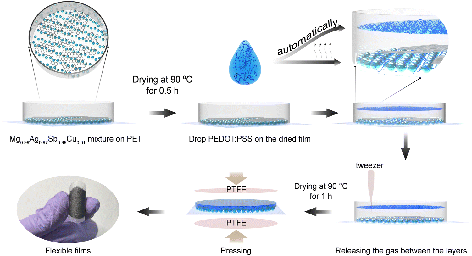 | ||
| Fig. 1 Schematic illustration of the process to synthesize a flexible hybrid film supported by the PTFE membrane. | ||
2.4 Measurement and characterization
The microstructure and elemental distribution were characterized using a Hitachi High-Technologies/Bruker system (FE-SEM, SU8000 + EDS). The crystallographic structure of the as-prepared materials was determined using a simple powder X-ray diffractometer (Rigaku Co., Ltd). The diameter distribution of the MCAS particle sizes was obtained by the scanning electron microscopy (SEM) image analyzed using the Nano Measurer software. The electrical conductivity and Seebeck coefficient values were obtained simultaneously using a commercial instrument (ZEM-3, Advance Riko). The measurement was carried out in a standard four-probe configuration under a helium atmosphere. The Hall measurement was carried out on a ResiTest 8300 Series (Toyo Technica). Raman spectroscopy of hybrid powders was carried out using a Renishaw, micro Raman model inVia Reflex at room temperature under 514 nm laser excitation. X-ray photoelectron spectroscopy (XPS; SigmaProbe, Thermo Fisher Scientific) was performed to identify the composition and the chemical state of surface elements. Spectra were recorded using a spectrometer using a monochromatic Al K-alpha X-ray source (beam energy 1486.6 eV) and a hemispherical electron energy analyzer. Pass energies of 150 eV and 50 eV for survey and core level spectra, respectively, were used. The error bar of TE properties was obtained by repeating the measurements of samples 5 times.3. Results and discussion
The XRD patterns of G, native MCAS powder, MCAS/x wt% G powder and (MCAS)/x wt% G/P hybrid films are compared in Fig. 2a. The XRD patterns of the PTFE substrate, PEDOT:PSS and graphene before and after ball milling (BM) are shown in Fig. S3 (ESI†). The broader peak between dashed lines in Fig. S3a (ESI†) shows the amorphous crystal structure of the pure PEDOT:PSS film on the PTFE substrate. Fig. S3b (ESI†) shows the XRD pattern of graphene before and after BM. Compared to the XRD pattern of the G, the wider full widths at half maximums (FWHM) and the left-shifting of the (002) peak were observed in the pattern of G BM-0.5 hours (see Note I in the ESI†), indicating that the BM process not only reduces the size of graphene nanopalates but also is helpful in increasing its interplanar spacing. In Fig. 3a, all the peaks of native MCAS powder are indexed to the crystal structure of α-MgAgSb, which is consistent with a previous report.36,40,53 Only the diffraction peaks corresponding to the (202), (130), (224), and (141) planes are detected due to the reduced crystallite size after ball milling. As shown in Fig. 2b, the size of the obtained MCAS particles mainly distributes at 1 μm and has an overall size distribution in the range of 0–5 μm. The real chemical composition of the native MCAS powder determined by EDS point-composition analysis is in good agreement with the nominal composition as shown in Fig. S4 (ESI†). In the case of hybrid powder and films, except for the peaks contributed by the strong graphite-2H phase, all peaks are consistent with those of native powder. Besides, the (202) diffraction peak of MCAS disappears in the all hybrid films, indicating that the MCAS grains prefer growing along the (224) orientation. The FWHMs of the (224) characteristic peak of the hybrid films are reduced as compared to the peaks of the corresponding hybrid powder demonstrating the increased crystallite size of MCAS after hot pressing (FWHMs = 0.989° and 0.635° for the MCAS/40 wt% G powder and MCAS/40 wt% G/P film, respectively). In comparison, the peak (224) around 2θ = 40° in the XRD patterns of the hybrid film shifted towards the lower angle for the sample with 10 wt% graphene as compared to the corresponding hybrid powder. The origin of this shift is most likely due to the residual tensile stress of the MCAS powder after the hot pressing process. Also, the narrow FWHMs indicate that the crystallite size of the MCAS is increased after the hot pressing. Moreover, the peak (224) shifted towards a higher angle with increasing graphene content, speculating that the graphene wraps on the surface of MCAS particles and impedes the growth of MCAS under hot pressing. No PEDOT:PSS peak was detected for the hybrid film because of the strong peak intensity of MCAS and G. | ||
| Fig. 2 (a) The XRD patterns of G before and after ball milling, MCAS powder, MACS/x wt% G powder, and MACS/x wt% G/P films (x = 10, 20, 30, 40, and 50). (b) Size distribution of the MACS particles. (c) Raman spectra of G and hybrid MACS/x wt% G powder (x = 10, 20, 30, 40, 50). | ||
 | ||
| Fig. 3 SEM images of (a) native MCAS powder and (b) MCAS powder after hot pressing. (c) Schematic illustration of the interaction between the MCAS particle and graphene. (d) MCAS/40 wt% G film. (e) MCAS/40 wt% G/P film. The ternary film characterized here is constituted by 200 mg mixed powder and 500 μL PEDOT:PSS. | ||
The Raman spectra shown in Fig. 2c further confirm the presence of graphene. Raman spectra for the G before and after ball milling and in the hybrid powder show typical peaks at about 1350, 1580, and 2700 cm−1, which correspond to the D band, G band and 2D band of graphene, respectively. Generally, the structural defects of graphene are related to the intensity ratio of the D band to the G band (ID/IG) in Raman spectroscopy, where a higher ratio corresponds to the higher defect density of the graphene structure. Here, the ID/IG ratio of G before and after BM increases from 0.622 to 0.681 due to the damage of the structure and reduction of the crystallite size of graphene.81,82 However, the ID/IG ratio in the hybrid powder decreases with the wt% increase of graphene, suggesting that the ball milling process brought less damage to the integrity of graphene in the hybrid powder. The I2D/IG ratio is used to estimate the layers of graphene.83 Compared to the as-received G, the I2D/IG intensity ratio decreases from 0.784 to 0.772 after BM-0.5 h, which retains the decreasing trend in the hybrid powders (Table S1, ESI†), indicating the existence of multiple graphene layers.81
The scanning electron microscopy (SEM) images in Fig. 3 show the microstructures of hybrid films formed at different fabrication steps. Fig. 3a shows the microstructure of the native MCAS powder, in which the particles are randomly distributed and connected with each other in a “point to point” fashion. Although the boundary of particles becomes blurry and the porosity is reduced after hot pressing at 100 °C under a pressure of 40 MPa (Fig. 3b), the gaps can still be observed in the hybrid film. Therefore, graphene is intercalated to wrap the particles and form 3D conductive paths for carriers, as schematically illustrated in Fig. 3c, which is partially supported by the SEM-EDS result. As shown in Fig. S5 (ESI†), the C element mapping indicates that the introduced graphene not only wrapped on the MCAS particles but also existed in the gap bridging the particles. In such a structure, the graphene surface acts as a connecting point between the particles, which provides a conductive path that may greatly promote carrier mobility, which will be proved by the Hall measurement result and discussed in the TE properties part. The SEM image of the MCAS/40 wt% graphene film is shown in Fig. 3d, which reveals the formation of a dense film. However, the presence of individual MCAS particles (red circle) and clear interfaces (red arrows) of agglomerated graphene is observed, which can be detrimental to the transport of carriers and may lead to a poor σ.58 In contrast, the MCAS/G/P film shows the homogenous distribution of graphene, and no clear graphene interfaces are observed, which is ascribed to the π–π interaction between graphene and PEDOT:PSS, which is further proved by C 1s spectra in Raman measurement.84 The stacked graphene nanoplates in the hybrid binary film interact with each other or with particles through the van der Waals force.77 However, after drop-casting PEDOT:PSS, the greater π–π interaction between graphene and PEDOT:PSS makes the graphene nanoplates redistribute more homogeneously in the matrix (Fig. 3e).58,84 The elemental distribution and homogeneity of the pure powder and ternary hybrid film are further investigated by EDS (Fig. S6, ESI†). The results show that all the elements are homogeneously distributed throughout the sample and graphene homogenously wraps the particles.
Fig. 4a shows the XPS survey spectra of G before and after BM, MCAS and MCAS/40 wt%G hybrid powder as well as MCAS/40 wt%G/P films with different MCAS/G mass loadings (79.1 wt% and 88.3 wt%, respectively). The spectra of G before and after BM keep consistent the binding energies (BEs) of C 1s and O 1s, suggesting that the ball milling process does not influence the element composition of graphene. C 1s was detected in all hybrid samples indicating the inclusion of graphene in all hybrid samples. Note that it is speculated that O 1s is contributed by the O2 absorbed on the surface of the samples because the XRD results (Fig. 2) indicate the graphite 2H phase of both graphene before and after ball milling samples.85,86 The spectrum of the native MCAS powder confirms the presence of Mg, Cu, Ag, and Sb of native powder. In contrast, the S 2p belonging to PEDOT:PSS was only detected in the MCAS/G/P hybrid films.
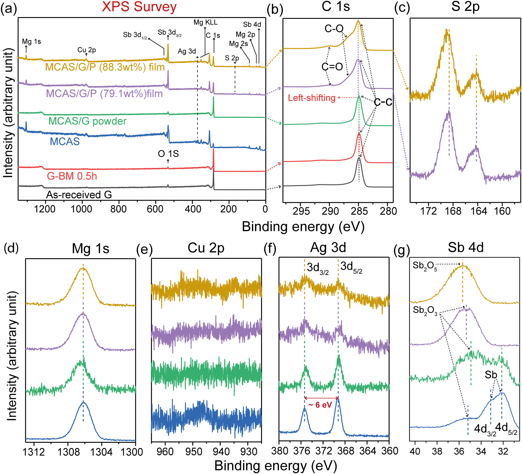 | ||
| Fig. 4 (a) XPS survey spectra of pure G, G BM-0.5h, MCAS powder, MCAS/G powder, the MCAS/G/P film at 79.1 wt% and the MCAS/G/P film at 88.3 wt%. All the spectra have been staggered vertically for the clarity of presentation. High resolution (b) C 1s, (c) S 2p, (d) Mg 1s, (e) Cu 2p, (f) Ag 3d, and (g) Sb 4d spectra of MCAS and MCAS/40 wt%G hybrid powder as well as the MCAS/G/P films. | ||
Fig. 4(b and c) show the C 1s and S 2p core level spectra of the samples. In the C 1s spectra, except the C–C group (at ∼284.5 eV) belonging to graphene, it is observed that the characteristic C–O (∼285.9 eV) and C![[double bond, length as m-dash]](https://www.rsc.org/images/entities/char_e001.gif) O (∼287.3 eV) groups were ascribed to PEDOT:PSS.87,88 In addition, the strong π–π interaction between graphene and PEDOT:PSS contributes to the slightly left-shifting of the C–C peak in the hybrid films.89 The similar peak ratio in the S 2p spectra suggests that PEDOT:PSS is stable in the process of film fabrication.
O (∼287.3 eV) groups were ascribed to PEDOT:PSS.87,88 In addition, the strong π–π interaction between graphene and PEDOT:PSS contributes to the slightly left-shifting of the C–C peak in the hybrid films.89 The similar peak ratio in the S 2p spectra suggests that PEDOT:PSS is stable in the process of film fabrication.
The Mg 1s, Cu 2p, Ag 3d, and Sb 4d core level spectra are shown in Fig. 4(d and g). No appreciable change in the BE and line shape of core levels were observed except the Sb 4d spectra. The peak position at ∼1306.2 eV in the Mg 1s spectra implies the Mg2+ oxidation state (1305.0 eV) on the surface of the MCAS alloy. In contrast, the detected peaks for Cu were too weak to identify the BE position (Fig. 4e). In the spectra of Ag 3d, the two peaks at 369.4 eV and 375.4 eV correspond to Ag 3d3/2 (368.3 eV) and Ag 3d5/2 (374.3 eV), and the value of spin–orbit splitting is calculated to be ∼6 eV, which implies that the Ag ion is in the +1 oxidation state. In comparison, the signal intensity of Ag 3d gradually decreases from the native powder to hybrid powder to hybrid films, proving that the Ag signal of MCAS was weakened by the layers of graphene in the hybrid powder as well as graphene with PEDOT:PSS in the hybrid films, which is also in accordance with its atomic distribution (Table S2, ESI†). From the spectra of Sb 4d, it is known that the part of Sb (pure Sb 4d5/2 at 32.1 eV and 4d3/2 at 33.3 eV) is the oxidized state (4d5/2 at 34.56 eV for Sb2O3 and 4d3/2 at 35.74 eV for Sb2O5) on the surface of the MCAS powder. Compared with the MCAS powder, the oxidation of Sb is serious on the surface of the hybrid powder even in the hybrid films. Moreover, the BE positions of all the peaks measured in this study slightly move to the higher BE position compared to the corresponding standard position (all BE positions mentioned in brackets were obtained from the Handbook90), indicating that the element states of MCAS are contributed by both oxidation and interaction among elements. Nevertheless, combining the XRD results (Fig. 2a), it is concluded that the oxidation amount of samples is negligible because no impurity phase was detected by XRD.
To optimize the graphene content in the hybrid film, the electrical properties σ, S, and PF of hybrid films at room temperature as a function of graphene content are shown in Fig. 5a. The σ of the hybrid film increases slowly with the graphene content up to 30 wt%, then it increases abruptly at 40 wt% and decreases at 50 wt% (Fig. 5a). The σ value increases from 12 S cm−1 for the 0 wt% hybrid film to a maximum of 933 S cm−1 for the 40 wt% hybrid film. The optimization of graphene content leads to an increase in σ(σ = neμ), which is mainly attributed to either the increase in the concentration (n) or the mobility (μ) of the hybrid films. Fig. 5b shows the n and μ of the hybrid films measured at room temperature. As the graphene content varies from 0 wt% to 50 wt%, the n value increases from ∼5 × 1017 cm−3 (0 wt%) to ∼4.5 × 1020 cm−3 (50 wt%), which is most likely a result of graphene that introduces additional carriers into the matrix.91–93 Moreover, the μ value increases from ∼1 cm2 V−1 s−1 (0 wt%) to ∼5 cm2 V−1 s−1 (40 wt%) because of the reduced void volume fraction between matrix particles by the addition of graphene content. However, the decrease of both μ and σ for the 50 wt% graphene sample is due to the segregation of graphene nanoplates at the particle boundaries, creating new microstructural interfaces and providing extra boundaries.58,94
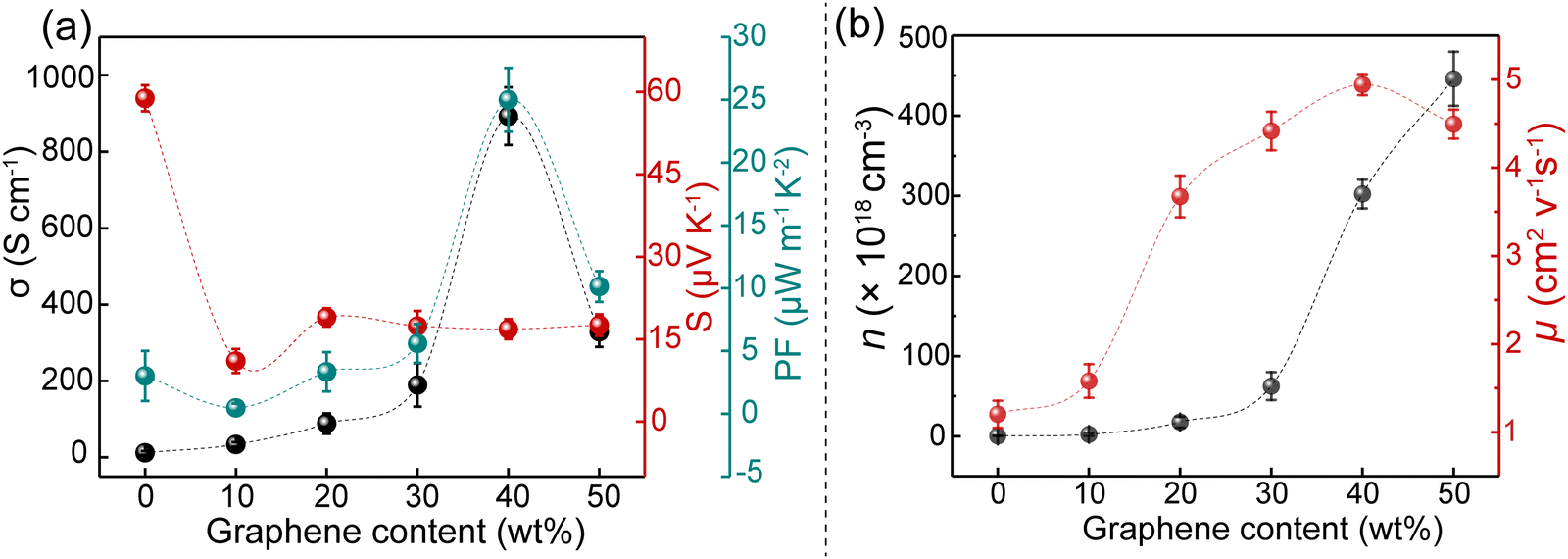 | ||
| Fig. 5 TE properties of the hybrid film as a function of graphene content by hybrid 200 mg of mixed powder with 500 μL of PEDOT:PSS: (a) σ, S, and PF; (b) carrier concentration (n) and mobility (μ). | ||
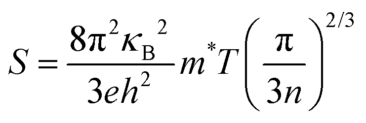
The positive Seebeck coefficients at room temperature for all the hybrid films show that the majority of carriers are holes (Fig. 5a). The S decreases significantly with an increase of graphene content up to 10 wt%, whereas it shows similar S values with a further increase of graphene content. The S follows the n−2/3 dependence according to Mott's formula,95i.e., expressed as
We have successfully demonstrated the preparation of a crack-free hybrid film with good TE properties. However, mechanical flexibility is essential for the social implementation of hybrid film TE devices. Therefore, the influence of the hybrid mass fraction on both the TE properties and mechanical flexibility of the ternary hybrid film is further investigated.
Fig. 6 shows the σ, S, and PF of hybrid films as a function of the MCAS/40 wt% G mass fraction. The σ increases with the mass fraction, whereas S is almost invariant, leading to a high PF with a similar trend to σ. The increase of σ from 258 S cm−1 (79.1 wt%) to 922 S cm−1 (93.8 wt%) is mainly due to the increase of μ. Fig. 6b shows similar n values whereas μ increases with varying mass fractions. The μ increases from ∼1 cm2 V−1 s−1 (79.1 wt%) to ∼3 cm2 V−1 s−1 (93.8 wt%), whereas the n value is ∼0.5 × 1020 cm−3 for all the hybrid films. As a combined effect of high σ and moderate S, a maximum PF (S2σ) of 31 μW m−1 K−2 is obtained for the 93.8 wt% mass fraction hybrid film.
 | ||
| Fig. 6 (a) σ, S, and PF of the hybrid films as a function of the MCAS/G mass fraction. (b) The evolution of carrier concentration and mobility with the varying mass fraction. (c) The variation of σ and (d) S of the hybrid films loading with different MCAS/G mass fractions as a function of bending times. | ||
Although the mobility shows the unsaturated trend in the mass fraction range studied, the mechanical bending tests confirm that the 88.3 wt% mass fraction is optimum to obtain a hybrid film with the required flexibility. Fig. 6c and d show σ and S as a function of bending times for 79.1 wt% and 88.3 wt% mass fraction. The bending tests are performed by applying the hybrid film around a glass rod with a diameter of 12.6 mm. Within 1000 bending times, the σ of both films (79.1 wt% and 88.3 wt%) shows a similar evolving trend and a slight decrease (retaining 70.8% at 79.1 wt% and 77% at 88.3 wt% after 1000 bending times). In particular, the film at an 88.3 wt% mass fraction shows a relative obvious decrease trend from 900 to 1000 bending times compared to that of the film at 79.1 wt%, indicating that the flexibility of the hybrid films at a higher mass fraction is easily sacrificed with the increase of bending times. As shown in Fig. S7(a and b) (ESI†), the thickness of the hybrid film increased with the increase of hybrid powder content. Consequently, with an increase in the bending tests, the hybrid film with higher mass loading (88.3 wt%) demonstrates a bigger crack (Fig. S7c and d, ESI†), leading to a more obvious decrease of σ at higher bending times. In contrast, the S of the film at 88.3 wt% is invariant as the function of bending time in comparison to the S at 79.1 wt%. This result shows a significant variation and is possibly caused by the hybrid ratio of three components (inorganic TE material, PEDOT:PSS, and graphene). The hybrid film is expected to be detrimental for TE properties at different areas and bending times with a lower mass fraction; therefore, the resultant S is obtained by their respective S ratio in the hybrid film. However, with the increase of the mass fraction, the S of an inorganic material part may become dominant, so that the hybrid film at 88.3 wt% shows a similar S value with increasing bending times. The σ and S evolution as a function of bending times of the hybrid films at 91.9 wt% and 93.8 wt% are not obtained because the films are seriously damaged during the first 100 times bending tests. The TE properties and flexibility of the hybrid film at 79.1 wt% are compared with the reported data (Table S3, ESI†). The electrical conductivity of the hybrid film in the present work is comparable with reported data; however, it is less flexible in comparison to the hybrid films fabricated using nanowire based inorganic components,97–100 which mainly resulted from the “point to point” connection way of inorganic particles.
4. Conclusions
We successfully demonstrated a facile method for the fabrication of a crack-free p-type flexible Mg0.99Cu0.01Ag0.97Sb0.99/graphene/PEDOT:PSS (MCAS/G/P) hybrid film. The electrical properties of the TE films were optimized by varying the graphene content. The TE film with the optimized graphene content (40 wt%) showed a maximum electrical conductivity of 933 S cm−1 and a power factor of 25 μW m−1 K−2 at room temperature. The enhanced PF of the hybrid film for 40 wt% graphene results from the optimized conductive path in MCAS, which not only enhanced the σ but also endowed the hybrid film with excellent flexibility. Moreover, the mechanical bending tests confirmed that the σ and S of the hybrid film were retained more than 71% after 1000 bending times. This result indicates that there is still room to improve the flexibility and TE properties of the MCAS/graphene/PEDOT:PSS hybrid film. However, the present work may facilitate to develop novel high-performance thermoelectric materials with flexibility for harvesting the waste heat.Author contributions
Yanan Wang: data curation, formal analysis, investigation, methodology, and writing – original draft. Raju Chetty: writing – review and editing and formal analysis. Zihangliu, Longquan Wang, Takeo Ohsawa and Weihong Gao: writing – review and editing and formal analysis. Takao Mori: project administration, supervision, and writing – review and editing and validation.Conflicts of interest
There are no conflicts to declare.Acknowledgements
This work was supported by the JST Mirai Program Grant JPMJMI19A1. Y. W gratefully acknowledges financial support from the China Scholarship Council (CSC).References
- L. Li, W. D. Liu, Q. Liu and Z. G. Chen, Adv. Funct. Mater., 2022, 32, 2200548 CrossRef CAS.
- L. E. Bell, Science, 2008, 321, 1457–1461 CrossRef CAS PubMed.
- T. Mori and S. Priya, MRS Bull., 2018, 43, 176–180 CrossRef.
- R. A. Kishore and S. Priya, Materials, 2018, 11, 1433 CrossRef PubMed.
- L. Yang, Z.-G. Chen, M. S. Dargusch and J. Zou, Adv. Energy Mater., 2018, 8, 1701797 CrossRef.
- S. Hooshmand Zaferani, M. Jafarian, D. Vashaee and R. Ghomashchi, Energies, 2021, 14, 5646 CrossRef CAS.
- I. Petsagkourakisa, K. Tybrandta, X. Crispin, I. Ohkubo, N. Satoh and T. Mori, Sci. Technol. Adv. Mater., 2018, 19, 836–862 CrossRef PubMed.
- D. Qu, X. Li, H. Wang and G. Chen, Adv. Sci., 2019, 6, 1900584 CrossRef PubMed.
- N. Nandihalli, C.-J. Liu and T. Mori, Nano Energy, 2020, 78, 105186 CrossRef CAS.
- Q. Xu, B. Deng, L. Zhang, S. Lin, Z. Han, Q. Zhou, J. Li, Y. Zhu, F. Jiang, Q. Li, P. Zhang, X. Zhang, G. Chen and W. Liu, Cell Rep. Phys. Sci., 2022, 3, 100780 CrossRef CAS.
- J. He and T. M. Tritt, Science, 2017, 357, 1369 CAS.
- T. Mori, Small, 2017, 13, 1702013 CrossRef PubMed.
- X. Zhou, Y. Yan, X. Lu, H. Zhu, X. Han, G. Chen and Z. Ren, Mater. Today, 2018, 21, 974–988 CrossRef CAS.
- Y. Xiao and L.-D. Zhao, Science, 2020, 367, 1196–1197 CrossRef CAS PubMed.
- Z. Liu and T. Mori, inSystem-Materials Nanoarchitectonics, ed. Y. Wakayama and K. Ariga, 2022, pp. 199–231 Search PubMed.
- B. Poudel, Q. Hao, Y. Ma, Y. Lan, A. Minnich, B. Yu, X. Yan, D. Wang, A. Muto, D. Vashaee, X. Chen, J. Liu, M. S. Dresselhaus, G. Chen and Z. Ren, Science, 2008, 320, 634–638 CrossRef CAS PubMed.
- K. Biswas, J. He, I. D. Blum, C. I. Wu, T. P. Hogan, D. N. Seidman, V. P. Dravid and M. G. Kanatzidis, Nature, 2012, 489, 414–418 CrossRef CAS PubMed.
- C. Fu, S. Bai, Y. Liu, Y. Tang, L. Chen, X. Zhao and T. Zhu, Nat. Commun., 2015, 6, 8144 CrossRef PubMed.
- L.-D. Zhao, G. Tan, S. Hao, J. He, Y. Pei, H. Chi, H. Wang, S. Gong, H. Xu, V. P. Dravid, C. Uher, G. J. S. Snyder, C. Wolverton and M. G. Kanatzidis, Science, 2016, 351, 141–144 CrossRef CAS PubMed.
- A. U. Khan, K. Kobayashi, D.-M. Tang, Y. Yamauchi, K. Hasegawa, M. Mitome, Y. Xue, B. Jiang, K. Tsuchiya, D. Golberg, Y. Bando and T. Mori, Nano Energy, 2017, 31, 152–159 CrossRef CAS.
- H. Zhu, J. Mao, Z. Feng, J. Sun, Q. Zhu, Z. Liu, D. J. Singh, Y. Wang and Z. Ren, Sci. Adv., 2019, 5, eaav5813 CrossRef PubMed.
- J. Yu, Y. Xing, C. Hu, Z. Huang, Q. Qiu, C. Wang, K. Xia, Z. Wang, S. Bai, X. Zhao, L. Chen and T. Zhu, Adv. Energy Mater., 2020, 10, 2000888 CrossRef CAS.
- X. Hu, P. Jood, M. Ohta, M. Kunii, K. Nagase, H. Nishiate, M. G. Kanatzidis and A. Yamamoto, Energy Environ. Sci., 2016, 9, 517–529 RSC.
- P. Jood, M. Ohta, A. Yamamoto and M. G. Kanatzidis, Joule, 2018, 2, 1339–1355 CrossRef CAS.
- J. R. Salvador, J. Y. Cho, Z. Ye, J. E. Moczygemba, A. J. Thompson, J. W. Sharp, J. D. Koenig, R. Maloney, T. Thompson, J. Sakamoto, H. Wang and A. A. Wereszczak, Phys. Chem. Chem. Phys., 2014, 16, 12510–12520 RSC.
- S. El Oualid, I. Kogut, M. Benyahia, E. Geczi, U. Kruck, F. Kosior, P. Masschelein, C. Candolfi, A. Dauscher, J. D. Koenig, A. Jacquot, T. Caillat, E. Alleno and B. Lenoir, Adv. Energy Mater., 2021, 11, 2100580 CrossRef CAS.
- A. Nozariasbmarz, U. Saparamadu, W. Li, H. B. Kang, C. Dettor, H. Zhu, B. Poudel and S. Priya, J. Power Sources, 2021, 493, 229695 CrossRef CAS.
- Y. Du, J. Xu, B. Paul and P. Eklund, Appl. Mater. Today, 2018, 12, 366–388 CrossRef.
- Q. Jiang, J. Yang, P. Hing and H. Ye, Adv. Mater., 2020, 1, 1038–1054 RSC.
- X. Wang, J. Cheng, L. Yin, Z. Zhang, X. Wang, J. Sui, X. Liu, J. Mao, F. Cao and Q. Zhang, Adv. Funct. Mater., 2022, 32, 2200307 CrossRef CAS.
- D. W. Ao, W. D. Liu, Y. X. Chen, M. Wei, B. Jabar, F. Li, X. L. Shi, Z. H. Zheng, G. X. Liang, X. H. Zhang, P. Fan and Z. G. Chen, Adv. Sci., 2022, 9, e2103547 CrossRef PubMed.
- O. Norimasa, T. Chiba, M. Hase, T. Komori and M. Takashiri, J. Alloys Compd., 2022, 898, 162889 CrossRef CAS.
- Y. Lei, R. Qi, M. Chen, H. Chen, C. Xing, F. Sui, L. Gu, W. He, Y. Zhang, T. Baba, T. Baba, H. Lin, T. Mori, K. Koumoto, Y. Lin and Z. Zheng, Adv. Mater., 2021, 34, 2104786 CrossRef PubMed.
- J. Liang, T. Wang, P. Qiu, S. Yang, C. Ming, H. Chen, Q. Song, K. Zhao, T.-R. Wei, D. Ren, Y.-Y. Sun, X. Shi, J. He and L. Chen, Energy Environ. Sci., 2019, 12, 2983–2990 RSC.
- X. Li, Y. Lu, K. Cai, M. Gao, Y. Li, Z. Wang, M. Wu, P. Wei, W. Zhao, Y. Du and S. Shen, Chem. Eng. J., 2022, 434, 134739 CrossRef CAS.
- M. J. Kirkham, A. M. dos Santos, C. J. Rawn, E. Lara-Curzio, J. W. Sharp and A. J. Thompson, Phys. Rev. B: Condens. Matter Mater. Phys., 2012, 85, 144120 CrossRef.
- H. Zhao, J. Sui, Z. Tang, Y. Lan, Q. Jie, D. Kraemer, K. McEnaney, A. Guloy, G. Chen and Z. Ren, Nano Energy, 2014, 7, 97–103 CrossRef CAS.
- D. Kraemer, J. Sui, K. McEnaney, H. Zhao, Q. Jie, Z. F. Ren and G. Chen, Energy Environ. Sci., 2015, 8, 1299–1308 RSC.
- J. Shuai, H. S. Kim, Y. Lan, S. Chen, Y. Liu, H. Zhao, J. Sui and Z. Ren, Nano Energy, 2015, 11, 640–646 CrossRef CAS.
- J. Sui, J. Shuai, Y. Lan, Y. Liu, R. He, D. Wang, Q. Jie and Z. Ren, Acta Mater., 2015, 87, 266–272 CrossRef CAS.
- P. Ying, X. Liu, C. Fu, X. Yue, H. Xie, X. Zhao, W. Zhang and T. Zhu, Chem. Mater., 2015, 27, 909–913 CrossRef CAS.
- Z. Liu, H. Geng, J. Mao, J. Shuai, R. He, C. Wang, W. Cai, J. Sui and Z. Ren, J. Mater. Chem. A, 2016, 4, 16834–16840 RSC.
- Z. Liu, J. Shuai, J. Mao, Y. Wang, Z. Wang, W. Cai, J. Sui and Z. Ren, Acta Mater., 2016, 102, 17–23 CrossRef CAS.
- Z. Liu, Y. Wang, J. Mao, H. Geng, J. Shuai, Y. Wang, R. He, W. Cai, J. Sui and Z. Ren, Adv. Energy Mater., 2016, 6, 1502269 CrossRef.
- Z. Liu, W. Gao, X. Meng, X. Li, J. Mao, Y. Wang, J. Shuai, W. Cai, Z. Ren and J. Sui, Scr. Mater., 2017, 127, 72–75 CrossRef CAS.
- Z. Liu, Y. Wang, W. Gao, J. Mao, H. Geng, J. Shuai, W. Cai, J. Sui and Z. Ren, Nano Energy, 2017, 31, 194–200 CrossRef CAS.
- Z. Liu, Y. Zhang, J. Mao, W. Gao, Y. Wang, J. Shuai, W. Cai, J. Sui and Z. Ren, Acta Mater., 2017, 128, 227–234 CrossRef CAS.
- D. Li, H. Zhao, S. Li, B. Wei, J. Shuai, C. Shi, X. Xi, P. Sun, S. Meng, L. Gu, Z. Ren and X. Chen, Adv. Funct. Mater., 2015, 25, 6478–6488 CrossRef CAS.
- Naihua Miao, Jian Zhou, B. Sa, Bin Xu and Z. Sun, Appl. Phys. Lett., 2016, 108, 213902 CrossRef.
- C. Y. Sheng, H. J. Liu, D. D. Fan, L. Cheng, J. Zhang, J. Wei, J. H. Liang, P. H. Jiang and J. Shi, J. Appl. Phys., 2016, 119, 195101 CrossRef.
- J.-F. Wang, X.-N. Fu, X.-D. Zhang, J.-T. Wang, X.-D. Li and Z.-Y. Jiang, Chin. Phys. B, 2016, 25, 086302 CrossRef.
- P. Ying, X. Li, Y. Wang, J. Yang, C. Fu, W. Zhang, X. Zhao and T. Zhu, Adv. Funct. Mater., 2017, 27, 1604145 CrossRef.
- Z. Liu, N. Sato, W. Gao, K. Yubuta, N. Kawamoto, M. Mitome, K. Kurashima, Y. Owada, K. Nagase, C.-H. Lee, J. Yi, K. Tsuchiya and T. Mori, Joule, 2021, 5, 1196–1208 CrossRef CAS.
- P. Ying, R. He, J. Mao, Q. Zhang, H. Reith, J. Sui, Z. Ren, K. Nielsch and G. Schierning, Nat. Commun., 2021, 12, 1121 CrossRef CAS.
- Z. Liu, W. Gao, H. Oshima, K. Nagase, C. H. Lee and T. Mori, Nat. Commun., 2022, 13, 1120 CrossRef CAS.
- G. Prunet, F. Pawula, G. Fleury, E. Cloutet, A. J. Robinson, G. Hadziioannou and A. Pakdel, Mater. Today Phys., 2021, 18, 100402 CrossRef CAS.
- B. Ni, C. Fu, S. Pan, L. He, Z. Lin and J. Peng, Chem. Mater., 2022, 34, 847–853 CrossRef CAS.
- Y. Wang, H. Pang, Q. Guo, N. Tsujii, T. Baba, T. Baba and T. Mori, ACS Appl. Mater. Interfaces, 2021, 13, 51245–51254 CrossRef CAS PubMed.
- D. Yoo, J. Kim and J. H. Kim, Nano Res., 2014, 7, 717–730 CrossRef CAS.
- M. N. Gueye, A. Carella, J. Faure-Vincent, R. Demadrille and J.-P. Simonato, Prog. Mater. Sci., 2020, 108, 100616 CrossRef CAS.
- W. Li, H. Wang, X. Hu, W. Cai, C. Zhang, M. Wang and Z. Zang, Sol. RRL, 2021, 5, 2000573 CrossRef CAS.
- M. Wang, W. Li, H. Wang, K. Yang, X. Hu, K. Sun, S. Lu and Z. Zang, Adv. Electron. Mater., 2020, 6, 2000604 CrossRef CAS.
- M. Wang, H. Wang, W. Li, X. Hu, K. Sun and Z. Zang, J. Mater. Chem. A, 2019, 7, 26421–26428 RSC.
- F. Huang, H. Wu and Y. Cao, Chem. Soc. Rev., 2010, 39, 2500–2521 RSC.
- M. N. Gueye, A. Carella, R. Demadrille and J.-P. Simonato, ACS Appl. Mater. Interfaces, 2017, 9, 27250–27256 CrossRef CAS PubMed.
- B. D. Paulsen, K. Tybrandt, E. Stavrinidou and J. Rivnay, Nat. Mater., 2020, 19, 13–26 CrossRef CAS.
- M. Solazzo, K. Krukiewicz, A. Zhussupbekova, K. Fleischer, M. J. Biggs and M. G. Monaghan, J. Mater. Chem. B, 2019, 7, 4811–4820 RSC.
- Z. Fan and J. Ouyang, Adv. Electron. Mater., 2019, 5, 1800769 CrossRef CAS.
- X. Hu, K. Zhang, J. Zhang, S. Wang and Y. Qiu, ACS Appl. Energy Mater., 2018, 1, 4883–4890 CrossRef CAS.
- D. Ni, H. Song, Y. Chen and K. Cai, J. Materiomics, 2020, 6, 364–370 CrossRef.
- Y. Du, X. Liu, J. Xu and S. Z. Shen, Mater. Chem. Front., 2019, 3, 1328–1334 RSC.
- B. Zhang, J. Sun, H. E. Katz, F. Fang and R. L. Opila, ACS Appl. Mater. Interfaces, 2010, 2, 3170–3178 CrossRef CAS.
- Y. Wang, M. Hong, W.-D. Liu, X.-L. Shi, S.-D. Xu, Q. Sun, H. Gao, S. Lu, J. Zou and Z.-G. Chen, Chem. Eng. J., 2020, 397, 125360 CrossRef CAS.
- F. Schedin, A. K. Geim, S. V. Morozov, E. W. Hill, P. Blake, M. I. Katsnelson and K. S. Novoselov, Nat. Mater., 2007, 6, 652–655 CrossRef CAS PubMed.
- C. Lee, X. W. Wei, J. W. Kysar and J. Hone, Science, 2008, 321, 385–388 CrossRef CAS PubMed.
- A. H. Castro Neto, F. Guinea, N. M. R. Peres, K. S. Novoselov and A. K. Geim, Rev. Mod. Phys., 2009, 81, 109–162 CrossRef CAS.
- Y. Liu, N. O. Weiss, X. Duan, H.-C. Cheng, Y. Huang and X. Duan, Nat. Rev. Mater., 2016, 1, 1–17 Search PubMed.
- M. Alsalama, H. Hamoudi and K. M. Youssef, J. Alloys Compd., 2021, 159584, DOI:10.1016/j.jallcom.2021.159584.
- K. Ahmad, C. Wan, M. A. Al-Eshaikh and A. N. Kadachi, Appl. Surf. Sci., 2019, 474, 2–8 CrossRef CAS.
- P.-a Zong, X. Chen, Y. Zhu, Z. Liu, Y. Zeng and L. Chen, J. Mater. Chem. A, 2015, 3, 8643–8649 RSC.
- M. Li, H. Gao, J. Liang, S. Gu, W. You, D. Shu, J. Wang and B. Sun, Mater. Charact., 2018, 140, 172–178 CrossRef CAS.
- D. Poirier, R. Gauvin and R. A. L. Drew, Composites, Part A, 2009, 40, 1482–1489 CrossRef.
- F. Chen, J. Ying, Y. Wang, S. Du, Z. Liu and Q. Huang, Carbon, 2016, 96, 836–842 CrossRef CAS.
- E. Bilotti, O. Fenwick, B. C. Schroeder, M. Baxendale, P. Taroni-Junior, T. Degousée and Z. Liu, Compr. Compos. Mater. II, 2018, 6, 408–430 CAS.
- Z.-J. Fan, W. Kai, J. Yan, T. Wei, L.-J. Zhi, J. Feng, Y.-m Ren, L.-P. Song and F. Wei, ACS Nano, 2011, 5, 191–198 CrossRef CAS PubMed.
- H. M. A. Hassan, V. Abdelsayed, A. E. R. S. Khder, K. M. AbouZeid, J. Terner, M. S. El-Shall, S. I. Al-Resayes and A. A. El-Azhary, J. Mater. Chem., 2009, 19, 3832 RSC.
- G. H. Kim, D. H. Hwang and S. I. Woo, Phys. Chem. Chem. Phys., 2012, 14, 3530–3536 RSC.
- D. Yoo, J. Kim and J. H. Kim, Nano Res., 2014, 7, 717–730 CrossRef CAS.
- Q. Su, S. Pang, V. Alijani, C. Li, X. Feng and K. Müllen, Adv. Mater., 2009, 21, 3191–3195 CrossRef CAS.
- J. Chastain and R. C. King Jr, PerkinElmer Corp., 1992, 40, 221 Search PubMed.
- F. Ghahari, H. Y. Xie, T. Taniguchi, K. Watanabe, M. S. Foster and P. Kim, Phys. Rev. Lett., 2016, 116, 136802 CrossRef PubMed.
- P. Wei, W. Bao, Y. Pu, C. N. Lau and J. Shi, Phys. Rev. Lett., 2009, 102, 166808 CrossRef PubMed.
- Y. M. Zuev, W. Chang and P. Kim, Phys. Rev. Lett., 2009, 102, 096807 CrossRef PubMed.
- S. H. Zaferani, R. Ghomashchi and D. Vashaee, ACS Appl. Energy Mater., 2021, 4, 3573–3583 CrossRef CAS.
- G. J. Snyder and E. S. Toberer, Materials for Sustainable Energy, World Scientific Publishing Co. Pte. Ltd, Singapore, 2010, pp. 101–110 Search PubMed.
- J. Choi, J. Y. Lee, S.-S. Lee, C. R. Park and H. Kim, Adv. Energy Mater., 2016, 6, 1502181 CrossRef.
- Y. Lu, Y. Qiu, K. Cai, X. Li, M. Gao, C. Jiang and J. He, Mater. Today Phys., 2020, 14, 100223 CrossRef.
- Y. Lu, Y. Qiu, Q. Jiang, K. Cai, Y. Du, H. Song, M. Gao, C. Huang, J. He and D. Hu, ACS Appl. Mater. Interfaces, 2018, 10, 42310–42319 CrossRef CAS PubMed.
- Q. Meng, Y. Qiu, K. Cai, Y. Ding, M. Wang, H. Pu, Q. Yao, L. Chen and J. He, ACS Appl. Mater. Interfaces, 2019, 11, 33254–33262 CrossRef CAS PubMed.
- Y. Lu, Y. Ding, Y. Qiu, K. Cai, Q. Yao, H. Song, L. Tong, J. He and L. Chen, ACS Appl. Mater. Interfaces, 2019, 11, 12819–12829 CrossRef CAS PubMed.
Footnote |
| † Electronic supplementary information (ESI) available: The optical image of the cracked film, the optical pictures of the fabrication process of the hybrid film, XRD patterns, SEM-EDS images, tables of Raman and XPS data and the comparison of the TE properties. See DOI: https://doi.org/10.1039/d2tc02176e |
| This journal is © The Royal Society of Chemistry 2022 |