
 Open Access Article
 This Open Access Article is licensed under a
 Creative Commons Attribution 3.0 Unported Licence
Amino-acid-directed formation of quasi-zero-dimensional perovskites for high-purity blue and red luminescence†
Baisheng
Zhu
 a,
Tian
Wang
a and
Zhi-Kuang
Tan
*ab
a,
Tian
Wang
a and
Zhi-Kuang
Tan
*ab
aDepartment of Chemistry, National University of Singapore, 3 Science Drive 3, 117543, Singapore. E-mail: chmtanz@nus.edu.sg
bSolar Energy Research Institute of Singapore, National University of Singapore, 7 Engineering Drive 1, 117574, Singapore
First published on 12th July 2022
Abstract
Spectral tuning in lead halide perovskite semiconductors is generally achieved by mixing halide compositions or by quantum confinement effects. However, mixed-halide perovskites exhibit undesirable phase separation during optical and electrical excitations, leading to spectral instability. Quantum confinement in pure-halide perovskite nanocrystals circumvents this problem, but requires synthetic protocols that involve high loading of long-chain insulating ligands. Here, we report a unique formation of quantum-confined perovskite through a one-step solution-casting process. This is achieved by the implementation of a short-chain 3-ammonium propionic acid (3-APA+) additive in the precursor solution, which directs quantum-confined nano-domains to assemble in situ during film formation. The bidentate amino and carboxylate functional groups of 3-APA+, at an operational three-carbon spacing, coordinate effectively to adjacent halide and cesium surface atoms, and thus stabilizes the formation of quasi-zero dimensional nano-domains within an otherwise continuous thin film (i.e. embedded quantum dots within bulk film). This process allows precise spectral tuning in both pure-bromide and pure-iodide perovskite thin films to give high-purity blue and red luminescence, respectively. The resulting electroluminescent diodes exhibit remarkable spectral stability at 468 nm and 638 nm, which could find functional applications in trichromatic electronic color displays.
Introduction
Metal halide perovskites are promising semiconductors for light-emitting devices due to their facile processing, defect tolerance, tunable emission, narrow emission linewidths, and exceptional photoluminescence quantum yields (PLQY).1–6 To date, green and near-infrared perovskite light-emitting diodes (LEDs) have achieved impressive external quantum efficiencies (EQEs) exceeding 20%.7–13 To attain a full color gamut in a display, the three primary colors are required, including red, green, and blue.14 However, blue perovskite LEDs still lag in their efficiency and stability, especially in the deep blue region (455–475 nm).15,16 Red perovskite LEDs also possess undesirable spectral stability.3Perovskites may be tuned to emit in blue and red via two approaches, i.e. by chemical composition and quantum confinement.9,17–19 So far, modulating the halide anions is an easier and more straightforward method to tune the bandgap towards the desired emission wavelength. However, mixed-halide perovskites exhibit intrinsic phase instabilities due to anion phase-segregation, especially under electrical bias.3,20,21 As an alternative strategy, quantum confinement effects may be employed for bandgap engineering, such as using mixed-dimensional perovskites or colloidal perovskite nanocrystals. Quantum-well (QW) structures can be generated via reduced-dimensional (quasi-2D and quantum dots) perovskites with large organic cations or ligands.4,17 For instance, the emission of CsPbBr3 can be tuned from green to deep blue in quantum dots (QDs) (<∼7 nm Bohr radius),5 nanowires,22 nanoplatelets,23 and nanostrips.24 Excess insulating ligands could, however, lead to problematic charge injection and transport in PeLEDs.25
In this work, we demonstrate the preparation of quantum-confined perovskites through a convenient one-step solution-casting process. This is enabled by the addition of a short-chain 3-ammonium propionic acid (3-APA+) chelating agent into the perovskite precursor solution. The –COOH and –NH3+ groups from 3-APA+ cations coordinate with cesium-halide-rich surfaces and restrict crystal growth, thus giving rise to the in situ formation nano-domains during the film casting process. The emission of (3-ammonium propionic acid bromide) 3-APAB treated CsPbBr3 films can be tuned between cyan (500 nm) and deep blue (445 nm), with corresponding PLQY ranging from 5.4% to 40.1%. In addition, 3-APA+ cations can also enable the preparation of quantum-confined CsPbI3, emitting in the range of 621 nm to 690 nm.
Experimental section
Materials
Lead bromide (PbBr2, Sigma-Aldrich, 99.999%), lead iodide (PbI2, Sigma-Aldrich, 99.999%), cesium bromide (CsBr, Sigma-Aldrich, 99.999%), cesium iodide (CsI, Sigma-Aldrich, 99.999%), 3-Ammonium propionic acid bromide (3-APAB, Greatcell solar, >98%), 3-Ammonium propionic acid iodide (3-APAI, Greatcell solar, >98%), n-propylammonium bromide (PAB, Sigma-Aldrich, >98%), Propanoic acid (PA, Sigma-Aldrich, 99%), 4-Ammonium butyric acid bromide (ABAB, Greatcell solar, >98%), 5-Ammonium valeric acid bromide (AVAB, Greatcell solar, >99%), Dimethyl sulfoxide (DMSO) (anhydrous, Sigma-Aldrich, 99.9%), nickel nitrate hexahydrate (Ni(NO3)2·6H2O, Sigma-Aldrich, 99.99%), ethylene diamine (C2H8N2, Sigma-Aldrich, ≥99%), ethylene glycol (C2H6O2, Sigma-Aldrich, >99%), poly(9-vinlycarbazole) (PVK, Sigma-Aldrich), poly(N,N′-bis(4-butylphenyl)-N,N′-bis(phenyl)-benzidine) (poly-TPD, Xi’an Polymer Light Technology Corp.), 2,4,6-Tris(3-(diphenylphosphinyl)phenyl)-1,3,5-triazine (PO-T2T, Shanghai Han Feng Chemical Co., Ltd). Lithium fluoride (LiF, Sigma-Aldrich, 99.999%), Aluminum (Kurt J. Lesker Company, 99.99%). All the materials were used as received.Methods
Preparation of NiOx precursor solutions and NiOx films
0.873 g of Ni(NO3)2·6H2O was dissolved in 5.8 mL of ethylene glycol with 0.2 mL of ethylenediamine solution to obtain a blue color precursor. After stirring for 30 min, the solution was filtered by a PVDF filter (0.22 μm) for the following spin-coating fabrication. On the cleaned ITO substrates, NiOx precursor solutions was spun cast at 5000 rpm for 60 s and then post-annealed at 300 °C under ambient condition for 45 min.Preparation of perovskite films
The precursor solutions for the CsPbBr3 films were prepared by dissolving 3-APAB, CsBr, and PbBr2 in DMSO (1 mL). The molar ratio of them is 3-APAB![[thin space (1/6-em)]](https://www.rsc.org/images/entities/char_2009.gif) :CsBr:PbBr2 = 1:x
:CsBr:PbBr2 = 1:x![[thin space (1/6-em)]](https://www.rsc.org/images/entities/i_char_2009.gif) :1, with x ranging from 1.0 to 1.6. The precursor concentration as determined by Pb(II) is 0.1 M. The resulted clear and colorless solution was directly dripped onto the substrates without filtration, and spin-coated at 4500 rpm for 120 s, followed by annealing on hotplate at 80 °C for 5 min. CsPbI3 films were prepared similarly, fixing the Pb(II) concentration at 0.1 M.
:1, with x ranging from 1.0 to 1.6. The precursor concentration as determined by Pb(II) is 0.1 M. The resulted clear and colorless solution was directly dripped onto the substrates without filtration, and spin-coated at 4500 rpm for 120 s, followed by annealing on hotplate at 80 °C for 5 min. CsPbI3 films were prepared similarly, fixing the Pb(II) concentration at 0.1 M.
Pure-blue CsPbBr3 perovskite LED fabrication
Firstly, the low-conductivity ITO-coated glass substrates were sequentially cleaned by detergent, deionized water, acetone, and isopropanol in an ultrasonic bath, then treated by ultraviolet ozone plasma for 30 min and employed as the anode. NiOx films are prepared onto the cleaned ITO substrates. PVK (8 mg mL−1 in toluene) solution were deposited on NiOx and baked at 150 °C for 15 min. Then, perovskite films were fabricated as described above. Finally, the substrates were transferred into a high vacuum thermal evaporator, where PO-T2T (40 nm), LiF (1 nm), and Al (100 nm) were deposited layer by layer through a shadow mask under a high vacuum. A layer of Ag was deposited on Al if necessary. The device active area was 4 mm2 as defined by the overlapping area of the ITO and Al electrodes.Pure-red CsPbI3 perovskite LED fabrication
The fabrication process is similar to that of CsPbBr3 perovskite LED, except for hole transporting layer (HTL). Poly-TPD (8 mg mL−1 in chlorobenzene) is deposited to replace PVK as the HTL. The poly-TPD layer was treated by O2 plasma for 5 s to improve the wettability.Films and device characterizations
The powder X-ray diffraction patterns were recorded using Bruker D8 ADVANCE with X-ray source of wavelength 1.542 Å (Cu Kα line). The PL spectra and PLQYs were collected on a spectrophotometer equipped with an integrating sphere, using 405 nm excitation from a Spectra-Physics diode CW laser. UV-visible absorbance spectra were obtained by measuring the transmitted light intensity of an Ocean Optics HL-2000 broadband light source, using an Ocean Optics Flame-T and Flame-NIR spectrometer. The TEM images were acquired using JEOL JEM-2100F Field Emission TEM operated at 200 kV. This system is equipped with an Oxford Instruments INCA EDX. Time-resolved PL decays are acquired using a time-correlated single photon counting (TCSPC) setup (Horiba FluoroLog-3 Spectrofluorometer). The current density vs. voltage characteristics were measured using a Keithley 2450 source-measure unit. Simultaneously, the photon flux was measured using a 100 mm2 Hamamatsu silicon photodiode with NIST traceable calibration at a distance of 100 mm. The electroluminescence spectra were recorded concurrently using an Ocean Optics Flame-T spectrometer. External quantum efficiency (EQE) was calculated by taking a Lambertian emission profile. The measurements for devices were made at room temperature under Argon atmosphere.Results and discussion
In order to obtain blue-emitting perovskite films, metal halide perovskite precursors (3-APAB:CsBr:PbBr2) are mixed at controlled ratios of 1.0:x:1.0, where the value of x varies from 1.0 to 1.6. The perovskite films were deposited directly by spin-coating the precursor solution onto glass substrates, followed by low-temperature thermal annealing at 80 °C.
As shown in Fig. 1a, the photoluminescence (PL) spectra of these perovskite films can be blue-shifted from 500 nm to 445 nm by increasing the molar ratio of CsBr from 1.0 to 1.6. Consistent with PL results, the absorption onsets (Fig. 1b) were shifted to shorter wavelengths with the increase of CsBr molar ratio. We note that these perovskite films were unlikely to be quasi-2D perovskites with different ‘n’ values,26 since only a single excitonic peak at 384 nm was observed in each absorption spectrum. Notably, this excitonic peak is even more blue-shifted compared to that of a 2D monolayer quantum-well (405 nm),27 hence suggesting a lower-dimensionality structure. It is thus likely that this excitonic peak at 384 nm belongs to a Cs–Pb–Br–APA nanocluster that is present in varying concentrations within the perovskite film. As shown in Fig. 1c, the PLQY of the perovskite films decreases in general when tuned to emit at shorter wavelengths, although a respectable PLQY of 21% was still attainable at 469 nm. The corresponding PL lifetimes (Fig. 1d) decreases from 9.1 ns to 7.2 ns, which could be attributed to higher non-radiative decay rates in the more quantum-confined samples (see Table S1, ESI†).
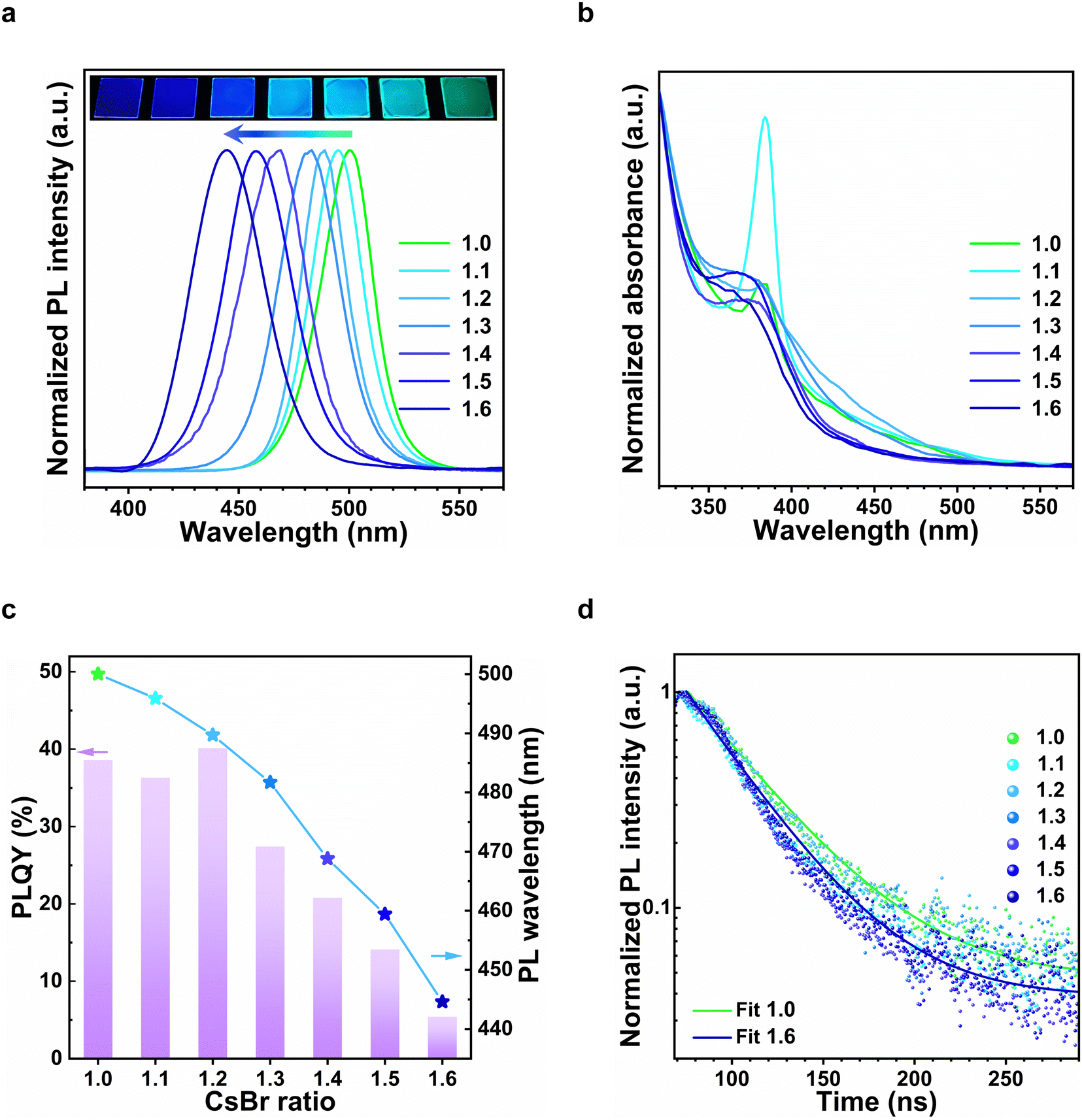 | ||
| Fig. 1 Characteristics of perovskite films with 3-APAB. (a) Normalized steady-state photoluminescence (PL) spectra and (b) UV-vis absorption spectra of thin films deposited with CsBr molar ratio varying from 1.0 to 1.6 in perovskite precursors (3-APAB:CsBr:PbBr2 = 1:x:1). (c) Combined PLQY and emission wavelength plots vs. CsBr molar ratio. (d) Time-resolved PL decay of perovskite samples with different CsBr molar ratio. | ||
To validate the importance of 3-APA+ in the formation of quantum-confined perovskite, we prepared a control sample using only CsBr and PbBr2 precursors under the same experimental conditions (Fig. S1, ESI†). The resulting CsPbBr3 perovskite film did not display any spectral blue-shift, and PL was observed at an expected 522 nm. In another control experiment, we prepared films using PbBr2 and 3-APAB, without any CsBr (see Fig. S2, ESI†). The films were not fluorescent, but showed an excitonic absorption peak at around 400 nm, which may be attributed to the formation of 2D perovskites.27 This experiment indicates that a perovskite framework containing Cs is still required for the formation of the quantum-confined blue-emitting samples.
Next, we evaluated the role and functionality of the ammonium group, the carboxylic acid group, as well as the 3-carbon backbone in the formation of the quantum-confined structure. In the first experiment, we employed n-propylammonium bromide (PAB) as ligands to replace 3-APAB (Fig. 2a). The photoluminescence blue-shifted moderately, but tapers off at around 486 nm. In the second experiment, we used propanoic acid as ligands in replacement of 3-APAB (Fig. 2b), and found that it was ineffective in providing any blue-shift to the perovskite samples. These experiments indicate that both the acid and the ammonium functional groups were required to achieve the desired quantum size control. Our FTIR spectral results also suggest that both the carboxylate and the ammonium groups interact with the perovskite surface (see Fig. S3, ESI†).
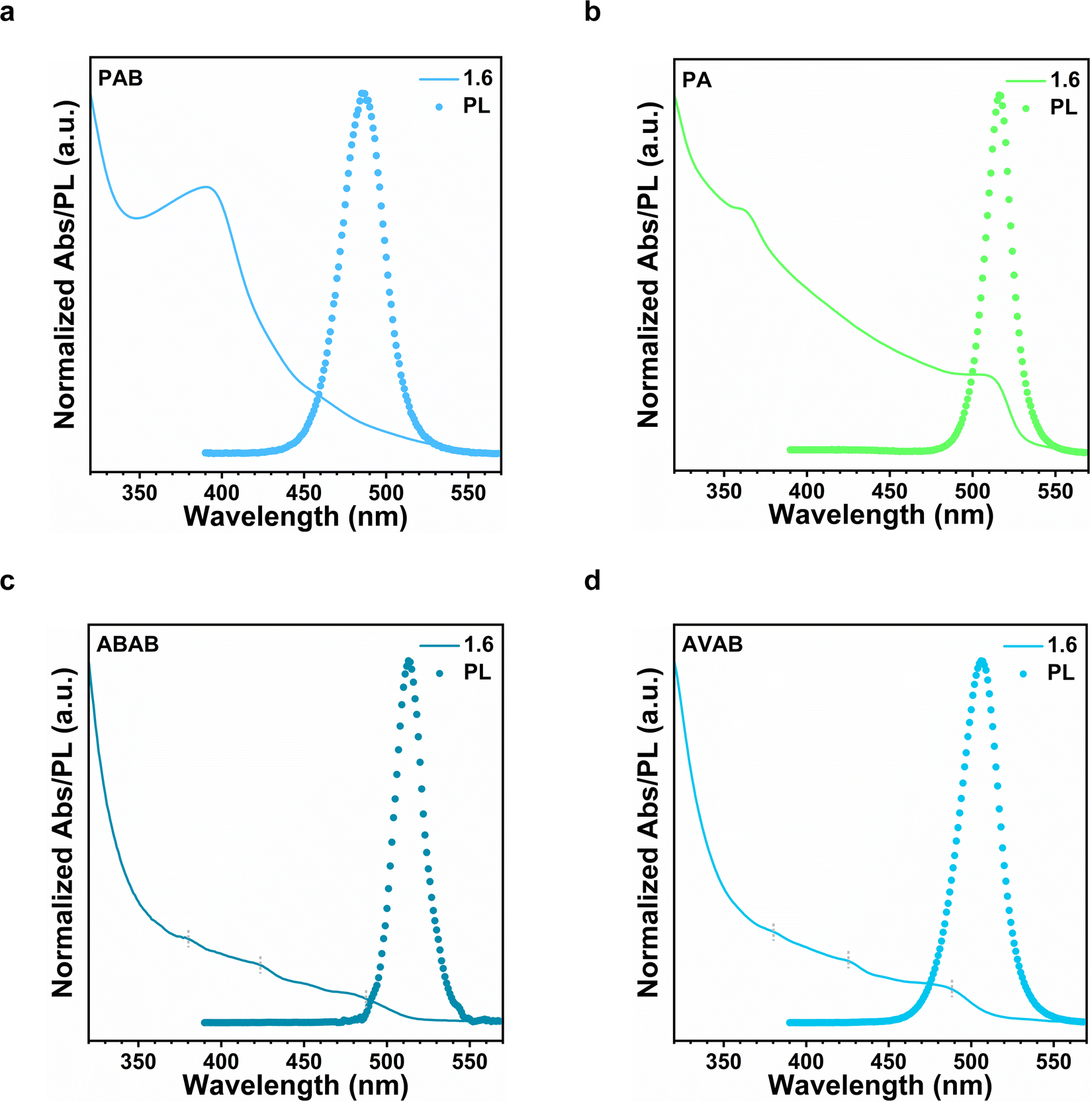 | ||
| Fig. 2 Control experiments with ligands replacing 3-APAB. The normalized steady photoluminescence (PL) and absorption spectra of perovskite films deposited with PAB (a), PA (b), ABAB (c), or AVAB (d) replacing 3-APAB as the ligand in the precursor solution. | ||
We then employed longer 4-ammonium butyric acid bromide (ABAB) and 5-ammonium valeric acid bromide (AVAB) as ligands (Fig. 2c and d) instead of 3-APAB. The PL peaks for samples were mildly blue-shifted to 513 nm for ABAB films and to 506 nm for AVAB films, respectively. These results indicate that a 3-carbon backbone served a critical function in the formation of the quantum-confined structures. We further note the appearance of several excitonic absorption peaks at ∼380, ∼424, and ∼488 nm in the films derived from ABAB or AVAB, which corresponds to quantum-well domains with different ‘n’ values in quasi-2D perovskites.18,26 This suggests that ABAB and AVAB would have stacked vertically between the quasi-2D perovskite layers, but this structural arrangement was not observed for the 3-APAB systems.
Based on the above-accumulated evidence, we reasoned that the 3-APAB anchors to the same perovskite crystal surface as a bidentate chelating ligand and restricted its growth, thus forming confined zero-dimensional domains within a continuous film. We therefore consider this structure as a quasi-zero-dimensional structure, as depicted in Fig. 3a. The excess CsBr served to provide CsBr-rich surfaces (or interfaces) for the perovskite nano-domains with high surface-to-bulk volume ratios.
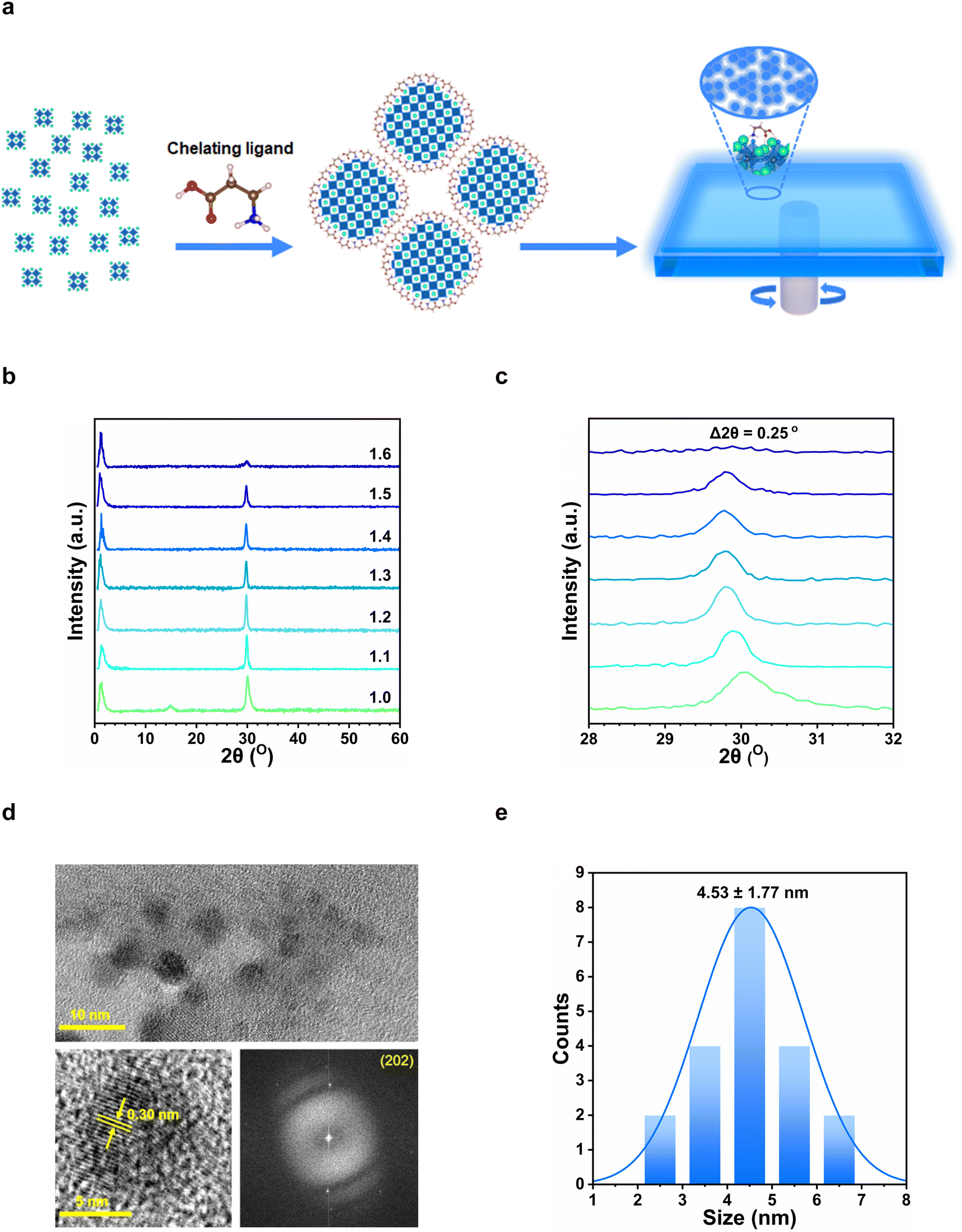 | ||
| Fig. 3 (a) Schematic diagram showing the formation of quasi-zero-dimensional nano-domains within perovskite films. Ball color represents: Cs (green), Pb (grey), Br (light blue), C (brown), N (blue), O (red), and H (white). (b) XRD patterns of CsPbBr3 films deposited on PVK coated silicon substrates. (c) Pseudo-Voight peak fitting of the diffraction peaks for the (202) crystallographic planes of thin films. (d) TEM image (top), high-magnification HRTEM images (bottom left) and SAED pattern (bottom right) of CsPbBr3 nano-domains formed with CsBr (1.4). (e) Size distribution histogram of CsPbBr3 nanocrystalline domains. | ||
In order to verify the structural characteristics of the perovskite films, we measured their X-ray diffraction (XRD) patterns, as shown in Fig. 3b. The distinctive XRD peaks at 14.9° and 30.1° can be indexed to the (101) and (202) planes for the orthorhombic Pnma CsPbBr3 phase. As the CsBr molar ratio increased from 1.0 to 1.6, the peak intensity at 30.1° decreased, which indicates a reduced crystallinity in the films (see Fig. S4, ESI† for TEM image comparison). The peaks were also slightly-shifted from 30.1° to smaller diffraction angles (Δ2θ ≈ 0.25° for the (202) planes), thus indicating a minor lattice expansion (Fig. 3c). This could be attributed to the incorporation of the 3-APA+ cation into the perovskite thin film, resulting in stresses and distortions to the perovskite structure. Notably, small angle diffraction peaks were also observed at ∼1.3° in all samples, which corresponds to domain sizes of approximately 7 nm. We consider these nanocrystalline domains within the bulk perovskite films to be responsible for the observed quantum confinement effects.
To directly visualize the nano-structural properties of these samples, we imaged the perovskite films using transmission electron microscopy (TEM). As shown in Fig. 3d, the CsPbBr3 perovskite exist as clusters that comprises quasi-spherical crystalline domains with sizes below 7 nm. Unlike colloidal perovskite nanocrystals, there was no well-defined spacing between crystal domains due to the absence of long-chain aliphatic ligands. The HRTEM image of a nano-domain revealed high crystallinity with a lattice spacing of ∼0.30 nm. The selected-area electron diffraction (SAED) showed the (202) crystalline plane, which is consistent with the XRD patterns of an orthorhombic CsPbBr3 phase.4 The average size of each CsPbBr3 nano-domain is approximately 4.5 nm, which is smaller than that of the exciton Bohr radius (∼7 nm), and thus accounts for the observed quantum size effects. The energy-dispersive X-ray spectroscopy (EDS) measurements further reveal a slight excess in CsBr (Cs:Pb:Br = 1.08:1:3.5), and thus suggest that CsBr with 3-APA+ lined the surfaces/interfaces of these nano-domains (Fig. S5, ESI†).
Based on the above experimental results, we constructed a model comprising perovskite with a CsBr-terminated surface that is coordinated to 3-APA+ in a pincer-shaped configuration (Fig. 4a). Our density functional theory (DFT) calculations on this model shows that the 3-carbon spaced 3-APA+ was particularly favorable in promoting the coordination of –NH3+ and –COOH to Br and Cs, respectively, and possess a high adsorption energy (Eads) of −4.49 eV. The pincer-shaped coordination is also further stabilized by the intramolecular hydrogen bond between –NH3+ and –COOH (Fig. 4a). In comparison, 3-APA+ in linear conformations were less-favorable for surface coordination, as indicated by their smaller Eads (see Fig. 4b–d).
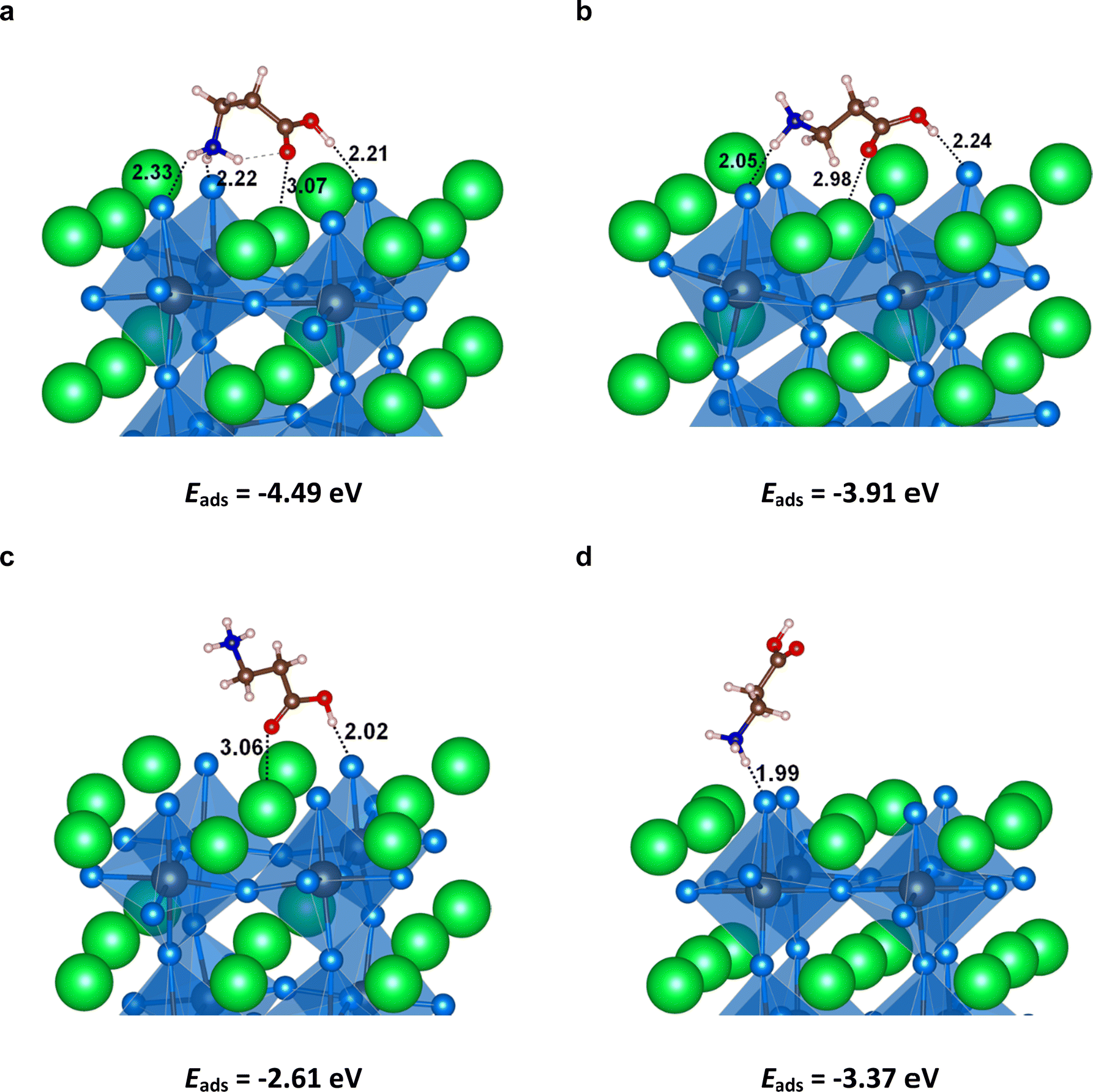 | ||
| Fig. 4 Adsorption geometry of 3-APA+ on Cs–Br terminated CsPbBr3(001) surface with different 3-APA+ conformation. (a) Pincer-shaped, (b) linear with –NH3+ and –COOH attached, (c) linear with –COOH attached, and (d) linear with –NH3+ attached. Dashed lines and numbers measure the bond length in unit of Å. Ball color represents: Cs (green), Pb (grey), Br (light blue), C (brown), N (blue), O (red), and H (white). Adsorption energy is shown in unit of eV. | ||
To demonstrate the generality of our approach, we introduced 3-APA+ into CsPbI3 perovskite, and attained a reasonably wide spectral tuning of its photoluminescence between near-infrared (NIR) (690 nm) and red (621 nm) (Fig. S6, ESI†). Similar to the case above, the XRD pattern show an orthorhombic CsPbI3 perovskite phase, as well as a slight lattice expansion upon the incorporation of 3-APA+ (Fig. S7, ESI†). The average size of the CsPbI3 nano-domains is approximately 5.0 nm (Fig. S7, ESI†).
As a demonstration of their functional application in electronic displays, we constructed perovskite light-emitting diodes (PeLEDs) using a glass/indium tin oxide (ITO)/NiOx/poly(9-vinlycarbazole)(PVK)/perovskite/2,4,6-Tris(3-(diphenylphosphinyl)phenyl)-1,3,5-triazine (PO-T2T)/LiF/Al device structure (see Fig. 5a). The CsPbBr3 PeLEDs displayed deep-blue electroluminescence at 468 nm, as shown in Fig. 5b. Fig. 5c shows the combined current density and luminance vs. voltage curves of the best-performing blue PeLED. A luminance of 6.72 cd m−2 is achieved at a current density of 0.81 mA cm−2, which corresponds to an external quantum efficiency (EQE) of 1.5% (Fig. S8, ESI†). The CsPbI3 counterpart offered saturated red electroluminescence at 638 nm (Fig. 5e). A red luminance of 28.15 cd m−2 is measured at a current density of 7.70 mA cm−2 (Fig. 5f), corresponding to an external quantum efficiency (EQE) of 2.0% (Fig. S9, ESI†). Notably, both our blue and red-emitting devices showed remarkable spectral stability across a broad range of driving voltages. These results suggest that the quasi-zero-dimensional perovskite structures are thermodynamically-stable, and do not suffer from field-induced ion migration, phase separation or aggregation effects. The Commission Internationale del’Eclairage (CIE) coordinate of the blue and red devices are (0.134, 0.065) and (0.705, 0.280) respectively, and are perfectly-suited for Rec.2020 compliant ultra-high definition color displays (Fig. 5d).
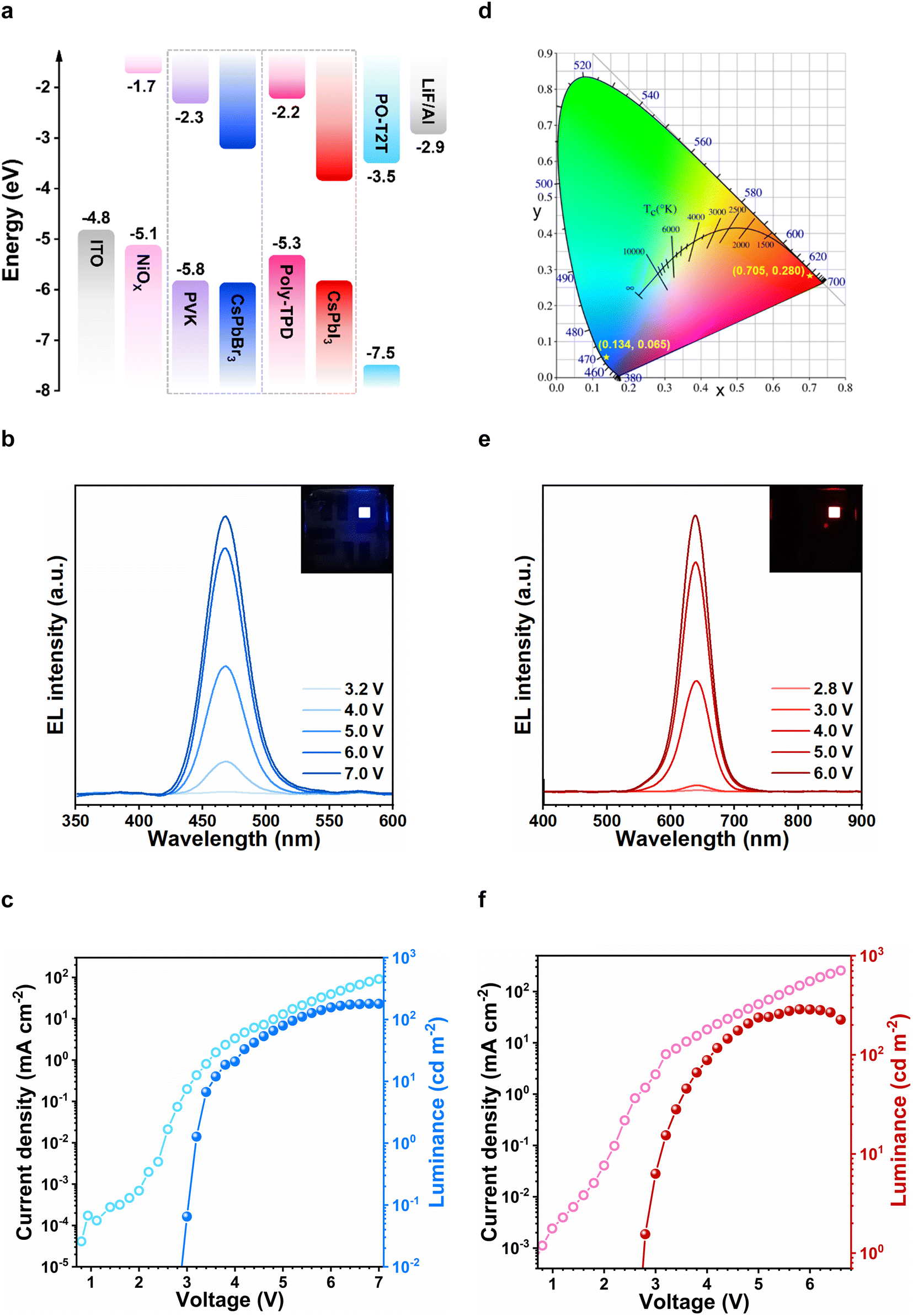 | ||
| Fig. 5 Optoelectronic characterization of the PeLED devices. (a) Energy-level diagram of as-fabricated blue and red PeLEDs. (b) EL spectra of blue PeLEDs recorded at various applied voltages (3.2–7.0 V). Inset shows a photo of blue PeLED device. (c) Current density–voltage–luminance (J–V–L) characteristics of blue PeLEDs. (d) CIE colour coordinates of the blue and red PeLEDs. (e) EL spectra of red PeLEDs recorded at various applied voltages (2.8–6.0 V). Inset shows a photo of red PeLED device. (f) Current density–voltage–luminance (J–V–L) characteristics of red PeLEDs. | ||
Conclusion
We have thus established a simple and effective approach to attain stable quantum-confinement in a new quasi-zero-dimensional perovskite structure. We show that a three-carbon amino acid was capable of creating size-tunable nano-domains within a bulk perovskite film, which allows versatile spectral tuning in both the bromide and the iodide-based perovskites. This strategy circumvents the spectral-stability challenges experienced in both mixed-halide perovskites and colloidal perovskite quantum dots, and could lead to important progress in electronic display applications.Conflicts of interest
The authors declare no completing financial interest.Acknowledgements
The authors thank the Agency for Science, Technology and Research (A*STAR) (A20E5c0088) and the Singapore Ministry of Education (MOE2019-T2-2-023) for funding support.Notes and references
- Z.-K. Tan, R. S. Moghaddam, M. L. Lai, P. Docampo, R. Higler, F. Deschler, M. Price, A. Sadhanala, L. M. Pazos, D. Credgington, F. Hanusch, T. Bein, H. J. Snaith and R. H. Friend, Bright light-emitting diodes based on organometal halide perovskite, Nat. Nanotechnol., 2014, 9, 687 CrossRef CAS PubMed.
- L. Protesescu, S. Yakunin, M. I. Bodnarchuk, F. Krieg, R. Caputo, C. H. Hendon, R. X. Yang, A. Walsh and M. V. Kovalenko, Nanocrystals of Cesium Lead Halide Perovskites (CsPbX3, X = Cl, Br, and I): Novel Optoelectronic Materials Showing Bright Emission with Wide Color Gamut, Nano Lett., 2015, 15, 3692 CrossRef CAS PubMed.
- G. Li, F. W. R. Rivarola, N. J. L. K. Davis, S. Bai, T. C. Jellicoe, F. de la Peña, S. Hou, C. Ducati, F. Gao, R. H. Friend, N. C. Greenham and Z.-K. Tan, Highly Efficient Perovskite Nanocrystal Light-Emitting Diodes Enabled by a Universal Crosslinking Method, Adv. Mater., 2016, 28, 3528 CrossRef CAS PubMed.
- Y. Liu, J. Cui, K. Du, H. Tian, Z. He, Q. Zhou, Z. Yang, Y. Deng, D. Chen, X. Zuo, Y. Ren, L. Wang, H. Zhu, B. Zhao, D. Di, J. Wang, R. H. Friend and Y. Jin, Efficient blue light-emitting diodes based on quantum-confined bromide perovskite nanostructures, Nat. Photonics, 2019, 13, 760 CrossRef CAS.
- Y. Dong, Y.-K. Wang, F. Yuan, A. Johnston, Y. Liu, D. Ma, M.-J. Choi, B. Chen, M. Chekini, S.-W. Baek, L. K. Sagar, J. Fan, Y. Hou, M. Wu, S. Lee, B. Sun, S. Hoogland, R. Quintero-Bermudez, H. Ebe, P. Todorovic, F. Dinic, P. Li, H. T. Kung, M. I. Saidaminov, E. Kumacheva, E. Spiecker, L.-S. Liao, O. Voznyy, Z.-H. Lu and E. H. Sargent, Bipolar-shell resurfacing for blue LEDs based on strongly confined perovskite quantum dots, Nat. Nanotechnol., 2020, 15, 668 CrossRef CAS PubMed.
- Z. Chu, Q. Ye, Y. Zhao, F. Ma, Z. Yin, X. Zhang and J. You, Perovskite Light-Emitting Diodes with External Quantum Efficiency Exceeding 22% via Small-Molecule Passivation, Adv. Mater., 2021, 33, 2007169 CrossRef CAS PubMed.
- Y. Cao, N. Wang, H. Tian, J. Guo, Y. Wei, H. Chen, Y. Miao, W. Zou, K. Pan, Y. He, H. Cao, Y. Ke, M. Xu, Y. Wang, M. Yang, K. Du, Z. Fu, D. Kong, D. Dai, Y. Jin, G. Li, H. Li, Q. Peng, J. Wang and W. Huang, Perovskite light-emitting diodes based on spontaneously formed submicrometre-scale structures, Nature, 2018, 562, 249 CrossRef CAS PubMed.
- K. Lin, J. Xing, L. N. Quan, F. P. G. de Arquer, X. Gong, J. Lu, L. Xie, W. Zhao, D. Zhang, C. Yan, W. Li, X. Liu, Y. Lu, J. Kirman, E. H. Sargent, Q. Xiong and Z. Wei, Perovskite light-emitting diodes with external quantum efficiency exceeding 20 per cent, Nature, 2018, 562, 245 CrossRef CAS PubMed.
- T. Chiba, Y. Hayashi, H. Ebe, K. Hoshi, J. Sato, S. Sato, Y.-J. Pu, S. Ohisa and J. Kido, Anion-exchange red perovskite quantum dots with ammonium iodine salts for highly efficient light-emitting devices, Nat. Photonics, 2018, 12, 681 CrossRef CAS.
- B. Zhao, S. Bai, V. Kim, R. Lamboll, R. Shivanna, F. Auras, J. M. Richter, L. Yang, L. Dai, M. Alsari, X.-J. She, L. Liang, J. Zhang, S. Lilliu, P. Gao, H. J. Snaith, J. Wang, N. C. Greenham, R. H. Friend and D. Di, High-efficiency perovskite–polymer bulk heterostructure light-emitting diodes, Nat. Photonics, 2018, 12, 783 CrossRef CAS.
- W. Xu, Q. Hu, S. Bai, C. Bao, Y. Miao, Z. Yuan, T. Borzda, A. J. Barker, E. Tyukalova, Z. Hu, M. Kawecki, H. Wang, Z. Yan, X. Liu, X. Shi, K. Uvdal, M. Fahlman, W. Zhang, M. Duchamp, J.-M. Liu, A. Petrozza, J. Wang, L.-M. Liu, W. Huang and F. Gao, Rational molecular passivation for high-performance perovskite light-emitting diodes, Nat. Photonics, 2019, 13, 418 CrossRef CAS.
- X. Zhao and Z.-K. Tan, Large-area near-infrared perovskite light-emitting diodes, Nat. Photonics, 2020, 14, 215 CrossRef CAS.
- Y.-H. Kim, S. Kim, A. Kakekhani, J. Park, J. Park, Y.-H. Lee, H. Xu, S. Nagane, R. B. Wexler, D.-H. Kim, S. H. Jo, L. Martínez-Sarti, P. Tan, A. Sadhanala, G.-S. Park, Y.-W. Kim, B. Hu, H. J. Bolink, S. Yoo, R. H. Friend, A. M. Rappe and T.-W. Lee, Comprehensive defect suppression in perovskite nanocrystals for high-efficiency light-emitting diodes, Nat. Photonics, 2021, 15, 148 CrossRef CAS.
- X. Gong, O. Voznyy, A. Jain, W. Liu, R. Sabatini, Z. Piontkowski, G. Walters, G. Bappi, S. Nokhrin, O. Bushuyev, M. Yuan, R. Comin, D. McCamant, S. O. Kelley and E. H. Sargent, Electron–phonon interaction in efficient perovskite blue emitters, Nat. Mater., 2018, 17, 550 CrossRef CAS PubMed.
- X. Zheng, S. Yuan, J. Liu, J. Yin, F. Yuan, W.-S. Shen, K. Yao, M. Wei, C. Zhou, K. Song, B.-B. Zhang, Y. Lin, M. N. Hedhili, N. Wehbe, Y. Han, H.-T. Sun, Z.-H. Lu, T. D. Anthopoulos, O. F. Mohammed, E. H. Sargent, L.-S. Liao and O. M. Bakr, Chlorine Vacancy Passivation in Mixed Halide Perovskite Quantum Dots by Organic Pseudohalides Enables Efficient Rec. 2020 Blue Light-Emitting Diodes, ACS Energy Lett., 2020, 5, 793 CrossRef CAS.
- M. Worku, Q. He, L.-J. Xu, J. Hong, R. X. Yang, L. Z. Tan and B. Ma, Phase Control and In Situ Passivation of Quasi-2D Metal Halide Perovskites for Spectrally Stable Blue Light-Emitting Diodes, ACS Appl. Mater. Interfaces, 2020, 12, 45056 CrossRef CAS PubMed.
- M. Yuan, L. N. Quan, R. Comin, G. Walters, R. Sabatini, O. Voznyy, S. Hoogland, Y. Zhao, E. M. Beauregard, P. Kanjanaboos, Z. Lu, D. H. Kim and E. H. Sargent, Perovskite energy funnels for efficient light-emitting diodes, Nat. Nanotechnol., 2016, 11, 872 CrossRef CAS PubMed.
- C. Wang, D. Han, J. Wang, Y. Yang, X. Liu, S. Huang, X. Zhang, S. Chang, K. Wu and H. Zhong, Dimension control of in situ fabricated CsPbClBr2 nanocrystal films toward efficient blue light-emitting diodes, Nat. Commun., 2020, 11, 6428 CrossRef CAS PubMed.
- D. Ma, P. Todorović, S. Meshkat, M. I. Saidaminov, Y.-K. Wang, B. Chen, P. Li, B. Scheffel, R. Quintero-Bermudez, J. Z. Fan, Y. Dong, B. Sun, C. Xu, C. Zhou, Y. Hou, X. Li, Y. Kang, O. Voznyy, Z.-H. Lu, D. Ban and E. H. Sargent, Chloride Insertion-Immobilization Enables Bright, Narrowband, and Stable Blue-Emitting Perovskite Diodes, J. Am. Chem. Soc., 2020, 142, 5126 CrossRef CAS PubMed.
- F. Yang, H. Chen, R. Zhang, X. Liu, W. Zhang, J. Zhang, F. Gao and L. Wang, Efficient and Spectrally Stable Blue Perovskite Light-Emitting Diodes Based on Potassium Passivated Nanocrystals, Adv. Funct. Mater., 2020, 30, 1908760 CrossRef CAS.
- E. T. Hoke, D. J. Slotcavage, E. R. Dohner, A. R. Bowring, H. I. Karunadasa and M. D. McGehee, Reversible photo-induced trap formation in mixed-halide hybrid perovskites for photovoltaics, Chem. Sci., 2015, 6, 613 RSC.
- D. Zhang, Y. Yu, Y. Bekenstein, A. B. Wong, A. P. Alivisatos and P. Yang, Ultrathin Colloidal Cesium Lead Halide Perovskite Nanowires, J. Am. Chem. Soc., 2016, 138, 13155 CrossRef CAS PubMed.
- J. Shamsi, D. Kubicki, M. Anaya, Y. Liu, K. Ji, K. Frohna, C. P. Grey, R. H. Friend and S. D. Stranks, Stable Hexylphosphonate-Capped Blue-Emitting Quantum-Confined CsPbBr3 Nanoplatelets, ACS Energy Lett., 2020, 5, 1900 CrossRef CAS PubMed.
- J. Leng, T. Wang, X. Zhao, E. W. Y. Ong, B. Zhu, J. D. A. Ng, Y.-C. Wong, K. H. Khoo, K. Tamada and Z.-K. Tan, Thermodynamic Control in the Synthesis of Quantum-Confined Blue-Emitting CsPbBr3 Perovskite Nanostrips, J. Phys. Chem. Lett., 2020, 11, 2036 CrossRef CAS PubMed.
- C. Sun, Y. Jiang, M. Cui, L. Qiao, J. Wei, Y. Huang, L. Zhang, T. He, S. Li, H.-Y. Hsu, C. Qin, R. Long and M. Yuan, High-performance large-area quasi-2D perovskite light-emitting diodes, Nat. Commun., 2021, 12, 2207 CrossRef CAS PubMed.
- S. Yuan, Z.-K. Wang, L.-X. Xiao, C.-F. Zhang, S.-Y. Yang, B.-B. Chen, H.-T. Ge, Q.-S. Tian, Y. Jin and L.-S. Liao, Optimization of Low-Dimensional Components of Quasi-2D Perovskite Films for Deep-Blue Light-Emitting Diodes, Adv. Mater., 2019, 31, 1904319 CrossRef CAS PubMed.
- M. Jiang, Z. Hu, Z. Liu, Z. Wu, L. K. Ono and Y. Qi, Engineering Green-to-Blue Emitting CsPbBr3 Quantum-Dot Films with Efficient Ligand Passivation, ACS Energy Lett., 2019, 4, 2731 CrossRef CAS.
Footnote |
| † Electronic supplementary information (ESI) available. See DOI: https://doi.org/10.1039/d2tc02077g |
| This journal is © The Royal Society of Chemistry 2022 |