
 Open Access Article
 This Open Access Article is licensed under a
 Creative Commons Attribution 3.0 Unported Licence
Rhodamine 6G and phloxine B as photosensitizers for inkjet-printed indium oxide phototransistors†
Liam
Gillan‡
 *a,
Fei
Liu‡
a,
Sanna
Aikio
b and
Jaakko
Leppäniemi
a
*a,
Fei
Liu‡
a,
Sanna
Aikio
b and
Jaakko
Leppäniemi
a
aVTT Technical Research Centre of Finland Ltd., Tietotie 3, Espoo, FI-02150, Finland. E-mail: liam.gillan@vtt.fi; fei.liu@vtt.fi; jaakko.leppaniemi@vtt.fi
bVTT Technical Research Centre of Finland Ltd, Kaitoväylä 1, Oulu, 90590, Finland. E-mail: sanna.aikio@vtt.fi
First published on 19th September 2022
Abstract
Indium oxide (In2O3) can be employed as an active semiconductor component in phototransistor devices. However, the large bandgap of In2O3 restricts its wavelength detection range to blue or UV light. Therefore, methods are required to facilitate detection of longer wavelengths. To this end, this work demonstrates the encapsulation of rhodamine 6G or phloxine B organic dye within a matrix of In2O3 semiconductor, to form a composite photosensitizing material that is patterned by the scalable fabrication pathway of inkjet-printing. This composite material is found to enhance the optoelectronic performance of inkjet-printed In2O3 thin film transistors in response to green light (565 nm). Specifically, the devices containing a rhodamine 6G/InOx composite top layer present good electrical performance in the dark with saturation mobility of 6.36 cm2 V−1 s−1 and, under green light illumination, photosensitivity of 4.1 × 10⁵, and responsivity of 250 A W−1. Its photoconductive state is returned to the initial condition by applied positive gate voltage pulse. The approach presented in this work could be applied for production of large area optoelectronics to enable applications such as displays, photo-memory, or dosimetry.
1. Introduction
Thin-film transistors (TFTs) based on metal oxide semiconductors benefit from optical transparency,1 flexibility,2 and high charge carrier mobility,3 with fabrication possible using low temperature4 and scalable processes such as printing.5 Oxide TFTs are known to experience voltage shift in response to incident photons,6 resulting in measurable changes to the drain current (Id), which enables their use as light detectors.7 However, many oxide semiconductors such as indium oxide (In2O3) have a large bandgap >3 eV which results in a wavelength detection range limited to blue or UV light.8 Therefore, methods are required to enable photosensitization for detection of longer wavelengths. Photoelectric performance of oxide phototransistors can be enhanced by charge carrier engineering,9,10 for instance, by exploiting metal oxides,8,11–15 perovskites,16–18 or quantum dots19–21 for photosensitization. Since first demonstrated in TiO2-based photovoltaics,22 photosensitizing of oxides with small molecule dyes has been broadly studied in dye-sensitized solar cells. Photosensitization of oxide transistors has been demonstrated with small molecule dyes such as chlorophyll-a,23 copper phthalocyanine,24 and D102.25,26 However, these reports have studied capping of the oxide semiconductor with photosensitizing agents. We propose an alternative approach of encapsulating the photosensitizing agent within a matrix of In2O3 semiconductor. Blending of In2O3 with organic species has previously been reported for tuning of charge transport properties, both through the organic/In2O3 composite material and as an interfacial layer between stacked material films.27–30 Inspired by these earlier reports, the motivation for the dye/InOx composite interlayer approach during this work was to (i) to protect the dye molecules from degradation due to direct exposure to air or mechanical delamination from the semiconductor surface, and (ii) indium oxide content providing atomic similarity, acting to improve interface characteristics such as charge injection to the In2O3 semiconductor channel.To realize practical applications for dye-sensitized oxide phototransistors, there is a need to develop scalable patterning methods for the dye layers, such as additive patterning by inkjet printing, to enable circuit integration of the phototransistors and large area fabrication.
In this work, we exploit the dyes rhodamine 6G (R6G) and phloxine B (PB) as photosensitizing agents for enhancing the optoelectronic performance of inkjet-printed In2O3 phototransistors. The dyes were inkjet patterned over the TFT channel region either intrinsically or encapsulated within an InOx matrix as composite materials. This work demonstrates that the inclusion of R6G and PB dyes increases the optoelectronic performance metrics of In2O3 TFTs in response to green light (565 nm used in this work), which is commonly emitted by the scintillator films used in indirect X-ray detectors,31 such as doped gadolinium oxysulfide. The combination of scalable patterning over large area and photosensitivity at 565 nm, renders the phototransistors applicable as sensing components such as dosimeters in flexible, large-area X-ray imaging.32,33
2. Results and discussion
Three key criteria were employed to guide the selection of organic dye to act as photosensitizing agent. (i) The lowest unoccupied molecular orbital (LUMO) of the dye should be higher than the conduction band minimum of In2O3 (−3.98 eV34). As depicted in Fig. 1a, this enables photo-induced electrons to be transferred from the LUMO of the dye to the In2O3 conduction band, resulting in increased TFT Id.35 (ii) The absorbance spectrum of the dye should exhibit large response to green light (specifically 565 nm, the source used during this study), because this is typically emitted by scintillator films used in indirect X-ray detectors and sits beyond the shorter wavelength region of blue to UV light where In2O3 is known to be intrinsically photosensitive.8 (iii) To enable patterning by inkjet printing, the dye must have sufficient solubility in a solvent vehicle with suitable viscosity and surface tension for stable ink droplet formation to produce a layer of material with continuous coverage after drying. A series of organic dyes are presented along with their relevant properties in Table S1 (ESI†). Based on the abovementioned criteria, R6G (LUMO = −3.14 eV36) and PB (LUMO = −2.64 eV37) were selected as the most suitable candidates from Table S1 (ESI†).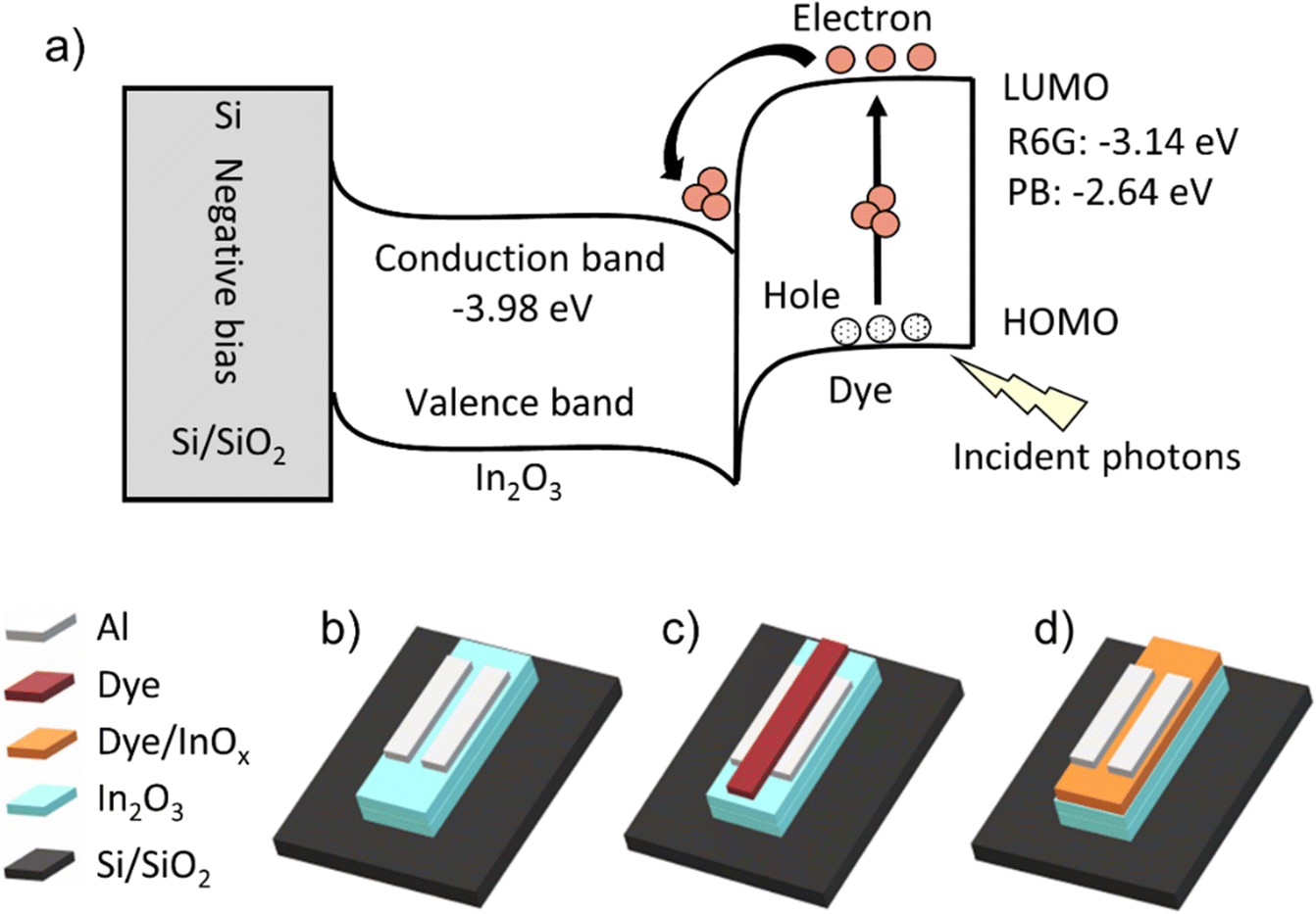 | ||
| Fig. 1 (a) Schematic band diagram depicting the photo-induced mechanism of electron transfer from the LUMO of the rhodamine 6G or phloxine B dye to the conduction band of the In2O3 semiconductor. (b–d) Illustrations (not to scale) of different TFT device configurations investigated during this work, including (b) reference dual layer inkjet-printed In2O3 structure, (c) TFT channel photosensitized by an overlayer film of inkjet-printed rhodamine 6G or phloxine B dye, and (d) rhodamine 6G or phloxine B dye/InOx photosensitizing composite material inkjet-printed between In2O3 semiconductor and Al source/drain contact electrodes. Each different architecture relies upon SiO2 as gate dielectric atop p-type Si gate electrode. | ||
Earlier reports on oxide-based phototransistors have typically studied the effects of applying discrete layers of photosensitizing agent, for instance as a capping layer over the oxide semiconductor material.16–21,24–26,38–41 In this work we also investigate this discrete layer approach by inkjet-patterning of dye over the TFT channel region (Fig. 1c). In parallel to this, we propose and study an alternative strategy of encapsulating the organic dye molecules within an InOx matrix, inkjet-printed as a composite interlayer between In2O3 semiconductor and source/drain top contact electrodes (Fig. 1d).
Fabrication of TFT devices requires consideration of thermal treatment following inkjet-patterning of inks containing the dyes. It is important to treat the inks with sufficient temperature to remove solvents and, in the case of the dye/InOx composite, ensure sufficient decomposition of materials such as nitrate from the indium nitrate hydrate reagent. However, given that the dyes are organic small molecules, elevated temperature could lead to thermal decomposition of the active photosensitizing agent. The inkjet-printed In2O3 semiconductor is known to start to perform when annealed at 250 °C, and performs optimally with at least 300 °C annealing temperature.42 Based on this, we identified annealing temperature of T1 = 70 °C for drying of bare dye containing inks dissolved in ethanol for devices shown in Fig. 1c. T2 = 200 °C and T3 = 250 °C were selected for investigating the curing of dye–InOx inks shown in Fig. 1d. Finally, T4 = 300 °C was selected for ensuring sufficient annealing of In2O3 component in dye/InOx composite inks shown in Fig. 1d. To assess whether thermal curing of the dye-containing inks would cause significant thermal decomposition of the dye constituents, thermal gravimetric analysis (TGA) was performed on solid R6G and PB powders, with results presented in Fig. 2a and b, respectively. R6G experienced the first major thermal decomposition event from around 220 °C to 275 °C, across T3, where mass loss was 9.8 wt%. The next major decomposition event occurred after T4, from around 300 °C to 375 °C, with mass loss of 17.2 wt% at 300 °C. PB mass loss at T1 was 2.4 wt%, increasing to 6.5 wt% at T2, then 6.8 wt% at T3, and slightly increasing further to 7.9 wt% at T4. These results suggest that the majority of both R6G and PB materials remain after thermal treatment at T1, T2, T3 or T4. However, the second decomposition event observed for R6G suggests that extended duration at 300 °C might lead to material degradation. This assertion was confirmed by further TGA analysis, ramping at 10 °C minute−1 up to 300 °C for R6G, and 250 °C for PB, with these temperatures held fixed for a period of 60 minutes. The results for R6G and PB are plotted in Fig. S1a and b (ESI†), respectively. For R6G, the mass loss when the temperature reached 300 °C was 21.6 wt%. After 5 minutes of fixed temperature, mass loss was 53.8 wt%, which further increased to 73.4 wt% after 10 minutes before stabilizing at around 75 wt% from around 11.5 minutes for the remaining 48 minutes. For PB, mass loss was 7.0 wt% at the start of the fixed 250 °C condition. This decreased marginally to 7.3 wt% after 5 minutes, 7.4 wt% after 10 minutes, and 8.1 wt% after the 60-minute period. Clearly the PB suffered less thermal degradation than the R6G, however even the R6G was not entirely decomposed even after one hour at 300 °C. It is possible that encapsulation of dye within the protective matrix of InOx would restrict exposure of dye material to air and thereby act to reduce the extent of thermal decomposition. Electrical measurements presented in later parts of this paper reveal that TFT devices performed best where dye/InOx composite films were processed at 250 °C for PB and 300 °C for R6G, so these were selected as thermal treatments for each material.
 | ||
| Fig. 2 Thermal gravimetric analysis at 10 °C minute−1 ramp rate in N2 of (a) rhodamine 6G and (b) phloxine B dye powders, with red lines marking ink annealing temperatures of T1 = 70 °C (a = 99.5 wt%, b = 97.6 wt%), T2 = 200 °C (a = 98.8 wt%, b = 93.5 wt%), T3 = 250 °C (a = 90.2 wt%, b = 93.2 wt%), and T4 = 300 °C (a = 82.8 wt%, b = 92.1 wt%). | ||
To investigate the properties of dye materials, films from bare dye and dye–InOx inks were spin-coated onto glass carrier substrates and studied with a series of characterization methods. Details of materials and processing steps for the spin-coated samples is provided in Table S2 (ESI†).
Surface morphology was studied by optical surface profilometry, with results presented in Fig. S2 (ESI†). Samples with InOx component annealed at 250 °C present greater average surface roughness (all >1.54 nm) than those annealed at 300 °C (all <0.75 nm). It is plausible that observed greater roughness in the lower temperature treated films due to insufficient thermal energy for complete conversion of precursors from the InOx ink component, resulting in films of insufficiently densified material, with greater porosity than films annealed at a higher temperature.29 This assertion is supported by observations of InOx ink precursor components in Fourier transform infrared (FTIR) analysis, as described below. The bare R6G dye film was observed to have the greatest roughness of all spin-coated films at 1.97 nm, much higher than the bare PB film of 0.45 nm. For both R6G/InOx and PB/InOx blends, the dye appeared to be mixed inside the InOx matrix with no sign of phase-separation or large agglomerates. Similarly, as for the reference device discussed above, the surface roughness was decreased when the annealing temperature was increased from 250 °C to 300 °C. This could indicate that the smoothening of dye/InOx films is also due to InOx ink precursor conversion. The lowest value of 0.14 nm was observed for R6G/InOx annealed at 300 °C indicating an ultra-smooth surface.
Homogenous amorphous phase is desirable for metal oxide semiconductor materials because it does not suffer from grain boundary scattering limitations of polycrystalline phase material.4 Grazing incidence X-ray diffraction (GIXRD) was performed on oxide-based films. Results shown in Fig. S3 (ESI†) reveal that the materials appeared amorphous in all cases, presenting no evidence of polycrystallinity, within the limit of the XRD analysis, induced by incorporation of R6G or PB dye materials in the oxide matrix.
Ultraviolet-visible absorbance spectroscopy (UV-Vis) of spin coated PB and R6G treated at 70 °C yielded signature peaks between 450 and 650 nm shown in Fig. 3a and b, which are in agreement with those in earlier reports on these materials.36,43–45 Bare InOx films treated at either 250 °C or 300 °C do not show absorbance peaks in this range. PB/InOx composite material treated at 250 °C exhibits absorbance peaks within the studied region, but with lesser peak magnitude than that of dye film treated at 70 °C. This reduced absorbance signal could be caused by partial thermal decomposition of the dye material, leading to reduced concentration of dye within the films. An absorbance peak is not seen from R6G/InOx composite material treated at 300 °C. It is plausible that the small quantities of dye present in the dye/InOx composite material samples (<4 wt% dye:In2O3) are insufficient to generate clear signal using the selected UV-Vis instrument, but the dye is present in sufficient quantities to act as a photoactive material that improves the optoelectronic performance of the In2O3 semiconductor.
 | ||
| Fig. 3 (a and b) UV-Vis absorbance spectra of films spin coated on glass. (c) FTIR spectra of spin coated films, annotated with peak assignments for the oxide-based materials. (d) Fluorescence intensity difference of samples to glass substrate reference under excitation wavelength of 532 nm with an emission filter at 570 nm. | ||
FTIR spectrum obtained from 250 °C treated InOx film (Fig. 3c) contains (i) broad O–H stretching signal around 3200 to 3600 cm−1, due to surface hydroxylation and/or adsorbed water, (ii) C–H stretching signal around 2700 to 2900 cm−1, which could arise from residual ethylene glycol solvent, (iii) O–H bending signal around 1500 to 1800 cm−1, from adsorbed water, (iv) N–O stretching signal around 1300 to 1500 cm−1, which is attributed to residual nitrate precursor.42,46 PB/InOx composite treated at 250 °C shows the same peaks as the 250 °C treated InOx film, but with slightly lower absorbance intensity. In agreement with our earlier observations,42,46 the magnitude of these absorbance signals greatly reduces when the InOx material is treated at a greater temperature of 300 °C (Fig. 3c) as the coated film shifts towards more complete precursor conversion to form In2O3. Presence of N–O stretching signal can be explained by the 15 minute thermal treatment being of insufficient duration for decomposition of the nitrate component of the precursor ink. The R6G/InOx material treated at 300 °C exhibits a very similar absorbance spectrum to the 300 °C treated InOx material. However, when viewing a more detailed narrow wavenumber range shown in Fig. S4 (ESI†), the R6G/InOx presents a slightly greater absorbance from 1800 to 1550 cm−1 than that of InOx, plausibly caused by presence of R6G because the pure dye presents peaks in this region. Fig. 3c shows that pure PB and R6G films treated at 70 °C present minor absorbance peaks at wavenumbers less than 1800 cm−1 and they do not present the C–H or O–H stretching signal seen from the oxide films at high wavenumbers due to absence of ethylene glycol (only ethanol was used to solubilize the pure dyes) and hydroxyl functionality, respectively. Fig. S4 (ESI†) presents absorbance peak assignments for PB and R6G films treated at 70 °C, which are in good agreement with spectra from earlier studies of the same materials.43,47–49
A series of films spin coated onto glass substrates (Table S2, ESI†) were analyzed by fluorescence measurements at a laser excitation wavelength of 532 nm, with an emission filter at 570 nm (Fig. 3d and Fig. S5, ESI†). This revealed that intrinsic InOx has a greater fluorescence intensity when annealed at 250 °C than when annealed at 300 °C, possibly caused by defects such as residual precursor materials when the film is incompletely cured. Inclusion of dye component in the films significantly increases the fluorescence intensity. Both PB and R6G containing films exhibit the same trend, where the largest intensity arises from dye/InOx composite annealed at 250 °C, followed by the pure dye, with the smallest intensity from dye/InOx composite annealed at 300 °C. Major decomposition of R6G was observed to occur at temperatures greater than 300 °C in TGA analysis (Fig. 2a), suggesting that a certain quantity of the dye material is likely to remain in spin coated films thermally treated at 300 °C for 15 min. This is supported by fluorescence analysis (Fig. 3d), where the measured intensity of R6G/InOx film annealed at 300 °C for 15 min is approximately double that of dye-free InOx with the same thermal treatment conditions.
TFT devices were fabricated with the structures illustrated in Fig. 1b–d, incorporating In2O3, dye/InOx, or bare dye components patterned by inkjet printing. The sample set includes PB and R6G dye/InOx composite films that were annealed at 200 °C, 250 °C, and 300 °C. Fig. 4 and Fig. S6 (ESI†) present current/voltage (I/V) transfer characteristics from sets of TFT devices of each different architecture shown in Fig. 1b–d measured in the dark, where the bias point of the phototransistor is identified as a gate voltage (Vg) point prior to the turn on voltage (Von), Vg = Von − 0.5 V, to ensure that the device is operating in the most sensitive subthreshold region. The drain current at the bias point is used as the dark current (Idark). The I/V metrics measured in the dark (without illumination) for each device type introduced in Fig. 1b–d are presented in Table 1. The devices with R6G/InOx and PB/InOx a layer had μsat of 6.36 cm2 V−1 s−1 and 2.70 cm2 V−1 s−1 and Vhyst 0.8 V and 1.1 V, respectively. Notably, the results indicate improved electrical characteristics for the devices incorporating dye/InOx blend, when compared to the reference devices μsat of 0.86 cm2 V−1 s−1 and Vhyst 2.0 V. As shown in Fig. S7 and Table S3 (ESI†), the semiconductor films were around 12.91 nm, 14.38 nm, and 17.97 nm thick for devices featuring a double layer In2O3 (reference), additional layer of R6G/InOx (R6G/InOx 300 °C), and additional layer of PB/InOx (PB/InOx 250 °C), respectively. Based on this, the improved performance could partly arise from to the increased semiconductor thickness,46 but also doping of the semiconductor by the organic dye molecules50 is possible and warrants further studies.
 | ||
| Fig. 4 Dark condition transfer measurements of a series of TFTs (left frames) with the dark current voltage listed for each device architecture being indicated by the vertical arrow, alongside average transfer measurements of the same series of TFTs (right frames) in response to 565 nm light over a range of intensities for (a) reference In2O3 TFTs, (b) In2O3 TFTs including a phloxine B/InOx photosensitizing layer, and (c) In2O3 TFTs including a rhodamine 6G/InOx photosensitizing layer. | ||
| Device type | n (TFTs) | V hyst (V) | μ sat (cm2 V−1 s−1) | I on/off | V on (V) |
|---|---|---|---|---|---|
| Reference In2O3 | 7 | 2.0 ± 0.2 | 0.86 ± 0.15 | ∼107 | −1.8 ± 0.3 |
| R6G bare dye | 5 | 1.9 ± 0.1 | 0.55 ± 0.06 | ∼107 | −1.8 ± 0.5 |
| PB bare dye | 8 | 1.6 ± 0.2 | 0.71 ± 0.12 | ∼106 | −1.6 ± 0.1 |
| R6G/InOx 300 °C | 7 | 0.8 ± 0.4 | 6.36 ± 1.22 | ∼106 | −2.5 ± 0.8 |
| PB/InOx 250 °C | 7 | 1.1 ± 0.1 | 2.70 ± 0.17 | ∼105 | −1.2 ± 0.2 |
I/V behavior of the TFT devices was studied in response to varying intensity (1.4 μW cm−2 to 1.41 mW cm−2) of incident photons from 565 nm wavelength light source, with results presented in Fig. 4 and Fig. S6 (ESI†). Here, the general observed trend is a negative shift of the Von in response to increasing light intensity, thus indicating an increasing charge carrier concentration in the In2O3 semiconductor channel in response to increasing light intensity. This observation can be explained by the mechanism illustrated in Fig. 1, where photo-induced electrons are transferred from the LUMO level of the dye to the conduction band of the In2O3. The bare dye devices (Fig. S6a and b, ESI†) present a greater degree of Von shift than that of the dye/InOx composite devices (Fig. 4b, c, and Fig. S6c–f, ESI†) in tandem with a slight increase in the off current (Ioff) for increasing light intensity, in agreement with earlier reports for bare dye on top of oxide semiconductor channel.29 The least degree of photo-induced change in Von is observed from PB/InOx composite devices annealed at 300 °C (Fig. S6d, ESI†). Notably, the reference In2O3 devices with an absence of photosensitizer dye (Fig. 4a) only presents a marginal change in I/V characteristics, even after illumination with the highest intensity light (1.41 mW cm−2). Dark current measurements from dye/InOx composite devices annealed at 200 °C (Fig. S6c and e, ESI†) as well as R6G/InOx composite devices annealed at 250 °C (Fig. S6f, ESI†) display poor performance with high inter-device variability in Von and on-current level that can be attributed to incomplete annealing of the In2O3 component of the composite. Furthermore, the large variation in the Von with very negative values for some of the devices would prevent finding a common bias point that could lead to optimal photodetector circuit operation with all the phototransistors at the subthreshold region. For example, some of the PB/InOx devices annealed at 200 °C (Fig. S6c, ESI†) appear to suffer from Von at very large negative Vg beyond −20 V. Due to this poor electrical performance, dye/InOx devices annealed at 200 °C, R6G/InOx devices annealed at 250 °C (Fig. S6f, ESI†), and the PB/InOx annealed at 300 °C (Fig. S6d, ESI†) exhibiting limited photo induced current shift were excluded from comparison of optoelectronic performance metrics with other devices. The optimal condition in terms of response to green light was found to be 250 °C for PB/InOx and 300 °C for R6B/InOx shown in Fig. 4b and c, respectively, where the devices exhibit clear response to varied light intensities and show low inter-device variation with consistent, slightly negative Von that would allow assigning a common bias point. The optoelectronic performance of these optimal devices were studied in more detail in the following section.
Earlier reports have shown that incomplete annealing of an additional semiconductor film layer can enhance optoelectronic properties of oxide TFTs.8,11 To confirm that this is not the case with our devices and that the observed improvement in optoelectronic properties can be attributed to inclusion of dye, TFTs were fabricated by the same processing conditions as those with dye/InOx films, but incorporating a film of In2O3 annealed at 250 °C or 300 °C in place of dye/InOx. I/V characteristics presented in Fig. S8 (ESI†) reveal that there is not a significant improvement in optoelectronic performance due to the additional layer of In2O3 when the dye is absent.
Two parameters that are commonly employed to describe the optoelectronic performance of phototransistors are photosensitivity (PS) and responsivity (R). PS is defined as the current change which is normalized to the dark current (Idark) according to
 | (1) |
 | (2) |
 | ||
| Fig. 5 Optoelectronic figures of merit (a) photosensitivity, and (b) responsivity. | ||
Persistent photoconductivity (PPC) is a phenomenon where photo-induced current shift remains in metal oxide semiconductors even after the illumination event has ceased.10Fig. 6a reveals evidence for PPC in both In2O3 reference and R6G/InOx devices. Here, dashed lines indicate that the Idark for In2O3 is 1.1 × 10⁻¹² A at Vg = −2 V, and for R6G/InOx it is 5.9 × 10⁻¹² A at Vg = −7.5 V. In response to 8 minutes illumination, dotted lines in Fig. 6a illustrate how Idark increases to Ilight 1.4 × 10⁻¹⁰ A for In2O3, and 9.4 × 10⁻⁹ A for R6G/InOx. Once the illumination source is deactivated, there is gradual reduction in Ilight towards Idark for each device. Presence of defect states in a metal oxide semiconductor material can influence PPC. For instance, oxygen vacancies (Vo) in the In2O3 film may become ionized by incident photons to Vo+ or Vo++, forming defect trap sites. Ionized Vo generate electrons which cause the energy of the defect states to increase towards the conduction band of In2O3, leading to increased channel conductivity which may be observed as PPC.52,53 However, this explanation applies to intrinsic In2O3 and photoexcitation with sufficiently low wavelength (<∼400 nm).13 Moreover, as the exact origin for the PPC in oxide semiconductors and the mechanisms leading to its decay are not fully understood,54 especially the contribution of dye-sensitization to the PPC remains, to a great extent, unexplored.55
 | ||
| Fig. 6 (a) Illumination induced drain current (Id) shift from dark state to illuminated state, then gradual decay towards original dark state condition. (b) Increased Id of a R6G/InOx device in response to 3 V LED illumination at 1.41 mW cm−2, followed by sequential applied gate voltage pulses of 20 V, 30 V, and 40 V in an attempt to decrease Id back to dark state condition. | ||
Fig. 6a shows that for both device types, the decay is not sufficient for Id to reach Idark even after more than 3 days (2.79 × 10⁵ seconds) duration. This suggests that PPC might influence the results shown in Fig. 4, by contributing a cumulative effect to shift in Id. To investigate the extent of this cumulative PPC effect, a R6G/InOx device was subjected to sequential repeat measurements at 5 different illumination intensities covering the range from Fig. 4. Results presented in Fig. S10 (ESI†) show that higher light intensities of 141 μW cm−2 and 1410 μW cm−2 do cause a shift towards more negative Vg, with the effect appearing to saturate with repeated measurements. However, as a single I/V measurement was performed for each illumination condition in order of increasing intensity on a single device to generate data for Fig. 4, any cumulative effects are expected to be negligible.
One common strategy for alleviating PPC in oxide semiconductors is by applying a positive Vg pulse gathering electrons towards the gate dielectric, to encourage recombination of localized holes at ionized Vo (Vo+ and Vo++) and achieve neutral Vo.7,12,56,57Fig. 6b presents observed effects of a series of 3 second duration applied positive Vg pulses on Id of a R6G/InOx device after excitation by high intensity (1.41 mW cm−2) LED illumination (565 nm). The photo-induced exited state resulting from 10 seconds illumination is around Ilight = 7 × 10⁻¹⁰ A. The measured Id decays to almost 5 × 10⁻¹⁰ A during the 10 seconds after illumination is stopped. Then a pulse of Vg = 20 V is applied which reduces Id to below 1 × 10⁻¹⁰, but is not sufficient to reduce Id to the initial Idark of around 1 × 10⁻¹¹. A second higher energy Vg pulse of 30 V reduces Id to below that achieved using a Vg pulse of 20 V, however a third Vg pulse of 40 V was required to force recombination and return the device to a condition similar to that of initial dark state. It is known that sufficiently high electric field in the form of Vg pulse (>2 MV cm−1) can be needed for resetting of oxide phototransistors.12,56 The need here for a large electric field of ∼4 MV cm−1 to erase the PPC, as observed in Fig. 6b, could arise from the dye/InOx composite layer residing on top of the device, thus further away from the semiconductor-dielectric interface. Positive Id creep follows the Vg pulses in Fig. 6b. This can likely be attributed to negative bias stress where the measurement is undertaken using parameters of Vd = 2 V and Vg = −15.5 V.
The device reset process for alleviating PPC facilitates resettable operation that could enable diverse applications including wearable healthcare,58 displays,7 or erasable photo memory,59 as outlined in a recent review article,10 whereas the long retention due to PPC could allow exploitation in personal dosimetry.32
3. Conclusions
This work advances oxide phototransistors by exploiting phloxine B (PB) and rhodamine 6G (R6G) organic dyes as photosensitizing agents demonstrated to boost optoelectronic performance of In2O3 TFTs. The operation range was extended beyond the typical UV/blue wavelength region for In2O3, to include green light (565 nm). PB and R6G photosensitizing agents were patterned by inkjet-printing both as an intrinsic layer of dye material and as a composite with the dye encapsulated in an InOx matrix. Optoelectronic properties were particularly improved by incorporating a R6G/InOx composite interlayer, which exhibits photosensitivity of 4.1 × 10⁵ and responsivity of 250 A W−1. The observed persistent photoconductive state could be erased by applying a positive gate voltage pulse. The solution-based deposition route for the composite photosensitizer material enables additive patterning that would be challenging to realize using sputtering deposition methods. Furthermore, print-patterning of devices by inkjet process is a scalable patterning pathway towards circuit integration of the phototransistor components and large area fabrication. Potential opportunities that may be enabled by this work include applications in imaging, dosimetry, biotechnology and photo memory.4. Experimental
In2O3 precursor inks were prepared under nitrogen atmosphere by dissolving indium nitrate hydrate (In(NO3)3 × 2.5H2O, Epivalence UK) in 2-methoxyethanol (anhydrous, 99.8%, Sigma-Aldrich) to 0.2 M by stirring for 17.5 h at 75 °C, before filtration through 0.2 μm polytetrafluoroethylene (PTFE) Acrodisc, then finally adding 10 wt% of ethylene glycol (anhydrous, 99.8%, Sigma-Aldrich). For dye/In2O3 composite inks, rhodamine 6G (99%, Acros Organics) or phloxine B (85%, Biological stain, Acros Organics) was added to In2O3 precursor ink at 1 mg mL−1 and dissolved using vortex mixing. Dye inks were prepared by adding 10 mg of rhodamine 6G (99%, Acros Organics) or phloxine B (85%, Biological stain, Acros Organics) into 10 mL ethanol (99.5%, ETAX, Altia Industrial) under nitrogen atmosphere and dissolving with magnetic stirring at RT, before adding 10 vol% ethylene glycol (Anhydrous, 99.8%, Sigma-Aldrich) and stirring to mix.For thermogravimetric analysis, dye powders were heated at 10 °C min−1 ramp rate from 30 °C to 250 °C, 300 °C, or 500 °C in nitrogen using a TA Instruments TGA Q500.
Table S2 (ESI†) summarizes the processing of samples spin coated during this work. Prior to spin coating, glass substrates were cleaned sequentially at 45 °C in an ultrasonic bath with deionized water, acetone, and isopropanol. Cleaned substrates were plasma-treated (1 min, 0.2 mbar, O2, 200 W, Diener Nano) immediately prior to spin coating at 1500 krpm for 60 s (Laurell, WS-400B6NPP/LITE). Spin-coated inks were thermally treated on a hotplate in air.
For inkjet printing, In2O3 and dye/In2O3 composite inks were mixed for 15 min, before filtration (0.2 μm PTFE) into a piezoelectric cartridge (30 °C, DMC-11610) and inkjet patterned onto plasma-treated surface (1 min, 0.2 mbar, O2, 200 W, Diener Nano) from 7 adjacent nozzles (7 m s−1, 75 μm drop spacing, 339 dpi) with a Fujifilm Dimatix DMP 2831 printer, using a trapezoidal waveform. Printed inks were thermally treated on a hotplate in air. In2O3 was dried (15 min, 130 °C) and then annealing (30 min, 300 °C). Dye blends were annealed for 15 min at either 250 °C (PB/InOx), or 300 °C (R6G/InOx). The pure dye inks were mixed for 10 min by stirrer table and then loaded into a piezoelectric cartridge (DMC-11610, 10 pL) using a 1.0 μm PTFE filter. Plasma treatment (12 s, 0.2 mbar, Ar, 200 W, Diener Nano) was carried out on the In2O3 TFTs for both dyes (rhodamine 6G and phloxine B). For Rhodamine 6G dye ink, one layer was printed from 2 adjacent nozzles (5 m s−1, 38 μm drop spacing). After printing, the sample was heated (15 min, 70 °C) on a hot plate for drying. For phloxine B dye ink, two consecutive layers without time delay between two-layer printing were printed from 4 adjacent nozzles (5 m s−1, 38 μm drop spacing). The printed ink was thermally heated under the same drying condition (15 min, 70 °C) as the printed rhodamine 6G dye ink. Both dye inks were inkjet printed with a Fujifilm Dimatix DMP 2831 printer, using a trapezoidal waveform.
TFTs were fabricated with bottom-gate architecture composed of 625 μm thick p-type Si as gate electrode with ∼100 nm of thermally grown SiO2 dielectric and dual layer inkjet-printed In2O3 semiconductor as previously reported.46 Dye/In2O3 composite films were inkjet-printed as a single layer, directly onto In2O3 semiconductor of the same pattern. A customized shadow mask enabled patterning of Al source/drain electrodes (60 nm thick) by resistive evaporation, providing a channel length of 80 μm (L) and width (W) of 1 mm (W/L ≈ 12.5).
Optical profiling for obtaining surface roughness and film thickness was performed using a Sensofar S Neox 3D profiler in phase-shifting interferometry mode. Attenuated total reflection Fourier transform infrared (ATR-FTIR) spectra were obtained using a ThermoScientific Nicolet S50i with a Ge crystal and a grazing angle ATR accessory (Harrick Scientific Products Inc. VariGATR). Grazing incidence X-ray diffraction (GIXRD) was performed with a 0.5° incidence angle, using a PANalytical X’Pert PRO MRD and Cu Kα X-ray source. Ultraviolet-visible (UV-Vis) spectra were generated with an Avantes spectrophotometer (AvaSpec-2048 × 14 USB2) and halogen source (AvaLight-DHS), using glass substrate as a reference. Fluorescence intensity was measured with a scanner (Amersham Typhoon RGB, GE Healthcare) using an excitation laser wavelength of 532 nm, emission filter 570BP20, photo multiplier tube voltage 500 V, and a pixel size of 200 μm. Fluorescence intensities were analyzed using ImageQuant TL Toolbox version 8.1 software (GE Healthcare). For each sample, fluorescence intensity was calculated as an average value within the area shown by the green rectangle (width 20 and height 18 pixels) in Fig. S5 (ESI†). Representative area, e.g. an area without visible contamination such as dust or tape on the sample backside, was chosen for the analysis from each sample. Untreated glass sample acted as a reference, and the fluorescence intensity differences of the processed samples to untreated glass were calculated. Electrical characterization of TFTs was performed with a Keithley 4200 SCS at room temperature in air. Photo measurements with varying light intensity (0 μW cm−2, 1.4 μW cm−2, 4.2 μW cm−2, 14.1 μW cm−2, 42.3 μW cm−2, 141 μW cm−2, 423 μW cm−2 and 1.41 mW cm−2) were performed using a green LED light source at ∼10.5 cm distance (565 nm nominal peak intensity with 104 nm bandwith, M565L3, Thorlabs). For results presented in Fig. 4, Fig. S7 and S8 (ESI†), a 30 s time delay was applied between sequential measurements. Samples were stored in the dark overnight to recover from the excited illuminated state to ground dark state.
Author contributions
L. G. and F. L. contributed equally to this work. J. L. supervised the work. J. L., L. G., and F. L. conceived the idea. All authors designed the experiments. L. G. and F. L. fabricated the samples and performed the experiments, except fluorescence which was performed by S. A. The first draft manuscript was prepared by L. G. and F. L. All authors reviewed the manuscript.Conflicts of interest
The authors declare no conflict of interest.Acknowledgements
The work was funded in part by the Academy of Finland project FLEXRAD (Grant Agreement No. 328627) and the Business Finland co-innovation project RaPtor (Grant Agreement No. 6030/31/2018). Technical assistance from Mrs Pirjo Hakkarainen is gratefully acknowledged.References
- K. Nomura, H. Ohta, K. Ueda, T. Kamiya, M. Hirano and H. Hosono, Thin-Film Transistor Fabricated in Single-Crystalline Transparent Oxide Semiconductor, Science, 2003, 300(5623), 1269–1272, DOI:10.1126/science.1083212.
- Y. H. Kim, et al., Flexible metal-oxide devices made by room-temperature photochemical activation of sol–gel films, Nature, 2012, 489(7414), 128–132, DOI:10.1038/nature11434.
- H. Q. Chiang, J. F. Wager, R. L. Hoffman, J. Jeong and D. A. Keszler, High mobility transparent thin-film transistors with amorphous zinc tin oxide channel layer, Appl. Phys. Lett., 2005, 86(1), 013503, DOI:10.1063/1.1843286.
- K. Nomura, H. Ohta, A. Takagi, T. Kamiya, M. Hirano and H. Hosono, Room-temperature fabrication of transparent flexible thin-film transistors using amorphous oxide semiconductors, Nature, 2004, 432, 488–492, DOI:10.1038/nature03090.
- D.-H. Lee, Y.-J. Chang, G. S. Herman and C.-H. Chang, A General Route to Printable High-Mobility Transparent Amorphous Oxide Semiconductors, Adv. Mater., 2007, 19(6), 843–847, DOI:10.1002/adma.200600961.
- W. T. Chen, H. W. Hsueh, H. W. Zan and C. C. Tsai, Light-enhanced bias stress effect on amorphous In–Ga–Zn–O thin-film transistor with lights of varying colors, Electrochem. Solid-State Lett., 2011, 14(7), H297, DOI:10.1149/1.3584088.
- S.-E. Ahn, et al., Metal Oxide Thin Film Phototransistor for Remote Touch Interactive Displays, Adv. Mater., 2012, 24(19), 2631–2636, DOI:10.1002/adma.201200293.
- J. Chung, Y. J. Tak, W.-G. Kim, B. H. Kang and H. J. Kim, Artificially Fabricated Subgap States for Visible-Light Absorption in Indium–Gallium–Zinc Oxide Phototransistor with Solution-Processed Oxide Absorption Layer, ACS Appl. Mater. Interfaces, 2019, 11(42), 38964–38972, DOI:10.1021/acsami.9b14154.
- W. Ouyang, F. Teng, J. H. He and X. Fang, Enhancing the Photoelectric Performance of Photodetectors Based on Metal Oxide Semiconductors by Charge-Carrier Engineering, Adv. Funct. Mater., 2019, 29(9), 1807672, DOI:10.1002/adfm.201807672.
- H. Yoo, I. S. Lee, S. Jung, S. M. Rho, B. H. Kang and H. J. Kim, A Review of Phototransistors Using Metal Oxide Semiconductors: Research Progress and Future Directions, Adv. Mater., 2021, 33(47), 2006091, DOI:10.1002/ADMA.202006091.
- Y. J. Tak, J. Chung, Y. Kim, W.-G. Kim, B. H. Kang and H. J. Kim, Indium Gallium Zinc Oxide based Phototransistor for Visible Light Detection by Stacking Solution Processed Defective Oxide Layer, SID Symp. Dig. Tech. Pap., 2017, 48(1), 1353–1355, DOI:10.1002/sdtp.11895.
- B. H. Kang, W.-G. Kim, J. Chung, J. H. Lee and H. J. Kim, Simple Hydrogen Plasma Doping Process of Amorphous Indium Gallium Zinc Oxide-Based Phototransistors for Visible Light Detection, ACS Appl. Mater. Interfaces, 2018, 10(8), 7223–7230, DOI:10.1021/acsami.7b17897.
- G. Han, S. Cao, Q. Yang, W. Yang, T. Guo and H. Chen, High-Performance All-Solution-Processed Flexible Photodetector Arrays Based on Ultrashort Channel Amorphous Oxide Semiconductor Transistors, ACS Appl. Mater. Interfaces, 2018, 10(47), 40631–40640, DOI:10.1021/acsami.8b14143.
- D.-B. Ruan, et al., Photoresponsivity Enhancement and Extension of the Detection Spectrum for Amorphous Oxide Semiconductor Based Sensors, Adv. Electron. Mater., 2019, 5(3), 1800824, DOI:10.1002/aelm.201800824.
- D. Kim, Y. Kim, B. H. Kang, J. H. Lee, J. Chung and H. J. Kim, Fabrication of indium gallium zinc oxide phototransistors via oxide-mesh insertion for visible light detection, J. Mater. Chem. C, 2020, 8, 165–172, 10.1039/C9TC04982G.
- S. Du, et al., Oxide Semiconductor Phototransistor with Organolead Trihalide Perovskite Light Absorber, Adv. Electron. Mater., 2017, 3(4), 1600325, DOI:10.1002/aelm.201600325.
- L. Yan, X. Du, C. Liu, S. Zhang and H. Zhou, Narrow Bandgap Pb–Sn Perovskites/InGaZnO Hybrid Phototransistors for Near-Infrared Detection, Phys. Status Solidi, 2019, 216(23), 1900417, DOI:10.1002/pssa.201900417.
- S. Wei, et al., Flexible Quasi-2D Perovskite/IGZO Phototransistors for Ultrasensitive and Broadband Photodetection, Adv. Mater., 2020, 32(6), 1907527, DOI:10.1002/adma.201907527.
- X. Liu, et al., Photo-modulated thin film transistor based on dynamic charge transfer within quantum-dots-InGaZnO interface, Appl. Phys. Lett., 2014, 104(11), 113501, DOI:10.1063/1.4868978.
- S. M. Lee, et al., Enhanced photocurrent of Ge-doped InGaO thin film transistors with quantum dots, Appl. Phys. Lett., 2015, 106(3), 031112, DOI:10.1063/1.4906423.
- X. Liu, et al., Narrow-Band QD-Enhanced PIN Metal-Oxide Heterostructure Phototransistor with the Assistance of Printing Processes, Adv. Opt. Mater., 2020, 8(4), 1901472, DOI:10.1002/adom.201901472.
- B. O’Regan and M. Grätzel, A low-cost, high-efficiency solar cell based on dye-sensitized colloidal TiO2 films, Nature, 1991, 353(6346), 737–740, DOI:10.1038/353737a0.
- H.-C. Wu, et al., Photoinduced Electron Transfer in Dye-Sensitized SnO2 Nanowire Field-Effect Transistors, Adv. Funct. Mater., 2011, 21(3), 474–479, DOI:10.1002/adfm.201001521.
- J. Li, et al., Enhanced photosensitivity of InGaZnO-TFT with a CuPc light absorption layer, Superlattices Microstruct., 2012, 51(4), 538–543, DOI:10.1016/j.spmi.2012.02.002.
- P. Pattanasattayavong, S. Rossbauer, S. Thomas, J. G. Labram, H. J. Snaith and T. D. Anthopoulos, Solution-processed dye-sensitized ZnO phototransistors with extremely high photoresponsivity, J. Appl. Phys., 2012, 112(7), 074507, DOI:10.1063/1.4757602.
- A. D. Mottram, Y. H. Lin, P. Pattanasattayavong, K. Zhao, A. Amassian and T. D. Anthopoulos, Quasi Two-Dimensional Dye-Sensitized In2O3 Phototransistors for Ultrahigh Responsivity and Photosensitivity Photodetector Applications, ACS Appl. Mater. Interfaces, 2016, 8(7), 4894–4902, DOI:10.1021/acsami.5b11210.
- W. Huang, et al., Metal Oxide Transistors via Polyethylenimine Doping of the Channel Layer: Interplay of Doping, Microstructure, and Charge Transport, Adv. Funct. Mater., 2016, 26(34), 6179–6187, DOI:10.1002/adfm.201602069.
- L. Gillan, J. Leppäniemi, K. Eiroma, H. Majumdar and A. Alastalo, High performance solution processed oxide thin-film transistors with inkjet printed Ag source–drain electrodes, J. Mater. Chem. C, 2018, 6(13), 3220–3225, 10.1039/c7tc05679f.
- L. Gillan, S. Li, J. Lahtinen, C. H. Chang, A. Alastalo and J. Leppäniemi, Inkjet-Printed Ternary Oxide Dielectric and Doped Interface Layer for Metal-Oxide Thin-Film Transistors with Low Voltage Operation, Adv. Mater. Interfaces, 2021, 8(12), 2100728, DOI:10.1002/ADMI.202100728.
- Z. Wang, et al., Doping Indium Oxide Films with Amino-Polymers of Varying Nitrogen Content Markedly Affects Charge Transport and Mechanical Flexibility, Adv. Funct. Mater., 2021, 31(33), 2100451, DOI:10.1002/ADFM.202100451.
- C. W. E. Van Eijk, Inorganic scintillators in medical imaging detectors, Nucl. Instrum. Methods Phys. Res., Sect. A, 2003, 509(1–3), 17–25, DOI:10.1016/S0168-9002(03)01542-0.
- T. Cramer, et al., Passive radiofrequency x-ray dosimeter tag based on flexible radiation-sensitive oxide field-effect transistor, Sci. Adv., 2018, 4(6), eaat1825, DOI:10.1126/SCIADV.AAT1825/SUPPL_FILE/AAT1825_SM.PDF.
- G. H. Gelinck, et al., X-Ray Detector-on-Plastic With High Sensitivity Using Low Cost, Solution-Processed Organic Photodiodes, IEEE Trans. Electron Devices, 2016, 63(1), 197–204, DOI:10.1109/TED.2015.2432572.
- Y.-H. Lin, et al., High Electron Mobility Thin-Film Transistors Based on Solution-Processed Semiconducting Metal Oxide Heterojunctions and Quasi-Superlattices, Adv. Sci., 2015, 2(7), 1500058, DOI:10.1002/advs.201500058.
- C. J. Teng, D. Xie, M. X. Sun, S. Chen, P. Yang and Y. L. Sun, Organic Dye-Sensitized CH3NH3PbI3 Hybrid Flexible Photodetector with Bulk Heterojunction Architectures, ACS Appl. Mater. Interfaces, 2016, 8(45), 31289–31294, DOI:10.1021/acsami.6b09502.
- S. H. Yu, et al., Dye-Sensitized MoS2 Photodetector with Enhanced Spectral Photoresponse, ACS Nano, 2014, 8(8), 8285–8291, DOI:10.1021/NN502715H.
- P. Ren, Y. Li, Y. Zhang, H. Wang and Q. Wang, Photoelectric Properties of DSSCs Sensitized by Phloxine B and Bromophenol Blue, Int. J. Photoenergy, 2016, 2016, 2135847, DOI:10.1155/2016/2135847.
- H. W. Zan, et al., Amorphous indium–gallium–zinc–oxide visible-light phototransistor with a polymeric light absorption layer, Appl. Phys. Lett., 2010, 97, 20, DOI:10.1063/1.3517506.
- Y. S. Rim, et al., Ultrahigh and Broad Spectral Photodetectivity of an Organic–Inorganic Hybrid Phototransistor for Flexible Electronics, Adv. Mater., 2015, 27(43), 6885–6891, DOI:10.1002/adma.201502996.
- H. Wang, Y. Xiao, Z. Chen, W. Xu, M. Long and J. Bin Xu, Solution-processed PCDTBT capped low-voltage InGaZnOx thin film phototransistors for visible-light detection, Appl. Phys. Lett., 2015, 106(24), 242102, DOI:10.1063/1.4922642.
- H. Kim, Z. Wu, N. Eedugurala, J. D. Azoulay and T. N. Ng, Solution-Processed Phototransistors Combining Organic Absorber and Charge Transporting Oxide for Visible to Infrared Light Detection, ACS Appl. Mater. Interfaces, 2019, 11(40), 36880–36885, DOI:10.1021/acsami.9b08622.
- J. Leppäniemi, O. H. Huttunen, H. Majumdar and A. Alastalo, Flexography-Printed In2O3 Semiconductor Layers for High-Mobility Thin-Film Transistors on Flexible Plastic Substrate, Adv. Mater., 2015, 27(44), 7168–7175, DOI:10.1002/adma.201502569.
- J. R. Kim and S. Michielsen, Photodynamic antifungal activities of nanostructured fabrics grafted with rose bengal and phloxine B against Aspergillus fumigatus, J. Appl. Polym. Sci., 2015, 132(26), 42114, DOI:10.1002/APP.42114.
- H. Wang, W. X. Wang, Y. Yang and W. M. Cai, Visible Light Induced Photodegradation and Phototoxicity of Phloxine B and Uranine, Biomed. Environ. Sci., 2008, 21(5), 438–441, DOI:10.1016/S0895-3988(08)60066-5.
- F. M. Zehentbauer, et al., Fluorescence spectroscopy of Rhodamine 6G: Concentration and solvent effects, Spectrochim. Acta, Part A, 2014, 121, 147–151, DOI:10.1016/J.SAA.2013.10.062.
- J. Leppäniemi, K. Eiroma, H. Majumdar and A. Alastalo, Far-UV Annealed Inkjet-Printed In2O3 Semiconductor Layers for Thin-Film Transistors on a Flexible Polyethylene Naphthalate Substrate, ACS Appl. Mater. Interfaces, 2017, 9(10), 8774, DOI:10.1021/acsami.6b14654.
- Y. Yin, et al., A sodium alginate-based nano-pesticide delivery system for enhanced in vitro photostability and insecticidal efficacy of phloxine B, Carbohydr. Polym., 2020, 247, 116677, DOI:10.1016/J.CARBPOL.2020.116677.
- Y.-M. Zheng, R. F. Yunus, K. G. N. Nanayakkara and J. P. Chen, Electrochemical Decoloration of Synthetic Wastewater Containing Rhodamine 6G: Behaviors and Mechanism, Ind. Eng. Chem. Res., 2012, 51(17), 5953–5960, DOI:10.1021/IE2019273.
- H. Ren, D. D. Kulkarni, R. Kodiyath, W. Xu, I. Choi and V. V. Tsukruk, Competitive Adsorption of Dopamine and Rhodamine 6G on the Surface of Graphene Oxide, ACS Appl. Mater. Interfaces, 2014, 6(4), 2459–2470, DOI:10.1021/AM404881P.
- X. Yu, et al., Ultra-Flexible, ‘Invisible’ Thin-Film Transistors Enabled by Amorphous Metal Oxide/Polymer Channel Layer Blends, Adv. Mater., 2015, 27(14), 2390–2399, DOI:10.1002/ADMA.201405400.
- X. Liu, E. K. Lee, D. Y. Kim, H. Yu and J. H. Oh, Flexible Organic Phototransistor Array with Enhanced Responsivity via Metal-Ligand Charge Transfer, ACS Appl. Mater. Interfaces, 2016, 8(11), 7291–7299, DOI:10.1021/ACSAMI.5B11523/SUPPL_FILE/AM5B11523_SI_001.PDF.
- G. Konstantatos and E. H. Sargent, PbS colloidal quantum dot photoconductive photodetectors: transport, traps, and gain, Appl. Phys. Lett., 2007, 91(17), 173505, DOI:10.1063/1.2800805.
- K. Ghaffarzadeh, et al., Persistent photoconductivity in Hf–In–Zn–O thin film transistors, Appl. Phys. Lett., 2010, 97(14), 143510, DOI:10.1063/1.3496029.
- J. C. Moore and C. V. Thompson, A Phenomenological Model for the Photocurrent Transient Relaxation Observed in ZnO-Based Photodetector Devices, Sensors, 2013, 13(8), 9921–9940, DOI:10.3390/S130809921.
- J. Reemts and A. Kittel, Persistent photoconductivity in highly porous ZnO films, J. Appl. Phys., 2007, 101(1), 013709, DOI:10.1063/1.2407264.
- S. Jeon, et al., Origin of High Photoconductive Gain in Fully Transparent Heterojunction Nanocrystalline Oxide Image Sensors and Interconnects, Adv. Mater., 2014, 26(41), 7102–7109, DOI:10.1002/ADMA.201401955.
- P. T. Liu, D. B. Ruan, X. Y. Yeh, Y. C. Chiu, G. T. Zheng and S. M. Sze, Highly Responsive Blue Light Sensor with Amorphous Indium–Zinc–Oxide Thin-Film Transistor based Architecture, Sci. Rep., 2018, 8, 1, DOI:10.1038/s41598-018-26580-5.
- J. Kim, et al., A skin-like two-dimensionally pixelized full-color quantum dot photodetector, Sci. Adv., 2019, 5, 11, DOI:10.1126/SCIADV.AAX8801/SUPPL_FILE/AAX8801_SM.PDF.
- S. Chen, et al., An Artificial Flexible Visual Memory System Based on an UV-Motivated Memristor, Adv. Mater., 2018, 30(7), 1705400, DOI:10.1002/ADMA.201705400.
Footnotes |
| † Electronic supplementary information (ESI) available. See DOI: https://doi.org/10.1039/d2tc02054h |
| ‡ These authors contributed equally. |
| This journal is © The Royal Society of Chemistry 2022 |