
 Open Access Article
 This Open Access Article is licensed under a
 Creative Commons Attribution 3.0 Unported Licence
Role of blend ratio in bulk heterojunction organic retinomorphic sensors
Xueqiao
Zhang
a and
John G.
Labram
 *ab
*ab
aSchool of Electrical Engineering and Computer Science, Oregon State University, Corvallis, Oregon 97331, USA
bDepartment of Electronic & Electrical Engineering, University College London, London, WC1E 7JE, UK. E-mail: j.labram@ucl.ac.uk
First published on 22nd August 2022
Abstract
Conventional image sensors are designed to digitally reproduce every aspect of the visual field; in general representing brighter regions of a scene as brighter regions in an image. While the benefits of detecting and representing light in this way are obvious, limitations imposed by processing power and frame rate place a cap on the speed at which moving objects can be identified. An emerging alternative strategy is to use sensors which output a signal only in response to changes in light intensity, hence inherently identifying movement by design. These so-called retinomorphic sensors are hoped to outperform conventional sensors for certain tasks, such as identification of moving objects. In this report, the working mechanism of retinomorphic sensors based on organic semiconductors as the active layer is probed. It is observed that the sign of the voltage signal is changed when electrode connections are reversed, suggesting our previous description of device behaviour was incomplete. By systematically varying the ratio of poly(3-hexylthiophene-2,5-diyl) (P3HT) to phenyl-C61-butyric acid methyl (PCBM) in the absorption layer, a maximum performance was observed when the ratio was 1![[thin space (1/6-em)]](https://www.rsc.org/images/entities/char_2009.gif) :2 P3HT:PCBM, while pure P3HT and pure PCBM exhibited very weak signals.
:2 P3HT:PCBM, while pure P3HT and pure PCBM exhibited very weak signals.
Introduction
Conventional image sensors are designed to detect and record every aspect of the visual field, and are widely used in entertainment, communications, security, and a range of other applications.1–3 While the focus of research on optical sensors has traditionally been on improving image quality, for example by increasing resolution,4–6 the dominant paradigm for sensing has remained relatively constant for many years. This paradigm is based on the principle of representing the visual field through maps of incident light intensity, where brighter regions of the visual field are represented by brighter pixels in the images. In contrast, retinomorphic vision sensors6 place a stronger weighting on regions of the visual field which are moving.7–9 Such devices are expected to provide an efficient method to achieve low-power and high-speed identification of moving objects.10,11The human retina extracts the key features contained in the visual scene, converts it to electrical signals and conveys it to the brain via retinal ganglion cells.12,13 Inspired by the working principle of human retinas, retinomorphic thin film sensors are designed to replicate certain aspects of the way that the retina processes visual stimuli. We have recently demonstrated retinomorphic thin film sensors employing both metal halide perovskites14 and organic semiconductors15 as the optical absorber. In the interest of brevity, we henceforth refer to a retinomorphic thin film sensor employing organic semiconductors as the absorber as an ORS (organic retinomorphic sensor). In an ORS, light is detected using a photosensitive capacitor, including a transparent top electrode such as indium tin oxide (ITO), an organic semiconductor blend as an absorption layer, an insulating dielectric such as silicon dioxide (SiO2), and a bottom electrode such as highly (degenerately) doped silicon (Si++). While conventional photodiodes produce a signal that increases with illumination intensity,16 when our photosensitive capacitor is placed in series with a resistor it produces an output voltage across the resistor in response to changes in illumination only. While this event-driven sensor is hoped to enable rapid identification of moving objects, the field of ORSs is in its infancy, and some key aspects of device operation remain poorly understood. For example, the reason why the voltage spike is negative in response to turning the light on, and positive in response to turning the light off, is not fully explained within the current theory of ORSs.15
In this report we carry out a systematic study into the role of blend ratio of bulk heterojunction polymer:fullerene absorbers for ORSs. While most organic semiconductors are strong absorbers of light,17 donor:acceptor blends in particular are known to lead to efficient dissociation of photogenerated excitons,18 and are one of the most widely studied systems for thin-film optical photon sensing and harvesting technologies.19 Of the organic systems studied for photon-absorption, blends of the p-type polymer poly(3-hexylthiophene-2,5-diyl) (P3HT) and the n-type small molecule phenyl-C61-butyric acid methyl (PCBM) are the most well understood.20 While other systems have now shown better performance for photon harvesting,21,22 P3HT:PCBM remains the benchmark system used to make general statements on the properties of polymer:fullerene blends for organic electronics. Because it is hypothesised that asymmetries in dynamics of electrons and holes are responsible for device operation,15 it is likely the ratio of p-type to n-type semiconductor will have a strong influence on device performance.
Experimental methods
Retinomorphic sensor fabrication
Highly doped (n++) silicon wafers with a 300 nm thermally grown silicon dioxide (SiO2) dielectric layer were purchased from University Wafer. Wafers were cut into 1.0 cm × 1.5 cm rectangles using a wafer saw. All the substrates were cleaned using acetone and isopropanol for 15 minutes, respectively, then a UV-Ozone cleaner for 30 minutes. Two parent solutions, 20 mg ml−1 poly(3-354 hexylthiophene-2,5-diyl) (P3HT) and 20 mg ml−1 phenyl-C61-butyric acid methyl ester (PCBM), both dissolved in chlorobenzene, were made and left stirring overnight at 60 °C under in an atmospheric-pressure N2 glove box. A blended solution was made from these parent solutions with different ratios (0:1, 2:1, 1:1, 1:2, 1:0) of P3HT:PCBM (wt%). Solutions were spin-cast onto the Si++/SiO2 substrates at 1500 rpm for 40 seconds and then annealed at 100 °C for 30 minutes in ambient-pressure N2 to drive off the solvent. 100 nm indium tin oxide (ITO) top electrodes were deposited using an AJA International Orion 5 sputtering system, through a shadow mask. The RF power was 75 W, the pressure was 5 mTorr, the Ar flow rate was 12 sccm, and the O2 flow rate was 2 sccm. The substrate-to-source distance was approximately 10 cm. The substrate was not heated during deposition. Devices had an ITO area of roughly 0.03 cm2 and 0.02 cm2 in all cases. P3HT was purchased from Sigma Aldrich, had an average molecular weight of 85000 to 100000 g mol−1, and regioregularity of ≥90%. PCBM was purchased from Solenne BV and was >99.5% pure.
Retinomorphic sensor measurements
All devices were contacted in an ambient-pressure N2 glove box at room temperature using an Everbeing C-2 probe station. The Si++ terminal or the ITO was connected to one terminal of a conventional resistor of resistance R, the other terminal of which was connected to the ground. The voltage dropped across the external resistor was monitored with a Textronix TDS 3032C digital oscilloscope. Illumination was provided with a ThorLabs SOLIS-525C High-Power Green (525 nm) LED, controlled with a ThorLabs DC2200 LED Controller. The LED controller was driven using internal modulation mode, and the external trigger link was used to trigger the oscilloscope. Data was acquired using home-written software that enabled signal averaging when the magnitude of the output voltage was low relative to noise levels. The LED optical power density was calibrated using a Newport 2936-R Optical Power Meter and a Newport 919P-003-10 High Sensitivity Thermopile Sensor. The LED was calibrated manually as illustrated in our previous report.15Results and discussion
Before considering the role played by blend ratio, we first consider how the circuit configuration affects behaviour. We start with what we have labelled the “grounded ITO” configuration, as shown in Fig. 1(a). This was the connection scheme used in our previous report.15 Here the highly doped silicon bottom electrode of the photosensitive capacitor is connected to the resistor, which is in turn connected to ground. In our previous report, the top ITO electrode was connected to an input voltage, Vin. Because ORSs are found to work with zero voltage, we set Vin = 0 V for all measurements carried out in this study. A grounded top contact enables ORSs to operate with only two external connections, rather than three in our original device,14 and is therefore potentially more technologically attractive. The ITO top contact is hence grounded in Fig. 1(a). The output voltage, Vout, is defined as the voltage dropped across the resistor.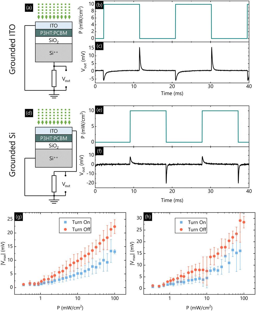 | ||
| Fig. 1 (a and d) Schematic diagram of photosensitive capacitor and circuit diagram of organic retinomorphic sensor (ORS) with (a) “Grounded ITO” connection, and (d) “Grounded Si” connection. (b and e) Example form of optical power density, P, incident on the photosensitive capacitor as a function of time. (c) Voltage across the resistor, Vout, for 1:1 blend (by wt%) of poly(3-hexylthiophene-2,5-diyl) (P3HT) to phenyl-C61-butyric acid methyl (PCBM) ORS as a function of time, in response to square wave P with grounded ITO configuration. (f) Vout as a function of time for 1:1 blend P3HT:PCBM ORS, in response to the square wave of P with grounded Si configuration. (g and h) Mean maximum magnitude of output voltage, |Vmax|, of three different ORSs with 1:1 blend of PCBM:P3HT, as a function of P with (g) grounded ITO configuration, and (h) grounded Si configuration. Error bars denote standard deviation between devices. R = 100 kΩ in all cases. Abbreviations: ITO: indium tin oxide, SiO2: silicon oxide, Si++: highly doped silicon. | ||
Fig. 1(b) shows an example of the time-dependence of optical power density, P, applied to photosensitive capacitor of our ORS. We use square wave illumination between 0 mW cm−2 and 10 mW cm−2 as it is the easiest waveform to interpret.23Fig. 1(c) shows the output voltage as a function of time for an ORS with a 1:1 (wt%) blend of P3HT:PCBM as the active layer, using the grounded ITO connection depicted in Fig. 1(a). The device exhibits a negative voltage spike in response to the light intensity increasing from 0 to 10 mW cm−2 (turn on) and a positive voltage spike in response to the light intensity decreasing from 10 mW cm−2 to 0 (turn off), consistent with previous results.15Fig. 1(g) shows the magnitude of the peak voltage height, |Vmax|, as a function of P for three identically-processed 1:1 blend P3HT:PCBM ORS devices, where points are the mean and the error bars are the standard deviation between the three devices.
An alternative way to connect the device is to connect the highly doped silicon to ground, essentially flipping the photosensitive capacitor connections, as shown in Fig. 1(d). We refer to this configuration as the “grounded Si” configuration. The same illumination waveform was applied to the photosensitive capacitor (Fig. 1(e)), but the resulting output voltage was observed to have a flipped sign relative to the grounded ITO configuration, as shown in Fig. 1(f). The dependence of |Vmax| on P was unchanged with the different connection, as shown in Fig. 1(h). The fact that signs are flipped with this connection is technologically relevant, as it now means the device will yield a positive voltage spike when the light intensity increases and a negative voltage spike when the light intensity decreases, which will likely be more intuitive for signal processing.11
These results also demonstrate that our previous description of the mechanism for ORSs is incomplete. Previously we claimed that under constant illumination, the overall net charge of the semiconductor became positive, resulting in charge being pulled onto the opposite plate of the capacitor (the Si++). However, this explanation is not consistent with the data in Fig. 1. According to our previous interpretation, when connected as shown in Fig. 1(d) there is a direct connection from the bottom electrode to ground with only the contact and cable resistance contributing to the RC time constant. Therefore, one would expect a much faster decay with this configuration, and one which was not tunable through a choice of R. This is inconsistent with experiment.
An alternative description is that the connection to ground is not hugely influential in this process, and instead charge equilibration occurs directly between the two electrodes. In this case, the excess charge produced in the semiconductor under illumination flows out across the ITO, through the resistor, and into the Si++ bottom electrode. A depiction of how this hypothesis could be tested is shown in Fig. 2(a). Here the two electrodes are connected together via a resistor, but neither are connected to ground. Essentially, the retinomorphic sensor is now the resistor and capacitor connected in parallel. The voltage is measured at the point between the capacitor and resistor, relative to ground. Because our oscilloscope has an input impedance of 1 MΩ, and the resistor between the terminals is 100 kΩ in all measurements here, only a small fraction of the current will flow to ground through the oscilloscope. In this case one would expect the resistor to influence the decay constant of the process both if Vout were defined between the Si terminal and ground (Fig. 2(a)) and between the ITO terminal and ground (Fig. 2(d)). Similarly, in this configuration switching the terminals would be expected to lead to a change in sign of voltage, consistent with the observations in Fig. 1.
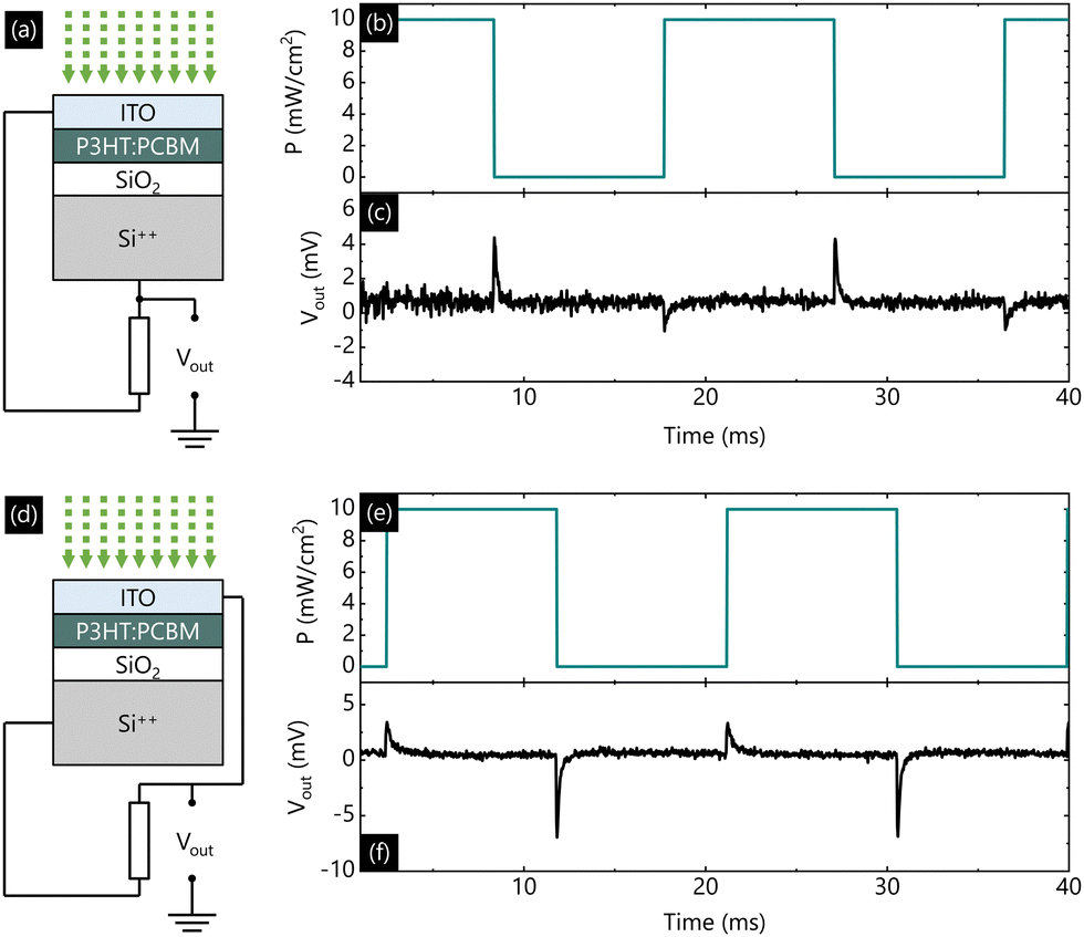 | ||
| Fig. 2 (a and d) Schematic diagrams of photosensitive capacitor and circuit diagram of organic retinomorphic sensor (ORS) with ITO and Si connected via a resistor, where (a) the output voltage, Vout, is defined at the Si contact and (d) Vout, is defined at the ITO contact. (b and e) Example form of optical power density, P, incident on the photosensitive capacitor as a function of time. (c) Voltage, Vout, defined between the Si terminal and ground for 1:1 blend (by wt%) of poly(3-hexylthiophene-2,5-diyl) (P3HT) to phenyl-C61-butyric acid methyl (PCBM) ORS as a function of time, in response to square wave P. (f) Voltage, Vout, defined between the ITO terminal and ground for 1:1 blend of P3HT:PCBM ORS as a function of time, in response to square wave P. R = 100 kΩ in all cases. Abbreviations: ITO: indium tin oxide, SiO2: silicon oxide, Si++: highly doped silicon. | ||
Measurements were carried out on ORSs in the configurations shown in Fig. 2(a and d), by applying a square wave of incident light between P = 0 and 10 mW cm−2, as shown in Fig. 2(b and e). As before, the output voltage was measured as a function of time in response to these waveforms. The resulting data shown in Fig. 2(c and f) is analogous to devices measured with the ground connection. This suggests that charge between the two plates is indeed more likely to equilibrate via the resistor, and not via ground as originally thought. The magnitude of Vout is lower in these configurations compared to those depicted in Fig. 1, suggesting that it is possible that re-equilibration of charge could be partially taking place via both the resistor and via ground. It is important to reiterate that device-to-device variation is large in these test devices, and that one must be careful drawing conclusions based on data from a single device alone. If some re-equilibration were occurring directly to ground in Fig. 1(a) for example, without going through the resistor, we would expect to see a very fast decay which could not be controlled by a choice of external resistor. This contradicts what is observed experimentally.
This is a result which we do not expect to significantly affect performance limits or behaviour, as the resistor would still define the decay constant of the device. However, if this description is accurate, it could conceivably make these devices more appealing from a process integration point-of-view because each pixel in an array would not need to be connected to ground. Instead, a single Vout terminal could be used for each pixel. To be consistent with experimental results, this description would also require there to be a net negative charge in the P3HT:PCBM layer under constant illumination, rather than a net positive charge as previously hypothesised.15 This is because in Fig. 2(a), for example, a net negative charge in the semiconductor layer would, through electrostatic repulsion, create a driving force that would act to push electrons out of the semiconductor towards the Si++. i.e., the Si++ terminal would be at a lower electrostatic potential than the ITO terminal immediately after illumination is applied. Since we are considering an electrostatic potential and not charge flow, the net excess of electrons do not need to be able to leave the semiconductor (and it is unlikely they will be able to, given the barrier height24) to induce a signal, they just need to be present. Since the voltage at both terminals is initially (in the dark) close to 0 V, the Si++ terminal must therefore be at a negative potential, and the ITO terminal at a positive potential, relative to ground, immediately after illumination is applied.
Another poorly understood aspect of ORSs is the origin of the net charge in the semiconductor. To operate as expected, an imbalance of charge is required in the semiconductor under constant illumination. This could occur via several different mechanisms. For example, though an asymmetry in monomolecular recombination rates of holes and electrons in the semiconductor, or an asymmetry of barrier heights for holes and electrons between the semiconductor and top electrode. However, it is generally expected that the responsible phenomenon should be more pronounced with more free charges generated overall. For this reason, we studied ORSs as a function of P3HT:PCBM blend ratio. It is hypothesized that changing the blend ratio should strongly influence the overall number of free charges (vs. bound excitons) generated in the bulk, which should in-turn affect the strength of the voltage output, regardless of specifics of the operation mechanism.
Fig. 3(a) shows the output voltage of 5 different ORSs with blend ratios of 100% P3HT, 1:2 P3HT:PCBM, 1:1 P3HT:PCBM, 2:1 P3HT:PCBM, and 100% PCBM (all by weight) for the absorber layer, in response to the light being turned on from 0 to 10 mW cm−2, with the grounded ITO configuration (as depicted in Fig. 1(a)). Fig. 3(b) shows equivalent data in response to the light being turned off from 10 to 0 mW cm−2. These measurements were carried out on 3 identically processed ORSs for each blend ratio. The mean values of |Vmax| were extracted for each device and plotted as a function of P3HT percentage in Fig. 3(c), where the error bars denote the standard deviation between the three devices. Fig. 3(d–f) show the equivalent data with the grounded Si configuration (as depicted in Fig. 1(d)).
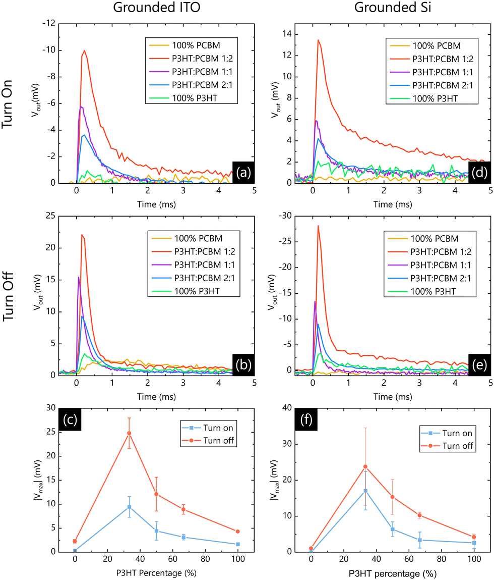 | ||
| Fig. 3 (a and b) Output voltage, Vout, of an organic retinomorphic sensors (ORSs) with various blends of poly(3-hexylthiophene-2,5-diyl) (P3HT) to phenyl-C61-butyric acid methyl (PCBM), measured as a function of time with the grounded ITO configuration, in response to (a) a step-change increase in optical power density, P, from 0 to 10 mW cm−2 (turn on) and (b) a step decrease in P from 10 mW cm−2 to 0 (turn off). (c) Mean maximum magnitude of output voltage, |Vmax|, as a function of the percentage of P3HT (by weight) in P3HT:PCBM ORSs with grounded ITO configuration, for three identically prepared devices. (d and e) Vout, of ORSs with various blend ratios of P3HT:PCBM measured as a function of time, with the grounded Si configuration, in response to (d) a step-change increase in optical power density, P, from 0 to 10 mW cm−2 (turn on) and (e) a step-change decrease in P from 10 mW cm−2 to 0 (turn off). (f) Mean |Vmax| as a function of the percentage of P3HT (by weight) in P3HT:PCBM ORSs with grounded Si configuration, for three identically prepared devices. The y-axis error bars in (c) and (f) represent the standard deviation between these three devices. | ||
The most notable feature of the data presented in Fig. 3 is that the signal is very low for the pure PCBM and pure P3HT devices, illustrating how both P3HT and PCBM are required for efficient device operation. This is consistent with optical spectroscopy studies into polymer:fullerene blends, where a finely intermixed blend of the two components is known to lead to efficient charge separation.25 This suggests that a larger concentration of free charges overall leads to a larger asymmetry in charge, and hence a larger signal. While not surprising, it is important to rule out the possibility that the signal was dominated by other processes, such as de-trapping at the semiconductor:dielectric interface. Here the strongest response to both the light turning on, and the light turning off is a 1:2 ratio of P3HT to PCBM, regardless of connection. This is in contrast to P3HT:PCBM organic photovoltaic (OPV) cells where a ratio close to 1:1 is generally found to yield best performance.26
The exact mechanism by which the proposed asymmetry in charge carriers is established is yet to be determined conclusively. However, a few plausible hypotheses exist. For example, it is well-known24 that the barrier between the highest occupied molecular orbital (HOMO) of P3HT and the work function of ITO is smaller than the barrier between the lowest unoccupied molecular orbital (LUMO) of PCBM and the work function of ITO. This suggests that holes will more readily diffuse out of the P3HT:PCBM into the ITO than electrons, under equal concentrations. Another possibility is that there exists an asymmetry in traps, either in the semiconductor or at the semiconductor:dielectric interface, which could lead to an asymmetry in trapped charge. As with many other aspects of this field, there remain many important experiments to be done in the future.
The thickness of the semiconductor absorption layer is another factor believed to affect the magnitude of the output signal.23 As the thickness of the active layer increases, the number of photons absorbed will increase and therefore more charges will be generated. This should hence yield a larger response for a given intensity. For this reason, we here studied the effect of absorption film thickness on the device performance via changing the spin-coating rotation speed, ω, to values of 800 rpm, 1500 rpm, and 4000 rpm. Fig. 4(a) shows |Vmax| as a function of P in response to the light turning on for these three spin-coating conditions. Fig. 4(b) shows equivalent data in response to the light turning off. All data presented in Fig. 4 were obtained with the grounded ITO configuration.
 | ||
| Fig. 4 Mean maximum output voltage, |Vmax|, of organic retinomorphic sensors (ORSs) with a 1:1 blend (by wt%) of poly(3-hexylthiophene-2,5-diyl) (P3HT) to phenyl-C61-butyric acid methyl (PCBM), as a function of optical power density, P, in response to (a) a step change increase in P from 0 to 10 mW cm−2 and (b) a step change decrease in P from 10 to 0 mW cm−2. P3HT:PCBM layers were deposited with deposition speeds of 4000 rpm, 1500 rpm, and 800 rpm. Error bars denote standard deviation between devices. All devices were measured with the grounded ITO configuration. | ||
All signals appear roughly comparable. Since film thickness is known to roughly be proportional to  when spin-coating,27 a larger voltage output for a lower ω is expected, but not observed. For this reason we suspect that microstructure also plays an important role in device performance here, as it does in OPVs.28 We acknowledge that using ω as a proxy for inverse film thickness is a crude strategy, and that standard deviations overlap in most cases. The use of vacuum deposited semiconductors would be a much more systematic way to study this, which can be achieved in future studies.
The lines in Fig. 4 are fits to a power law relationship between the magnitude of output voltage and the incident optical power density, given by eqn (1), where V0 is a prefactor and γ is a dimensionless exponent.
| Vmax = V0Pγ | (1) |
This equation is chosen based on our previous theoretical work on perovskite retinomorphic sensors,23 and other experimental studies into the relationship between photoconductivity and steady state illumination intensity, showing that charge density in most semiconductors obeys a power law relationship with incident optical power density.29 The exponent γ encapsulates the dominant recombination mechanism, with values close to ½ being indicative of bimolecular recombination.30 Because the experimental data does not follow a straight line on a log-log plot it is clear that a power law relationship is not an accurate description for all P. However, this is not unreasonable, given we can expect different recombination mechanisms in semiconductors to be dependent on carrier density.31 For this reason, we have fitted eqn (1) to the experimental data only when P is 1 mW cm−2 and above. Below this we assume bimolecular recombination to make a smaller contribution relative to monomolecular recombination. The extracted values of γ are shown in Table 1 in response to both the light turning on and to it turning off. All values are close to 0.5, suggesting that bimolecular recombination is indeed a dominant mechanism in all devices studied, at higher optical power densities.
| 4000 rpm | 1500 rpm | 800 rpm | |
|---|---|---|---|
| Turn on | 0.49 | 0.45 | 0.41 |
| Turn off | 0.48 | 0.41 | 0.48 |
Since long-term device predictability and reliability is a prerequisite for commercial viability, one of the most significant improvements in organic retinomorphic sensors over their perovskite counterparts14 is their stability under constant operation.15 The stability of our sensors was tested here by applying a square wave of light, and monitoring |Vmax| as a function of time. The measured |Vmax| of five compositions of the organic layer are shown in Fig. 5(a–e), all using the grounded ITO configuration. All the devices studied here exhibited excellent stability of over 12 hours under pulsed illumination.
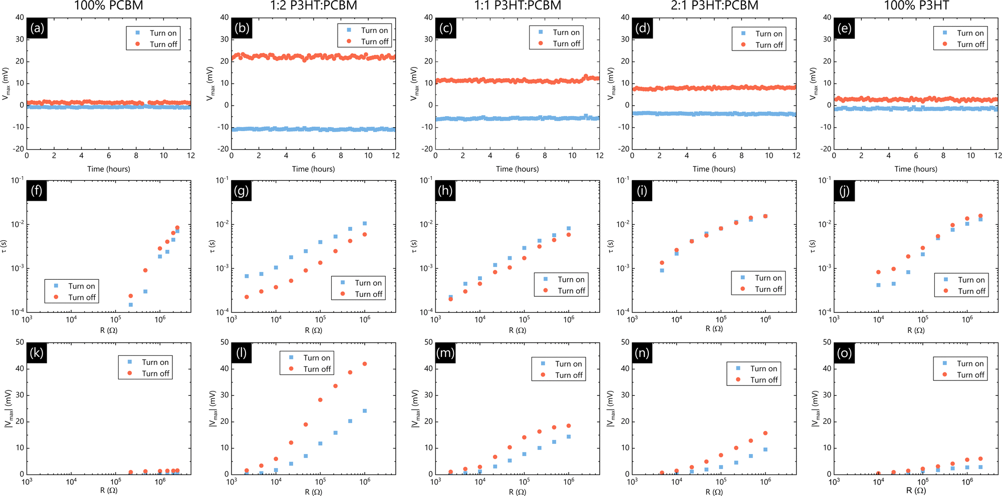 | ||
| Fig. 5 (a–e) Stability measurements of organic retinomorphic sensors (ORSs), where maximum output voltage, Vmax, is measured as a function of time under pulsed illumination from square wave of optical power density, P, between 0 and 10 mW cm−2, for (a) 100% PCBM, (b) 1:2 P3HT:PCBM, (c) 1:1 P3HT:PCBM, (d) 2:1 P3HT:PCBM, and (e) 100% P3HT, where P3HT is poly(3-hexylthiophene-2,5-diyl) (P3HT) and PCBM is phenyl-C61-butyric acid methyl PCBM, and ratios are by wt%. (f–j) Decay constant, τ, of ORS as a function of resistance, R, in response to light applied as step function from P = 0 to 10 mW cm−2 (“Turn On”) and from P = 10 to 0 mW cm−2 (“Turn Off”) for (f) 100% PCBM, (g) 1:2 P3HT:PCBM, (h) 1:1 P3HT:PCBM, (i) 2:1 P3HT:PCBM, and (j) 100% P3HT. All values were extracted assuming a monoexponential decay. (k–o) Magnitude of peak output voltage, |Vmax|, of ORS as a function of R, in response to light applied as step function from P = 0 to 10 mW cm−2 (“Turn On”) and from P = 10 to 0 mW cm−2 (“Turn Off”) for (k) 100% PCBM, (l) 1:2 P3HT:PCBM, (m) 1:1 P3HT:PCBM, (n) 2:1 P3HT:PCBM, and (o) 100% P3HT. For all stability measurements the period of the illumination waveform was 20 ms; 10 ms in the dark and 10 ms under illumination. | ||
The characteristic decay constant, τ, of an ORS is an important parameter as it defines the timescales over which past movement remains visible on such a sensor. With the resistor and capacitor as separate components of the ORS (as depicted in Fig. 1(a) for example), τ should be controllable through a choice of resistor R. Fig. 5(f–j) shows how τ varies as a function of R in response to turning the light on from P = 0 to 10 mW cm−2 and turning the light off from P = 10 to 0 mW cm−2. All measurements were carried out using the grounded ITO connection. As we have observed previously,15τ increases as R increases, which is as expected for an RC time constant. The fastest τ observed in this study was 220 μs in response to turning the light on, and 200 μs in response to turning the light off, which were obtained from the organic blend ratio of 1:1 P3HT:PCBM and a resistance of R = 2 kΩ. While a direct comparison with conventional cameras is not possible, values of τ = 200 μs imply objects which spend ≥200 μs in the visual field should be resolvable with such a sensor, roughly equivalent to a frame rate of 5000 frames per second.
In addition to a changing τ, the magnitude of the output voltage spike was also observed to decrease as the resistance decreased. This data is shown in Fig. 5(k–o). In our previous study we attributed this fall to a finite contact resistance in the device. With a constant contact resistance, one would expect the voltage dropped across it to increase as it became a larger percentage of the total resistance in the circuit.
Conclusions
In this report we have made several contributions to the understanding of organic retinomorphic sensors, and how they operate. The effects of connection configuration, the ratio of P3HT to PCBM in the absorption layer, and the thickness of semiconductor films, in blended polymer:fullerene organic retinomorphic sensors were studied. We identified a convenient way to switch the sign of the output voltage spike in response to an increase/decrease in light intensity, by reversing the device connections. We demonstrated how, much like organic solar cells, a mixture of two components (donor and acceptor) yield a much larger signal than when using a single component, all else being equal. Of the 5 compositions we considered, we found that a 1:2 blend ratio of P3HT to PCBM showed the highest signal intensity, while the pure P3HT and pure PCBM had the weakest signals. In addition, all the devices show excellent stability under constant illumination over 12 hours. The decay constants of these organic retinomorphic sensors were found to be tunable by changing the external resistor. As the resistance was decreased, both the decay constant and the magnitude of the output signal were also observed to decrease.
Together, this information represents a significant contribution to this field, which is still very much in its infancy. By providing examples of techniques to tune response, both in terms of signal intensity and decay constant, we have presented strategies which can be explored to improve these devices towards the future needs of industry. As more becomes known about these sensors, and as the field matures, it is hoped that they become more predictable, reliable, and ultimately, more commercially viable. Because these sensors represent a paradigm shift for optical sensing, there is much work that needs to be done, not only in terms of device design, but also readout, process integration, signal processing, and other topics. However, if successful, this new paradigm could potentially enable identification of objects which would have previously been impossible with conventional sensors.
Author contributions
Conceptualization: J. G. L.; methodology: X. Z. and J. G. L.; software: J. G. L.; validation: X. Z.; formal analysis: X. Z.; investigation: X. Z.; resources: J. G. L.; data curation: not applicable, writing – original draft: X.Z.; writing – review & editing: X. Z. and J. G. L.; visualization: X. Z. and J. G. L.; supervision: J. G. L.; project administration: J. G. L.; funding acquisition: J. G. L.Conflicts of interest
There are no conflicts to declare.Acknowledgements
The author thanks the National Science Foundation for financial support (Award number: 1942558). Part of this research was conducted at the Northwest Nanotechnology Infrastructure, a National Nanotechnology Coordinated Infrastructure site at Oregon State University which is supported in part by the National Science Foundation (Grant NNCI-2025489) and Oregon State University.Notes and references
- S. Yokogawa, I. Oshiyama, H. Ikeda, Y. Ebiko, T. Hirano, S. Saito, T. Oinoue, Y. Hagimoto and H. Iwamoto, Sci. Rep., 2017, 7, 3832 CrossRef PubMed.
- Y. Liu, Opt. Eng., 2016, 55, 016103 CrossRef.
- H. Chen, P. Li, X. Zheng, J. Sun and K. Li, eds. X. Hou, W. Zhao and B. Yao, Xi’an, China, 2007, p. 62795R.
- T. Hirayama, in 2013 IEEE Asian Solid-State Circuits Conference (A-SSCC), 2013, pp. 5–8.
- L. Gouveia and B. Choubey, Int. J. Smart Sens. Intell. Syst., 2020, 7, 1–6 Search PubMed.
- C. Posch, T. Serrano-Gotarredona, B. Linares-Barranco and T. Delbruck, Proc. IEEE, 2014, 102, 1470–1484 Search PubMed.
- F. Liao, F. Zhou and Y. Chai, J. Semicond., 2021, 42, 013105 CrossRef.
- G. Indiveri and R. Douglas, Science, 2000, 288, 1189–1190 CrossRef.
- J. Zhao, S. Ji, Z. Cai, Y. Zeng and Y. Wang, Biomimetics, 2022, 7, 31 CrossRef.
- P. Lichtsteiner, C. Posch and T. Delbruck, IEEE J. Solid-State Circuits, 2008, 43, 566–576 Search PubMed.
- G. Gallego, T. Delbrück, G. Orchard, C. Bartolozzi, B. Taba, A. Censi, S. Leutenegger, A. J. Davison, J. Conradt, K. Daniilidis and D. Scaramuzza, IEEE Trans. Pattern Anal. Mach. Intell., 2022, 44, 154–180 Search PubMed.
- D. K. Warland, P. Reinagel and M. Meister, J. Neurophysiol., 1997, 78, 2336–2350 CrossRef CAS PubMed.
- E. D. Adrian and R. Matthews, J. Physiol., 1927, 63, 378–414 CrossRef CAS PubMed.
- C. Trujillo Herrera and J. G. Labram, Appl. Phys. Lett., 2020, 117, 233501 CrossRef CAS.
- C. Trujillo Herrera and J. G. Labram, ACS Appl. Electron. Mater., 2022, 4, 92–98 CrossRef CAS.
- G. Yu, G. Srdanov, J. Wang, H. Wang, Y. Cao and A. J. Heeger, Synth. Met., 2000, 111–112, 133–137 CrossRef CAS.
- M. S. Vezie, S. Few, I. Meager, G. Pieridou, B. Dörling, R. S. Ashraf, A. R. Goñi, H. Bronstein, I. McCulloch, S. C. Hayes, M. Campoy-Quiles and J. Nelson, Nat. Mater., 2016, 15, 746–753 CrossRef CAS PubMed.
- A. Classen, C. L. Chochos, L. Lüer, V. G. Gregoriou, J. Wortmann, A. Osvet, K. Forberich, I. McCulloch, T. Heumüller and C. J. Brabec, Nat. Energy, 2020, 1–9 Search PubMed.
- A. Wadsworth, Z. Hamid, J. Kosco, N. Gasparini and I. McCulloch, Adv. Mater., 2020, 32, 2001763 CrossRef CAS PubMed.
- M. T. Dang, L. Hirsch and G. Wantz, Adv. Mater., 2011, 23, 3597–3602 CrossRef CAS.
- Y. Lin, M. I. Nugraha, Y. Firdaus, A. D. Scaccabarozzi, F. Aniés, A.-H. Emwas, E. Yengel, X. Zheng, J. Liu, W. Wahyudi, E. Yarali, H. Faber, O. M. Bakr, L. Tsetseris, M. Heeney and T. D. Anthopoulos, ACS Energy Lett., 2020, 5, 3663–3671 CrossRef CAS.
- L. Meng, Y. Zhang, X. Wan, C. Li, X. Zhang, Y. Wang, X. Ke, Z. Xiao, L. Ding, R. Xia, H.-L. Yip, Y. Cao and Y. Chen, Science, 2018, eaat2612 Search PubMed.
- C. T. Herrera and J. G. Labram, J. Phys. Appl. Phys., 2021, 54, 475110 CrossRef CAS.
- M. D. Irwin, D. B. Buchholz, A. W. Hains, R. P. H. Chang and T. J. Marks, Proc. Natl. Acad. Sci. U. S. A., 2008, 105, 2783–2787 CrossRef CAS.
- I.-W. Hwang, D. Moses and A. J. Heeger, J. Phys. Chem. C, 2008, 112, 4350–4354 CrossRef CAS.
- Y. Kim, S. A. Choulis, J. Nelson, D. D. C. Bradley, S. Cook and J. R. Durrant, J. Mater. Sci., 2005, 40, 1371–1376 CrossRef CAS.
- S. Wolf and R. N. Tauber, Silicon Processing for the VLSI Era: Process technology, Lattice Press, 2000 Search PubMed.
- C. J. Brabec, M. Heeney, I. McCulloch and J. Nelson, Chem. Soc. Rev., 2011, 40, 1185–1199 RSC.
- S. R. Cowan, A. Roy and A. J. Heeger, Phys. Rev. B: Condens. Matter Mater. Phys., 2010, 82, 245207 CrossRef.
- I. Balberg, J. Appl. Phys., 1994, 75, 914–923 CrossRef CAS.
- G. Lakhwani, A. Rao and R. H. Friend, Annu. Rev. Phys. Chem., 2014, 65, 557–581 CrossRef CAS PubMed.
| This journal is © The Royal Society of Chemistry 2022 |