
 Open Access Article
 This Open Access Article is licensed under a Creative Commons Attribution-Non Commercial 3.0 Unported Licence
Multimodal sensing in rewritable, data matrix azobenzene-based devices†
Alex
Boschi‡
 a,
Simone
Cinili‡
b,
Eva
Bystrenova
b,
Giampiero
Ruani
b,
Jessica
Groppi
ac,
Alberto
Credi
cd,
Massimo
Baroncini
*ce,
Andrea
Candini
*a,
Denis
Gentili
*b and
Massimiliano
Cavallini
*b
a,
Simone
Cinili‡
b,
Eva
Bystrenova
b,
Giampiero
Ruani
b,
Jessica
Groppi
ac,
Alberto
Credi
cd,
Massimo
Baroncini
*ce,
Andrea
Candini
*a,
Denis
Gentili
*b and
Massimiliano
Cavallini
*b
aIstituto per la Sintesi Organica e la Fotoreattività (ISOF), CNR. Via Gobetti 101, 40129 Bologna, Italy
bIstituto per lo Studio dei Materiali Nanostrutturati (ISMN), CNR. Via Gobetti 101, 40129 Bologna, Italy. E-mail: massimiliano.cavallini@cnr.it
cCLAN-Center for Light Activated Nanostructures, Istituto ISOF-CNR. Via Gobetti 101, 40129 Bologna, Italy
dDipartimento di Chimica Industriale “Toso Montanari”, Università di Bologna, Viale del Risorgimento 4, 40136 Bologna, Italy
eDipartimento di Scienze e Tecnologie Agro-alimentari, Università di Bologna, Viale Fanin 44, 40127 Bologna, Italy
First published on 22nd June 2022
Abstract
Here, we exploited the UV light and thermal triggered E ↔ Z photoisomerization of an azobenzene compound to fabricate multimodal readable and rewritable data matrix based devices. We first demonstrated that the UV light sensing capabilities can be simultaneously monitored by the change in optical, spectroscopic, and electrical properties. Then we exploited this capability by integrating tetra(azobenzene)methane crystals in a micrometric TAG whose information can be modified and repristinated by local UV treatment and thermal annealing. The system was characterized by polarized optical microscopy, Raman spectroscopy, conductive atomic force microscopy and Kelvin Probe Force Microscopy.
Introduction
Molecular switches are molecules capable of reversibly changing their chemical structure upon application of an external stimulus.1 They are attractive for basic science as well as for advanced technological applications, as their switching (i.e. the transition between two or more different molecular structures) upon exposure to an external stimulus usually results in drastic changes in specific optical, electrical, or chemical properties, thus enabling the possibility to control these characteristics on demand. Photochromic molecules are a class of switches in which the reversible interconversion between different molecular structures can be triggered by irradiation with light of an appropriate wavelength. They are widely employed in commercial products, such as industrial dyes2 and lenses,3 and are also investigated for application in data storage,4–6 to realize light-driven operations in molecular machines, smart materials7 and optoelectronic switches.8,9Among photochromic molecules, azobenzenes are particularly attractive and extensively studied due to their relatively straightforward synthesis, and highly efficient and fatigue resistant photo-isomerization.10 They are characterized by the presence of a nitrogen double bond around which a light induced E–Z isomerization can occur. Notably, the change in free volume associated with this process usually hinders solid state photoswitching, especially when azobenzene derivatives are grafted to a surface due to the loss of degrees of freedom and/or interaction with the substrate.11–13
Azobenzenes compounds, thanks to the versatility and multifunctional properties associated with their photoisomerization, offer an extraordinary opportunity for multi-modal sensing (i.e., the possibility to monitor more than one measurable physical parameter to detect changes in a system state).14 Here, we report on the solid-state multi-modal sensing capability of an azobenzene compound that, upon light-induced and thermal-restored transitions, can be monitored either optically or electrically. We exploited this feature by integrating the compound into a micrometric switchable and rewritable TAG with multiple read out methods. For our purposes we used a tetra(azobenzene)methane (1) molecule, (Fig. 1), whose synthesis and characterization are reported elsewhere.151 is a shape-persistent molecule composed of four azobenzene units covalently linked to a tetrahedral carbon atom. It presents a porous crystalline structure in its E configuration which is lost upon E → Z isomerization by UV light illumination. Most importantly, owing to the void space present in its crystalline structure, it is characterized by efficient E → Z photoswitching when exposed to UV light also in the solid state and in thin films.16,17
 | ||
| Fig. 1 Chemical structure of the investigated compound 1. | ||
Thin films of 1 were characterized optically by polarized optical microscopy (POM) and Raman spectroscopy and electrically by Kelvin Probe Force Microscopy (KPFM) and conductive AFM (Peak Force TUNA - PFTUNA).
Results and discussion
Thin deposits
Thin deposits of 1 were prepared starting from a CH3Cl solution by drop-casting in solvent saturated environments and at a controlled temperature on Si/SiO2 and Au/mica substrates for optical and electrical characterization studies, respectively (for details, see the Experimental section).When deposited, 1 has a strong tendency to form elongated crystals randomly distributed on the surface. Their width ranges from 10 μm to 50 μm resulting in an aspect ratio (length/width) between 1![[thin space (1/6-em)]](https://www.rsc.org/images/entities/char_2009.gif) :5 and >1:10. Under POM, the crystals exhibit a marked birefringence with a typical behavior of optically anisotropic materials. On rotating the polarizers, each crystal extinguishes the light at specific orientations, suggesting that each crystal is formed by domains oriented in the same direction. By drop casting a solution with a concentration of >5 g L−1 of 1 (indicative threshold, here indicated as high concentration), a randomly oriented distribution of contiguous crystals covering the entire surface is obtained (Fig. 2a), with an accumulation of the material at the boundaries of the droplet caused by the coffee stain effect.18 Under these conditions, the solution indeed reaches the supersaturation quickly and 1 starts to precipitate a few seconds after the deposition, i.e., when the solution still covers the entire surface of the sample, resulting, at the end of the process, in a continuous distribution of crystals. By drop casting a more diluted solution (<5 g L−1), 1 forms on the surface an irregular distribution of droplet-like structures with a diameter of a few microns. Each droplet-like structure is composed of an assembly of crystals. No material is observed in between the droplets (Fig. 2c) by POM or AFM. This difference in morphology is due to the fact that the liquid film of the diluted solution dewets on the surface before achieving supersaturation; the material is hence deposited in the final step of shrinking inside the former droplets.19
:5 and >1:10. Under POM, the crystals exhibit a marked birefringence with a typical behavior of optically anisotropic materials. On rotating the polarizers, each crystal extinguishes the light at specific orientations, suggesting that each crystal is formed by domains oriented in the same direction. By drop casting a solution with a concentration of >5 g L−1 of 1 (indicative threshold, here indicated as high concentration), a randomly oriented distribution of contiguous crystals covering the entire surface is obtained (Fig. 2a), with an accumulation of the material at the boundaries of the droplet caused by the coffee stain effect.18 Under these conditions, the solution indeed reaches the supersaturation quickly and 1 starts to precipitate a few seconds after the deposition, i.e., when the solution still covers the entire surface of the sample, resulting, at the end of the process, in a continuous distribution of crystals. By drop casting a more diluted solution (<5 g L−1), 1 forms on the surface an irregular distribution of droplet-like structures with a diameter of a few microns. Each droplet-like structure is composed of an assembly of crystals. No material is observed in between the droplets (Fig. 2c) by POM or AFM. This difference in morphology is due to the fact that the liquid film of the diluted solution dewets on the surface before achieving supersaturation; the material is hence deposited in the final step of shrinking inside the former droplets.19
 | ||
| Fig. 2 Optical micrographs of 1 drop-cast films and the effect of local UV treatment taken with cross polars. (a) Film obtained by drop casting a high concentration solution. (b) Effect of UV irradiation. (c) Film obtained by drop casting of a diluted solution. (d) Effect of UV irradiation. | ||
Importantly, the crystals formed inside the droplets exhibit the same characteristics as those observed in samples obtained by deposition of highly concentrated solutions. When exposed to UV light crystals of 1 show a complete loss of birefringence, a phenomenon related to the amorphization of the material induced by E → Z photoisomerization of its azobenzene units.14 Furthermore, we observed that a prolonged exposure to high intensity UV light induces a further alteration of the morphology of the crystals (Fig. 2b–d). Following a thermal treatment, the process can be reversed, and the crystalline status can be recovered.
Patterning
1 was patterned in nano- and micrometric structures by lithographically controlled wetting (LCW),20 a simple, fast and sustainable wet-patterning process widely used for patterning a large variety of functional materials.21–24 LCW enables large-area patterning of soluble materials, exploiting the capillary force of the menisci established under the protrusions of a stamp placed in contact with a liquid film and creating confinement conditions during solute precipitation.25 LCW is described in detailed in the Experimental section and ref. 19.1 was printed by LCW as a micrometric structure made of a square of 20 μm width and submicrometric parallel stripes with a controlled size (thus optically accessible).
Fig. 3 shows optical and AFM images of the printed structure. It is important to note that the printed micrometric structures exhibit the same morphology as that of the conventional thin deposit, i.e., each structure contains elongated, randomly distributed crystals, exhibiting a marked birefringence when observed by POM.
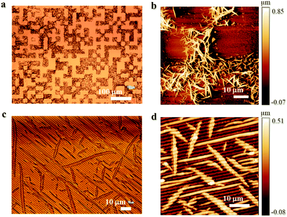 | ||
| Fig. 3 Micrometric and submicrometric structures of 1 fabricated by LCW on a silicon surface. (a) Optical micrographs of micrometric structures taken under bright field. (b) AFM topography of a. (c) Optical micrographs of sub-micrometric parallel stripes taken under bright field. (d) AFM topography of c. | ||
In the case of submicrometric stripes, on the other hand, the spatial confinement imposes the stamp's morphology on the crystalline growth, resulting in the formation of continuous parallel stripes with irregular thickness. In both cases AFM images show the presence of a continuous very thin film, ca. 1 nm thick in between the printed structures.
POM images show the typical behavior of optically anisotropic materials exhibiting birefringence: the printed stripes extinguish at the same orientations along their whole length in four positions at intervals of 90°. This evidence suggests that the crystalline domains are grown with the same orientation. Thus, we deduce that LCW has induced a coherent, long-range order along the direction of the stripes as often observed in artificial structures for a variety of functional materials patterned by LCW.
When treated with UV light, both types of samples exhibit the same behavior observed for drop-cast samples (Fig. 2c, d and 7). Noteworthy, no observable changes in morphology or POM images were observed even after ten cycles of UV treatments/thermal annealing (thus performing the transition from crystalline to amorphous and vice versa).
Multi-modal sensing
In Fig. 4 we report the topography and corresponding surface potential images of an area where a part of the 1 film has been illuminated with UV light for 60 minutes.
 | ||
| Fig. 4 AFM. (a) Topography and (b) surface potential of 1 thin submicrometric printed structures. The circle represents the area exposed to UV light for 60 min. (c) Zoomed images of pristine (E) and UV-exposed zones (Z). (d) Averaged cross-section profiles marked in the two surface potential images of (c). Different potential values can be assigned depending on the thickness and the isomerization state of the molecular film. | ||
The morphology of the two parts of the film, UV-exposed/pristine areas (respectively called Z/E, as we assume that most of the azobenzene units underwent photoisomerization after the prolonged irradiation time), evidences that the E → Z transformation is characterized also by a crystalline to amorphous transition, in agreement with the optical microscope measurements described in the previous section. A difference in the measured SP values is clearly observed. In addition, Fig. 4c shows detailed E/Z areas, where it is observed that multiple SP values can be further distinguished within the areas, corresponding to different film structures. In particular, inside the E areas we can distinguish different SP values for the thick film parts, the thin film parts, and the substrate, while inside the Z areas it is possible to discriminate the SP values for the thick and thin film parts. In the latter case, the thin film and substrate SP values cannot be distinguished, since the crystal to amorphous transition leads to a broadening of the film edge structures and a smearing of the KP measured signal. Nevertheless, it is possible to distinguish up to 5 distinct SP values.
Considering the above data, we concluded that the different E/Z phases of 1 can be directly detected by KPFM.
We further characterized the film by employing the PFTUNA module from Bruker, which allows the simultaneous probing of the sample morphology, along with its mechanical properties and electrical conductivity.29
Interestingly, we found significant differences between the measured adhesion values of the E and Z areas: more specifically, the illuminated (Z) areas show values 4–5 times higher than the non-illuminated (E) areas.
A change in the adhesion properties upon illumination has been already observed for other azobenzene-containing polymers.30 Our observation, along with the already reported possibility to detect a tunneling current from thin layers of tetra-azobenzene molecules,16 led us to investigate whether the electrical current can be used as a suitable additional read-out probe to distinguish between the E and Z areas. Intuitively, the different mechanical properties will result in different tip–sample interactions, from which we expect, by averaging many measurements, different resistance values. To this end, we measured more than 1000 I–V curves from two regions of 30 μm2 (we avoided consecutive measurements on the same spot since it leads to a mechanical breaking of the molecular film and I–V curves like the ones obtained on the gold substrate) in the E and Z areas, respectively, and averaged the results which are plotted in Fig. 5c. The shaded areas around the I–V curves correspond to the standard deviation as calculated for each bias value Vb. It is found that the conductivity of the Z zones is higher than the one of the E zones, which can be explained by considering that the amorphous regions can be more easily deformed by the tip, leading to, on average, shorter tip–sample distances, and hence higher current values, as schematically depicted in the inset. Our proof of principle result indicates that the optically induced switching can be read also electrically.
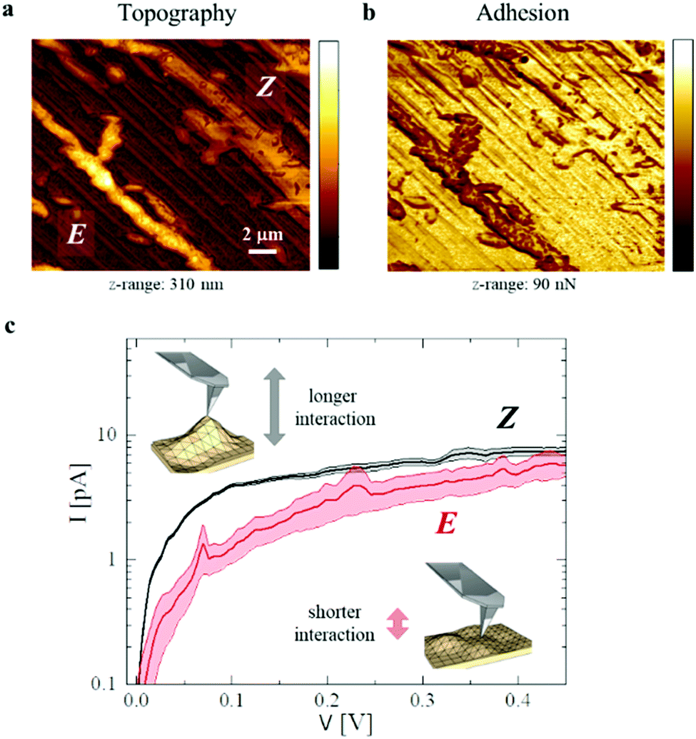 | ||
| Fig. 5 (a) Topography, (b) mechanical properties (adhesion), and (c) averaged current–voltage (I–V) plots of ∼1000 curves acquired on different areas. Shaded areas are the average standard deviations for each point. The two insets depict a scheme of the tip–film interaction during current measurements: the larger the film adhesion, the more the tip interacts with the film, leading to lower resistance value (i.e. higher current). | ||
As expected, the overall Raman spectrum remains mainly unaltered after UV treatment. However, after irradiation we observed a broadening of about 20% of almost all the peaks consistent with the amorphization of the system.
Moreover, a diagnostic peak at 1162.9 cm−1, corresponding to the CN stretch coupled with the ring breathing mode,32 redshifts at 1157.7 cm−1 and broadens more than three times as a consequence of the E → Z isomerization.
Fig. 6 shows the spectra of a crystal before and after UV treatment, corresponding to the two states, E and Z respectively. Despite the small intensity of the diagnostic peak Raman measures confirm the E–Z transition.
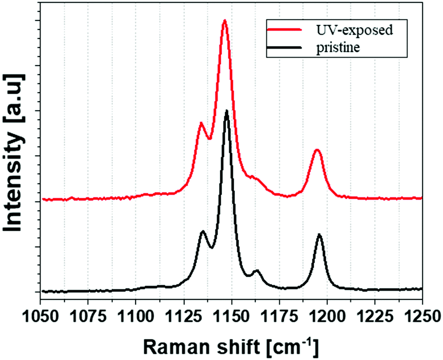 | ||
| Fig. 6 Raman spectra of thin deposits of 1, pristine (black line) and UV-exposed (red-line). The exciting laser has 632.8 nm wavelength. | ||
Considering the above data, we concluded that the different states of 1 can be directly detected by the birefringence, and/or surface potential, and/or electrical conductivity and/or Raman spectra.
Rewritable, data matrix devices
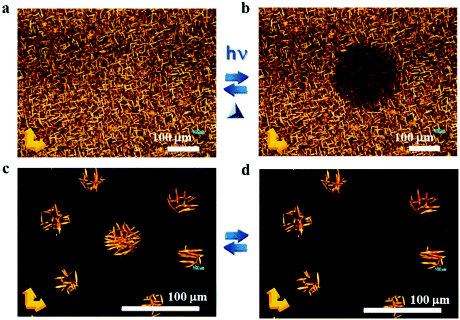
Inspired by the fact that the crystals of 1 turn off their birefringence upon UV light exposure, that can be read by multiple modes, we exploited the effect of switching to fabricate a multimodal readable, rewritable, data matrix device. In particular we fabricated a TAG reproducing a data-matrix Aztec code (i.e., a type of bidimensional digital code analogue to a QR code) made of modules of 20 μm in size. Fig. 7a shows an optical image of the TAG. | ||
| Fig. 7 Demonstration of modification and restoring of the information encoded in an Aztec data matrix made of 1 recorded by POM with modules of 20 μm size. (a) Large area optical image of the printed Aztec data matrix made of 1. (b) POM image of the portion of the TAG. (c) Modified information in the data matrix (black pixels). (d) Intermediated step of the restoring of information by thermal annealing. | ||
Fig. 7b shows a POM image of a portion of the TAG. We changed the information by switching off the birefringence of selected modules (Fig. 7c). The turning off was performed by selecting the desired modules using a fluorescence microscope and illuminating them for a few tens of seconds with UV light (for details, see the Experimental section). This operation corresponds to a change of the information contained in the TAG, as the deleted modules became dark when observed by POM. Importantly, a thermal annealing at 140 °C for one minute repristinates the original information in the TAG (Fig. 7c and d).
Here we show the POM images because they are the most representative and allow us to show an almost complete device. However, each module of the data matrix can be read by Raman, KPFM and PFTUNA, as described in the text.
Experimental section
Materials
Chloroform (anhydrous, 99.8%) was bought from Sigma Aldrich and used without further purification. Sylgard 184 (poly-dimethylsiloxane, PDMS) silicone elastomer base and the curing agent were purchased from Dow Corning.Thin deposits
Thin films of 1 were prepared by drop casting 10 μL of the solution in chloroform (1 g L−1 or 10 g L−1). The substrates consist of 10 × 10 mm2 pieces of silicon covered by 200 nm of thermal silicon oxides. For the electrical (KPFM and PFTUNA) characterization studies, a conductive substrate (evaporated gold on mica, Phasis, CH) was used in order to assure electrically connections with the thin deposits of 1.Patterning
Patterning of compound 1 was performed by lithographically controlled wetting (LCW), whose detailed protocol is reported in ref. 19. In LCW a mold made of PDMS is placed in contact with a thin film of solution spread on a substrate. The capillary forces pin the solution to the stamp protrusions leaving the other space free of solution. As the solution shrinks, it reaches supersaturation and the solute precipitates onto the substrate within the menisci, giving rise to a structured thin film, replicating the stamp protrusions. Fig. 8 shows a schematic representation of the LCW process. | ||
| Fig. 8 Scheme of lithographically controlled wetting (LCW). | ||
The PDMS stamps were prepared by replica molding of pre-patterned Si/SiO2 masters fabricated by photolithography. After curing for 6 h at 70 °C, the PDMS stamp was peeled off, cleaned by sonication in ethanol for 10 minutes, and dried in a stream of nitrogen prior to use. 10 μL cm−2 of a solution of 1 in chloroform (0.1–10 g L−1) at room temperature were drop-cast onto a substrate and a PDMS stamp was placed on the top. The solvent was allowed to evaporate at room temperature for 24 h. Afterwards, the stamp was removed, and, before characterization, the sample was aged under atmospheric conditions for 2 hours. Before the deposition, the substrates were cleaned by sonication in acetone, in 2-propanol, and then dried under a stream of nitrogen.
UV treatment
UV treatments were performed with a Nikon i-80 microscope equipped with epi-fluorescence (Hg lamp 100 W) using FM filters: Ex 400–440 (BP). The illumination was performed by a 100 W Hg lamp at a fixed power for 5 minutes for thin films and 1 minute for printed structures.Optical microscopy
Optical images were recorded with a Nikon i-80 microscope equipped with crossed polarizers. The images were recorded using a commercial CCD camera (Nikon CCD DS-2Mv).Raman spectroscopy
Raman spectra were recorded at room temperature in back-scattering geometry using a Renishaw 1000 micro-Raman, exciting at 632.8 nm and collecting the scattered light for 500 sec each. To avoid local heating of the crystals, the laser power was kept at 0.1 mW.Scanning probe microscopy (AFM, KPFM, PFTUNA)
Scanning probe microscopy characterization studies were performed in air with a Bruker Multimode 8 microscope. Kelvin probe force microscopy (KPFM) measurements were carried out in the amplitude modulated (AM) tapping mode. We also employed the Bruker's Peak-Force Tunneling Current Microscopy (PFTUNA) mode to measure simultaneously qualitative mechanical properties (i.e., adhesion) and the electrical current passing from the substrate to the tip through the sample. We used a Bruker “SCM-PIT-V2” probe (f = 75 kHz, k = 3 N m−1, material: n-Si) for AM-KPFM and a Bruker “PFTUNA” probe (f = 70 kHz, k = 0.4 N m−1, material: Pt–Ir coated Si3N4) for PFTUNA measurements. Scanning probe image processing for correcting piezo-scanner artifacts, as well as their analysis and I–V curves analysis, was performed with SPIP software.Conclusions
To conclude, we reported on the characterization and application in rewritable data matrix devices of an azobenzene based molecular photoswitch. We proved that compound 1 can be used as a material for optical information storage with a multi-modal response. In particular, we showed that the optical switching of 1 exhibits a simultaneous change of birefringence, electrical conductivity and Raman spectra, which we exploited in a multi-modal and rewritable data matrix device, demonstrating the direct application of azobenzene compounds in advanced TAG. Furthermore, it is possible to distinguish up to 5 distinct surface potential values showing the potentiality to use a patterned tetra-azobenzene film as an active layer for the development of molecular memories with multiple data levels. In addition, the progressive recovery of birefringence upon thermal treatment potentially allows azobenzene to be used for less conventional applications, such as temperature integrators, i.e., devices capable to record the thermal history.33,34While the degree of switching of electrical conductivity and diagnostic Raman peaks need to be further optimized to realize devices suitable for application, the existing literature on azobenzene compounds makes us confident that a similar approach can be further extended to similar materials, enabling new applicative perspectives for this important class of materials.
Conflicts of interest
There are no conflicts to declare.Acknowledgements
We are grateful for the financial support provided by the Italian Ministry of Education, University and Research. National project PRIN “Next generation of molecular and supramolecular machines: towards functional nanostructured devices, interfaces, surfaces and materials (NEMO)” Prot. 20173L7W8K.Notes and references
- J. P. Sauvage and V. Amendola, Molecular Machines and Motors, Springer Science & Business Media, 2001, vol. 99 Search PubMed.
- S. Nigel Corns, S. M. Partington and A. D. Towns, Color. Tech., 2009, 125, 249–261 CrossRef.
- B. van Gemert, Mol. Cryst. Liq. Cryst. Sci. Technol., Sect. A, 2000, 344, 57–62 CrossRef CAS.
- C. C. Corredor, Z.-L. Huang, K. D. Belfield, A. R. Morales and M. V. Bondar, Chem. Mat., 2007, 19, 5165–5173 CrossRef CAS.
- V. Adam, H. Mizuno, A. Grichine, J. Hotta, Y. Yamagata, B. Moeyaert, G. U. Nienhaus, A. Miyawaki, D. Bourgeois and J. Hofkens, J. Biotech., 2010, 149, 289–298 CrossRef CAS PubMed.
- S. Venkataramani, U. Jana, M. Dommaschk, F. D. Sönnichsen, F. Tuczek and R. Herges, Science, 2011, 331, 445–448 CrossRef CAS PubMed.
- V. Balzani, A. Credi and M. Venturi, Chem. Soc. Rev., 2009, 38, 1542–1550 RSC.
- J. M. Mativetsky, G. Pace, M. Elbing, M. A. Rampi, M. Mayor and P. Samori, J. Am. Chem. Soc., 2008, 130, 9192–9193 CrossRef CAS PubMed.
- C. Raimondo, N. Crivillers, F. Reinders, F. Sander, M. Mayor and P. Samorì, Proc. Natl. Acad. Sci. U. S. A., 2012, 109, 12375–12380 CrossRef CAS PubMed.
- H. M. D. Bandara and S. C. Burdette, Chem. Soc. Rev., 2012, 41, 1809–1825 RSC.
- R. A. Evans, T. L. Hanley, M. A. Skidmore, T. P. Davis, G. K. Such, L. H. Yee, G. E. Ball and D. A. Lewis, Nat. Mat., 2005, 4, 249–253 CrossRef CAS PubMed.
- P. Tegeder, J. Phys.: Condens. Matter, 2012, 24, 394001 CrossRef PubMed.
- C. Dri, M. v Peters, J. Schwarz, S. Hecht and L. Grill, Nat. Nanotechnol., 2008, 3, 649–653 CrossRef CAS PubMed.
- D. Gentili, et al., Multi-modal sensing in spin crossover compounds, J. Mat. Chem. C, 2015, 3, 7836–7844 RSC.
- M. Baroncini, S. d’Agostino, G. Bergamini, P. Ceroni, A. Comotti, P. Sozzani, I. Bassanetti, F. Grepioni, T. M. Hernandez, S. Silvi, M. Venturi and A. Credi, Nat. Chem., 2015, 7, 634–640 CrossRef CAS PubMed.
- C. Nacci, M. Baroncini, A. Credi and L. Grill, Angew. Chem., Int. Ed., 2018, 57, 15034–15039 CrossRef CAS PubMed.
- D. Takamatsu, K. Fukui, S. Aroua and Y. Yamakoshi, Org. Biomol. Chem., 2010, 8, 3655–3664 RSC.
- R. D. Deegan, O. Bakajin, T. F. Dupont, G. Huber, S. R. Nagel and T. A. Witten, Nature, 1997, 389, 827–829 CrossRef CAS.
- M. Cavallini, D. Gentili, P. Greco, F. Valle and F. Biscarini, Nat. Protoc., 2012, 7, 1668–1676 CrossRef CAS PubMed.
- M. Cavallini, J. Mater. Chem., 2009, 19, 6085–6092 RSC.
- M. Melucci, M. Zambianchi, L. Favaretto, V. Palermo, E. Treossi, M. Montalti, S. Bonacchi and M. Cavallini, Chem. Commun., 2011, 47, 1689–1691 RSC.
- M. Cavallini, I. Bergenti, S. Milita, J. C. Kengne, D. Gentili, G. Ruani, I. Salitros, V. Meded and M. Ruben, Langmuir, 2011, 27, 4076–4081 CrossRef CAS PubMed.
- M. Cavallini, Z. Hemmatian, A. Riminucci, M. Prezioso, V. Morandi and M. Murgia, Adv. Mat., 2012, 24, 1197–1201 CrossRef CAS PubMed.
- D. Gentili, P. D’Angelo, F. Militano, R. Mazzei, T. Poerio, M. Brucale, G. Tarabella, S. Bonetti, S. L. Marasso and M. Cocuzza, J. Mat. Chem. B, 2018, 6, 5400–5406 RSC.
- D. Gentili, F. Valle, C. Albonetti, F. Liscio and M. Cavallini, Acc. Chem. Res., 2014, 47, 2692–2699 CrossRef CAS PubMed.
- D. J. W. Bullock, C. W. N. Cumper and A. I. Vogel, J. Chem. Soc., 1965, 5316–5323 RSC.
- V. Quintano, V. Diez-Cabanes, S. Dell’Elce, L. di Mario, S. P. Cresi, A. Paladini, D. Beljonne, A. Liscio and V. Palermo, Phys. Chem. Chem. Phys., 2021, 23, 11698–11708 RSC.
- N. Crivillers, A. Liscio, F. di Stasio, C. van Dyck, S. Osella, D. Cornil, S. Mian, G. M. Lazzerini, O. Fenwick, E. Orgiu, F. Reinders, S. Braun, M. Fahlman, M. Mayor, J. Cornil, V. Palermo, F. Cacialli and P. Samorì, Phys. Chem. Chem. Phys., 2011, 13, 14302–14310 RSC.
- https://www.bruker.com/en/products-and-solutions/microscopes/materials-afm/afm-modes/pf-tuna.html .
- H. Zhou, C. Xue, P. Weis, Y. Suzuki, S. Huang, K. Koynov, G. K. Auernhammer, R. Berger, H.-J. Butt and S. Wu, Nat. Chem., 2017, 9, 145–151 CrossRef CAS PubMed.
- C. M. Stuart, R. R. Frontiera and R. A. Mathies, J. Phys. Chem. A, 2007, 111, 12072–12080 CrossRef CAS PubMed.
- Y. B. Zheng, J. L. Payton, C.-H. Chung, R. Liu, S. Cheunkar, B. K. Pathem, Y. Yang, L. Jensen and P. S. Weiss, Nano Lett., 2011, 11, 3447–3452 CrossRef CAS PubMed.
- M. Cavallini, A. Calò, P. Stoliar, J. C. Kengne, S. Martins, F. C. Matacotta, F. Quist, G. Gbabode, N. Dumont and Y. H. Geerts, Adv. Mat., 2009, 21, 4688–4691 CrossRef CAS.
- M. Cavallini and M. Melucci, ACS Appl. Mater. Interfaces, 2015, 7, 16897–16906 CrossRef CAS PubMed.
Footnotes |
| † Electronic supplementary information (ESI) available. See DOI: https://doi.org/10.1039/d2tc01565j |
| ‡ AB and SC contributed equally to the work. |
| This journal is © The Royal Society of Chemistry 2022 |