Emerging polymer electrets for transistor-structured memory devices and artificial synapses

Ting-Wei Chang a, Yun-Shan Li a, Naoji Matsuhisa bc and Chien-Chung Shih *a
aDepartment of Chemical Engineering and Materials Engineering, National Yunlin University of Science and Technology, Yunlin 64002, Taiwan. E-mail: shihcc@yuntech.edu.tw
bElectronics and Electrical Engineering, Faculty of Science and Engineering, Keio University, Yokohama 223-8522, Japan
cInstitute of Industrial Science, The University of Tokyo, 4-6-1, Komaba, Tokyo 153-8505, Meguro-ku, Japan

Received 20th March 2022 , Accepted 20th May 2022

First published on 30th May 2022


Abstract

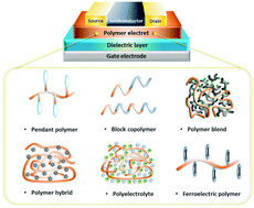
Polymer electrets have been widely explored as charge-storage elements in field-effect transistor memory and artificial synaptic devices because of their tailorable molecular structures and processability. Proper design of polymer electrets can enhance the charge injection efficiency and storage time, and the memory implementation can be switched from electrical to optical programming. We comprehensively review state-of-the-art polymer electrets for transistor-structured memory and artificial synapses. We classify the electrets into five types: (1) pendant polymer electrets, (2) block copolymer electrets, (3) conjugated polymer electrets, (4) hybrid polymer composites, and (5) ferroelectric polymer electrets. Their design concepts and working mechanisms are discussed in detail. This review may pave the way for the development of polymer-electret-based transistor memory devices and artificial synapses with unprecedented performance improvements.


image file: d2tc01132h-p1.tif

Ting-Wei Chang

Ting-Wei Chang received his bachelor's degree in the Department of Chemical and Materials Engineering from National Yunlin University of Science and Technology (NYUST) in 2020. He then joined Dr Chien-Chung Shih's group for master program in 2021. His research focuses on the synthesis of conjugated polymers and their applications on organic field-effect transistors and memory devices.

image file: d2tc01132h-p2.tif

Yun-Shan Li

Yun-Shan Li is currently an undergraduate student in the Department of Chemical and Materials Engineering, National Yunlin University of Science and Technology (NYUST). She joined Dr Chien-Chung Shih's lab in the summer of 2021 for research. Her research focuses on stretchable and patternable micro-supercapacitors.

image file: d2tc01132h-p3.tif

Naoji Matsuhisa

Dr Naoji Matsuhisa received his PhD degree from the Department of Electrical Engineering and Information Systems in the University of Tokyo in 2017. After his studies, he then worked as a postdoc in the Department of Materials Science and Engineering at Nanyang Technological University in Singapore, and the Department of Chemical Engineering at Stanford University in the U.S. In April 2020, he joined to the Department of Electronics and Electrical Engineering at Keio University as an Assistant Professor. In April 2022, he became an Associate Professor in Institute of Industrial Science at the University of Tokyo. He has developed stretchable electronic materials and the devices.

image file: d2tc01132h-p4.tif

Chien-Chung Shih

Dr Chien-Chung Shih is an Assistant Professor of Chemical and Materials Engineering at National Yunlin University of Science and Technology (NYUST). He received his PhD degree in Chemical Engineering from National Taiwan University in 2016 and joined Prof. Wen-Chang Chen's group as a postdoc researcher from 2016–2019. Prior to joining faculty, he conducted his postdoc research and worked with Prof. Zhenan Bao at Stanford University from 2019 to 2021. His research focuses on conjugated polymers and their applications in field-effect transistors, transistor-structured memory, phototransistors and sorting of single-walled carbon nanotubes.


1. Introduction

Nonvolatile memory devices are widely used in applications such as displays, cellular phones, and computer systems.1–8 These devices carry necessary data for the operation of modern electronics. With the development of lightweight, portable, and wearable electronics, the demand for flexible memory devices in integrated circuits has increased. For instance, diverse healthcare applications based on wearable devices are emerging. In particular, imperceptible sensor-laden devices with sophisticated layouts have been designed to continuously measure physiological parameters and coupled with data storage devices for advanced applications in personal healthcare.9–12 In this case, high-performance local memory is required to store the buffer of feedback signals from the body in real time. Accordingly, interest has increased in organic memory devices owing to their intrinsic flexibility and solution processability on flexible and stretchable substrates with adjustable patterns for circuit integration. An objective of next-generation nonvolatile memory devices is achieving ultrahigh-density storage to match the rapid development of the Internet of Things and the urgent demand for information storage in big data technologies. Nevertheless, real-world data generation outpaces storage capacity in digital technologies.13,14

The continuous data exchange between a processor and memory device produces substantial delays and limits the computing speed and energy efficiency, in an effect commonly known as the von Neumann bottleneck.15,16 Hence, advanced nonvolatile memory technologies are required to construct parallel and reconfigurable neural networks that can simultaneously process and store information, resembling the function of the human brain. The human brain is composed of approximately 1011 basic units called neurons, which are connected by approximately 1015 links called synapses.17 The transmission and processing of voltage pulse signals by synapses is the basis for cognitive and learning functions in the brain. Hardware implementation of synapses and neurons using emerging electronic devices is promising for brain-inspired computing. Moreover, the development of an electronic device with synaptic functions is essential for constructing neuromorphic computing systems.18

Synaptic transistors, which are transistor-structured memory devices with medium volatility, can emulate synapses.19–22 Depending on their volatility, there are long and short-term memory devices. A synaptic transistor has long-term memory because it exhibits medium volatility and hysteresis under excitation of an external electric field for programming. The gate electrode in the transistor is generally considered as the preterminal that applies action potentials to the synapse, and the active channel that contacts the source/drain electrodes is considered as the post-stimulus. Then, the control of the channel by a presynaptic gate allows signal transmission and transient storage. A synaptic transistor can exhibit multilevel accessible conductance states by regulating multiple presynaptic inputs to obtain an analog-type response. Extensive research has been devoted to developing synaptic transistors with high density, fast operation, low voltage, and operational reliability. In addition, applications such as electronic skins and implantable electronics require flexible synaptic transistors that are nontoxic, harmless, and biocompatible.23–25

Over the past two decades, new materials and device architectures have been proposed to address problems in organic memory devices. The device architecture mainly comprises a two-terminal resistive memory and three-terminal transistor memory.8,26 A typical resistive memory device generally consists of two electrodes enclosing a switching layer for toggling between high and low resistances in response to an external voltage. Although resistive memory can provide high storage capacity, fast speed, short access time, and low power consumption, signal transmission and programming cannot be performed collectively, restricting its applicability for artificial synapses owing to the interfering learning and forgetting functions. On the other hand, three-terminal transistor memory, such as organic field-effect transistor (OFET) memory, can receive and read stimuli concurrently while showing similar advantages to resistive memory, being promising for integrated neuromorphic systems. This type of memory is considered as a new generation of portable high-density storage device owing to its flexibility, light weight, and compatibility with complementary logic circuits.13

OFET memory can be classified into three categories according to the charge-storage mechanism of the memory layer: (1) floating-gate OFET memory,27,28 (2) polymer-electret-based OFET memory,29,30 and (3) ferroelectric OFET memory.31 Polymer electrets possess unique advantages, such as high mechanical strength, high flexibility, and processability.3 Thus, polymer-electret-based OFET memory devices are compatible for fabrication by solution processes including spin coating, dip coating, spray coating, and inkjet printing without requiring vacuum deposition. A polymer electret can temporarily capture electrons or holes to hold a quasi-permanent electric field under external bias. Even if the voltage of the gate electrode is removed, the change in conductance can be retained to some extent, resulting in bidirectional shifts in the threshold voltage. Compared with ferroelectric and floating-gate transistor memory, electret-based transistor memory shows higher writing and erasing speed, higher on/off current ratio, larger memory window, and higher stability.32 Furthermore, polymer electrets provide transistors with extensible sensory functionalities such as tactile memory and photonic memory by their tunable molecular structure. For example, multistate photonic transistor memory has been achieved using conjugated polymer electrets to form the dielectric layer. Then, the channel conductance of the transistor can be gradually controlled via photogenerated electrons from the electret and is preserved after removing light.33,34 Moreover, multilevel storage in the transistor can enhance capacity, reduce memory space, and emulate synapses for brain-inspired computing.35,36 Therefore, numerous studies have been focused on exploiting memory characteristics and photonic synaptic behaviors.37

In this review, we analyze representative polymer electrets and their composites for OFET memory devices and correlate chemical structures, morphology, charge transport, and memory characteristics. We begin by providing a brief introduction of the working mechanisms of transistor memory and neuromorphic transistors. Next, research progress of transistor memory devices using various polymers as charge storage layers, including pendant polymer electrets, block copolymer electrets, conjugated polymer electrets, ferroelectric polymer electrets, and hybrid nanocomposite electrets is summarized (Fig. 1a). Recent developments in artificial synapses constructed on OFET memory devices based on polymer electrets are then highlighted. Finally, we outline the challenges and outlook for future developments on organic transistor memory devices.


image file: d2tc01132h-f1.tif
Fig. 1 (a) Schematic illustrations of the transistor memory based on polymer electrets with a bottom-gate top-contact configuration. (b) Ids1/2vs. Vgs curve under applied voltage bias that can determine the memory window and memory ratio. (c) Retention time test and (d) endurance cycles on OFET memory devices.

2. Working principles of memory

2.1 OFET memory

An OFET can have a top or bottom gate and top or bottom contact according to the relative contact position of the active layer and source/drain electrodes. Basically, the OFET is characterized by the drain–source current (Ids) according to the gate–source voltage (Vgs) and Ids according to the drain–source voltage (Vds), which form the transfer and output curves, respectively. Current Ids on both logarithmic and linear scales according to voltage Vgs can be depicted by transfer characteristics to extract important performance parameters. Current Ids in the saturation region can be obtained from the transfer curves as follows:
image file: d2tc01132h-t1.tif
where W and L represent the width and length of the channel region, respectively, μ and Ci are the mobility and capacitance per unit area of dielectric film, respectively, and Vth is the threshold voltage. In the curve of Ids1/2 according to Vgs, the slope is linearly proportional to the square root of mobility. Thus, when a sufficient Vgs is applied, the charge-capture layer develops a stable built-in electric field that stores charge carriers and produces hysteresis, establishing operation program. This state can be eliminated by applying a reverse gate bias, establishing operation erase (Fig. 1b). Current Ids in the programmed and erased states represent 1 and 0, respectively.

Several parameters are used to determine the OFET memory characteristics, including the memory window, memory ratio, retention, and endurance ability. The Vth shift between the programmed and erased states is defined as the memory window, which is one of the most important parameters in OFET memory for distinguishing the information storage level. The retention measures the ability of a memory device to preserve the programmed and erased states without losing the trapped charges through the leakage path over time (Fig. 1c). Commercial OFET memory devices are expected to maintain reliability over 10 years at room temperature, while current studies show results on the order of 103 to 106 s.4 The memory endurance can be evaluated by repeated program/erase cycles (Fig. 1d). The ideal endurance is over 106 cycles for nonvolatile secondary storage. However, the typical endurance results for OFET memory are range in 102–105 cycles.2

2.2 Biological synapses and synaptic transistors

A synaptic transistor is a three-terminal device with a structure similar to that of a transistor-structured memory.38,39 In a synaptic transistor, operation program is on the gate and decoupled from the operation read on the channel, enabling the synaptic transistor to simultaneously execute learning functions and signal transmission. The physically separated configuration of terminals endows synaptic transistor memory with low nonlinearity and variability, being suitable for fast and accurate training of artificial neural networks. As shown in Fig. 2a, the gate and source/drain are commonly used as the presynaptic and postsynaptic terminals, respectively. To simulate the behavior of biological synapses, voltage pulses are applied to the gate electrode, resembling presynaptic spikes on the presynaptic membrane. The mobile charges in the channel are regarded as neurotransmitters (Fig. 2b).19 Channel conductance is regarded as the synaptic weight (W), whose changes are known as synaptic plasticity. In neurology, synaptic plasticity depends on the activity on either or both sides of a synapse. Generally, synaptic plasticity is divided into short- and long-term plasticity. Short-term plasticity corresponds to a transient modification in the synaptic strength after stimulation, lasting from tens of milliseconds to a few minutes, whereas long-term plasticity is a persistent modification in the synaptic strength, lasting from hours to years. Short-term plasticity is required for transmission, encoding, and filtering of neural signals, whereas long-term plasticity establishes more permanent changes in the neural loop to contribute to memory and learning.40 In addition, there are two forms of synaptic responses, namely, potentiation (excitatory postsynaptic current – EPSC) and depression (inhibitory postsynaptic current – IPSC), which are linked to the strengthening and weakening of the synaptic weight, respectively. The abovementioned synaptic functions form the foundation for implementing bioinspired models of neural processing.41
image file: d2tc01132h-f2.tif
Fig. 2 (a) Schematic demonstration of biological neuron and synapse structure. (b) Schematic diagram of the synaptic OFET memory devices.

The operation of synaptic transistors can be divided into two types according to the source of stimulation. For electrical stimulation, based on transistor-structured memory, charges can tunnel from the semiconductor channel to the charge-trapping site under an applied gate voltage, and the captured charges in the floating gate or interface induce control of the channel conductance. For light stimulation, upon exposure to light, excitons are generated, separated, and finally captured in the charge-trapping sites or interface defects, modulating the channel conductance. By engineering the trapping levels in terms of the interfacial effect and/or bulk trapping, synaptic transistors can be operated in volatile or nonvolatile modes according to the amplitude, frequency, and number of gate inputs, ensuring short- and long-term plasticity within a single memory cell. Synaptic transistors may lead to new paradigms to address complicated artificial intelligence problems, such as pattern recognition and classification, bipedal locomotion control, and decision-making.

3. Development of polymer electrets for transistor-structured memory devices

A polymer electret is a dielectric material that can acquire a quasi-permanent electrical charge. A polymer electret below the channel provides field-assisted transfer of charges from the channel to the polymer and localization of these charges by deep traps in the polymer. The resulting immobilization of the transferred charge by deep traps in the polymer produces a Vth shift, which can enhance charge storage of a memory device. The storage of charges in polymer electrets can be explained by the orientation of permanent dipoles and charge trapping by structural defects or boundaries. The characterization of charge-trapping materials in polymer electrets involves surface properties, dielectric properties, and molecular structure properties.3 In a polymer electret-based system, because the transport of charge carriers occurs in the first few monolayers of organic semiconductors adjacent to the interface of the gate dielectrics, the morphology of the charge-trapping layer affects the growth of the deposited semiconductor thin films regarding aspects such as crystallinity, grain size, grain boundaries, and packing orientation, which in turn influence the transport and retention of trapped charges.

Several approaches can be used to achieve memory characteristics in transistors using polymeric materials, which can be divided into (1) pendant polymer electrets, (2) block copolymer electrets, (3) conjugated polymer electrets, (4) hybrid polymer composites, and (5) ferroelectric polymer electrets. In this section, we analyze the advantages and disadvantages of different systems based on polymer electrets. Tables 1 and 2 summarizes the OFET memory characteristics of representative polymer electrets and their nanocomposite, respectively. Small molecules are preferred for the use as channel materials because they can be processed in vacuum deposition, and this prevents the damage of the polymer electrets from the solvent during spin-coating of polymer semiconductor solution.

Table 1 Summary of OFET memory performances based on polymer electrets
Electret Channel Operation modea ΔVthb I on/Ioffc Retention Ref.
a EW: electrical writing; PW: photowriting; EE: electrical erasing; PE: photoerasing; pEW: photoassisted electrical writing; pEE: photoassisted electrical erasing. b ΔVth: memory window. c I on/Ioff: memory ratio.
Pendant polymer PαMS Pentacene EW EE (±70 V) 26 105 >105 s 29
PS Pentacene EW EE (±70 V) 22 105 >105 s 29
PVN Pentacene EW EE (±70 V) 27 106 >105 s 29
PVN PDVT-10 EW EE (±40 V) 37 106 43
P(St-co-Pys) Pentacene EW EE (±100 V) 41 105 >104 s 44
FPS C12-BTBT EW EE (±100 V) 76 106 >104 s 45
P(St-Fl) BPE-PTCDI EW EE (±100 V) 81 103 >105 s 46
PVTT BPE-PTCDI EW EE (±100 V) 43 102 >105 s 46
Block copolymer MH-b-PS Pentacene EW EE (±50 V) 26 108 >104 s 47
MH-b-PStFln Pentacene EW EE (±50 V) 37 108 >104 s 48
PS-b-P4VP(FM) Pentacene EW EE (±100 V) 46 107 >105 s 49
P3HT44-b-Pison EW EE (±100 V) 62 105 >104 s 50
Sol-PDI Pentacene PW (640 nm) EE (60 V) 7 105 >104 s 51
Conjugated polymer PFO NPs Pentacene EW EE (±50 V) 21 106 >104 s 52
poly(PEGMA)m-b-poly(DB3VT)n Pentacene EW EE (±50 V) 34 105 >104 s 53
β-PFO Pentacene EW (−80 V) PE (white) 57 103 >104 s 54
PFO/PS blend Pentacene PW (405 nm) EE (−30 V) 21 106 >104 s 34
F8BT/PMMA C10-DNTT PW (455 nm) EE (−60 V) 14 103 >104 s 55
PFO5k-b-PS22k Pentacene PW (405 nm) EE (−40 V) 21 104 >104 s 33
PFO-b-POXD BPE-PDI EW (−60 V) PE (254 nm) 20 105 >104 s 56
PF-b-Piso Pentacene PW (405 nm) EE (−40 V) 33 106 >104 s 57
TPA-CN-TPE Pentacene pEW pEE (±100 V) (365 nm) 42 104 >104 s 58
Poly(CD) Pentacene EW (−90 V) PE (white) 82 103 >104 s 59


Table 2 OFET memory device performance based on polymer hybrid nanocomposite
Electret Channel Operation modea ΔVthb I on/Ioffc Retention Ref.
a EW: electrical writing; PW: photowriting; EE: electrical erasing; PE: photoerasing; pEW: photoassisted electrical writing; pEE: photoassisted electrical erasing. b ΔVth: memory window. c I on/Ioff: memory ratio.
Polymer hybrid PS-b-P2VP/Au NP P3HT EW EE (±100 V) 43 105 >104 s 62
PVPK/ZnO NP Pentacene EW EE (±70 V) 58 106 >104 s 63
PVPy/Au@Ag NR Pentacene pEW pEE (±50 V) (660 nm) 20 103 >104 s 65
N(PTPMA)3/PCBM Pentacene EW EE (±50 V) 33 105 >104 s 64
P4VP/SM Pentacene EW EE (±100 V) 78 105 >104 s 66
PVN/C60 Pentacene EW (70 V) PE (350 nm) 21 105 >104 s 67
PMMA/TIPS P3HT pEW EE (±60 V) (645 nm) 31 105 >103 s 68
PI/TPA-SM Pentacene pEW pEE (±100 V) (365 nm) 37 105 >104 s 69
PS/PVSK NCs Pentacene PW (450 nm) EE (−60 V) 7 104 >106 s 70
PS-b-PEO/PVSK NCs P3HT PW (520 nm) EE (−60 V) 104 >104 s 71


3.1 Pendant polymer electrets

The charge storage capacity of a polymer is determined by the chemical structure of its constitutively repeating units. We first analyze pendant polymer electrets with charge-trapping elements in their side chains. Styrenic polymers were the first electret-based systems to be studied in detail. Baeg et al. selected polymers ranging from hydrophobic (nonpolar) to hydrophilic (polar) to establish a polymer electret layer in pentacene-based transistor memory devices (Fig. 3a).29 The devices exhibited an adjustable Vth shift by applying a positive voltage bias, indicating that electrons were transferred from pentacene to the polymer layer and subsequently trapped deep within the benzene units. They also found that nonpolar polymers are superior chargeable dielectrics because the transferred and trapped charges in the polar pendant group can be dissipated rapidly through the conducting pathway derived from the moisture in the atmosphere or residual ions and impurities in hydrophilic polymers. In addition, the memory window and retention time were inversely proportional to the hydrophilicity and polarity of the pendant polymer electret, as shown in Fig. 3b.
image file: d2tc01132h-f3.tif
Fig. 3 Styrenic polymers as the charge trapping layer. (a) Chemical structure of styrenic polymer electrets; PS, PVN, PaMS, P4MS, PVP, PVPyr, and PVA. (b) Reversible Vth shift in transfer plots of the OFET memory devices with various styrenic polymer gate electrets. Reproduced with permission.29 Copyright 2008, Wiley-VCH. (c) Synthetic routes for P(St-co-Pys) polymers. (d) Transfer characteristics after electrical writing and erasing (top) and retention test (bottom) of the memory device comprising [P(St-co-Pys)] polymer electret. Reproduced with permission.44 Copyright 2016, Wiley-VCH. (e) Chemical and physical characterization of FPS. (f) Statistics of Vth and Vth shift for PS and FPS (left) and Memory window and retention time of polymeric gate dielectrics applied in OFETs (right). Reproduced with permission.45 Copyright 2020, The Royal Society of Chemistry.

The findings of Baeg et al. were confirmed by Wang et al. They designed polymers consisting of pendant hydroxyethyl methacrylate and naphthalene groups in various ratios.42

The memory device using polymer electrets with more hydroxy groups in the side chain exhibited inferior charge retention ability. Additional blocking layers were required to prevent charge leakage. Liu et al. reported random copolymers comprising pendant styrene and 4-(1-pyrenyl)-styrene moieties (P(St-co-Pys)) in different molar ratios (Fig. 3c).44 With the strong hole-trapping ability of hydrophobic pyrene units, the OFET memory revealed clear ambipolar trapping behavior, contributing to a large memory window (41.8 V with a high memory ratio of 105 and a long retention time above 104 s) (Fig. 3d). Lu et al. synthesized styrenic polymers modified with a fluorine atom, poly(4-fluorostyrene) (FPS), for the charge-trapping layer, as depicted in Fig. 3e.45 The fluorinated benzene ring in the side chain offered a large storage density and potentially accommodated charges in the bulk deep-trap states. Notably, the memory device achieved a high memory window of 100 V (Fig. 3f). The increased trap density and trap energy for both electrons and holes in the poly(4-fluorostyrene) contributed to a high sheet charge density of 6.8 × 1012 cm−2.

In addition to styrenic polymers, polymers using short π-conjugated moieties as the pendant group have been used as the electret layer in transistor memory. Chen et al. reported polymer electrets of linear polystyrene (PS) para-substituted with π-conjugated oligofluorenes.60 The fluorene units provided vacancies for hole trapping, and the memory windows of the device were enhanced with increasing conjugation length. The longest fluorene side group created a small barrier to facilitate the injection of electrons from pentacene due to lower lowest unoccupied molecular orbital (LUMO) level and smallest band gap. The reflecting program/erase current switch of the devices was maintained for over 100 cycles, showing high stability and full reversibility. A similar structure was designed with one or three thiophene units in the side chain (Fig. 4a). Given the higher highest occupied molecular orbital (HOMO) level and stronger electron-donating properties of the thiophene units, more holes were transferred from the n-type semiconducting N,N′-bis(2-phenylethyl)perylene-3,4,9,10-bis(dicarboximide) (BPE-PTCDI) layer to the electret layer (Fig. 4b).46 The memory device using PVTT electret showed memory window of 81 V, on/off current ratio of 3.6 × 10³, which is higher than that of PVT whose memory window and on/off current ratio are 49 V and 1.2 × 10², respectively (Fig. 4c). Hence, tuning the pendant conjugation length/strength allows to control the magnitude of the memory window.


image file: d2tc01132h-f4.tif
Fig. 4 (a) Device architecture of the BPE-PTCDI thin film based OFET memory (left) and chemical structures of polymer electrets with conjugated side chain (right). (b) Energy level diagram of polymer electrets, BPE-PTCDI semiconductor. (c) Vth shifts in transfer curves for the BPE-PTCDI OFET memory device. Reproduced with permission.46 Copyright 2013, The Royal Society of Chemistry.

3.2 Block copolymer electrets

Direct contact between a polymer electret and semiconducting channels may result in the loss of trapped charges during reading. To prevent this problem, block copolymers have been used as electrets, in which charge-trapping elements are surrounded by insulated segments through a microphase separation nanostructure, thereby prolonging retention. Chiu et al. reported green electrets made of a sugar-based block copolymer, maltoheptaose-block-PS (MH-b-PS), to form the memory layer (Fig. 5a).47 The hydrophilic and abundant hydroxyl maltoheptaose block was employed as a charge-trapping site, while the hydrophobic PS block served as both a matrix and tunneling layer. The resulting devices possessed a more positive Vth shift than that of the PS thin film owing to the electron-trapping ability of the hydroxyl groups of the maltoheptaose blocks (Fig. 5b). Amphiphilic block copolymers can produce ordered self-assembly morphologies by manipulating the Flory–Huggins interaction parameter. Fig. 5c shows the surface morphologies of MH-b-PS for as-cast and solvent annealed processes by a tetrahydrofuran/H2O mixture for 8 and 12 h, respectively. The morphologies exhibited less-ordered spheres, packed dots, and horizontal cylindrical structures. Interestingly, the electrical switching characteristics of the memory depended on the electret morphology. A polymer electret with a horizontal cylinder structure enabled a high charge-trapping density owing to the larger contact area with the semiconducting layer.
image file: d2tc01132h-f5.tif
Fig. 5 (a) Device architecture of the MH-b-PS based OFET memory (left) and chemical structures of polymer electrets (right). (b) Transfer characteristics after electrical writing and erasing of the memory device comprising MH-b-PS polymer electret. (c) AFM phase images of the MS-b-PS film with different solvent annealing time. Reproduced with permission.47 Copyright 2014, Wiley-VCH. (d) AFM images and schematic illustration of the PS-b-P4VP/ferrocene electret thin film after solvent annealing. (e) Endurance cycles and retention tests of memory devices based on the PS-b-P4VP/ferrocene polymer electret. Reproduced with permission.49 Copyright 2015, American Chemical Society.

A memory device using MH-b-PS with a cylindrical structure showed a higher memory window than the PS electret and had a superior charge retention longer than 104 s without current leakage. Maltoheptaose block copolymers comprising pendant-conjugated fluorene moieties (MH-b-PStFln) have subsequently been used as electrets for transistor memory with ambipolar trapping.48 Under memory operation, a large negative Vth shift was observed after introducing pendant-conjugated fluorene moieties, indicating hole carrier trapping. In addition, the memory characteristics of MH-b-PStFln-based memory devices could be modulated through fabrication, thin-film morphology, and π-conjugation length of the pendant group. Liu et al. then reported a transistor memory based on supramolecular PS-block-poly(4-vinylpyridine) (PS-b-P4VP) containing hydroxyl-functionalized ferrocene small molecules (FM) as charge-trapping sites.49 The block copolymer acted as a template for defining FM nanoscale trapping sites with different morphologies (Fig. 5d). The nanocomposites formed electrets for memory devices with stable charge retention, as indicated by program/erase cycles and charge retention tests (Fig. 5e). Overall, memory characteristics can be easily tailored by controlling the morphology of the block copolymer and hybrid nanocomposite thin films.

Another advantage of using a block copolymer electret is that it simplifies fabrication of transistor memory devices. Wang et al. synthesized donor–acceptor rod–coil diblock copolymers of poly(3-hexylthiophene) (P3HT)-block-poly(pendant isoindigo) (Piso) P3HT44-b-Pison (Fig. 6a) and employed them as semiconductor for transistor memory to integrate charge-transport and charge-trapping properties into a single channel layer.50 P3HT was intended for charge transport, and pendant Piso blocks with different ratios were used as charge storage elements in OFET memory devices. The polymer thin film showed a well-distributed nanofibrillar structure, as shown in Fig. 6b, contributing to the high carrier mobility when used as the channel. Fig. 6c shows the transfer characteristics of the device with P3HT44-b-Piso100. During writing, several electrons were induced at the LUMO level of Piso by the positive electric field, leading to a positive Vth shift. This is because the generated electrons in the Piso domain induce extra holes accumulated in the P3HT channel before scanning. On the other hand, the trapped electrons at the Piso coil could be erased using a negative voltage bias, and Vth was shifted back to its initial state, as illustrated in Fig. 6d. The stability of the memory device was not affected by the channel integration and trapping ability. The stable data retention and endurance ability obtained from long-term stability and write–read–erase–reread cycle tests are shown in Fig. 6e. Recently, Chiang et al. developed phototransistor memory using a conjugated block copolymer as the dielectric layer. They synthesized a block polymer of solanesol-functionalized perylenediimide (PDI) and employed it as an electret in an n-type (BPE-PDI) transistor.51Fig. 6f shows the device architecture and chemical structures of the solanesol-functionalized perylenediimide and BPE-PDI. Fig. 6g shows the typical transfer curves of n-type transport behavior in the initial/erase state of the devices. A negative Vth shift was observed in the corresponding programmed state after photo-programming. The photogenerated electrons migrated through the semiconductor, leaving the counterpart photogenerated holes behind the coil segment, thus altering the conductance states in the active channel (Fig. 6h). Furthermore, the self-assembled behavior induced by thermal annealing defined the trapping sites and tunneling regions in the conjugated cores and side chains, respectively, enabling a fast response with an excellent memory ratio of 105 over 104 s and high sensitivity to multiband light illumination (Fig. 6i). In general, tuning the feasibility of block copolymer electrets is beneficial for obtaining desired electronic properties.


image file: d2tc01132h-f6.tif
Fig. 6 (a) Chemical structure and (b) AFM phase images of P3HT44-b-Pison polymers. (c) Transfer characteristics after electrical writing and erasing of the memory device using P3HT44-b-Pison as the channel and memory layer simultaneously. (d) Retention time test of the memory device. (e) Illustration of energy levels of P3HT rod and Piso coil and the proposed mechanism. Reproduced with permission.50 Copyright 2016, Wiley-VCH. (f) Device architecture and chemical structure of sol-PDI. (g) Transfer characteristics after electrical writing and photoerasing of the memory device. (h) Energy-level diagram and working mechanism. (i) Transient characteristics of the phototransistor memory. Reproduced with permission.51 Copyright 2020, Wiley-VCH.

3.3 Conjugated polymer electrets

Conjugated polymers used as charge-trapping elements can increase the memory performance because, in principle, they can be controlled by adjusting the energy-level alignment between the energy structure of the semiconducting layer and that of the polymer electret layer. In other words, charge injection can also be controlled by the molecular structure of polymers. When conjugated polymers are used as charge-trapping media, the formation of isolated nanodomains is essential to overcome charge leakage in conjugated polymer electrets and achieve a long retention time in nonvolatile memory. Shih et al. reported organic floating-gate electrets based on conjugated polymer nanoparticles (CPNs).52 A stable poly(9,9-di-n-octylfluorenyl-2,7-diyl) (PFO) nanoparticle (NP) solution was fabricated using reprecipitation, and the solution was blended with an insulated polymer for fabrication. Then, a thin electret layer beneath the semiconductor was prepared by simple spin coating (Fig. 7a). CPNs formed an isolated trapping center for charge storage, similar to floating gates. The transistor memory device revealed a controllable Vth shift (Fig. 7b), indicating effective electron trapping by the PFO CPNs. The memory device showed stable retention and writing/erasing endurance (Fig. 7c) which could be attributed to the formation of β phase in PFO CPNs. The crystalline β phase contains planar zigzag conformation which results in an extended conjugation length and smaller band gap. The interfaces between amorphous and β-phase could act as charge trapping sites due to the potential barrier produced by the different LUMO energy levels and physical defects, and this improve charge storage density and stability. Lo et al. reported a strategy for producing CPN polymer electrets without requiring an additional CPN preparation step. The polymer poly(PEGMA)m-b-poly(DB3VT)n existed in the form of core–shell NPs after crosslinking (Fig. 7d).53 The unique core–shell structure effectively eliminated charge leakage from the cross-linked cores of rigid poly(DB3VT) because the soft shells of the poly(PEGMA) segments prevented direct contact between the cores and semiconducting layer. The resulting device had a memory window of 34 V, retention ability over 104 s, and endurance of over 100 cycles (Fig. 7e and f).
image file: d2tc01132h-f7.tif
Fig. 7 (a) Schematic configuration of the CPNs based OFET memory and chemical structures of PFO and PFBT. (b) Transfer characteristics after electrical writing and erasing of the memory device using PFO CPNs as nano-floating gates. (c) Retention time test of the memory device. Reproduced with permission.52 Copyright 2015, Wiley-VCH. (d) Chemical structure of cross-linked nanoparticles and corresponding TEM images of the spin-coat thin films. (e) Transfer characteristics after electrical writing and erasing of the memory device using poly(PEGMA)m-b-poly(DB3VT)n as nano-floating gates. (f) Retention time test of the memory device. Reproduced with permission.53 Copyright 2016, The Royal Society of Chemistry.

Conjugated polymer electrets provide optoelectronic properties that enable the implementation of light programmable/erasable transistor memory, called photonic transistor memory. The charge-trapping capacity of OFET memory devices can be further improved through light-assisted programming. In addition, photonic programming is more adequate than electrical programming for achieving multilevel data storage with high discrepancy, as it avoids the drawback of destructive reading during electrical reading. Ling et al. used PFO as a photoluminescent polymer electret for phototransistor memory devices.54 They found that β-conformation is beneficial for electron trapping, thereby enhancing memory stability. This result is in accordance with the earlier discussion on CPN-based transistor memory devices. Photonic OFET memory with β-phase PFO could be light reset and showed a larger memory window of 44.8 V for an electrical writing time of 20 ms with an acceptable memory ratio of 103 over 8000 s. The same approach was used by Chiu et al., revealing an improved memory ratio of 107 over 4000 s under electrical writing and photo-assisted electrical erasing using 405 nm light.61 However, the semiconducting nature of PFO deteriorated the stability of the trapped charges, and destructive readout with gate bias was necessary for operation. Shih and Chen et al. proposed a blend of conjugated polymers and insulated polymers as photoactive polymer electrets to improve memory performance, obtaining a multilevel photoresponse. The constituent conjugated polymers included PFO, poly[2-methoxy-5-(2-ethylhexyloxy)-1,4-phenylenevinylene], and poly[(9,9-di-n-octylfluorenyl-2,7-diyl)-alt-(benzo[2,1,3]thiadiazol-4,8-diyl)] (F8BT).34 The constituent insulated polymers, including PS and poly(methyl methacrylate) (PMMA) along with their chemical structures and device architectures are shown in Fig. 8a. The phase-separation morphology of the blend film could be modulated by different solvents, as shown in Fig. 8b. In addition, a high contact area between the conjugated and insulated polymers with a discrete distribution could be achieved using chlorobenzene as the solvent. As a photoactive electret, the photogenerated electrons from the conjugated polymer could be transferred to the proximate insulated polymers, and photogenerated holes were transduced to the pentacene channel for photoinduced electron trapping during photo-writing. To achieve electrical erasing, holes were injected from the pentacene channel to recombine with trapped electrons. The device exhibited a high memory ratio of 5 × 10⁴ over 105 s (Fig. 8c) under light illumination with a wavelength of 405 nm and intensity of 5 mW cm−2. Later, Xu et al. applied a conjugated/insulated polymer blend of F8BT/PMMA into a three-level phototransistor memory, in which the memory states were defined using gate bias to obtain a 0-to-1 state transition and gate bias with light illumination to obtain a 1-to-2 state transition.55 The memory device had exceptional memory ratios of 103 (0–2 state) and 102 (0–1 state) over 2 × 10⁴ s.


image file: d2tc01132h-f8.tif
Fig. 8 (a) Device architecture and chemical structures of the conjugated polymers and insulated polymers in the polymer blend electrets. (b) Transient characteristics of the photonic memory. (c) Retention time test of the memory device. Reproduced with permission.34 Copyright 2019, American Chemical Society. (d) Synthetic route of PFO-b-PS BCPs (e) AFM phase images of the annealed polymer films. (f) Schematic illustration of the morphology changes for the polymer films after thermal annealing. (g) Retention time test of the memory devices. Reproduced with permission.33 Copyright 2021, The Royal Society of Chemistry. (h) Device architecture and chemical structure of the materials in the channel and memory layers. (i) UV-vis absorption spectra of PF-b-Piso and pentacene. (j) Retention time test of the photonic memory device after light exposure. Reproduced with permission.57 Copyright 2021, Wiley-VCH.

Conjugated block polymers comprising insulated segments as electrets provide photonic memory effects similar to those of the polymer blend, while increasing stability. In fact, the severe phase separation observed in the conjugated/insulated polymer blends can be eliminated, thus improving the memory performance. Chen et al. synthesized block copolymers of PFO5k-block-PSn with different PS lengths (Fig. 8d) and used them as photoactive electrets in pentacene-based phototransistor memory.33 The polymer exhibited a well-dispersed microphase-separated morphology, which stabilized the trapped electrons at the interface of the PFO and PS domains. As shown in Fig. 8e, PFO-block-PS22k possessed an enhanced PS content and exhibited a smoother surface than PFO-block-PS5k, which had a fiber-like structure with a low PS content. In addition to the morphological changes, PFO achieved β-conformation when incorporated in block copolymers (Fig. 8f), thereby improving the stability of trapped electrons, agreeing with the results reported by Ling et al. By optimizing the PS content of the memory device, a more stable photoresponse and memory window could be achieved, as shown in Fig. 8g. Notably, a memory device composed of PFO-block-PS22k achieved a high memory ratio of 104 with a retention time over 104 s. Subsequently, block copolymers composed of PFO and poly(vinylphenyl oxadiazole) (PFO-b-POXD) were used as electrets to investigate the influence of the donor–acceptor effect on memory performance (Fig. 8h).56 The memory could be triggered by light with wavelengths from 254 to 405 nm according to the absorption region (Fig. 8i). A memory device composed of PFO-b-POXD and BPE-PDI exhibited efficient electrical writing/photo-erasing behavior with a high memory ratio of 105 and a retention time over 104 s under illumination by 254 nm light with a low intensity of 1 mW cm−2 (Fig. 8j). Chen et al. reported a panchromatic memory device using pentacene as the channel and block copolymers composed of PFO and Piso as the electret.57 Complementing the photoresponsivity of the PFO to blue light, Piso served as an insulated coil and ultraviolet (UV)-active polymer, allowing the memory device to respond to UVC (254 nm) and UVA (365 nm) light with memory ratios of 103 and 104, respectively. Notably, the photoinduced electrons in the pentacene channel could be transduced into the block copolymer electret without assistance of gate bias, thus allowing the memory device to achieve memory ratios of 104 and 102 under green and red light, respectively. These results indicate that trimming electron-donating/accepting groups in polymer electrets not only modulates the energy levels and optical absorption but also regulates the polarity and storage of the charges trapped within the electrets.

Aggregation-enhanced-emission polymers have been employed in photonic transistor memory devices. Cheng et al. introduced an electret composed of an aggregation-enhanced-emission active polyamide (TPA-CN-TPE) that emitted strong green light under UV irradiation for subsequent absorption by a pentacene channel.58 The photoinduced excitons in the channel could be separated with the assistance of a gate bias, leading to substantial shifts in the threshold voltage that could be considered as photo-writing. Their memory device could be erased by applying a reverse gate bias to achieve a high memory ratio of 104 over 104 s. On the other hand, an aggregation-enhanced-emission inactive aromatic polyimide film exhibited very weak luminescence because it had a much stronger intramolecular charge-transfer effect than that of TPA-CN-TPE. Subsequently, Chen et al. reported an aggregation-caused-quenching active polymer electret of poly(carbazole-dioxazine) (Poly(CD)).59 Owing to its strong hole-trapping capability, an ultrahigh memory window of 82 V could be achieved by electrically writing a Poly(CD)-based device. In photo-erasing, Poly(CD) efficiently generated excitons under light illumination to eliminate the trapped charges in the electret. Owing to the reported research progress, polymer materials and their derivatives are being increasingly applied to versatile information storage.

3.4 Hybrid polymer nanocomposites

Hybrid floating-gate electrets consisting of conducting/semiconducting nanomaterials blended with a polymer matrix provide several advantages for transistor memory. For instance, the memory window can be enhanced owing to the additional charge-trapping moieties inside the polymer electret. In addition, the combination of polymer electrets and photoactive nanomaterials contributes to versatile optoelectronic functionalities such as light sensing, multibit data storage, and neuromorphic computing. We analyze three types of nanomaterials that have been employed as floating gates: (1) metallic/semiconducting NPs, (2) small organic molecules, and (3) perovskite nanocrystals (NCs). The use of NPs in polymer nanocomposites requires control over both their distribution and loading within the matrix. Watkins et al. reported a hybrid floating-gate electret comprising poly(styrene-b-2-vinyl pyridine) (PS-b-P2VP) and hydroxy-thiophenol-functionalized gold NPs (Fig. 9a).62 The NPs were confined to the self-assembled domains through hydrogen bond interactions with pyridine groups and yielded a well-ordered composite. The resulting device containing 40% gold NPs had a preliminary memory window above 60 V and current ratio of 105 over 100 h under a programming voltage of 100 V for 1 s (Fig. 9b and c). The drawback of using NPs as nano-floating gates is the decrease in the transparency of the electret owing to surface plasmon resonance.
image file: d2tc01132h-f9.tif
Fig. 9 (a) Schematic representation of Au NPs with multiple H-bond-donating groups, chemical structure of PS-P2VP, and TEM image of Au NPs. (b) Dual sweeping IV curve of the device using electret comprising 40% Au NPs. (c) Retention time test of the memory devices. Reproduced with permission.62 Copyright 2012, American Chemical Society. (d) Schematic configuration of the OFET memory device and the chemical structure of the polymer matrix. (e) Transfer characteristics after electrical writing and erasing of the memory device using PVPK/ZnO as nano-floating gates. (f) Mechanisms and energy band diagrams under positive and negative bias. Reproduced with permission.63 Copyright 2015, Springer Nature. (g) Chemical structure of n-polymer dielectric of N(PTPMA)3 and organic materials of PCBM, TIPS-pen, and ferrocene. Transfer characteristics after electrical writing and erasing of the memory device with (h) N(PTPMA)3 and (i) 5 wt% PCBM:N(PTPMA)3 as electrets. Reproduced with permission.64 Copyright 2014, American Chemical Society.

Shih et al. used a wide-bandgap zinc oxide NP blend with a poly(9-(4-vinylphenyl) carbazole) (PVPK) polymer matrix as the memory layer to construct transistor memory.63Fig. 9d shows the device and material structures. The device based on hybrid electret exhibited electric bistability owing to the electron trapping of zinc oxide NPs and hole trapping in PVPK, as illustrated in Fig. 9e and f. The fabricated transistor memory devices exhibited a memory window of 60 V with a retention time over 104 s and a relatively high transparency of 90% at a wavelength of 500 nm. The reduced transparency of NP hybrid electrets, on the other hand, suggests the potential to construct light-responsive memory devices. Zhou et al. reported a hybrid floating-gate electret comprising gold–silver core shell nanorods (Au@Ag NR) uniformly distributed in poly(vinylpyrrolidone) (PVPy).65 The plasmon resonance effect of nanorods could be manipulated by varying either the size of the gold cores or the thickness of the silver shells to achieve strong absorbance and a wide-spectrum response range from the visible to the near-infrared region. The resulting memory device had acceptable memory windows of 20 V after 104 s under memory programming using photo-assisted writing/erasing with gate bias. In addition, the memory device possessed tunable multilevel data storage with light assistance.

Small molecules provide advantages such as easy synthesis, low-cost solution processing, and controlled molecular weight and morphology, making them good candidates for molecular floating gates. Fullerene materials (C60 and [6,6]-phenyl C61-butyric acid methylester—PCBM) are the most used n-type small molecular floating gates because of their nanoscale structures and low-lying LUMO energy levels. Liu et al. used common organic molecules such as ferrocene as donors blended into the polymer matrix to serve as the charge storage layer in copper-phthalocyanine-based transistor memory.72 The charge could tunnel through the insulator polymer to an organic donor when copper phthalocyanine contacted the small molecules. The carriers were stored, and the device exhibited a sharp increase in conductivity/memory switching after the charge transfer. Chiu et al. constructed nonvolatile OFET memory devices using a blend electret with N(PTPMA)3 and PCBM (Fig. 9g).64 They found that the memory feature can be changed from a write-once/read-many-type device using N(PTPMA)3 as the electret to a flash type by adding PCBM increased from 0 to 5 wt% (Fig. 9h and i). Chou et al. reported a supramolecular polymer electret made of poly(4-vinylpyridine) coupled with high loading of small molecules of phenol, 2-naphthol, and 2-hydroxyanthracene through hydrogen bond interactions as a charge-trapping layer.66 Owing to the electron-accepting ability of the benzene ring, the device using electret containing 50% of 2-naphthol showed a large positive Vth shift of 61 V after applying a positive gate bias of 100 V for 1 s. The memory windows of these devices were significantly enhanced by increasing the conjugation size of the molecules. Moreover, a superior memory ratio of more than 107 over 104 s was achieved in the memory devices. Floating-gate electrets comprising a photoactive molecule have been used in memory devices to realize photo-writing/-erasing without gate bias. Park et al. reported a pentacene-based FET memory using a poly(2-vinylnaphthalene) (PVN)/C60 hybrid electret with dual-mode storage and photoinduced erasing effects under 350 nm UV light (Fig. 10a).67 When exposed to light, C60 generated excitons, and these photoexcited carriers contributed to eliminate trapped charge carriers, resulting in the photo-induced recovery of the OFET performance (Fig. 10b). The memory devices showed good memory current switching with repeated programing/erasing processes over 100 cycles and retention times of more than 105 s both for the hole- and electron-storage modes. The memory characteristics can be improved by controlling the optical absorption of the incorporated organic molecules, polymer electret, and channel material as well as the energy alignment between them. Shiono et al. proposed a P3HT-based transistor memory device using a PMMA/6,13-bis(triisopropylsilylethynyl) (TIPS) pentacene blend layer as the electret.68 Photocarriers were generated in both the P3HT film and PMMA/TIPS blend layer. Given the multiple absorption and appropriate energy alignment between P3HT and TIPS pentacene, the memory device could perform photo-assisted electrical writing/erasing with blue/green/red light in a memory window of 25–30 V with a memory ratio of 102–103 over 3000 s. Liou et al. investigated the polymer electret effects on phototransistor memory using triphenylamine-based small molecules (TPA-SM) and polyamide (PA) or polyimide (PI) as the polymer matrix (Fig. 10c).69 During UV-assisted electrical writing, the photoluminescence emissions produced by the photogating molecules were absorbed by the top pentacene, as confirmed by the absorption spectra (Fig. 10d), thus producing photoinduced excitons that were transduced into holes and electrons. PI produced a wider bandgap than PA, potentially improving charge trapping. Overall, memory devices fabricated from PI and TPA units have demonstrated high memory ratios of 105 over 104 s, outperforming hybrid electrets based on a PA matrix.


image file: d2tc01132h-f10.tif
Fig. 10 (a) Device architecture and (b) transfer characteristics after electrical writing and photoerasing of the memory device comprising floating gate electret of PVN and C60. Reproduced with permission.67 Copyright 2017, American Chemical Society. (c) Schematic diagram of the organic phototransistor memories and chemical structures of PA, PI and SM used in the electret layer. (d) Absorption spectra of SM and pentacene and emission spectra (excited at 365 nm) of PA and PI thin films. Reproduced with permission.69 Copyright 2019, The Royal Society of Chemistry. (e) Device configuration of the PVPK NCs based photomemory. (f) TEM images of the MAPbBr3/PS composite film. (g) The operating mechanism of the nonvolatile perovskite-based photomemory. Reproduced with permission.70 Copyright 2017, Wiley-VCH. (h) Schematical illustration of the aggregations at the interface of pentacene and hybrid perovskite-based layers and illustration of NCs embedded in the polymer matrix. (i) Transfer characteristics after photo writing and electrical erasing of the memory device comprising. Reproduced with permission.73 Copyright 2018, The Royal Society of Chemistry.

Photoactive floating-gate electrets based on metal NPs or organic molecules usually require a high incident light density or long exposure time for photo-writing/-erasing possibly owing to their weak photoresponses. Thus, photoactive materials with higher absorption coefficients or exciton lifetimes, such as perovskite NCs, can be incorporated. Perovskite NCs possess strong photoluminescence emission capabilities, low exciton binding energies, intense light-harvesting capabilities, and long exciton lifetimes, being promising photogates for floating-gate electrets. Owing to their compelling properties, perovskite NCs have been developed for phototransistor memory applications. Chen et al. inserted a hybrid composite comprising perovskite (MAPbBr3) NCs and PS beneath a pentacene semiconductor in a phototransistor memory (Fig. 10e).70 The in situ formation of perovskite NCs in polymer matrices provided a uniform thin film in which NCs were embedded into PS matrices (Fig. 10f). Photoexcitation occurred in the NCs under exposure to irradiation, and photoinduced carriers were generated. Owing to the energy level difference between perovskite and pentacene, the holes were transferred to pentacene and served as charge carriers in the active channel, while the electrons were trapped in the noncontinuous NCs to inhibit the trapped-charge dissipation. The photo-programmed photo-memory could be erased by applying a negative gate bias to prompt hole injection from pentacene to perovskite, as illustrated in Fig. 10g. The device exhibited acceptable photoresponsivity and stable memory ratios of 104 over 120 days. The effects of the polymer matrix on the performance of transistor memory were then reported by Ercan et al. They used poly(4-vinylphenol), PMMA, and poly(methacrylic acid) PMAA as polymer matrices blended with MAPbBr3 NCs to evaluate the structure–performance relation in phototransistor memory.73 They found that the size of NCs can be modulated by using different polymer matrices during the in situ formation because of the dissimilar chemical interactions between the host polymers and perovskite (Fig. 10h). The photoresponse, including the on/off current ratio and memory windows, increased as the size of the embedded perovskite NCs decreased (Fig. 10i). This photoresponse can be attributed to the enhanced photo-induced charge transfer across the dielectric/pentacene interface. The results reveal the importance of choosing a suitable polymer matrix for a hybrid nanocomposite and may contribute to the optimization of memory devices. In addition to evenly distributed perovskite NCs, spatially addressable NCs in an insulated polymer matrix have also been investigated. Chang et al. used PS-block-polyethylene (PS-b-PEO) as an insulating matrix for perovskite NCs.71 By manipulating the interfaces and self-assembled morphology of the floating-gate electret, they achieved ultrafast charge transfer rate, efficiency, and memory response with an acceptable memory ratio of 102 under 5 ms light exposure. With their rapid development, floating-gate electrets with polymer dots, inorganic quantum dots, and perovskite NCs may contribute to the advancement of high-performance phototransistor memory devices.

3.5 Ferroelectric polymer electrets

Ferroelectric polymers are attractive dielectric materials for memory applications. Memory devices based on ferroelectric polymers offer various advantages such as low power consumption, durability, fast switching, and thermal stability. Unlike charge-storage polymer electrets, ferroelectric transistor memory (FeTM) relies on the polarization of functional groups. It exhibits spontaneous and reversible electric polarization upon the application of an external electric field and retains the polarization state after removing the electric field. The two polarizations correspond to two distinct current states of 0 and 1 for data storage. The most attractive ferroelectric polymers are fluorinated polymers consisting of a highly polar dipole, CH2CF2.74 The prototypical ferroelectric polymer is polyvinylidene fluoride (PVDF), which has four crystalline phases, α, β, γ, and δ, as shown in Fig. 11a. Although α-PVDF is the most stable phase, it constitutes a non-ferroelectric material given the absence of polarization. On the other hand, β-, γ-, and δ-phase crystals are ferroelectric, with the β phase being the easiest to obtain and most widely used PVDF. For creating the β phase, other monomers, such as trifluoroethylene (TrFE), chlorofluoroethylene, and hexafluoropropylene, are introduced for random copolymerization of PVDF. Fluorine atoms are larger than hydrogen and impart more steric hindrance while increasing the defect density. For example, with the addition of TrFE into the PVDF chain, the unit cell size increases and easily allows the formation of the β phase with all-trans conformation.74 In addition, the copolymerization of PVDF with TrFE helps improving the polymer crystallinity, and only crystalline regions can present ferroelectricity. The dipole moments in amorphous regions have random directions and will countervail each other, leading to a net zero polarization. The properties of the ferroelectric bulk and ferroelectric/semiconductor interface have key effects on the memory performance. Much effort has been devoted to improve the performance of FeTM regarding aspects such as mobility, operating voltages, endurance cycles, retention time, and multibit data storage, aiming to achieve practical applicability.75,76
image file: d2tc01132h-f11.tif
Fig. 11 (a) Chemical structure of alpha phase, beta phase and gamma phase conformations of poly(vinylidene fluoride), as well as the chemical structure of poly(vinylidene fluoride-co-trifluoroethylene), poly(vinylidene fluoride-co-hexafluoropropylene) and (poly(vinylidene fluoride-co-chlorotrifluoroethylene)). (b) The photograph of arrays of the flexible ferroelectric OFET memory. (c) Transfer characteristics of the ferroelectric OFET with a 7 nm thick TTC passivation layer. (d) Endurance property and (e) mechanical bending durability of the device. Reproduced with permission.77 Copyright 2018, Elsevier.

The thin-film morphology of a ferroelectric film is essential in the interface with semiconductors. Kang et al. applied confined crystallization to prepare a ferroelectric polymer film. The confined crystallized polymer reduced the gate leakage current and facilitated ferroelectric polarization switching.78 Laudari et al. developed a textured poling method by applying a lateral electric field near the gate electrode, dramatically reducing the gate leakage current and increasing the charge transport in FeTM.79 Nguyen et al. fabricated a nonvolatile FeTM device using pentacene as the semiconductor layer and poly(vinylidenefluoride-trifluoroethylene) (P(VDF-TrFE)) as the gate insulator.80 They improved the surface roughness by changing the crystallinity of the P(VDF-TrFE) film via annealing at 140 °C. A 104 on/off switching current ratio was maintained for 5000 s. On the other hand, Xu et al. deposited a long-chain alkane molecule, tetratetracontane, as a protective layer on a poly(vinylidenefluoride-trifluoroethylene-chlorotrifluoroethylene)terpolymer (P(VDF-TrFE-CTFE)) film surface to protect the interfacial trap and improve the crystalline quality of a pentacene film (Fig. 11b).77 The device could be operated under a voltage of 15 V, mobility of up to 0.5 cm−2 V−1 s−1, and stable programming/erasure over 1000 cycles. They achieved a storage retention and durability of 6000 s and excellent mechanical bending durability (Fig. 11c–e). Song et al. presented an FeTM using 2,7-dioctyl[1]benzothieno[3,2-b][1]benzothiophene (C8-BTBT) as the semiconductor layer and PMMA as the buffer layer.81 The surface roughness of the PMMA/P(VDF-TrFE) surface was reduced from 3.6 to 2.7 nm by increasing the PMMA concentration from 0.08 wt% to 0.1 wt%. They obtained a carrier mobility up to 5.6 cm−2 V−1 s−1 and an on/off ratio of 106. The device exhibited a switching time of approximately 3.0 ms from the off to on state. FeTM using a blended layer of ferroelectric and polymer to improve performance has also been proposed. Kim et al. fabricated FeTM using a P(VDF-TrFE)/PMMA blended buffer layer to improve the electrical performance. The memory device with the buffer layer showed an improvement by a factor of 25 in the on-current compared with the use of a single layer, prolonged memory retention (103 s), and a higher on/off switching current ratio of 104.

Research progress has facilitated the development of FeTM based on PVDF materials. The fabrication of PVDF-based memory devices has emerged as a promising research direction, providing a technical solution for next-generation wearable devices owing to their remarkable advantages in terms of data storage, easy fabrication, low cost, and flexibility.

4. Polymer based OFET memory for artificial synapses

Transistor-structured memory devices has been proposed for emulating synaptic functions of biological synapses because of their complex multilevel and dynamical plastic behaviors. Generally, synaptic transistors can be divided into four types according to their charge storage medium and operation mechanism: (1) electrolyte-gated, (2) polymer electrets-gated, (3) ferroelectric-gated, (4) floating gates. Polymeric materials play important role in their development. Besides, mimicking the synaptic functions of polymeric materials provides opportunity for realizing the ultrathin and conformable artificial synapse due to their inherent advantages, such as softness, low-temperature processability, and even biocompatibility. And this pave the way to building next-generation, wearable, intelligent electronic systems that can mimic the synaptic operations of the human brain. This section reviews the contribution of polymers as various functional components for synaptic transistors.

4.1 Electrolyte-gated synaptic transistors

Polymer electrets doped with ions, called organic electrolytes, have been employed as the dielectric layer in ion-gated synaptic transistors. As a gate dielectric material, thin-film transistors with electrolytes can resemble synaptic characteristics, including short-term memory, long-term memory, and nonlinear summation. Fig. 12a shows a schematic of an ion-gate neuromorphic structure. The freely mobile ions in the electrolyte can be directed and concentrated under the induction of an electric field. The operation of ion-gate neuromorphic transistors is mainly divided into two types: electrostatic coupling and electrochemical doping/de-doping.19 In ion-impermeable semiconductor materials, ions move in the electrolyte and accumulate at the electrolyte/gate electrode and electrolyte/channel layer interfaces under the action of an electric field. Owing to electrostatic coupling, carriers with opposite signs and equal charges can be induced on the channel layer and electrode side, forming a dense electric double layer at the interface (Fig. 12b). Owing to the large capacitance of the electrolyte gate, the pulse voltage that must be applied to the gate can be small. Therefore, ion-gate neuromorphic transistors can achieve low power consumption when emulating synaptic activity. In ion-permeable semiconductor materials (Fig. 12c), ions can penetrate the channel layer from the electrolyte under a relatively large electric field, directly changing the channel conductance and establishing electrochemical doping. When a large electric field is applied in the reverse direction, ions that penetrate the channel layer return to the electrolyte, establishing electrochemical de-doping.19 In synaptic electronics, electrostatic coupling and electrochemical doping/de-doping are commonly used to emulate short- and long-term plasticity, respectively.
image file: d2tc01132h-f12.tif
Fig. 12 (a) The distribution state of ions in the electrolyte without electric field. (b) Ions move in the electrolyte and accumulate at the electrolyte/gate electrode and electrolyte/channel layer interface under the induction of the electric field, forming an EDL. (c) Ions penetrate from the electrolyte into the channel layer under the action of a large electric field to achieve electrochemical doping. Reproduced with permission.19 Copyright 2021, Wiley-VCH. (d) The schematic diagram of SnO2 nanowire-based neuron transistor gated by the chitosan film on FTO glass substrate. (e) EPSC measured as a function of time by applying spikes (2.0 V, 50 ms, 9t = 50 ms). (f) EPSC amplitude ratio plotted as a function of presynaptic spike frequency. (g) The light density dependent EPSC amplitude. Reproduced with permission.82 Copyright 2016, The Royal Society of Chemistry. (h) EPSCs triggered by pre-synaptic spikes 1 (0.5 V, 20 ms) and pre-synaptic spikes 2 (1 V, 20 ms), respectively. (i) Measured EPSC measured plotted as a function of time is plotted as a function of Δt(pre2–pre1) between the two pre-synaptic spikes. Reproduced with permission.83 Copyright 2014, The Royal Society of Chemistry.

A variety of organic electrolytes have been used to fabricate ion-gate neuromorphic devices.85,86 Organic electrolyte materials can be applied to flexible devices because of their inherent characteristics, and the functional groups of organic materials can be selected according to electron and photon conduction properties required for neuromorphic devices. Moreover, polymer materials can easily achieve ion penetration under an electric field. The doped ions of an organic polymer electrolyte can penetrate deeply by trapping under an electric field given the large free volume of the polymer. Zheng et al. fabricated synaptic transistors using a chitosan polymer electrolyte as the gate dielectric, which is a cationic biopolymer derived from chitin deacetylation.87 This electrolyte is a non-toxic, harmless, and degradable organic material with a good electric double-layer effect. The capacitance–frequency relation of chitosan films showed that the capacitance decreased as the frequency increased owing to the formation of an electric double layer on the chitosan/metal electrode. The device exhibited a low operating voltage of 1.5 V, large switching ratio of 105, and field-effect mobility of 8.3 cm2 V−1 s−1. Gou et al. used chitosan as the gate dielectric to fabricate synaptic transistors (Fig. 12d).82 They simulated paired-pulse facilitation and high-pass filtering in the short-term memory characteristics of synapses (Fig. 12e and f). In addition, they studied the influence of photon density on postsynaptic current intensity and found that EPSC values triggered by the presynaptic pulse were gradually improved with the light intensity (Fig. 12g). Meanwhile, Wu et al. prepared a synaptic transistor on a paper substrate using chitosan as the gate dielectric material.83 They simulated the short-term plasticity of synaptic transistors with functions including paired-pulse facilitation, dynamic filtering, and spatiotemporal signal processing. Fig. 12h shows the EPSC triggered by presynaptic spikes 1 (0.5 V, 20 ms) and 2 (1 V, 20 ms). Fig. 12i shows the EPSC amplitude according to Δt(pre2–pre1). For Δt = 0, both the pre- and postsynaptic neurons were simultaneously active, and the EPSC amplitude showed the largest increase over the entire Δt range because of the synchronous activation of both spikes. This change gradually decreased as the relative timing of both spikes increased regardless of their temporal order, mimicking the symmetry of the Hebbian learning rule.

Gelatin is a low-cost natural protein with good biocompatibility, degradability, and bioabsorbability. It has a wide range of applications in biopharmaceuticals, food, and other industries. Liu et al. fabricated synaptic transistors using gelatin gel as the gate dielectric material.90 Owing to the hygroscopicity of gelatin, many charged ions were produced by the interaction of water in the dielectric film. The synaptic transistor with gelatin exhibited high performance and a low working voltage. In addition, synaptic short-term memory, long-term memory, and a famous Pavlovian dog experiment were simulated. Synaptic devices with gelatin gel as the gate insulator are suitable for large-scale bending and folding and have low processing temperature and cost. Thus, gelatin gel is a promising material. On the other hand, wheat starch is an organic polymer with many advantages such as being non-toxic, environmentally friendly, degradable, biocompatible, and renewable. Gao et al. fabricated synaptic transistors using wheat starch as the gate dielectric material and simulated EPSC, paired-pulse facilitation, dendritic integration, and dynamic filtering. By adjusting the ion response in the starch gate dielectric layer, superlinear summation of synapses was also simulated.

4.2 Polymer electrets-gated synaptic transistor

Recently, synaptic transistors based on polymer electrets without ionic doping have been reported. Unlike ion-gated transistors, memory behavior merely originates from charge trapping and de-trapping between the semiconductor and charge-trapping layer. Guo et al. developed a synaptic transistor based on a PVN polymer electret, as shown in Fig. 13a.43 The Vth shifts in the positive direction after programming revealed the capture of electrons in the PVN electret layer. The stored charges were removed by applying a negative voltage, and even more negative Vth shifts were observed during this operation owing to the hole-trapping ability of the PVN electret (Fig. 13b). Synaptic behaviors, such as EPSC/inhibitory postsynaptic current, paired-pulse facilitation/depression, short-/long-term memory, and high-pass filtering, were mimicked in the electret-based device (Fig. 13c and d). In addition, an artificial neural network composed of electret-based synaptic transistors was developed to simulate the recognition of handwritten text on images, achieving an excellent recognition accuracy of 85.88% that was close to the ideal accuracy (92.11%) (Fig. 13e).
image file: d2tc01132h-f13.tif
Fig. 13 (a) Schematic structure of the synaptic transistor with the PVN electret layer and the PDVT-10 semiconductor layer. (b) Transfer characteristics after electrical writing and erasing of the electret-based synaptic transistor. The response to the device triggered by a pair of presynaptic (c) positive and (d) negative pulses with an inter-spike interval time Δt. (e) Schematic diagram of an artificial neural network (left) and recognition accuracy of the MLP simulator based on the electret-based synaptic device compared to an ideal with near-linear updates (right). Reproduced with permission.43 Copyright 2020, American Chemical Society. (f) Schematic image demonstrating the neural signal transmission of biological synapses in neuron and the simplified device structure of light-stimulated organic synaptic transistors. (g) EPSC trigged by a UV light spike (360 nm, 0.90 mW cm−2, 200 ms) with a constant Vds of −1 V and Vgs of 2 V. (h) PPF index as the function of light pulse interval (ΔT) with a fixed light pulse intensity of 0.90 mW cm−2 and a light pulse width of 200 ms. (i) Normalized channel conductance changes as a function of time with different number of light pulses. (j) Dynamic learning and forgetting process of the T-shape synaptic transistors array. Reproduced with permission.84 Copyright 2018, American Chemical Society.

Light-controllable synaptic devices can be obtained using polymer electrets. Huang et al. employed a polyacrylonitrile film as the dielectric layer for OFET memory with an organic semiconductor, C8-BTBT, serving as a p-type channel (Fig. 13f).84 The strongly polar groups of the polyacrylonitrile dielectric film induced a strong charge-trapping effect at the organic semiconductor/polyacrylonitrile interface. Trapping and de-trapping of the photogenerated charges at the interface provided the OFET with a synapse-like behavior. Moreover, memory and learning behaviors similar to those of the human brain were also observed in these devices by tuning the light stimulation parameters, including the light pulse width, intensity, and number of light pulses. EPSC triggered by a pair of light pulses and the paired-pulse facilitation index are shown in Fig. 13g and h. The memory level increased through light-stimulating rehearsal (Fig. 13i). Dynamic learning and forgetting using UV light stimulus were also demonstrated (Fig. 13j), indicating potential applicability in neuromorphic computing.

4.3 Ferroelectric synaptic transistors

Ferroelectric synaptic transistors (FeST) have attracted extensive interest in emulating biological synapses due to the multi-domain polarization switching enabled by the ferroelectric materials and high operating speed. When the FeST is adopted as an artificial synapse in the neural network, channel conductance presents the synaptic weights. The channel conductance can be gradually controlled by applying an external gate voltage which induces the dipole orientation in the ferroelectric dielectric layer. Kim et al. reported a conformable FeST comprising a pentacene channel and a PVDF-TrFE dielectric layer. They utilized poly(dimethylsiloxane) (PDMS) stamp to peel-off the pre-fabricated synaptic transistor from the silicon dioxide (SiO2) substrate and sequential supporting them on a poly(ethylene terephthalate) film. The schematic device structure and images are shown in Fig. 14a. In this work, they obtained a PVDF−TrFE based synaptic transistor whose synaptic functions were stable in a freestanding form and under extremely harsh condition. A larger change in the PSC of the device was observed for both the long-term potentiation and long-term depression when applying stronger input pulses (Fig. 14b). To examine the two-spike timing-dependent plasticity (STDP) features, presynaptic and postsynaptic spikes were applied with different relative timings, Δt = tposttpre. Both the pre- and post-neurons were activated when the interval time between the spikes applied on pre- and post-neurons was zero, and the change of the strength was the largest. When the time interval of the both spikes increased, the change of the synaptic strength gradually decreased, which mimicked the symmetric STDP behavior (Fig. 14c). The asymmetric STDP function could be also achieved as shown in Fig. 14d. Furthermore, Lee et al. demonstrated a flexible artificial tactile sensory synaptic based on PVDF-TrFE dielectric layer (Fig. 14e). Their devices exhibited mechanical flexibility under tensile strain of 1.25%, with extended bending cycling (105 cycles) (Fig. 14f), and the synaptic functions were stable after durability test (Fig. 14g). The devices have high potential to be integrated into wearable intelligent systems. Above works successfully demonstrate an effective synaptic transistor combined with ferroelectric dielectric for comfortable neuromorphic devices.
image file: d2tc01132h-f14.tif
Fig. 14 (a) Schematic device structure of the ferroelectric synaptic transistors and molecular structures of PVDF-TrFE and pentacene. (b) PSC as a function of the number of pulses with different amplitudes at a fixed width of time. (c) Symmetric and (d) asymmetric STDP of the ferroelectric-gate organic neuromorphic transistor, respectively. Reproduced with permission.88 Copyright 2019, American Chemical Society. (e) Schematic illustration of the synaptic device structure. (f) PSC change before and after bending. (g) SW change ratio and paired-pulse ratio under strain. Reproduced with permission.89 Copyright 2020, Springer Nature.

4.4 Floating-gate synaptic transistors

The synaptic transistor with floating-gate electrets inserted between dielectric layer/semiconductor has been reported recently. The channel conductance can be modulated by the parameters of the gate voltage applied, which can be analogous to the synaptic functions. Guo and his co-workers modified CsPbBr3 perovskite quantum dots with n-octylamine and blended into PVPy as floating-gate electrets. The p-type polymer of indacenodithiophene-co-benzothiadiazole was used as the semiconducting layer. The device exhibited excellent and reliable synaptic functions, which can be modulated by diverse electrical stimuli and relative timing between the pre- and postsynaptic spikes. They also demonstrated that the synaptic plasticity can be altered by different waveform and environment temperatures, which was associated with the ionization activation energy of carriers changed by the temperature. The floating-gate structure were applied to light-stimulated artificial synapses as well. Han et al. reported the achievement of a photonic synapses device by inserting a layer of inorganic CsPbBr3 perovskite quantum dots between tunneling layer of the PMMA and blocking layer of SiO2 as the floating gate (Fig. 15a). Fig. 15b demonstrates the consecutive change of current with decaying properties under stimulation of a sequence of precisely controlled photonic pulses with various intensities. As shown, the current was enhanced after the first applied photonic pulse with intensity of 0.041 mW cm−2, and then the transient current decreased progressively during 103 s. The current enhancement was achieved by comparing with the original current. The volatile-to-nonvolatile memory is transformed during the cumulative modulation with photonic pulses. It indicates the transformation of the memory retention from the short-term memory to the long-term memory similar to brain's plasticity. With the benefit of light coupling between photoactive pentacene and quantum dots, photonic potentiation and electrical inhibition were implemented with multiple wavelength responses from 365, 450, 520, and 660 nm. (Fig. 15c). Recently, Huang et al. fabricated the photonic synapse based on hybrid floating-gate electrets comprising CsBi3I10 perovskite embedded in PVPy matrix, and DPP-based conjugated polymer (PDPP4T) was employed as the semiconductor. The device structure is illustrated in Fig. 15d. During light illumination, hole–electron pairs were generated in CsBi3I10, and holes were transported to the PDPP4T layer due to the higher HOMO level of PDPP4T, while the photogenerated electrons were trapped in the floating gate (Fig. 15e). EPSC is triggered immediately after the application of a presynaptic photonic spike (Fig. 15f), and PPF behavior effect emulated by light pulses with fixed wavelength is summarized in Fig. 15g. The fast decay of the current may result from the rapid recombination of hole-electron pairs generated by PDPP4T, and the slow decrease of that was owing to the PVPy polymer which prevent the charge leakage. EPSCs were further enhanced to higher levels and decayed more slowly with the increase of light intensities, pulse widths, and pulse numbers as shown in Fig. 15h and i, which supported the transition behavior of synaptic plasticity.
image file: d2tc01132h-f15.tif
Fig. 15 (a) Schematic device structure of the CsPbBr3 based photonic synaptic transistor. (b) EPSCs excited by photonic pulses with fixed wavelength of 365 nm and varied intensity for 1 s. (c) The PPF effect emulated by two identical light pulses. Reproduced with permission.91 Copyright 2018, Wiley-VCH. (d) Schematic device structure of the PVP/CsBi3I10 hybrid floating gate based photonic synaptic transistor. (e) Memory mechanisms of the device during light programming and electrical erasing. (f) EPSC triggered by a single optical pulse. (g) PPF values as a function of the light-pulse time interval. (h) The change of EPSC as a function of pulse width at different light intensities. (i) EPSC triggered by different number of optical pulses. Reproduced with permission.92 Copyright 2021, American Chemical Society.

Overall, the abundant polymers enrich the diversity of synaptic transistors, potentially constituting a basic computing unit for next-generation neuromorphic systems. The soft nature of polymer electrets is realizing stretchable synaptic transistors, which morphs not only the electrical properties of neurons but also the mechanical properties.25,93

5. Summary and outlook

We review representative polymer electrets used as charge-trapping layers for OFET memory devices and synaptic transistors. We systematically categorize polymer electrets into pendant polymers, block copolymers, conjugated polymers, hybrid polymer composites, and ferroelectric polymers. The rational design of the molecular structure for repeating units, control architecture of the polymer main and side chains, and modulation of the interaction between the doping materials and polymer matrix are important for the development of OFET memory devices.

We summarize some key points regarding polymer electrets. (1) A pendant polymer with hydrophobic characteristics is beneficial for the charge-trapping layer to prevent charge dissipation loss. (2) Block copolymers with suitable microphase-separation morphologies can enhance memory performance and stability. (3) Conjugated moieties can be used for charge trapping of holes or electrons. The conjugation length should be controlled in small portions to prevent current leakage from the electret layer to the semiconductor. (4) Chemical interactions between doped nanomaterials and a polymer matrix are required for hybrid polymer electrets. The size and distribution of NCs substantially impact the memory performance. (5) Suitable HOMO/LUMO levels of electrets or doping materials relative to organic semiconductors are necessary to ensure hole/electron separation, transfer and trapping conditions, and stability. (6) A photonic transistor memory can be realized by introducing a photoactive polymer electret below the channel. It is possible to achieve field-assisted transfer of photoinduced charges from the channel to the polymer electret and to localize these charges to induce memory behaviors. (7) Ferroelectric polymers offer advantages such as durability, fast switching, and thermal stability. However, research should focus on the on/off ratio and low-power driving to optimize the channel layer and ferroelectricity, which are weaknesses of FeTM. (8) The polymer electret for synaptic devices needs further improvement of parameters in terms of linearity, power consumption, writing/erasing switching speed, and endurance. We envision many strategies for modifying polymer electrets such as incorporation of conjugated side chains, conjugated rod–coil block copolymers and the concept of hybrid floating gate electrets. It is foreseeable that above strategies will be used for future synaptic transistors.

Although the devices covered in this review show promising performance, more progress and efforts are needed for the development of practical applications. The development of polymer electrets faces challenges regarding (1) operational robustness, (2) scalability, (3) long-term air stability, and (4) stretchability. Robust operation and scalable memory integration are crucial for the success of silicon-based memory devices. Polymer-based memory also requires further research and development in terms of robustness and scalability. To achieve robust operation, surface traps that induce operational instability should be removed. A method to overcome the low scalability of polymer-based devices is essential for processing a large amount of information in modern products. To enhance scalability, a polymer material compatible with lithography should be developed. In addition, verification of air stability, which is a problem with organic materials, is also required. Practical polymer memory must operate without degradation even after years of use and under exposure to air. Finally, polymer-based insulated dielectrics without current leakage should be developed to enable flexible or stretchable memory devices that can accommodate the development of wearable electronics and electronic skin technologies. Overall, the potential of polymers in next-generation memory devices is considerable, and we believe that polymers will be key materials for the development of new functional memory devices. Although artificial synapses are available, various problems remain to be solved before using them in practical applications. Therefore, further research should be conducted to overcome the limitations of existing devices and fulfil the operation requirements of synaptic devices.

Author contributions

C.-C. Shih. conceived the main concept of the review article. T.-W. Chang, Y.-S. Li, N. Matsuhisa and C.-C. Shih organized the overall manuscript and wrote the introduction, and the parts relating to pendant polymer electrets, block copolymer electrets, conjugated polymer electrets, hybrid polymer composites, and ferroelectric polymer electrets. The manuscript was written through contributions from all the authors. All the authors have given approval to the final version of the manuscript.

Conflicts of interest

There are no conflicts to declare.

Acknowledgements

C.-C. Shih is thankful for financial support from the Ministry of Science and Technology in Taiwan (MOST-110-2628-E-224-001).

Notes and references

  1. C. C. Shih, W. Y. Lee and W. C. Chen, Mater. Horiz., 2016, 3, 294–308 RSC.
  2. Y. Ni, Y. Wang and W. Xu, Small, 2021, 17, 1905332 CrossRef CAS PubMed.
  3. Y.-H. Chou, H.-C. Chang, C.-L. Liu and W.-C. Chen, Polym. Chem., 2015, 6, 341–352 RSC.
  4. Y. Yu, Q. Ma, H. Ling, W. Li, R. Ju, L. Bian, N. Shi, Y. Qian, M. Yi, L. Xie and W. Huang, Adv. Funct. Mater., 2019, 29, 1904602 CrossRef CAS.
  5. S. Dai, Y. Zhao, Y. Wang, J. Zhang, L. Fang, S. Jin, Y. Shao and J. Huang, Adv. Funct. Mater., 2019, 29, 1903700 CrossRef CAS.
  6. C. Du, Y. Ren, Z. Qu, L. Gao, Y. Zhai, S.-T. Han and Y. Zhou, Nanoscale, 2021, 13, 7498–7522 RSC.
  7. S. Lee, H. Seong, S. G. Im, H. Moon and S. Yoo, Nat. Commun., 2017, 8, 725 CrossRef PubMed.
  8. S.-T. Han, Y. Zhou and V. A.-L. Roy, Adv. Mater., 2013, 25, 5425–5449 CrossRef CAS PubMed.
  9. H.-Y. Jeng, T.-C. Yang, L. Yang, J. G. Grote, H.-L. Chen and Y.-C. Hung, Org. Electron., 2018, 54, 216–221 CrossRef CAS.
  10. C.-C. Shih, C.-Y. Chung, J.-Y. Lam, H.-C. Wu, Y. Morimitsu, H. Matsuno, K. Tanaka and W.-C. Chen, Chem. Commun., 2016, 52, 13463–13466 RSC.
  11. S. Niu, N. Matsuhisa, L. Beker, J. Li, S. Wang, J. Wang, Y. Jiang, X. Yan, Y. Yun, W. Burnett, A. S.-Y. Poon, J. B.-H. Tok, X. Chen and Z. Bao, Nat. Electron., 2019, 2, 361–368 CrossRef.
  12. W. Wang, S. Wang, R. Rastak, Y. Ochiai, S. Niu, Y. Jiang, P. K. Arunachala, Y. Zheng, J. Xu, N. Matsuhisa, X. Yan, S.-K. Kwon, M. Miyakawa, Z. Zhang, R. Ning, A. M. Foudeh, Y. Yun, C. Linder, J. B.-H. Tok and Z. Bao, Nat. Electron., 2021, 4, 143–150 CrossRef CAS.
  13. L. Shao, Y. Zhao and Y. Liu, Adv. Funct. Mater., 2021, 31, 2101951 CrossRef CAS.
  14. C. Wang, Y. Li, Y. Wang, X. Xu, M. Fu, Y. Liu, Z. Lin, H. Ling, P. Gkoupidenis, M. Yi, L. Xie, F. Yan and W. Huang, J. Mater. Chem. C, 2021, 9, 11464–11483 RSC.
  15. K. Lu, X. Li, Q. Sun, X. Pang, J. Chen, T. Minari, X. Liu and Y. Song, Mater. Horiz., 2021, 8, 447–470 RSC.
  16. C.-S. Yang, D.-S. Shang, N. Liu, E. J. Fuller, S. Agrawal, A. A. Talin, Y.-Q. Li, B.-G. Shen and Y. Sun, Adv. Funct. Mater., 2018, 28, 1804170 CrossRef.
  17. Y. Park, M.-K. Kim and J.-S. Lee, J. Mater. Chem. C, 2020, 8, 9163–9183 RSC.
  18. J. Shi, S. D. Ha, Y. Zhou, F. Schoofs and S. Ramanathan, Nat. Commun., 2013, 4, 2676 CrossRef PubMed.
  19. Y. He, L. Zhu, Y. Zhu, C. Chen, S. Jiang, R. Liu, Y. Shi and Q. Wan, Adv. Intell. Syst., 2021, 3, 2000210 CrossRef.
  20. J.-y Du, C. Ge, H. Riahi, E.-j Guo, M. He, C. Wang, G.-z Yang and K.-j Jin, Adv. Electron. Mater., 2020, 6, 1901408 CrossRef CAS.
  21. Y. Yang, J. Wen, L. Guo, X. Wan, P. Du, P. Feng, Y. Shi and Q. Wan, ACS Appl. Mater. Interfaces, 2016, 8, 30281–30286 CrossRef CAS PubMed.
  22. S. Kim, J. Yoon, H.-D. Kim and S.-J. Choi, ACS Appl. Mater. Interfaces, 2015, 7, 25479–25486 CrossRef CAS PubMed.
  23. X. Wang, Y. Yan, E. Li, Y. Liu, D. Lai, Z. Lin, Y. Liu, H. Chen and T. Guo, Nano Energy, 2020, 75, 104952 CrossRef CAS.
  24. H. Shim, K. Sim, F. Ershad, P. Yang, A. Thukral, Z. Rao, H.-J. Kim, Y. Liu, X. Wang, G. Gu, L. Gao, X. Wang, Y. Chai and C. Yu, Sci. Adv., 2019, 5, eaax4961 CrossRef CAS PubMed.
  25. F. Molina-Lopez, T. Z. Gao, U. Kraft, C. Zhu, T. Öhlund, R. Pfattner, V. R. Feig, Y. Kim, S. Wang, Y. Yun and Z. Bao, Nat. Commun., 2019, 10, 2676 CrossRef CAS PubMed.
  26. Y. Li, Q. Qian, X. Zhu, Y. Li, M. Zhang, J. Li, C. Ma, H. Li, J. Lu and Q. Zhang, InfoMat, 2020, 2, 995–1033 CrossRef CAS.
  27. K.-J. Baeg, Y.-Y. Noh, H. Sirringhaus and D.-Y. Kim, Adv. Funct. Mater., 2010, 20, 224–230 CrossRef CAS.
  28. T. Sekitani, T. Yokota, U. Zschieschang, H. Klauk, S. Bauer, K. Takeuchi, M. Takamiya, T. Sakurai and T. Someya, Science, 2009, 326, 1516–1519 CrossRef CAS PubMed.
  29. K.-J. Baeg, Y.-Y. Noh, J. Ghim, B. Lim and D.-Y. Kim, Adv. Funct. Mater., 2008, 18, 3678–3685 CrossRef CAS.
  30. T. B. Singh, N. Marjanović, G. J. Matt, N. S. Sariciftci, R. Schwödiauer and S. Bauer, Appl. Phys. Lett., 2004, 85, 5409–5411 CrossRef CAS.
  31. T. Xu, L. Xiang, M. Xu, W. Xie and W. Wang, Sci. Rep., 2017, 7, 8890 CrossRef PubMed.
  32. S. Lee, S. Kim and H. Yoo, Polymers, 2021, 13, 3774 CrossRef CAS PubMed.
  33. Y.-C. Chen, Y.-C. Lin, H.-C. Hsieh, L.-C. Hsu, W.-C. Yang, T. Isono, T. Satoh and W.-C. Chen, J. Mater. Chem. C, 2021, 9, 1259–1268 RSC.
  34. C.-C. Shih, Y.-C. Chiang, H.-C. Hsieh, Y.-C. Lin and W.-C. Chen, ACS Appl. Mater. Interfaces, 2019, 11, 42429–42437 CrossRef CAS PubMed.
  35. X. Wu, S. Feng, J. Shen, W. Huang, C. Li, C. Li, Y. Sui and W. Huang, Chem. Mater., 2020, 32, 3641–3650 CrossRef CAS.
  36. H. Yang, Y. Yan, X. Wu, Y. Liu, Q. Chen, G. Zhang, S. Chen, H. Chen and T. Guo, J. Mater. Chem. C, 2020, 8, 2861–2869 RSC.
  37. D. Hao, J. Zhang, S. Dai, J. Zhang and J. Huang, ACS Appl. Mater. Interfaces, 2020, 12, 39487–39495 CrossRef CAS PubMed.
  38. H. Wei, R. Shi, L. Sun, H. Yu, J. Gong, C. Liu, Z. Xu, Y. Ni, J. Xu and W. Xu, Nat. Commun., 2021, 12, 1068 CrossRef CAS PubMed.
  39. S. Zhang, K. Guo, L. Sun, Y. Ni, L. Liu, W. Xu, L. Yang and W. Xu, Adv. Mater., 2021, 33, 2007350 CrossRef CAS PubMed.
  40. C. Wan, G. Chen, Y. Fu, M. Wang, N. Matsuhisa, S. Pan, L. Pan, H. Yang, Q. Wan, L. Zhu and X. Chen, Adv. Mater., 2018, 30, 1801291 CrossRef PubMed.
  41. C. Wan, P. Cai, X. Guo, M. Wang, N. Matsuhisa, L. Yang, Z. Lv, Y. Luo, X. J. Loh and X. Chen, Nat. Commun., 2020, 11, 4602 CrossRef CAS PubMed.
  42. T. Xu, J. Zou, S. Guo, W. Qi, S. Li, M. Xu, W. Xie, Z. Cui and W. Wang, Adv. Electron. Mater., 2019, 5, 1900569 CrossRef CAS.
  43. R. Yu, E. Li, X. Wu, Y. Yan, W. He, L. He, J. Chen, H. Chen and T. Guo, ACS Appl. Mater. Interfaces, 2020, 12, 15446–15455 CrossRef CAS PubMed.
  44. F.-J. Chung, H.-Y. Liu, B.-Y. Jiang, G.-Y. He, S.-H. Wang, W.-C. Wu and C.-L. Liu, J. Polym. Sci., Part A: Polym. Chem., 2016, 54, 910–917 CrossRef CAS.
  45. Y. Zhu, Y. Fan, S. Li, P. Wei, D. Li, B. Liu, D. Cui, Z. Zhang, G. Li, Y. Nie and G. Lu, Mater. Horiz., 2020, 7, 1861–1871 RSC.
  46. Y.-H. Chou, S. Takasugi, R. Goseki, T. Ishizone and W.-C. Chen, Polym. Chem., 2014, 5, 1063–1071 RSC.
  47. Y.-C. Chiu, I. Otsuka, S. Halila, R. Borsali and W.-C. Chen, Adv. Funct. Mater., 2014, 24, 4240–4249 CrossRef CAS.
  48. H.-S. Sun, Y.-C. Chiu, W.-Y. Lee, Y. Chen, A. Hirao, T. Satoh, T. Kakuchi and W.-C. Chen, Macromolecules, 2015, 48, 3907–3917 CrossRef CAS.
  49. H.-Y. Chi, H.-W. Hsu, S.-H. Tung and C.-L. Liu, ACS Appl. Mater. Interfaces, 2015, 7, 5663–5673 CrossRef CAS PubMed.
  50. J.-T. Wang, S. Takashima, H.-C. Wu, Y.-C. Chiu, Y. Chen, T. Isono, T. Kakuchi, T. Satoh and W.-C. Chen, Adv. Funct. Mater., 2016, 26, 2695–2705 CrossRef CAS.
  51. Y.-C. Chiang, C.-C. Hung, Y.-C. Lin, Y.-C. Chiu, T. Isono, T. Satoh and W.-C. Chen, Adv. Mater., 2020, 32, 2002638 CrossRef CAS PubMed.
  52. C.-C. Shih, Y.-C. Chiu, W.-Y. Lee, J.-Y. Chen and W.-C. Chen, Adv. Funct. Mater., 2015, 25, 1511–1519 CrossRef CAS.
  53. C.-T. Lo, Y. Watanabe, H. Oya, K. Nakabayashi, H. Mori and W.-C. Chen, Chem. Commun., 2016, 52, 7269–7272 RSC.
  54. H. Ling, J. Lin, M. Yi, B. Liu, W. Li, Z. Lin, L. Xie, Y. Bao, F. Guo and W. Huang, ACS Appl. Mater. Interfaces, 2016, 8, 18969–18977 CrossRef CAS PubMed.
  55. T. Xu, S. Guo, W. Qi, S. Li, M. Xu and W. Wang, ACS Appl. Mater. Interfaces, 2020, 12, 21952–21960 CrossRef CAS PubMed.
  56. E. Ercan, Y.-C. Lin, C.-K. Chen, Y.-K. Fang, W.-C. Yang, Y.-F. Yang and W.-C. Chen, J. Polym. Sci., 2022, 60, 525–537 CrossRef CAS.
  57. C.-F. Lin, Y.-C. Lin, W.-C. Yang, L.-C. Hsu, E. Ercan, C.-C. Hung, Y.-Y. Yu and W.-C. Chen, Adv. Electron. Mater., 2021, 7, 2170056 CrossRef.
  58. S.-W. Cheng, T. Han, T.-Y. Huang, Y.-H. Chang Chien, C.-L. Liu, B. Z. Tang and G.-S. Liou, ACS Appl. Mater. Interfaces, 2018, 10, 18281–18288 CrossRef CAS PubMed.
  59. C.-H. Chen, Y. Wang, H. Tatsumi, T. Michinobu, S.-W. Chang, Y.-C. Chiu and G.-S. Liou, Adv. Funct. Mater., 2019, 29, 1902991 CrossRef.
  60. J.-C. Hsu, W.-Y. Lee, H.-C. Wu, K. Sugiyama, A. Hirao and W.-C. Chen, J. Mater. Chem., 2012, 22, 5820–5827 RSC.
  61. M.-N. Chen, S.-W. Chang, S. P. Prakoso, Y.-T. Li, K.-L. Chen and Y.-C. Chiu, ACS Appl. Mater. Interfaces, 2021, 13, 44656–44662 CrossRef CAS PubMed.
  62. Q. Wei, Y. Lin, E. R. Anderson, A. L. Briseno, S. P. Gido and J. J. Watkins, ACS Nano, 2012, 6, 1188–1194 CrossRef CAS PubMed.
  63. C.-C. Shih, W.-Y. Lee, Y.-C. Chiu, H.-W. Hsu, H.-C. Chang, C.-L. Liu and W.-C. Chen, Sci. Rep., 2016, 6, 20129 CrossRef CAS PubMed.
  64. Y.-C. Chiu, T.-Y. Chen, Y. Chen, T. Satoh, T. Kakuchi and W.-C. Chen, ACS Appl. Mater. Interfaces, 2014, 6, 12780–12788 CrossRef CAS PubMed.
  65. L. Zhou, S.-T. Han, S. Shu, J. Zhuang, Y. Yan, Q.-J. Sun, Y. Zhou and V. A.-L. Roy, ACS Appl. Mater. Interfaces, 2017, 9, 34101–34110 CrossRef CAS PubMed.
  66. Y. H. Chou, Y. C. Chiu, W. Y. Lee and W. C. Chen, Chem. Commun., 2015, 51, 2562–2564 RSC.
  67. Y. J. Jeong, D.-J. Yun, S. H. Kim, J. Jang and C. E. Park, ACS Appl. Mater. Interfaces, 2017, 9, 11759–11769 CrossRef CAS PubMed.
  68. F. Shiono, H. Abe, T. Nagase, T. Kobayashi and H. Naito, Org. Electron., 2019, 67, 109–115 CrossRef CAS.
  69. T.-Y. Huang, C.-H. Chen, C.-C. Lin, Y.-J. Lee, C.-L. Liu and G.-S. Liou, J. Mater. Chem. C, 2019, 7, 11014–11021 RSC.
  70. J.-Y. Chen, Y.-C. Chiu, Y.-T. Li, C.-C. Chueh and W.-C. Chen, Adv. Mater., 2017, 29, 1702217 CrossRef PubMed.
  71. Y.-H. Chang, C.-W. Ku, Y.-H. Zhang, H.-C. Wang and J.-Y. Chen, Adv. Funct. Mater., 2020, 30, 2000764 CrossRef CAS.
  72. W. Wu, H. Zhang, Y. Wang, S. Ye, Y. Guo, C. Di, G. Yu, D. Zhu and Y. Liu, Adv. Funct. Mater., 2008, 18, 2593–2601 CrossRef CAS.
  73. E. Ercan, J.-Y. Chen, C.-C. Shih, C.-C. Chueh and W.-C. Chen, Nanoscale, 2018, 10, 18869–18877 RSC.
  74. N. A. Shepelin, A. M. Glushenkov, V. C. Lussini, P. J. Fox, G. W. Dicinoski, J. G. Shapter and A. V. Ellis, Energy Environ. Sci., 2019, 12, 1143–1176 RSC.
  75. X. Chen, X. Han and Q.-D. Shen, Adv. Electron. Mater., 2017, 3, 1600460 CrossRef.
  76. A. Laudari, J. Barron, A. Pickett and S. Guha, ACS Appl. Mater. Interfaces, 2020, 12, 26757–26775 CrossRef CAS PubMed.
  77. M. Xu, S. Guo, T. Xu, W. Xie and W. Wang, Org. Electron., 2019, 64, 62–70 CrossRef CAS.
  78. S. J. Kang, I. Bae, Y. J. Shin, Y. J. Park, J. Huh, S.-M. Park, H.-C. Kim and C. Park, Nano Lett., 2011, 11, 138–144 CrossRef CAS PubMed.
  79. A. Laudari, A. Pickett, F. Shahedipour-Sandvik, K. Hogan, J. E. Anthony, X. He and S. Guha, Adv. Mater. Interfaces, 2019, 6, 1801787 CrossRef CAS.
  80. C. A. Nguyen, S. G. Mhaisalkar, J. Ma and P. S. Lee, Org. Electron., 2008, 9, 1087–1092 CrossRef CAS.
  81. L. Song, Y. Wang, Q. Gao, Y. Guo, Q. Wang, J. Qian, S. Jiang, B. Wu, X. Wang, Y. Shi, Y. Zheng and Y. Li, ACS Appl. Mater. Interfaces, 2017, 9, 18127–18133 CrossRef CAS PubMed.
  82. G. Gou, J. Sun, C. Qian, Y. He, L.-A. Kong, Y. Fu, G. Dai, J. Yang and Y. Gao, J. Mater. Chem. C, 2016, 4, 11110–11117 RSC.
  83. G. Wu, J. Zhang, X. Wan, Y. Yang and S. Jiang, J. Mater. Chem. C, 2014, 2, 6249–6255 RSC.
  84. S. Dai, X. Wu, D. Liu, Y. Chu, K. Wang, B. Yang and J. Huang, ACS Appl. Mater. Interfaces, 2018, 10, 21472–21480 CrossRef CAS PubMed.
  85. Y. Ni, L. Yang, L. Liu, H. Wei, Z. Xu, J. Liu, H. Han and W. Xu, Mater. Today Nano, 2022, 17, 100167 CrossRef CAS.
  86. E. R.-W. van Doremaele, P. Gkoupidenis and Y. van de Burgt, J. Mater. Chem. C, 2019, 7, 12754–12760 RSC.
  87. Z. Zheng, J. Jiang, J. Guo, J. Sun and J. Yang, Org. Electron., 2016, 33, 311–315 CrossRef CAS.
  88. S. Jang, S. Jang, E.-H. Lee, M. Kang, G. Wang and T.-W. Kim, ACS Appl. Mater. Interfaces, 2019, 11, 1071–1080 CrossRef CAS PubMed.
  89. Y. R. Lee, T. Q. Trung, B.-U. Hwang and N.-E. Lee, Nat. Commun., 2020, 11, 2753 CrossRef CAS PubMed.
  90. L.-K. Mao, J.-C. Hwang, T.-H. Chang, C.-Y. Hsieh, L.-S. Tsai, Y.-L. Chueh, S. S.-H. Hsu, P.-C. Lyu and T.-J. Liu, Org. Electron., 2013, 14, 1170–1176 CrossRef CAS.
  91. Y. Wang, Z. Lv, J. Chen, Z. Wang, Y. Zhou, L. Zhou, X. Chen and S.-T. Han, Adv. Mater., 2018, 30, 1802883 CrossRef PubMed.
  92. R. Wang, P. Chen, D. Hao, J. Zhang, Q. Shi, D. Liu, L. Li, L. Xiong, J. Zhou and J. Huang, ACS Appl. Mater. Interfaces, 2021, 13, 43144–43154 CrossRef CAS PubMed.
  93. N. Matsuhisa, Y. Jiang, Z. Liu, G. Chen, C. Wan, Y. Kim, J. Kang, H. Tran, H.-C. Wu, I. You, Z. Bao and X. Chen, Adv. Electron. Mater., 2019, 5, 1900347 CrossRef.

This journal is © The Royal Society of Chemistry 2022