Recent progress on the effects of impurities and defects on the properties of Ga2O3

Yifei Wang ab, Jie Su ab, Zhenhua Lin ab, Jincheng Zhang ab, Jingjing Chang *ab and Yue Hao *ab
aState Key Discipline Laboratory of Wide Bandgap Semiconductor Technology, School of Microelectronics, Xidian University, 2 South Taibai Road, Xi’an, 710071, China. E-mail: jjingchang@xidian.edu.cn; yhao@xidian.edu.cn
bAdvanced Interdisciplinary Research Center for Flexible Electronics, Academy of Advanced Interdisciplinary Research, Xidian University, 2 South Taibai Road, Xi’an, 710071, China

Received 20th March 2022 , Accepted 29th April 2022

First published on 3rd May 2022


Abstract

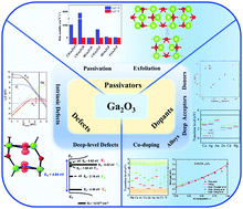
Ga2O3 is attractive for power devices and solar-blind ultraviolet photodetectors due to its ultra-wide bandgap, large breakdown field, and favorable stability. However, it is difficult to prepare the ideal Ga2O3 since there are plenty of defects (e.g., vacancies and interstitial atoms) in the bulk and films which can affect the physical properties of Ga2O3. Besides, the deep level defects act as trapped centers and have influence on the sensitivity and responsivity of optoelectronic devices. It has been discovered that doping is an effective strategy to modulate the properties of Ga2O3. In this review, the effects of defects and impurities on the material properties of Ga2O3 are mainly discussed. Considering that β-Ga2O3 is the most stable and the most studied currently, it is the main focus of this review. Firstly, the intrinsic properties (e.g., electronic, absorption, thermal and mechanical properties) of β-Ga2O3 are introduced, and then the influence of impurities (e.g., dopants and passivators) and defects on the electronic properties of β-Ga2O3 is discussed emphatically. Besides, the other properties (e.g., luminescence, magnetic, and piezoelectric properties) of β-Ga2O3 modulated by defects and impurities are also briefly discussed. Meanwhile, some new research directions are also worth exploring. These problems and potential directions are summarized and discussed in the last section.


image file: d2tc01128j-p1.tif

Yifei Wang

Yifei Wang obtained his BS in microelectronics science and engineering from Xidian University in 2019. From 2019 to the present, he studies in the State Key Discipline Laboratory of Wide Band Gap Semiconductor Technology at Xidian University, under the supervision of Prof. Jingjing Chang and Prof. Yue Hao. His current research focuses on the preparation of metal oxide-based thin-film transistors and photoelectric devices, and the materials simulation of wide bandgap semiconductors.

image file: d2tc01128j-p2.tif

Jingjing Chang

Prof. Jingjing Chang received his PhD degree from the National University of Singapore in 2014. After graduation, he worked as a Research Fellow in Materials Science & Engineering, National University of Singapore, from 2014 to 2015. Then he joined Xidian University, where he is currently a professor. His research interests include perovskite and metal oxide materials, electronic devices (transistors and RRAM devices) and optoelectronic devices (solar cells, photodetectors, and X-ray detectors).

image file: d2tc01128j-p3.tif

Yue Hao

Prof. Yue Hao received his PhD degree in computational mathematics from Xi’an Jiaotong University in 1991. He is the Vice president of Xidian University, professor, doctor, advisor of PhD candidates, a senior member of the IEEE, executive director of the Chinese Association of Electronics, chairman of the executive councils of the Shaanxi Provincial Association of Electronics, the Trade Association of Integrated Circuits, and the Shaanxi Provincial Semiconductor Illumination Association. His research interests include wide bandgap semiconductor materials and devices, reliability of ultra-deep submicron small-sized devices, SoC design, and its design methodology.


I. Introduction

Gallium oxide (Ga2O3), one of the ultra-wide bandgap (UWBG) semiconductors, has attracted more and more attention in recent years, as shown in Fig. 1.1–5 The literature on Ga2O3 exploded in the beginning of this century. Ga2O3 possesses many superior characteristics compared with other foregone semiconductors (e.g., SiC, GaN, GaAs, Si, and so on). For example, Ga2O3 single wafers with large areas can be prepared by scalable and low-cost melt growth techniques. Moreover, its large bandgap (Eg) ranges from 4.6 eV to 5.3 eV, and its breakdown field is up to 8 MV cm−1, which further improves its applications in high voltage devices, as shown in Fig. 2(a).6,7 The relationship between the on-resistance and breakdown voltage of common semiconductors is shown in Fig. 2(b). Such log–log plots represent Baliga's figure of merit (BFOM) of semiconductors which is a typical FOM for the low-frequency unipolar vertical power switch. Generally, the high voltage and low on-resistance properties of semiconductors facilitate generation of less heat and help obtain a similarly ideal situation at high voltage for the switch-type power device.7 Such characteristics are beneficial for developing efficient manufacturing processes and reducing the size and cost in the field of power switching devices. The ultra-wide bandgap semiconductor Ga2O3 possesses a higher BFOM than the traditional semiconductor so that Ga2O3 based devices provide more efficient power switching and energy savings than the devices based on Si, GaAs, SiC, and GaN.8 In addition, the large bandgap leads to its cut-off wavelength located in the deep ultraviolet region. The cut-off wavelength of Ga2O3-based photodetectors ranges from 250 nm to 280 nm, which meets the requirements of deep ultraviolet light (DUV) detection, as shown in Fig. 2(c).9 Meanwhile, the photodetectors based on Ga2O3 are insensitive to visible and infrared light, which improves the sensitivity of ultraviolet (UV) detection. In addition, the solar-blind photodetectors based on Ga2O3 can also overcome the shortcomings of other semiconductor-based photodetectors, e.g. AlxGa1−xN and MgxZn1−xO. That is, high temperatures are required when the Al component to be incorporated is high in photodetectors based on AlxGa1−xN (T > 1350 °C). The phase separation from wurtzite to the rock-salt structure occurs in photodetectors based on MgxZn1−xO when the Mg component is high.10–14 Besides, Ga2O3 has a relatively high density (6.44 g cm−3) and radiation resistance, as well as rapid scintillation and decay time constant of several nanoseconds, which makes it a promising candidate for nuclear radiation detection.15,16 Therefore, the applications of Ga2O3 are more and more extensive with the development of science and technology. Fig. 3 summarizes the frequently applied devices based on Ga2O3. The main application areas of Ga2O3 are photoelectronic detection, power devices, and some other applications (e.g., radiation detection, flame detectors, gas sensors, memory devices, and photocatalysts). The successful applications of these areas are related to the unique properties of Ga2O3 closely. To obtain high-performance devices based on Ga2O3, understanding the basic properties of Ga2O3 is indispensable in the process of device preparation and application.
image file: d2tc01128j-f1.tif
Fig. 1 Number of research studies on Ga2O3 as a function of time (data derived from Web of Science).

image file: d2tc01128j-f2.tif
Fig. 2 (a) Relationship between the breakdown fields and the bandgaps of different generation semiconductors. Reproduced with permission.6 Copyright 2012, American Institute of Physics Publishing. (b) Relationship between the breakdown voltages and switching resistances of different generation semiconductors. Reproduced with permission.235 Copyright 2014, WILEY-VCH Verlag GmbH & Co. KGaA, Weinheim. (c) The bandgap and wavelength range of GaN and Ga2O3 modulated by varying the alloy's composition. Reproduced with permission.377 Copyright 2017, Elsevier Ltd.

image file: d2tc01128j-f3.tif
Fig. 3 Schematic illustration of various device applications based on Ga2O3.

Ga2O3 has six phases (i.e., β-Ga2O3, ε-Ga2O3, α-Ga2O3, δ-Ga2O3, γ-Ga2O3, and κ-Ga2O3) and β-Ga2O3 is the most stable phase under ambient conditions. That is, the rest of the phases can be transformed into β-Ga2O3 under specific temperature, pressure, or other conditions. Therefore, most devices are based on β-Ga2O3 up to now. Note that Ga2O3 behaves as an insulator if it satisfies the stoichiometric ratio. However, the Ga2O3 prepared in the experiments behaves as an electron-rich (i.e., n-type) semiconductor instead of the so-called insulator. For example, intrinsic β-Ga2O3 contains a certain electron concentration (n = 1017–1018 cm−3) and mobility (μ < 200 cm2 V−1 s−1). However, the electron concentration is low and the mobility is far from the theoretical value (μ = 300 cm2 V−1 s−1).5,17–19 These cannot meet the criteria of high-performance devices. Besides, due to the unique Ga–O arrangement configuration, β-Ga2O3 can be exfoliated to obtain low-dimensional Ga2O3 which is considered to have potential applications in flexible electronic and optoelectronic devices.20–25 However, freshly exfoliated low-dimensional Ga2O3 is unstable and has no obvious quantum confinement effects, which will negatively affect the electronic performance and reliability of the devices. Therefore, it will hinder further applications based on low-dimensional Ga2O3 greatly.26,27 It has been found that the main reason for these unsatisfactory results is the defects in Ga2O3, e.g., vacancies, interstitial atoms, dangling bonds, and deep level defects, which are usually introduced in the preparation process. Therefore, it is very crucial to understand the mechanism of these defects and modulate the defects to design and obtain high-performance Ga2O3 materials and devices. Doping engineering and passivation engineering are important methods to modulate the material properties of semiconductors. On the one hand, substituting host atoms with suitable impurity atoms can modulate the electronic properties of the doping systems, e.g., the electronic structure, carrier concentrations, and carrier mobility. On the other hand, it has a certain influence on the defects. It has been discovered that passivating the surface dangling bonds is essential for achieving high stability and excellent electronic properties of low-dimensional Ga2O3. Meanwhile, other material properties (e.g., magnetic, luminescence, scintillation, and piezoelectric) can also be modulated by doping engineering for application in other areas.

Herein, we summarize the recent progress on the effects of impurities and defects on the properties of Ga2O3. Because β-Ga2O3 is the most stable structure under ambient conditions, it is the focus of the present review, supplemented by the situations of low-dimensional Ga2O3 and other metastable Ga2O3. The basic properties of Ga2O3 are introduced firstly, and then other properties (e.g., electronic, magnetic, luminescence, scintillation, and piezoelectric) based on the host β-Ga2O3 modulated by impurities and defects are described in depth. Finally, the issues to be solved in this area and prospects in the future are given.

II. Basic properties

1. Polymorphs of Ga2O3

There are five commonly identified polymorphs of Ga2O3 including hexagonal phase (α-Ga2O3), monoclinic phase (β-Ga2O3), cubic defective spinel phase (γ-Ga2O3), cubic bixbyite phase (δ-Ga2O3), and hexagonal wurtzite phase (ε-Ga2O3).28–30 The formation energy coupled with the thermodynamic stability of these five polymorphs is ranked as β < ε < α < δ < γ.5 In recent years, another new phase, the metastable κ-Ga2O3, is also synthesized on sapphire.31–33 Note that any other metastable phases can be converted into β-Ga2O3 at high temperatures (400–700 °C) under special conditions, as shown in Fig. 4 schematically. Only β-Ga2O3 can be grown as bulk crystals from melts, fluxes, or gas phases, while other phases can be obtained as thin films or thick layers.34 Theoretically, the opinion that these metastable phases could not be transformed from β-Ga2O3 has been accepted for a long time. However, a recent study discovered that β-Ga2O3 could convert into α-Ga2O3 under high pressure by shock compression experiments.35 The phase transition condition between α-Ga2O3 and β-Ga2O3 was estimated to be 2.0–3.0 GPa, 1200–1500 K. In addition, the phase transition was also observed at high temperature and pressure, i.e. 19.2 GPa36 and 20–22 GPa37 or 21 GPa, 1873 K.38 It was reported that phase transitions initialized at relatively low pressures and then expanded to higher pressures, e.g., from about 6 GPa39 to 40 GPa,40 or from 13.6–16.4 GPa to 39.2 GPa.41 Note that the temperature increases the regrowth of β-Ga2O3; thus complete phase transition into pure α-Ga2O3 is almost impossible. Therefore, mixtures of the two phases are usually prepared under high pressure experimentally. The structure and properties of these phases of Ga2O3 will be discussed in detail in the subsequent sections. The intrinsic structural parameters and fundamental physical constants of these Ga2O3 polymorphs are summarized in Table 1.
image file: d2tc01128j-f4.tif
Fig. 4 Schematic diagram of six phase structures and their phase transition relationships in Ga2O3 (α-Ga2O3, β-Ga2O3, δ-Ga2O3, γ-Ga2O3, ε-Ga2O3, and κ-Ga2O3). Reproduced with permission.4 Copyright 2019, Elsevier Ltd.
Table 1 Crystal structures, lattice parameters, bandgaps, and electron effective masses of the Ga2O3 family
Phase Structure Space group Lattice parameters Bandgap (eV) Electron effective mass (me) Ref.
α Hexagonal R[3 with combining macron]c a = b = 4.98 Å, c = 13.43 Å, α = β = 90°, γ = 120° 5.2–5.3 0.276m0 80 and 81
β Monoclinic C2/m a = 12.23 Å, b = 3.04 Å, c = 5.80 Å, α = γ = 90°, β = 103.8° E g(indirect) = 4.69 eV 0.27m0–0.34m0 101–103
E g(direct) = 4.66 eV
Γ Cubic Fd[3 with combining macron]m a = b = c = 8.24 Å, α = β = γ = 90° 5.0(direct), 4.4(indirect) 45
δ Cubic Ia3 a = b = c = 9.52 Å, α = β = γ = 90° 45
ε Hexagonal P63mc a = b = 2.90 Å, c = 9.26 Å, α = β = 90°, γ = 120° 4.9–5.0 0.24m0 90 and 93
κ Orthorhombic Pna21 a = 5.05 Å, b = 8.70 Å, c = 9.28 Å, α = β = γ = 90° 4.62 31


β-Ga2O3. It is a typical monoclinic structure with the space group C2/m whose lattice constants are a = 12.21 Å, b = 3.04 Å, c = 5.67 Å, α = γ = 90°, β = 103.8°.42,43 β-Ga2O3 is a kind of anion-dense accumulation structure. The b-axis of the centrosymmetric unit cell is the two-fold rotational axis in the β-Ga2O3 cell. Each β-Ga2O3 unit cell has two inequivalent Ga sites (Ga(1) and Ga(2)) and three inequivalent O sites (O(1), O(2), and O(3)). Half of the Ga atoms are at Ga(1) sites, forming a slightly distorted tetrahedron with four O ions. The other half of the Ga atoms are located at Ga(2) sites, forming a highly distorted octahedron with six O ions. Each O(1) is threefold-coordinated, located at the intersection point of two octahedra and one tetrahedron. Each O(2) is threefold-coordinated, shared by an octahedron and two tetrahedra. Each O(3) is fourfold-coordinated, located at the corner of three octahedra and one tetrahedron.44–48 In the bulk β-Ga2O3, the Ga–O bond lengths are Ga(1)–O(1) = 1.853 Å, Ga(1)–O(2) = 1.833 Å, Ga(1)–O(3) = 1.803 Å, Ga(2)–O(1) = 2.077 Å, Ga(2)–O(2) = 1.940 Å, and Ga(2)–O(3) = 1.978 Å. The structure and lattice parameters of β-Ga2O3 are shown in detail in Fig. 5.48 These structural characteristics lead to low symmetry for β-Ga2O3, which leads to significant anisotropy in structural, optical, and electronic properties. Besides, β-Ga2O3 can be grown by the low-cost melt methods, e.g., Czochralski method (CZ method),49,50 edge-defined film-fed growth method (EFG method),51 floating-zone method (FZ method),52 and vertical Bridgman method.53 Meanwhile, the β-Ga2O3 film can also be realized by epitaxial methods, e.g., metal–organic chemical vapor deposition (MOCVD),54–58 mist-chemical vapor deposition (mist-CVD),59 halide vapor phase epitaxy (HVPE),60–62 laser molecular beam epitaxy (LMBE),63,64 pulsed laser deposition (PLD)65–69 and magnetron sputtering.70–73 Compared with the expensive costs of crystal growth of other wide bandgap semiconductors (e.g., GaN and SiC) and irrealizable wafer of other phases, β-Ga2O3 has advantages in crystal growth and large-scale applications. Therefore, state-of-the-art microelectronic and optoelectronic devices are almost based on β-Ga2O3 in Ga2O3's family.
image file: d2tc01128j-f5.tif
Fig. 5 Schematic diagram of the structure of the unit cell of β-Ga2O3.
α-Ga2O3. The formation of metastable Ga2O3 depends on the lattice structure of the substrate and the growth temperature. Since the metastable phase α-Ga2O3 possesses a similar structure and little lattice mismatches to sapphire, the high-quality metastable phase α-Ga2O3 can be deposited on sapphire substrates by heteroepitaxial methods, e.g., pulsed laser deposition (PLD),74 halide vapor phase epitaxy (HVPE),75 metal–organic chemical vapor deposition (MOCVD),76 low-temperature atomic layer deposition (ALD),77 and mist-CVD.78,79 α-Ga2O3 is a typical hexagonal crystal with the space group R[3 with combining macron]c, whose lattice constants are a = b = 4.98 Å, c = 13.43 Å, α = γ = 90°, β = 120°.80,81 Compared with β-Ga2O3, α-Ga2O3 has a larger bandgap (Eg = 5.2–5.3 eV). Meanwhile, α-Ga2O3 can form tunable component alloys with In2O3 and Al2O3, for example, α-(InxGa1−x)2O3 and α-(AlxGa1−x)2O3. Note that the α-(AlxGa1−x)2O3 alloy will not undergo phase transition when the Al component (x) varies in the range of 0–100%.82 Besides, the carrier concentrations in α-Ga2O3 can be modulated effortlessly. Thus, α-Ga2O3 has remarkable potential applications. In recent years, Sn or Si doped α-Ga2O3 is applied in the Schottky barrier diode (SBD) and metal–semiconductor field-effect transistors (MESFETs). For example, Shiojima et al. investigated the effects of annealing temperature on the interface contact properties of the doped α-Ga2O3 SBD.83 They found that both forward and reverse currents increased with 400 °C annealing due to thermal degradation and different electrode materials. Dang et al. proposed a cost-effective strategy to realize high-performance Sn doped α-Ga2O3 MESFETs.84 By optimizing the dimension of MESFETs, the on/off ratio could reach up to 2 × 10⁷, and the rectification ratio and reverse breakdown voltage were 6 × 10⁶ and ∼20 V, respectively. Compared with β-Ga2O3-based power devices, the performance of α-Ga2O3-based power devices has been improved summarily.
γ-Ga2O3. The space group of γ-Ga2O3 is Fd[3 with combining macron]m. Its lattice parameters are a = b = c = 8.24 Å, α = β = γ = 90°.45 It has a crystal structure similar to that of an ideal spinel (e.g., MgAl2O4). Different from the ideal spinel structure, Ga atoms in γ-Ga2O3 only occupy the octahedral sites. γ-Ga2O3 can be epitaxially grown on sapphire and spinel substrates by mist-CVD,85 molecular beam epitaxy (MBE),86 and PLD.87–89
δ-Ga2O3. It is a metastable phase with a body-centered cubic structure and the space group is Ia3. It is isomorphous with some bixbyite crystals (e.g., In2O3, and Mn2O3).4,90,91 The lattice parameters of δ-Ga2O3 are a = b = c = 9.52 Å, α = β = γ = 90°.45 Although Sharma et al. synthesized nano-structured δ-Ga2O3 by the chemical precipitation method, there were still some β-Ga2O3 components in the nano-film, which made it impure.92 Therefore, a relevant in-depth research study is still needed to prepare pure δ-Ga2O3 films.
ε-Ga2O3. Hexagonal ε-Ga2O3 is prepared by heteroepitaxial growth normally. The lattice parameters of ε-Ga2O3 are a = b = 2.90 Å, c = 9.26 Å, α = β = 90°, γ = 120°.90,93 Note that hexagonal ε-Ga2O3 has a larger spontaneous polarization (P(ε-Ga2O3) = 24.44 μC cm−2) compared with GaN.33,94 Inspired by the previous work on the AlxGa1−xN/GaN heterojunctions, high-density two-dimensional electron gas (2DEG) can be formed at the ε-(AlxGa1−x)2O3/ε-Ga2O3 interface without any intentional doping. It has been discovered that the 2DEG charge densities at the ε-(AlxGa1−x)2O3/ε-Ga2O3 interface can reach up to 1.4 × 1014 cm−2 by varying the barrier type and ε-AlGaO3 thickness.95 Meanwhile, charge contrast ratios over 1500 can be realized by the thick ε-Ga2O3 cap layer and thin ε-AlGaO3 layers. This phenomenon reveals its potential applications in modulation-doped field effect transistors (MODFETs), non-volatile memory, and neuromorphic applications.95,96
κ-Ga2O3. Orthorhombic κ-Ga2O3 has attracted scholars in recent years. κ-Ga2O3 was considered to be the orthorhombic ε-Ga2O3 incorrectly due to their similar crystal structure in the previous research. In 2017, Cora et al. investigated the real structure of the Ga2O3 film deposited by MOVPE on the α-Al2O3 substrate in detail.31 They discovered that the layer had a columnar structure perpendicular to the interface and its origin was related to the formation of small domains. By transmission electron microscopy (TEM), it was observed that O atoms of the Ga2O3 layer formed a densely packed structure along the c-axis, while Ga atoms and these O atoms formed tetrahedral and octahedral structures, respectively. Meanwhile, these two different geometric structures formed two types of polyhedral layers. The oxygen positions are similar with 4H-SiC (ABAC) type close-packed stacking. Furthermore, the detailed TEM results revealed that the microstructure was ordered in 5–10 nm large domains and each domain was found to belong to the orthorhombic (Pna21) structure, which was regarded as the structure of κ-Ga2O3. This phenomenon was different from that discovered in ε-Ga2O3, so this work laid a foundation for in-depth understanding of the correct structure of κ-Ga2O3. The lattice parameters of κ-Ga2O3 are a = 5.05 Å, b = 8.70 Å, c = 9.28 Å, α = β = γ = 90°.31 Furthermore, it has been discovered that κ-Ga2O3 can be prepared by pulsed-laser deposition (PLD),97 metal–organic vapor phase epitaxy (MOVPE),31,76 and HVPE.98,99 Note that recent research discovered that κ-Ga2O3 was expected to exhibit a larger spontaneous polarization (P(κ-Ga2O3) = 26.39 μC cm−2) along the c-axis compared with GaN and ε-Ga2O3. κ-Ga2O3 with expected spontaneous polarization and piezoelectric effects will be applied in high-performance power devices to form two-dimensional electron gas at the hetero-interface. Such features are expected to further improve the performance of HEMTs.

2. Electronic properties of β-Ga2O3

In terms of the electronic properties of β-Ga2O3, band structure, density of states (DOS) and transport properties are the focus, because they are related to device performance closely. The electronic structures of β-Ga2O3 calculated by density functional theory (DFT) are illustrated in Fig. 6(a). Here, the GGA functional and the HSE06 hybrid functional are applied to obtain the band structure of β-Ga2O3, respectively. Note that the bandgap derived from HSE06 is closer to the experimental bandgap, while the bandgap obtained from GGA is underestimated because the exchange–correlation terms of the two functionals are different. As shown in Fig. 6(a), the conduction band minimum (CBM) and the valence band maximum (VBM) are located at the Γ and M points, respectively, which leads to the indirect bandgap in β-Ga2O3. On the other hand, in most previous publications, β-Ga2O3 exhibits the direct bandgap in which both CBM and VBM are located at the Γ point.59,100 Since the difference of the VBM between the M and Γ points is less than 100 meV, the measured indirect bandgap (Eg(indirect) = 4.69 eV) is a little larger than the measured direct bandgap (Eg(direct) = 4.66 eV). Furthermore, it can be observed that the CBM is mainly contributed by the Ga 4s orbital in the DOS diagram (see Fig. 6(b and c)), and the dispersive degree is large. The electron effective mass of β-Ga2O3 is small, which is in the range of 0.27m0–0.34m0 obtained by first-principles calculations.101–103 The band structure and conclusions are in good agreement with the experimental results.104–106 Note that both theoretical and experimental valence bands of β-Ga2O3 show weak band dispersion. As shown in Fig. 6(b–d), combined with the relevant partial density of states (PDOS), the valence band maximum is mainly composed of O 2p orbitals, and the dispersive degree is small, thus it is flat. Although the VBM of β-Ga2O3 is mainly composed of p orbitals, the contribution of each p orbital component is not equal. The VBM is mainly contributed by the 2px and 2pz orbitals of O atoms. In general, the p shell contains three p orbitals, that is, px, py, and pz, which are dumbbell-shaped but in different stretching directions. Therefore, the three different components of p orbitals show anisotropy. The characteristics of orbital contributions connected with the band structure reveal the anisotropy of electronic properties from another perspective. Similar experimental and theoretical methods have also measured the bandgaps (Eg) and electron effective masses of other phases, as listed in Table 1.
image file: d2tc01128j-f6.tif
Fig. 6 (a) Band structure of bulk β-Ga2O3 obtained by the HSE06 functional (red solid line) and GGA functional (black solid line). (b–d) Partial density of states (PDOS) of bulk β-Ga2O3. Reproduced with permission.21 Copyright 2018, American Chemical Society. (e) Measured Hall-charge density as a function of 1000/T (the dashed line presents the fitting of the charge density calculated based on the charge neutrality equation). (f) Experimental and calculated dependence of the Hall mobility in different scattering mechanisms on the temperature. Reproduced with permission.378 Copyright 2019, American Institute of Physics Publishing.

As mentioned above, the electron clouds of the Ga 4s orbital are spherically symmetric so that the band dispersion of the CBM in the Brillouin zone is symmetrical. In other words, the electron effective masses of β-Ga2O3 obtained from the CBM exhibit the isotropic character. Note that the electron clouds of the s orbital have a large radius, which results in the large overlapping electronic conduction path. It is thought that the mean free path of electrons in β-Ga2O3 is greater than the chemical bond length of β-Ga2O3. As a result, the small electron effective masses of β-Ga2O3 suggest the high electron mobility in β-Ga2O3.4 However, such electron mobility is far lower than that of other wide bandgap semiconductors, such as 4H-SiC (∼1000 cm2 V−1 s−1) and GaN (∼1200 cm2 V−1 s−1).5,107 Moreover, the electron mobility of β-Ga2O3 (μexperiment = 20–170 cm2 V−1 s−1) is much lower than the theoretical expectation (μtheory = 300 cm2 V−1 s−1) in the experiments.17,18,108–111 On the one hand, the low mobility is attributed to a large number of internal defects in β-Ga2O3. Therefore, the modulations of defects are very urgent and vital to realizing high-performance β-Ga2O3 based devices. On the other hand, the reasons are attributed to the different scattering mechanisms of electrons within different temperature ranges and the complex vibration modes of phonons in β-Ga2O3. It has been discovered by exploring of the influence of temperature on the mobility of β-Ga2O3 that β-Ga2O3 is affected by strong electron–phonon interaction (EPI) effects. Unlike the traditional notions of carrier transport in Si and GaAs, the low symmetry β-Ga2O3 crystal contains a variety of phonon modes generally and the carrier transport mechanism is quite different. The lattice vibration will disturb the potential field of the periodic crystal with the variation of temperature in the low symmetry crystal. Thus, the phonon vibration modes will combine with electron motion. This results in that the mobility of electrons is affected by electron–phonon interaction effects. This EPI effect plays a pivotal role in controlling the mobility of intrinsic semiconductors, and the interaction is a long-range Coulomb interaction essentially. Unfortunately, this phenomenon cannot be avoided in a semiconductor with a low symmetry structure. Among them, the polarized optical phonon (POP) scattering which is one of the representatives of EPI effects has been investigated a lot because it is an important scattering mechanism at medium temperature (e.g., room temperature). Besides, as shown in Fig. 6(e and f), other mechanisms also affect the carrier mobility in β-Ga2O3, e.g., ionized (μII) scattering, neutral impurity (μNI) scattering, and acoustic deformation potential scattering (μADP). Through theoretical analysis, the values of the Hall mobility at different temperatures after being affected by these scattering mechanisms are listed in detail.

In the bulk β-Ga2O3, the long-range interaction controls the intrinsic electron transport. In this condition, the same dipole moment is produced by transverse optical (TO) and longitudinal optical (LO) vibrational mode splitting at the long-wavelength limit. The LO modes gain slightly higher energy than their TO counterparts. The electron and LO modes are coupled in the long-range EPI effect. This coupling is polar and the scattering resulting from this coupling is regarded as POP scattering. At low temperatures, the POP scattering effect in β-Ga2O3 is weak and the impurity scattering plays a dominant role. As the temperature increases gradually, the electrons’ energy also increases and the ionized impurity scattering decreases, which increases the bulk electron mobility. In addition, POP scattering attempts to dominate with a further increase in temperature. The rate of POP scattering increases with increasing temperature due to the increase in the Bose occupancy number. Therefore, the bulk electron mobility begins to drop. As mentioned earlier, the bulk mobility in β-Ga2O3 at moderate temperature is also affected by other scattering mechanisms. However, according to the Fermi-Golden rule, the effects of these scatterings on bulk electron mobility are small compared with that of POP scattering. They can be ignored when investigating the transport problems in β-Ga2O3 generally. It is discovered that the POP scattering effect is the main culprit in reducing the bulk electron mobility in bulk β-Ga2O3 in the range of moderate temperatures. To suppress the POP scattering, one possible solution is to screen the POP modes. This strategy needs higher carrier concentrations in the bulk β-Ga2O3.

Unfortunately, the carrier concentrations in intrinsic β-Ga2O3 are so low that the POP scattering is unable to be suppressed. Low carrier concentrations and mobility result in low electrical conductivity (σ) so that it limits the device performance of β-Ga2O3. Doping is an available strategy to tune the properties of semiconductors. In general, substitution doping with external atoms different from host valence electrons will modulate the properties of semiconductors. In β-Ga2O3, the incorporation of some electron-rich metals (e.g., Sn, Si) can increase the carrier concentrations by orders of magnitude. Nevertheless, electron mobility still fails to reach the theoretical value (less than half of the theoretical value).112 To obtain electrons with high mobility, the electron transport path needs to be optimized to satisfy the features of less scattering, and the two-dimensional electron gas (2DEG) matches these conditions. Therefore, the device performance can be improved by obtaining two-dimensional electron gas to improve carrier mobility. It has been discovered that two-dimensional electron gas with high mobility can be formed by modulation doping at the (AlxGa1−x)2O3/Ga2O3 heterojunction interface. Therefore, the mobility of 2DEG (>100 cm2 V−1 s−1, μmax = 1000 cm2 V−1 s−1) will be higher than that in the bulk through reasonable modulated doping and band matching of the heterojunction interface; then electrons with high mobility are expected to be realized in Ga2O3.18,110,113,114

3. Absorption and transmittance properties

As an ultra-wide bandgap semiconductor, β-Ga2O3 has high transmittance and low absorption in the visible and near-infrared regions of the solar spectrum, and hence it can be applied in transparent conductive electrodes in some areas.115,116 Meanwhile, the absorption cutoff edge and the maximum absorption peak are located in the ultraviolet region, and it has strong absorption in the solar-blind ultraviolet region. It is noted by polarized optical absorption and reflectance measurements that the light absorption of β-Ga2O3 in three different directions of [100], [010], and [001] is also different, as shown in Fig. 7(a), suggesting anisotropy in the optical properties of β-Ga2O3. Although the absorption situations are different in the three different directions, the absorption intensity is weaker in the low-energy region and greater in the high-energy region. According to the absorption coefficient curve derived from the Tauc plot method, the optical bandgaps of β-Ga2O3 are different in three different directions. Fig. 7(a) shows that the bandgap along the [010] orientation is the largest (Eg[010] = 4.850 eV), while the optical bandgap along the other two directions ([100] and [001]) is 4.585 eV and 4.560 eV, respectively. Onuma et al. applied a 300 W Xe lamp to measure the optical absorption and transmittance at room temperature.117 In addition to the anisotropic light absorption, the transmittance of β-Ga2O3 in different directions was also investigated (see Fig. 7(b)). The transmittance of Eb orientation is higher than that of Ea and unpolarized orientation. Furthermore, they revealed the absorption and transmittance mechanism by using experimental results coupled with theoretical calculations, as shown in Fig. 7(c). Such anisotropic optical absorption and transmittance can be explained by the inconsistent band-to-band transition. Each primitive cell contains the following bands, called Γ1+, Γ2+, Γ1, and Γ2+ bands. The CBM is isotropic and is expressed as the Γ1+ band. Except for the transitions from the Γ1+ and Γ2+ bands to the Γ1+ band of the CBM which are dipole forbidden, the other band-to-band transitions are dipole allowed. Therefore, the transitions from the rest of the different bands of the VBM to the Γ1+ band of the CBM represent optical properties in different directions.46,117–119 This explains the anisotropy in the optical properties of β-Ga2O3 reasonably.
image file: d2tc01128j-f7.tif
Fig. 7 (a) Polarization-dependent absorption edge of bulk β-Ga2O3 crystal samples obtained by the Czochralski method. Reproduced with permission.42 Copyright 2018, IOP Publishing Ltd. (b) Unpolarized (blue solid line) and polarized (purple and orange solid lines) transmittance spectra of the (001) undoped β-Ga2O3 substrate at room temperature. (c) Irreducible representations and rough transition process of the band structure in β-Ga2O3. The horizontal solid and dotted lines represent the valence bands for the dipole allowed and forbidden transitions at Γ, respectively. The vertical solid lines represent the rough transition process. Reproduced with permission.117 Copyright 2015, The Japan Society of Applied Physics.

4. Thermal and mechanical properties

Although β-Ga2O3 has many excellent properties that have attracted scholars, there are still many troublesome problems which need to be overcome. Thermal conductivity (κ) is an important parameter that severely affects the performance and reliability of devices including both power devices and optoelectronic devices. There are several methods to obtain the thermal conductivity of β-Ga2O3. The theoretical method may involve independent first-principles calculations or could be coupled with machine learning.120 The experimental methods are the 3ω method and the time domain thermo-reflectance (TDTR) method.121,122 Due to the continuous optimizations and updates of calculation methods, the theoretical thermal conductivity (e.g., κ[010] = 20.00 W m−1 K−1,123 21.54 W m−1 K−1[thin space (1/6-em)]124) has been very close to the experimental value (e.g., κ[010] = 21.00 W m−1 K−1[thin space (1/6-em)]125). Therefore, the scholars use theoretical calculations to predict and then evaluate the thermal properties rather than complex experiments. Note that the thermal conductivity of β-Ga2O3 is lower than that of some semiconductors commonly applied up to now, e.g. κGaN = 240.00 W m−1 K−1,126–128κSi = 140.00 W m−1 K−1,129 and κSiC = 350.00 W m−1 K−1.129 The low thermal conductivity of β-Ga2O3 needs more in-depth research on the internal mechanism, which should be noticed in device applications. Galazka et al. measured the thermal conductivity of β-Ga2O3 along the [010] direction by applying the laser flash diffusivity method, where the thermal conductivity decreased with increasing temperature in the range of 20–1200 °C.125 They found that the point defect scattering played a major role in the thermal conductivity at low temperature, while the phonon–phonon Umklapp scattering gradually dominated at high temperatures (above 150 K). Note that the thermal conductivity of β-Ga2O3 is anisotropic due to the low symmetry structure. Guo et al. investigated the four different orientations in the β-Ga2O3 bulk by the time domain thermo-reflectance (TDTR) method.122 They measured the thermal conductivity of different orientations by varying the temperature and found that the thermal conductivity decreased as the temperature increased in general, as shown in Fig. 8(a and b). Based on the verification of previous studies, they also found that the reason for anisotropic thermal conductivity was due to the discrepancies in the speed of sound along different crystal orientations.
image file: d2tc01128j-f8.tif
Fig. 8 (a) Temperature-dependent thermal conductivity in the log scale along different crystal orientations of β-Ga2O3 by the TDTR approach as a function of temperature (K). (b) Temperature-dependent thermal conductivity in the linear scale along different crystal orientations of β-Ga2O3 by the TDTR approach as a function of 1/T (K−1). Reproduced with permission.122 Copyright 2015, American Institute of Physics Publishing. The direction-dependent (c) Young's modulus and (d) shear modulus of bulk β-Ga2O3 in 3D representation surfaces. Reproduced with permission.132 Copyright 2019, Elsevier Ltd.

The thermal coefficients are related to the mechanical coefficients in the process of investigating other crystal properties. As for monoclinic β-Ga2O3, it has 13 kinds of elastic constants (C11, C22, C33, C44, C55, C66, C12, C13, C15, C23, C25, C35, and C46).23,130–132 They are usually obtained by first-principles calculations, as well as Young's modulus E, bulk modulus B, shear modulus G, and other mechanical constants. Note that the obvious differences of these mechanical constants in different orientations indicate that the mechanical properties of the bulk β-Ga2O3 are anisotropic obviously. Fig. 8(c and d) displays the 3D representation surfaces of direction-dependent Young's and shear moduli of bulk β-Ga2O3, respectively. It is not a common sphere and has different values in different directions, that is, it is anisotropic. Meanwhile, the minimum thermal conductivity κmin is closely related to the above elastic properties and can be obtained by the following formula: image file: d2tc01128j-t1.tif, where kB, NA, N, ρ, E, and M are the Boltzmann constants, Avogadro's number, the number of atoms in the unit cell, density, Young's modulus, and the weight of the unit cell, respectively.23,133,134 Therefore, this also explains the reasons for the different thermal conductivity of bulk β-Ga2O3 in different directions observed in the experiment from another aspect.

In addition, it has been found that C11 is less than C22 and C33, while C55 and C66 are greater than C44, suggesting that the bond strength along the [100] direction of bulk β-Ga2O3 is weaker than that in other directions. Thus, it can be sliced into quasi two-dimensional flakes along the (100) surface. The exfoliation energy of β-Ga2O3 along the (100) surface is calculated by the DFT method, as shown in Fig. 9(a).21 The mechanical properties of low-dimensional Ga2O3 after exfoliation also have great variations compared with that of bulk. For example, the anisotropies in the compressive and shear behaviors in the monolayer Ga2O3 are enhanced as shown in Fig. 9(b and c). Their shapes are far from sphere shapes. Meanwhile, the modulus B, G, and E of monolayer Ga2O3 decrease (see Fig. 9(d)) while the thermal constant κ increases up to 49 W m−1 K−1.23 It is expected to alleviate the heat dissipation problem caused by the poor thermal conductivity in the bulk Ga2O3.


image file: d2tc01128j-f9.tif
Fig. 9 (a) Calculated exfoliation energy in different crystal planes as a function of dd0. Reproduced with permission.21 Copyright 2018, American Chemical Society. The direction-dependent (b) Young's modulus and (c) shear modulus of low-dimensional Ga2O3 in 3D representation surfaces. (d) Bulk modulus (B), shear modulus (G), and Young's modulus (E) of the bulk and different layers of low-dimensional Ga2O3. Reproduced with permission.132 Copyright 2019, Elsevier Ltd. (e–g) PDOS of H passivated low-dimensional Ga2O3. (h) Band structure of monolayer low-dimensional β-Ga2O3 obtained by the HSE06 functional (red solid line) and GGA functional (black solid line). (i) Projected charge densities of the CBM and VBM of H passivated low-dimensional Ga2O3. Reproduced with permission.21 Copyright 2018, American Chemical Society.

Unluckily, this exfoliation property is not observed in other metastable Ga2O3 up to now. As mentioned above, β-Ga2O3 is composed of a chain structure in which [GaO4] tetrahedra intersect with [GaO6] octahedra. Because the atoms in the crystal need to meet the rule of the dense packing properties, the O atoms and Ga atoms at the interface between [GaO4] tetrahedra and [GaO6] octahedra often have long bond lengths. This is the unique feature of this crossed chain structure. In contrast, the lattice structures of other phases are composed of only [GaO6] octahedra, which are not easy to exfoliate into the low-dimensional structure. Thus, the subsequent research is mainly based on the low-dimensional Ga2O3 obtained from exfoliated β-Ga2O3.

5. Low-dimensional Ga2O3

Due to the unique structure of β-Ga2O3, the low-dimensional structure can be obtained by exfoliating the bulk β-Ga2O3. As the thickness of the material decreases to the atomic thickness, the properties change accordingly. However, since β-Ga2O3 is not a van der Waals material, obtaining ultra-thin flakes with a thickness of less than 100 nm is a huge challenge. Kwon et al. solved this problem in 2017.135 They mechanically exfoliated the bulk β-Ga2O3 with tape and then applied plasma etching to tune the thickness of exfoliated Ga2O3. Combined with the SF6 atmosphere, the thickness of the β-Ga2O3 flake could be tuned from 300 nm down to ∼60 nm. Because the reaction between SF6 and Ga2O3 generated oxygen and volatile oxyfluoride compounds, and non-volatile compounds (e.g., GaFx) that can be moved by ion bombardment, the thickness of exfoliated Ga2O3 can be reduced. Meanwhile, Van de Walle et al. and Bermudez attempted to thin the thickness of β-Ga2O3 along the [100] orientation down to half to attain the monolayer β-Ga2O3 theoretically and then investigated the properties of monolayer β-Ga2O3 briefly.48,136 In the process of exploring the transport properties of low-dimensional Ga2O3, the carrier mobility (∼130 cm2 V−1 s−1) of β-Ga2O3 membranes exfoliated by Hwang et al. was found to be close to that of the bulk.22 However, the mobility value is still not comparable to those of other wide bandgap semiconductors. The lack of quantum confinement effects has been observed in the unpassivated β-Ga2O3 flake. What's more, the exfoliated Ga2O3 is unstable under ambient conditions because of the dangling bonds on the surface. It is found that surface passivation technology is one of the good solutions to the instability of low-dimensional wide bandgap semiconductors.137 Based on previous research results, Su et al. did further research on exfoliated Ga2O3 by surface passivation engineering.21,27,132,138 They put forward a new strategy for applying hydrogen to passivate the surface of low-dimensional Ga2O3, which further enhanced the quantum confinement effects. They found that the H passivated structure demonstrated a larger bandgap (5–6 eV) and higher carrier mobility (∼25[thin space (1/6-em)]000 cm2 V−1 s−1), which led to its application in optoelectronic devices. Meanwhile, samples with hydrogen passivation had a long electron relaxation time (∼4 ps) and larger exciton binding energy (1–2 eV) than the bulk. Although some theoretical studies have been carried out on low-dimensional Ga2O3, it still needs to be confirmed by subsequent related experiments. In addition to the mechanical exfoliation mentioned above, it should be noticed that the low-dimensional Ga2O3 monolayer can also be obtained by the chemical synthesis method and MBE, but the exfoliation method is widely applied because of its simple process.139,140

Although H passivated monolayer Ga2O3 has many excellent properties, there are still some problems that need to be solved, e.g., many defects in the parent bulk Ga2O3 are also accompanied by the monolayer Ga2O3 during the exfoliation. Besides, similar to the bulk Ga2O3, the VBM of monolayer Ga2O3 is still mainly contributed by the 2p orbitals of O, as shown in Fig. 9(e and g). The dispersion degree of monolayer Ga2O3's valence band is low (see Fig. 9(h)), and the effective mass of the hole is large, which affects the hole transport. Meanwhile, the generated holes do not become free holes instead of the localized holes formed near the O atoms (see Fig. 9(i)). Effective p-type doping is difficult to be obtained. Therefore, investigating the effects of impurities and defects on the properties of low-dimensional Ga2O3 is similar to the situation in the bulk Ga2O3 to a degree.

III. Effects of defects and impurities on electronic properties

Although β-Ga2O3 has been fabricated by several methods, there are inevitable defects (e.g., vacancies, deep level defects, etc.) in β-Ga2O3 which significantly affect the properties of β-Ga2O3 and the performance of β-Ga2O3 based devices.52,141 On the one hand, defects can serve as scatter centers to affect the carrier mobility and then affect the device output characteristics and responsive characteristics. On the other hand, they can also serve as trapped centers which affect sensitivity in the photodetectors. In addition to the bulk defects, the surface and interface defects of β-Ga2O3 are also associated with poor device performance, such as threshold voltage instability, reduced channel carrier mobility, and poor device reliability. Therefore, the defects including vacancies and interstitial atoms in the β-Ga2O3 host material are worth to be studied.

Metal oxides are insulators under the condition of meeting the stoichiometric ratio, but their growth has a great relationship with the composition of the ambient atmosphere in the actual process. The insufficiency or excess of O atoms in the chemical composition results in oxygen vacancies (VO) or oxygen interstitials (Oi), respectively.142,143 VO and Oi play the roles of donor and acceptor, respectively, thus making the conductivity of oxides vary with the oxygen content at room temperature, as shown in Fig. 10(a). Meanwhile, considering the differences of growth environments such as Ga rich and O rich, other single defects (VGa and Gai) and double defects also exist in β-Ga2O3.144 Besides, some impurities inevitably enter β-Ga2O3 crystals and act as impurities in the actual growth process of bulk β-Ga2O3; for example, hydrogen (H) and Si impurities, etc., even form complexes with the vacancies in the host.105,145–147 Meanwhile, the Ir ions are observed in the bulk β-Ga2O3 due to the utilization of crucible in the melt method in recent years.148 These dopants introduced unintentionally during the preparation are deemed unintentional dopants. The unintentional dopants are related to the raw materials and vessels applied in the preparation closely, and they are generally unavoidable. Therefore, they are considered to be another origin of n-type performance in intrinsic β-Ga2O3.


image file: d2tc01128j-f10.tif
Fig. 10 (a) The electrical conductivity of the β-Ga2O3 single crystals along the b axis as a function of the O2 flow rate. The closed circles and the open square refer to samples grown from undoped and Sn-doped Ga2O3, respectively. Reproduced with permission.46 Copyright 1997, American Institute of Physics Publishing. (b) Relaxed atomic configurations and iso-surfaces of the squared wave functions of the STHs on the O1 and the O3 site in β-Ga2O3. Reproduced with permission.379 Copyright 2019, American Physical Society. Formation energies of point defects (e.g., VGa, VO, Gai, and Oi) in β-Ga2O3 as a function of the Fermi energies in (c) O-poor and (d) O-rich conditions. Reproduced with permission.146 Copyright 2013, American Physical Society. (e) Four processes of capture and emission of carriers between deep-level defects and the valence band (VB) or the conduction band (CB) in terms of the well-known Shockley–Read–Hall model. Reproduced with permission.380 Copyright 2021, IOP Publishing Ltd.

The electronic performance of devices needs to be further modulated in the applications of β-Ga2O3 devices. Doping engineering is an effective method. The available dopants, e.g., Si,149 Ge,150 Sn,141etc., are commonly applied in β-Ga2O3. These dopants tune the electron concentrations of β-Ga2O3 ranging from 1015 to 1021 cm−3, which meet the basic requirements of high-performance devices. However, effective p-type doping, the troublesome question, is difficult to be realized in β-Ga2O3 due to the flat valence band, self-trapped effects, and so on.151,152 The self-trapped effects in β-Ga2O3 are generally induced by the lattice distortion.153 Self-trapped charges are localized and the wave function of the electrons is only localized around the O atoms but not involved in the whole crystal, as shown in Fig. 10(b). This has also been confirmed by some characterization methods, e.g., deep-level transient spectroscopy (DLTS) and deep-level optical spectroscopy (DLOS). The conditions are also observed in other wide bandgap oxides such as ZnO, SnO2, and In2O3.154 Since the existent defects and impurities have significant effects on the fabrication and application of β-Ga2O3, understanding the physical properties of defects and impurities of β-Ga2O3 is of great significance. Meanwhile, the significance of obtaining p-type Ga2O3 is not only to overcome the problems of Ga2O3 itself but also to some extent to provide guidance for effective p-type doping of other wide bandgap oxide semiconductors.

In the following section, the common defects and impurities in β-Ga2O3 are summarized, e.g., vacancies and interstitial atoms, deep level defects, unintentional doping impurities, available doping impurities, and surface passivators. The intrinsic defects of bulk β-Ga2O3 and the effects of donors, acceptors, and passivators on the electronic properties are described. Meanwhile, the effects of defects and impurities on the electronic properties of low-dimensional β-Ga2O3 are comparatively reviewed here.

1. Intrinsic defects

1.1 Oxygen vacancy (VO). Note that both bulk β-Ga2O3 grown by the melt method and epitaxial film obtained by vapor deposition often show a certain conductivity after the growth process or subsequent heat treatment in the atmosphere of N2, H2, or vacuum. Moreover, the conductivity (σ) of β-Ga2O3 varies with the oxygen flow conditions, as shown in Fig. 10(a).52 Specifically, β-Ga2O3 has high conductivity at a low O2 flow rate and it decreases with increasing O2 content. These treatments significantly tune the concentrations of oxygen vacancies (VO) in β-Ga2O3. Therefore, the conductivity of β-Ga2O3 is related to the O2 content in the atmosphere, which is related to the oxygen vacancy (VO) concentrations in β-Ga2O3. The VO is regarded as the donor, and the carriers ionized by VOs will further increase the background carrier concentrations in the undoped Ga2O3 bulk or film. For example, Lee et al. prepared β-Ga2O3 thin films by magnetron sputtering, and then annealed them in the O2 and N2 atmosphere, respectively.155 Dong et al. annealed the sputtered β-Ga2O3 thin film in an atmosphere of O2 of different volume percentage.156 They all found that the conductivity of the as-grown Ga2O3 film also varied with the variation of O2 content in the annealed atmosphere. They suggested that VO which played the role of a donor provided additional carriers based on X-ray photoelectron spectroscopy (XPS). In the O 1s XPS spectra, two main peaks can be obtained by the fitting of the O 1s peak by Gaussian fitting. The strongest peaks with binding energies of 531.6–531.9 eV were assigned to lattice oxygen (i.e., Ga–O bond), and the peaks with the highest binding energy around 532 eV were assigned to oxygen vacancy (VO) in general.157–167 The as-grown Ga2O3 films were post-annealed in the O2 and N2 atmospheres respectively in Lee et al.'s research. The O content increased more in the O2 environment (O/Ga = 1.43) than in the N2 environment (O/Ga = 1.42). Meanwhile, the carrier concentrations of the films obtained by the CV measurement in O2 and N2 atmospheres were 1.62 × 1016 cm−3 and 2.01 × 1016 cm−3, respectively. Thus, it can be derived from the experiments that the variation of carrier concentrations and electrical conductivity was commonly caused by oxygen vacancies (VOs). The related mechanism is that an oxygen vacancy (VO) often captures two electrons to maintain its neutral oxygen vacancy. Free electrons can be ionized by single or double neutral oxygen vacancies in β-Ga2O3. This mechanism allows β-Ga2O3 to produce excess electrons to behave as an electron-rich oxide. Thus, β-Ga2O3 shows conductivity upon annealing in the absence of an oxygen atmosphere. The VO is presumed to introduce a shallow donor level, which will provide electrons to increase the carrier concentrations and further increase the conductivity. Meanwhile, it is found that the VO is a shallow donor level located at about ∼0.02–0.03 eV below the CBM in the experiment.168 However, the viewpoint that the conductivity of β-Ga2O3 is induced by VOs is refuted by other results. Zacherle et al. found the related phenomena.143,169–171 Although VOs were easily formed at the low oxygen partial pressure, the transition level from the neutral state to the +2 state was the deep level in the bandgap whether in the O-rich or O-poor ambient condition, as shown in Fig. 10(c and d). One of the three types of VOs (VO(2)) in β-Ga2O3 was close to the CBM, and the other two (VO(1) and VO(3)) were far away in the ΔEformEFermi diagram. However, the defect level E(0/+2) introduced by VO(2) close to the conduction band was still more than 1 eV (i.e., EcE(0/+2) > 1 eV), which had also been obtained in other literature.171–173 This indicated that the VO was a deep-level defect. Moreover, Onuma et al. found that the blue emission was observed in β-Ga2O3, which was attributed to the recombination between the deep local donor and the trapped hole.174,175 The deep-level donor states here were speculated to be derived from VOs. The deep defects may not increase the electron concentrations.105,143,172 This phenomenon is similar to the case in other oxides, e.g., ZnO and In2O3.176 In addition, the deep VO states are also confirmed by deep level transient spectroscopy (DLTS), deep resolution cathodoluminescence spectroscopy, and surface photoelectric voltage spectroscopy.177,178 The results show that the distance from the defect level related to VO to the CBM is over 1 eV. Thus, whether the oxygen vacancy (VO) is the main source of n-type conductivity for β-Ga2O3 is still worth discussing and investigating.

As discussed in the previous section, the intrinsic defects (e.g., VOs) cannot be avoided in the low-dimensional Ga2O3 due to the direct exfoliation from the parent β-Ga2O3 bulk, which will have significant impact on the electronic properties of low-dimensional Ga2O3. To explore the effects of ordinary vacancies and explain the mechanism of defective low-dimensional Ga2O3, defective low-dimensional Ga2O3 models were constructed and explained theoretically by Sun et al.179 They found that the effects of defects on the low-dimensional Ga2O3 were similar to that in the bulk. For example, the VOs introduced impurity states into the bandgap, which further reduced the bandgap and affected the performance of low-dimensional Ga2O3.

In general, VOs existing in the bulk β-Ga2O3 are considered as annoying defects in the power and optoelectronic devices. VO hinders the fabrication of bipolar devices because the p-type Ga2O3 is difficult to obtain as mentioned before. That is, VO has been regarded as the donor in much research, especially in devices based on thin films grown by physical vapor phase epitaxy. It ionizes several electrons to increase the background carrier concentrations in Ga2O3 and then compensates the acceptor dopants which have a low ionization rate to decrease the hole concentrations. Therefore, researchers have to consider applying a combination of heterogeneous p/n-type semiconductor materials in forming bipolar transistors or field-effect transistors in complementary devices and circuits technology. Besides, VOs as the trapped centers affect the sensitivity and responsivity in optoelectronic detectors, which should be noticed in the actual applications.

Effective ohmic-type metal–semiconductor contacts are important steps in the fabrication of transistors. In field-effect transistors based on metal-oxides, ohmic contact is often expected to be realized by the production of many VOs in the semiconductor at the interface of field-effect transistors. In the fabrication of β-Ga2O3 based transistors, Ti is chosen as the direct contact layer with β-Ga2O3, and Au is deposited upon Ti. The ohmic contact between Ti/Au and Ga2O3 is formed by rapid thermal annealing (RTA) in a N2 atmosphere in the range of 450–500 °C.107,180,181 Because the O atoms located at the Ti–Ga2O3 interface upon annealing in the absence of oxygen can spread into Ti contacted with Ga2O3 to form TiOx, the interface at Ga2O3 forms lots of VOs. This reduces the contact barrier located at the interface of Ga2O3, enabling easy formation of the ohmic contact. As for the non-volatile storage area, e.g., resistance random access memory (RRAM), VOs are of great benefit for device applications.182–184 The conductive filament model composed of the oxygen vacancies is the main conduction mechanism of RRAM. The switching between low and high resistance states (LRS and HRS) in the resistive memory is carried out by the formation and disconnection of VO conductive filaments in the Ga2O3 layer, which is expected to update the existing von Neumann architecture of memory.

1.2 Gallium vacancy (VGa). Different from the VO, gallium vacancy (VGa) is a p-type acceptor defect which may be formed in β-Ga2O3 under the O-rich condition in theory. In recent years, Zacherle et al. obtained the formation energy and defect levels of VGa by first-principles calculations, as shown in Fig. 10(c and d).185 Gallium vacancy (VGa) promotes β-Ga2O3 to form a p-type semiconductor theoretically, that is, the Fermi level (EF) is close to the valence band. However, the formation energy of VGa is very large in this situation, indicating that VGa is not easy to form. Although the formation energy of VGa decreases significantly as the Fermi level approaches the CBM of Ga2O3, the expected p-type Ga2O3 is not observed in the experiments. The phenomenon that the formation energies of cation vacancies are too high to realize p-type semiconductors can be discovered in other oxides, e.g., ZnO and In2O3.143,186,187 In order to further determine the existence of VGa and its possible compensation effects in Ga2O3, positron annihilation spectroscopy is applied to explore the compensation of vacancy defects in Ga2O3 films in terms of experiments.188 The conclusion reveals that the compensation is not constrained by cation vacancy. Similar results can be obtained by other research.105,170,189,190 Moreover, advanced detection methods of defects in the materials provide convenience for locating deep defect levels in materials. Polyakov et al. discovered the deep acceptor level by low-temperature photo-capacitance and capacitance–voltage measurement. The acceptor level was regarded as VGa and it was located at the position of Ev + 2.5–2.8 eV.178,191,192 Meanwhile, they found another VGa in the gap located at the position of Ev + 1.3 eV by deep level transient spectroscopy with electrical and optical excitation (DLTS and ODLTS).193 Therefore, VGa is a deep acceptor defect and does not contribute to the p-type conduction in Ga2O3. It is difficult to realize p-type Ga2O3 by VGa in the host material. Although the formation energy of a single VGa is very high and it is hard to realize, the formation of other defects will induce the VGa generated in the experiments, for example, the H treatment discussed in the “Unintentional doping mechanism” section.
1.3 Oxygen and gallium interstitials (Oi and Gai). Gallium and oxygen interstitials (Gai and Oi) play the roles of donor and acceptor respectively in principle. They have some effects on n-type conduction and p-type conduction. However, the theoretical calculations show that their formation energies are higher than that of other defects, and therefore the concentrations of these defects are less in β-Ga2O3 crystals, as shown in Fig. 10(c and d).143,146 Their effects on the whole defective systems' properties can be ignored normally.
1.4 Deep-level defects. Deep-level defects are noteworthy defects in semiconductors because they have strong effects on carriers’ capture and recombination although they have weak influence on carrier concentrations and conductivity. These deep-level defects are investigated by deep-level transient spectroscopy (DLTS) and deep-level optical spectroscopy (DLOS). The detective fundamental is the Shockley–Read–Hall model which contains the excitation and capture of the carriers at the defect level, as shown in Fig. 10(e). The excitation and recombination of carriers can occur not only between the conduction band and the valence band but also between the conduction band/valence band and defect levels in the bandgap. Five kinds of deep levels (viz. E1,…,E5) have been reported in the Ga2O3 bulk and films, as shown in Fig. 11(a). By using DLTS, Zhang et al. observed that the E1, E2, and E3 levels were located at 0.62 eV, 0.82 eV, and 1.00 eV from the CBM, respectively.178 Similar positions of these deep levels were also found by Irmscher et al. and Farzana et al.192,194 The other two deep defect levels named E4 and E5 respectively were observed by DLOS. They were located at 2.16 eV and 4.40 eV from the CBM, respectively. These deep levels were often located in the bandgap as compensation levels or trapped centers. Other researchers have also observed deep defect levels in bulk or thin film Ga2O3. The positions of these deep defect levels are listed in Table 2. There are many speculations about the origin of these deep levels. It is inferred that the source of deep level E1 may be assigned to transition metal (such as Fe and Co) doping, while the source of E2 may be caused by Sn doping or Fe doping. In addition, it may also be attributed to VO. The source of the E3 level may be related to transition metal doping or VO. Moreover, the results detected in the epitaxial layer suggest that it may also be related to the complex formed by H and intrinsic defects. E4 is related to the intrinsic defects or VGa coupling with H. The concentrations of E5 in bulk materials are high up to 1016 cm−3, which is considered to be related to VGas or self-trapped holes (STHs). Besides, it is interesting to find that there is an image file: d2tc01128j-t2.tif level at 0.72 eV below the conduction band, which may originate from VGas or their complexes. It should be noticed that the concentrations of these defects are different in bulk and epitaxial films, as shown in Table 2. Meanwhile, the concentrations of E2 and E4 levels increase under the proton irradiation condition, which proves that the origin of these two deep levels is related to the intrinsic defects in Ga2O3. This character can be also applied to examine the damage of proton irradiation.
image file: d2tc01128j-f11.tif
Fig. 11 (a) Summary of the distribution of deep level defect states detected by both DLTS and DLOS in the same EFG-grown β-Ga2O3(010) materials. Reproduced with permission.178 Copyright 2016, American Institute of Physics Publishing. (b) Schematic diagram of O2 delivery to the growth furnace for growing large diameter β-Ga2O3 single crystals from an Ir crucible as a function of temperature by the melt-grown method. Reproduced with permission.381 Copyright 2017, The Electrochemical Society.
Table 2 Summary of the ionization energy and concentrations of deep level defects in bulk β-Ga2O3 crystals and films
Deep trap level Type Ionization energy referenced to CBM (Ea, eV) Concentrations (cm−3) Ref.
E1 Bulk 0.62 1014–1015 178
Bulk 0.55 1014–1015 192
Film 0.60 ∼1013 387
E2 Bulk 0.82 ∼1016 192
Bulk 0.74 ∼1016 192
Film 0.78 148 and 388
Film 0.80 ∼1016 191 and 253
E2* Bulk 0.75 388
Film 0.72–0.78 1013–1014 387 and 389
E3 Bulk 1.00–1.04 1015–1016 178, 192 and 194
Bulk 0.95 390
Film 0.98 ∼1015 391
Film 1.05 ∼1015 392
Film 1.10 ∼1016 191
E4 Bulk 1.30 ∼1016 194
Bulk 1.48 388
Film 1.20 ∼1014 389
E5 Film 1.35 389


2. Unintentional doping mechanism

The preparation of β-Ga2O3 by the melt-grown method or epitaxial methods is subject to contamination introduced by some external elements which are often referred to as unintentional dopants. In addition to VO, the unintentional dopants are generally regarded as another influencing factor on the intrinsic conductivity of β-Ga2O3 because these unintentional dopants provide high background carrier concentrations by ionization in the β-Ga2O3 single crystal or epitaxial film, thus making it an n-type semiconductor. As shown in Table 3, these unintentional dopants make β-Ga2O3 grown by the melt process and epitaxial methods exhibit high carrier concentrations (1014–1018 cm−3). Besides, the background carriers introduced by these unintentional dopants compensate these low concentration holes which are induced by the low solubility and high ionization energy of the acceptor in the experiments of β-Ga2O3 doped by the acceptors. Consequently, effective p-type Ga2O3 is difficult to realize. In addition, the background carriers introduced by these unintentional dopants have important effects on the effective doping concentrations and the breakdown field in the field of power devices. The accurate control of doping concentrations in the β-Ga2O3 drift layer can lead to a significant increase in the breakdown field in general. However, there are unintentional impurities in the drift layer which not only compensate the background carriers induced by the unintentional dopants but also act as the scattering centers to affect the mobility of the carriers. Therefore, the doping mechanism of these unintentional dopants should not be ignored.
Table 3 Summary of electronic properties (electron concentration (n), mobility (μ), and conductivity (σ)) of Ga2O3 bulk materials and thin films with unintentional doping prepared by different methods
Type Preparation method Carrier concentration n (cm−3) Carrier mobility μ (cm2 V−1 s−1) Conductivity σ (S cm−1) Ref.
Thin film MOVPE 1014–1017 100–140 0.001–10 393
Bulk CZ 2.5 × 10¹⁶–5 × 10¹⁷ 110–150 365
Bulk CZ 1017–1018 80–127 ∼0.87–25 125
Bulk CZ ∼1018 195
Bulk CZ 2.5 × 10¹⁶–2 × 10¹⁸ 80–152 232
Bulk CZ 1.8 × 10¹⁷ 394
Bulk FZ 2 × 10¹⁸ 100 168
Bulk FZ 1017–1018 20–200 395
Bulk VB 5.1 × 10¹⁶ 90.5 ∼0.74 396
Bulk EFG 1 × 10¹⁷ 150 397
Bulk EFG 3.92 × 10¹⁶ 107 ∼0.67 398
Bulk EFG 2.0 × 10¹⁷ 265
Bulk OFZ 1018 10−4–1 52
Bulk OFZ 1017–1018 50–180 6.82–16.67 399
Bulk OFZ 4.99 × 10¹⁷ 87.5 6.99 231


At present, melt-grown β-Ga2O3 still inevitably introduces these unintentional dopants. The source of these unintentional dopants is often related to the purity of the raw material, of which Ir element is the most common impurity.195–197Fig. 11(b) shows the effects of the growth atmosphere and temperature on the formation of β-Ga2O3 single crystals by the Czochralski method. It is identified that the Ga atoms, O atoms, and Ir atoms satisfy a certain thermodynamic equilibrium relationship. The β-Ga2O3 powder gradually becomes unstable near 1200 °C, and the Ir element gradually begins to be oxidized to IrO3(g) at this time. When the growth temperature increases to the melting point of β-Ga2O3 (∼1800 °C), IrO3(g) becomes stable and mixes into the Ga2O3 melt as an unintentional dopant gradually. In other words, Ir atoms will mix into the Ga2O3 melt and they can substitute some Ga atoms through the growth atmosphere and temperature modulation, which promotes Ga2O3 to become an electron-rich system. Besides, other unintentional doping impurities, e.g., Fe and Si, mostly come from raw materials. The mechanism is similar to the intentional doping mechanism with impurities; thus the only way to suppress the influence of these impurities is to further purify the raw material. As for the chemical vapor deposition methods (e.g., MOCVD), the raw materials are synthesized from trimethylgallium (TMGa) or triethylgallium (TEGa) which inevitably introduces H atoms into Ga2O3. Note that hydrogen can be introduced in the Ga2O3 host material by two ways: substitution (HO) and interstitial (Hi). It is discovered that some annealed Ga2O3 materials contain more carrier concentrations, which may be due to the introduction of Hi198,199 because Hi has low formation energy whether in O-rich conditions or O-poor conditions. Differently, HO has low formation energy only in O-poor conditions. Both HO and Hi are predicted to be shallow donors.105 Interestingly, H can bind to the VGa to form the VGa–H complex, and then impedes the formation of p-type Ga2O3.170,190,197,200–202 The VGa–H complex defects have high thermal stability in β-Ga2O3.203,204 Meanwhile, the formation energy of H-vacancy complexes can be lower than that of single vacancy, as shown in Fig. 12(a). When the Fermi level becomes closer to the conduction band, that is, the semiconductor becomes more and more degenerate, although the formation energy of VGa also decreases, the formation energy of VGa–H decreases much faster. The VGa–H complex is often considered to introduce a shallow donor level, thus resulting in increasing background carriers of Ga2O3. Meanwhile, H can stabilize the presence of negatively charged cation vacancies, and reduce their charge state by passivation. In addition, H is more likely to combine with other acceptor dopants to form complexes, such as Mg,197 which should be paid attention to in the actual doping process.


image file: d2tc01128j-f12.tif
Fig. 12 (a) Formation energies of vacancies (VGa), interstitial atoms (Hi), and H-vacancy complexes (VGa–H) in β-Ga2O3, shown in the O-rich conditions. Reproduced with permission.190 Copyright 2011, IOP Publishing Ltd. (b) Localization of the negatively charged CDX defect state in Ga2O3, illustrated by the iso-surface (green) of the corresponding electron density. Reproduced with permission.213 Copyright 2018, American Institute of Physics Publishing. (c) Summary of the donor energies as a function of donor concentration. Reproduced with permission.210 Copyright 2018, American Institute of Physics Publishing.

As for low-dimensional Ga2O3, it is directly obtained from the bulk Ga2O3 by mechanical exfoliation. Therefore, it is also affected by the unintentional doping mechanism, which increases the carrier concentrations without intentional doping. The mechanism is similar to that in the bulk material.

3. Hetero-valence impurities

3.1 Donors. β-Ga2O3 with an ideal stoichiometric ratio is a strong insulator. However, the prepared β-Ga2O3 in practice tends to behave as an n-type semiconductor. The reason for the n-type conductivity of Ga2O3 remains controversial. A widely accepted view is that the electric conductivity of Ga2O3 is larger in an O-poor environment than that in an O-rich environment due to the negative correlation between conductivity and oxygen pressure p(O2).205,206 This explanation seems to make sense in the physical vapor deposition method such as magnetron sputtering and pulsed laser deposition. On the other hand, in the chemical vapor deposition and melt method, some electron-rich impurities as unintentional dopants enter into the host material as substitutions or interstitials during the preparation process, which can be regarded as the dopant.207 Such dopants increase the carrier concentrations and then properly achieve high conductivity. Ir and H as unintentional dopants have been discussed in the previous section.

Although there is a certain concentration of electrons in undoped β-Ga2O3, such concentrations cannot meet the requirements of high-performance devices. Doping engineering has been regarded as an effective way to modulate the electronic properties of semiconductors. The dopant atom whose radius is close to that of the host atom is selected for substitution doping generally. If the dopant atom differs greatly from the host atom, interstitial atoms will be introduced or lattice distortion will be produced in the systems. According to this principle, many atoms (e.g., Si, Sn, Ge, Zn, Cu, etc.) with a radius close to that of Ga can be applied to substitute the lattice position of the Ga host atom. Many atoms (e.g., N, F, Cl, C, etc.) with a radius similar to that of O can be applied to substitute the lattice position of O in the same way. In the process of doping, the numbers of valence electrons of an impurity atom are compared with that of the host atom to define the electron-rich dopant or electron-poor dopant generally.208,209 Among all the researched dopants of β-Ga2O3 up to now, the group IVA elements (i.e., C, Si, Ge, and Sn), the group VIIA elements (i.e., F, Cl, Br, and I) and some transition metals (e.g., V, W, Mo, Re, Nb, etc.) are often applied to substitute the host atoms of β-Ga2O3. It is noticed that these donor dopants introduce shallow levels relatively. That is, the electron transition from the impurity level to the conduction band requires no more energy so that the carrier concentrations increase by orders of magnitude. So far, electron-rich dopants are available and easy to come into play, mainly because Ga2O3 prefers n-type conductivity. Ga atoms have more spherical s orbital overlaps which make them more suitable for electron transport in the conduction band.105,207,210–218

In this section, some of the most commonly applied electron-rich dopants are summarized. The influence of these dopants on the electronic properties (e.g., electron mobility and carrier concentrations) of Ga2O3 is vital because these parameters reflect the merits and demerits of Ga2O3 doped with these impurities. This will guide the selection of the dopants for material and device engineers. The carrier concentrations, mobility, and conductivity of different electron-rich element doped Ga2O3 bulk and films are listed in Table 4.

Table 4 Summary of electronic properties (electron concentration (n), mobility (μ), and conductivity (σ)) of Ga2O3 bulk materials and thin films with intentional doping prepared by different methods
Type Preparation method Dopant Carrier concentration n (cm−3) Carrier mobility μ (cm2 V−1 s−1) Conductivity σ (S cm−1) Ref.
Bulk CZ Hf 7.5 × 10¹⁸–1.9 × 10¹⁹ 65–80 93.46–192.31 250
Bulk CZ Li 1.9 × 10¹⁶–2.9 × 10²⁰ 106–118 232
Bulk CZ Sn 2.5 × 10¹⁸–1019 50–84 232
Bulk CZ Sn 3 × 10¹⁸–1019 35–52 ∼16.67–100 125
Bulk CZ Mg 125
Bulk CZ Cu ∼7 × 10¹⁷ ∼79 232
Bulk CZ Mg, Co, Ni, Al <1015 232
Bulk CZ Cr 4.0 × 10¹⁷–1018 76–120 232
Bulk CZ Ce 3.3 × 10¹⁶–2.7 × 10¹⁷ 95–120 232
Bulk CZ Cu 10−10–10−7 284
Bulk CZ Si 1018–1019 232
Bulk CZ Si + Ce/Al 1.0 × 10¹⁸–3.0 × 10¹⁸ 232
Bulk CZ Sn 1018–1019 232
Bulk CZ Zr 6.5 × 10¹⁷–5 × 10¹⁸ ∼73–112 11.628–58.82 250
Bulk CZ Zr 1.5 × 10¹⁸, 5.0 × 10¹⁸ 394
Bulk VB Sn 4.7 × 10¹⁷–3.6 × 10¹⁸ 60–111 8.40–34.48 396
Bulk Verneuil Mg 10−10–10−6 400
Bulk Verneuil Zr 10−7–10−3 400
Bulk EFG Sn 4 × 10¹⁸ 110 401
Bulk EFG Si 4.9 × 10¹⁸ 93 ∼71.43 352
Bulk EFG Fe ∼1016 265
Bulk OFZ Nb 9.55 × 10¹⁶–1.8 × 10¹⁹ 40–80 2.78 × 10⁻³–181.82 246
Bulk OFZ Ta 3.6 × 10¹⁶–3.0 × 10¹⁹ 50–100 ∼0.60–250 402
Bulk OFZ Sn 2.26 × 10¹⁸–7.12 × 10¹⁸ 49.3–64.7 23.42–56.18 231
Bulk OFZ Si 1016–1018 ∼100 0.03–50 149
Bulk OFZ Mg 1.67 × 10⁻¹² 117
Thin film PLD Si 1015–1020 10−4–1 382
Thin film PLD Si 2.24 × 10²⁰ 64.5 2323 266
Thin film PLD Si 2.61 × 10¹⁹–1.74 × 10²⁰ 18.6–26.5 78–732 403
Thin film PLD Zn 7.16 × 10¹¹–6.35 × 10¹² 0.52–6.67 1.43 × 10⁻⁷–1.41 × 10⁻⁴ 404
Thin film PLD N 10−5–103 405
Thin film PLD Sn 2.9 × 10²⁰ 401
Thin film PLD Sn 1.4 × 10¹⁹ 0.44 1 406
Thin film PLD Fe 0.99 × 10¹¹ 9.3 4.42 × 10⁻¹² 407
Thin film PLD Sn 2.01 × 10²⁰ 62.3 0.60 407
Thin film PLD Sn 2.0 × 10¹⁷–1.0 × 10¹⁸ 216
Thin film MOVPE Sn 1 × 10¹⁸ 41 408
Thin film MOVPE Si 1012–1013 <100 409
Thin film MOVPE Si 4 × 10¹⁷–5 × 10¹⁹ 410
Thin film Sputter Si 4.8 × 10⁻³–1 411
Thin film Sputter Mg ∼10−3 412
Thin film Sputter Zr ∼10−3–0.1 412
Thin film Sputter Ti ∼0.01–0.1 412
Thin film Sputter V ∼1015–9.3 × 10¹⁸ 0.45–0.56 1 × 10⁻⁵–1 244
Thin film Sputter N 1.01 × 10¹² 2.1 × 10⁻³ 291
Thin film Sputter Ta 5.4 × 10¹⁵–2.4 × 10¹⁹ 11.4–84.8 ∼0.11 to ∼3.86 413
Thin film MOCVD Sn 10−9–10−4 414
Thin film MOCVD Ge 2.0 × 10¹⁶–3.0 × 10²⁰ 38–140 236
Thin film MOCVD Mg ∼8 × 10⁻⁸ 415
Thin film ALD Sn 2.3 × 10²⁰ 401
Thin film MBE Ge 1016–1020 40–120 ∼1–630 150
Thin film MBE Ge 4.0 × 10¹⁷ 111 416
Thin film MBE Si Up to 1019 90–100 417
Thin film Mist-CVD F Up to 1.3 × 10¹⁹ Up to 4.6 ∼10.4–16.13 240
Thin film LPCVD Ge 1017–1019 237


IVA – C, Si, Ge, and Sn. The elements in group IVA have one more valence electron than that of the Ga element so that they can act as donors theoretically. Typical representatives of the IVA elements are C, Si, Sn, and Ge, and they have been proved to be n-type dopants.105,108,145,219,220 C is easy to form positive charges. It has a radius close to that of the O atom, while it has a disparity with the radius of the Ga atom. C can not only substitute the Ga site (CGa) to form a deep impurity level, but can also substitute O (CO) to produce a shallow level. Of the two situations, CO is the most favorable situation. Interestingly, CGa can form a DX center, which is mainly caused by the off-site configuration of CGa due to the lattice distortion, as shown in Fig. 12(b).213 The DX center is the common deep-level defect. It causes the charge state of the system to change from a positive state to a negative state directly without the experience of the neutral state. Thus, β-Ga2O3 containing CGa has a promising application prospect in high-density data storage devices and optoelectronic switches. The potential applications have been proved in II–V compounds and alloys, e.g., GaAs and AlxGa1−xAs, previously.221–227

Si, Sn, and Ge prefer to form shallow donor levels when substituting the Ga site.105,217 Si-Doped Ga2O3 was acquired by ion implantation by Sasaki et al. successfully.228 It is noticed that the activation efficiency which is above 60% can be obtained after annealing, with the concentration of the Si dopant varying from 1 × 10¹⁹ to 5 × 1019 cm−3. Due to the small ionization energy of Si, the maximum carrier concentrations of Si doped β-Ga2O3 can reach up in the range of 1019–1020 cm−3. In addition, it has been discovered that the donor energy of Si decreases gradually with the increase of donor density, as shown in Fig. 12(c). This principle has been verified in Si doped β-Ga2O3 samples prepared by different methods, e.g., CZ, EFG, and low-pressure chemical vapor deposition (LPCVD). Therefore, it is easy to ionize the doped Si atoms and then increase the electron concentrations in β-Ga2O3. Meanwhile, high carrier concentrations promote the Burstein–Moss (B–M) effect that occurs in β-Ga2O3, which results in the absorption edge moving towards the high-energy direction.229 The Tauc plot method can be applied to analyze Ga2O3 samples with different carrier concentrations and it is discovered that the optical bandgap of samples with high carrier concentrations caused by Si increase. In addition, the mobility of the doped β-Ga2O3 thin films on the native substrate by homoepitaxy can reach up to 72 cm2 V−1 s−1, which is still less than the theoretical value. The reason may be that the carriers are scattered more by ionized impurities. In addition, the contact resistance decreases significantly if the electrode contacts the Si doped β-Ga2O3. Zhang et al. investigated the Si doped β-Ga2O3 film grown on the sapphire by PLD. The Si composition in the epitaxial films was controlled by varying the target composition. It has been discovered that the carrier concentrations varied in the range of 1015–1020 cm−3. Furthermore, they obtained the variation of the work function of β-Ga2O3 under the condition of varied carrier concentrations by Kelvin force microscopy (KFM), as shown in Fig. 13(a). The work function of Si doped β-Ga2O3 grown by PLD increased gradually when the carrier concentrations exceeded 1015 cm−3. After analysis, Si doped β-Ga2O3 (Nd ≈ 5 × 1019 cm−3) showed low contact resistance commonly. In general, dopants incorporated into the host system need to be activated to make dopants manifest good performance. In the same year, Son et al. investigated the donors' activated situations of Si doped β-Ga2O3 substrates treated at different annealing temperatures.230 They applied electron paramagnetic resonance (EPR) to study the donors’ behavior and revealed that Si doped β-Ga2O3 may also possess the DX state, as shown in Fig. 13(b). The donors in the substrates annealed at ∼1100–1110 °C were partially activated and were shown to behave as the negative charge state DX locating at ∼28–29 meV below the CBM. When the annealed temperature increased up to 1150 °C, the donors were fully activated and the ionized electrons were partially delocalized. Meanwhile, the electron concentrations also increased from 1016 cm−3 to ∼9 × 1017 cm−3 and the activation energy decreased from 49 meV to ∼17 meV remarkably. It follows that the low cost and easy availability make Si one of the most common n-type dopants.


image file: d2tc01128j-f13.tif
Fig. 13 (a) Work function as a function of carrier density by calculation and KFM measurement in Si doped Ga2O3. Reproduced with permission.382 Copyright 2016, American Institute of Physics Publishing. (b) Temperature dependence of the donor concentrations in the neutral charge state measured by EPR. The inset shows the schematic energy level of the DX center in this condition. Reproduced with permission.230 Copyright 2016, AIP Publishing. (c) Hall free carrier concentrations as a function of the concentrations of Si and Sn doped β-Ga2O3 single crystalline epitaxial layers obtained by secondary-ion mass spectrometry (SIMS). Reproduced with permission.383 Copyright 2017, IOP Publishing. The transition level positions of (d) fourth, (e) fifth and (f) sixth period transition metal doped α-Ga2O3. Reproduced with permission.208 Copyright 2021, IOP Publishing Ltd.

As for another commonly applied n-type dopant in β-Ga2O3, Sn is of great significance to obtain materials with high electron concentrations in practical applications. Sn is an effective dopant in the preparation of conductive Ga2O3 single-crystals or epitaxial films. Sn prefers to replace Ga(2) and there are also localized defect states existing within the bandgap.231,232 In the aspect of experiments, Du et al. obtained Sn-doped Ga2O3 epitaxial film on β-Ga2O3(100) substrates by MOCVD.233 They found that the Sn content affected the structural, Raman, and photoelectric properties of homoepitaxial thin films. That is, the films with varied Sn contents changed the electrical conductivity indeed. The lowest resistivity (1.20 × 10⁻¹ Ω cm) and the highest Hall mobility (∼12.03 cm2 V−1 s−1) of these homoepitaxial thin films were obtained for the 10% Sn-doped sample. Meanwhile, the bandgaps of these samples varied from 4.16 eV to 4.69 eV by tuning the Sn content from 1% to 12%. It has potential applications in the mainstream optoelectronic devices. Note that the carrier concentrations introduced by Sn show the maximum value in a certain range, which is different from the Si dopant, as shown in Fig. 13(c). The measured effective Sn doping limits by secondary ion mass spectrometry (SIMS) are limited to 1017–1019 cm−3. It is found that the addition of Sn atoms deteriorates the crystallization quality of the β-Ga2O3 film constantly, thus reducing the efficiency of doping and having the doping limit.210 This indicates that the doping concentrations will be limited when the ion radius of the dopant is larger than the radius of the host ion. Moreover, although the doping concentrations increase monotonously, the electron concentrations decrease so that the electronic properties of the film deviate from the expected situation. This phenomenon has also been observed in In2O3:Sn and SnO2:Sb thin films.234 Notably, recent studies revealed that the Sn dopant did not exist only in the form of Sn4+. Sn exhibited two modes which were active mode and inactive mode in the Ga2O3 film grown by MBE.235 That is, Sn existed in the active mode as Sn4+, while it existed in the inactive mode as Sn2+, which has been investigated by X-ray absorption spectroscopy (XAS). This fresh phenomenon is worthy of further study.

Although Si, Sn, and Ge are all n-type dopants of Ga2O3, the host atom sites they substitute are not the same. Sn substitutes Ga(2) priorly when they are incorporated in Ga2O3 as the donors, while Si and Ge will substitute Ga(1) sites. Therefore, Si and Ge introduce the relatively shallow level which results in the efficient activation at room temperature, while Sn introduces the deep level.236 Although Si has a high activation rate, Ge will produce more carriers than Si to further increase the carrier concentrations in the systems when the doping concentration of Ge is similar to that of Si. Meanwhile, the ionized Ge has a greater radius than that of the ionized Si, which matches the sizes of tetrahedrally coordinated Ga(1) in β-Ga2O3. Since Ge does not cause extra lattice distortion and leads to good crystal uniformity of β-Ga2O3, Ge also has a potential application in n-type doping in β-Ga2O3. In the actual doping engineering, Ahmadi et al. applied MBE to realize Ge doping in β-Ga2O3. The carrier concentrations could be increased up to 1020 cm−3, and the carrier mobility was up to 120 cm2 V−1 s−1.150 Besides, Ranga et al. and Alema et al. incorporated Ge into β-Ga2O3 by LPCVD and MOCVD, respectively.236,237 The carrier concentrations of Ge doped β-Ga2O3 prepared by CVD reached up to 1020 cm−3, and the carrier mobility was about 140 cm2 V−1 s−1, which indicated that the performance of the Ge doped β-Ga2O3 epitaxial film prepared by the CVD method was comparable to that prepared by MBE. Although Ge has many advantages, Si and Sn are more preferred dopants in realizing n-type doped β-Ga2O3 by using group IVA elements due to the low-cost and convenient doping technology.

In low-dimensional Ga2O3, Si, Ge, and Sn can also be used to increase the carrier concentrations. Since low-dimensional Ga2O3 is mostly obtained by slicing it directly from the parent bulk Ga2O3 by mechanical exfoliation, the variation of carrier concentrations after doping is closely related to that in the parent bulk Ga2O3. Meanwhile, Liu et al. confirmed that the Si, Ge, and Sn doping caused low-dimensional Ga2O3 to behave as n-type Ga2O3 by first-principles calculations.238 Si, Sn, and Ge doped two-dimensional Ga2O3 shifted the Fermi levels into the conduction band, indicating that these elements show donor behaviors. Meanwhile, no impurity levels existed in the bandgaps of these systems. Note that, unlike the situations in bulk Ga2O3, Si, Ge, and Sn doping induced indirect-to-direct bandgap transition in low-dimensional Ga2O3. This transition arose from dopant-induced charge redistribution. The interaction between the dopant and neighboring O atoms affected the states’ distribution of the highest valence level, thereby shifting the position of the VBM and leading to this phenomenon.


VIIA – F, Cl, Br, and I. Halogens that can substitute oxygen (FO, ClO, BrO, and IO) have been identified as shallow donor impurities. Konishi et al. discovered that the Ga2O3 Schottky diode treated by HF had a high breakdown voltage and a relatively high barrier height (∼1.5 eV).239 Before depositing the metal, fluorine was incorporated into Ga2O3 by HF treatment coupling with the post-annealing treatment. Then, F atoms tended to bond to the semiconductor surface and also tended to diffuse into the material during annealing. Because F tended to react with the ionized donor to form neutral complexes or act as negative ions to compensate n-type doping and further caused the surface loss. The surface depletion area was broadened to increase the breakdown voltage of the device. Besides, Shu et al. and Morimoto et al. proved that F could improve the conductivity of α-Ga2O3 by first-principles calculations and experiments, respectively.240,241 It was found that the conductivity could reach up to 16.13 S cm; thus it had potential applications in devices.

The halogen doped β-Ga2O3 has potential applications in the area of photocatalytic decomposition of water.242 The essence of this application is to modulate the energy position of the band edge in halogen atom doped β-Ga2O3 so that it can better match the O2/H2O potential and H+/H2 potential of H2O. It should be noted that the CBM of pure β-Ga2O3 is lower than the H+/H2 potential (0 eV) and the VBM is higher than the O2/H2O potential (1.23 eV). Compared with the intrinsic position of the CBM and VBM in β-Ga2O3, the F element does not modulate the intrinsic positions of the CBM and VBM. The Cl element reduces the CBM to 0.35 eV, and the VBM is increased by 0.13 eV. The CBM and VBM of Br doped β-Ga2O3 are further reduced and elevated, respectively. The VBM of I-doped β-Ga2O3 further decreases to close to the O2/H2O potential, while the CBM increases. Meanwhile, the bandgaps of these doped systems decrease from 4.50 eV to 2.64 eV with the increase of the number of periods. In conclusion, the photocatalytic reduction and/or oxidation abilities of Cl, Br and I doped β-Ga2O3 are improved compared with pure Ga2O3 and F doped Ga2O3, which has potential applications in the photocatalytic areas.


Transition metals. Transition metals can introduce more than one energy level into the semiconductors by doping due to multiple states of charge.208,243 Much progress has been made in the research of transition metal doped β-Ga2O3 in recent years. In addition to the unintentional dopants (e.g., Ir) as mentioned before, the researchers have studied the transition metal by intentional doping to further improve the carrier concentrations expected in β-Ga2O3. Huang et al. investigated β-Ga2O3 doped with V, W, Mo, Re, and Nb. They found that the electronic properties of doped β-Ga2O3 were altered.244,245 Particularly, it was found that Nb would form the shallow donor level in β-Ga2O3. Zhou et al. proposed that the carrier concentrations could be modulated over the range of 9.55 × 10¹⁶–1.8 × 1019 cm−3 in Nb-doped β-Ga2O3.246 The maximum mobility of the Nb-doped β-Ga2O3 bulk was 182 cm2 V−1 s−1, which revealed the high transport properties. Shi et al. and Zhang et al. studied the effects of Nb doping on the properties of β-Ga2O3 films by magnetron sputtering.246,247 Furthermore, Shi et al. focused on the charge-trapping properties of Nb doped β-Ga2O3 by obtaining the metal-oxide–nitride-oxide–silicon (MONOS) structure capacitor; they found that it had better charge-trapping properties with light doping concentrations.247 However, the performance of the capacitor was deteriorative in heavy doping Nb concentrations. This was mainly related to the Nb out-diffusion degree and interface traps. Light Nb doping could generate more electron traps, while there were more hole traps at the interface with heavy doping. The increase of hole traps would lead to the decrease of the charge trapping capacity of the capacitors, which was reflected in the case of heavy Nb doping. In 2020, Chen et al. obtained the Nb-doped β-Ga2O3 nanobelt by a mechanical exfoliation method and the bottom-gate FET was fabricated successfully. The concentration was ∼1018 cm−3 and the mobility was in the range of 32.11–71.54 cm2 V−1 s−1. Therefore, the FET showed excellent performance. In addition to Nb, Ta doping was explored in 2019. The concentration and mobility of the Ta doped β-Ga2O3 bulk were 3.6 × 10¹⁶–3.0 × 1019 cm−3 and 50–100 cm2 V−1 s−1, respectively. Besides, the d2s2 group (e.g., Hf and Zr) doped β-Ga2O3 has also been studied in recent years. Zr tends to substitute octahedral Ga, and Zr doped β-Ga2O3 has satisfactory mobility in degenerate systems. The mobility of Zr-doped β-Ga2O3 is further improved to 112 cm2 V−1 s−1, while the maximum carrier concentration is only 1018 cm−3.248,249 Proper Hf can increase the carrier concentration in β-Ga2O3 up to 1019 cm−3, and the conductivity can reach about 200 cm2 V−1 s−1.250 However, Hf and Zr are more expensive than Si; thus Hf and Zr are not optimal selection to obtain β-Ga2O3 with high carrier concentrations normally.251 Besides, it has been discovered that there are two defect levels located at Ec – 0.55–0.60 eV (E1) and Ec – 0.90–1.1 eV (E3) by DLTS and other measurements, respectively.191,192,252,253 The origin of the defect levels at these two positions is speculated to be the transition metals. The deep levels do not play an obvious role in improving the conductivity in Ga2O3, and they may act as the trapped centers as discussed before.

Transition metals have also been applied in the doping engineering of metastable Ga2O3 (e.g., α-Ga2O3). For example, Wang et al. predicted variation laws of defect levels of electron-rich transition metal doped α-Ga2O3 by first-principles calculations, and their positions are shown in Fig. 13(d–f).208 They summarized that the transition level positions of electron-rich dopants selected from group IIIB to VIIIB of the Periodic Table almost showed the “N”-shaped variation rule. That is, the transition levels went from deep to shallow at first, and then went into deep levels again. Finally, they went to relatively shallow levels again. This was mainly due to the different types of chemical bonds between different subgroups and O atoms. If the dopants were selected from group IVB to VB, the ionic bonds were formed between O and the dopants with raised d-orbitals. On the other hand, if the dopants were selected from group VIB to VIIIB, the covalent characteristics were observed between O and dopants with evident d-orbital splitting, because d orbitals contributed to the levels that were introduced. This was the main reason for the variation of the introduced levels. Note that the anomalous variation of Cr and Mn doped β-Ga2O3 in the fourth period was mainly due to the strong orbitals spin effect.

Besides, the transition metal atoms containing d orbitals can hybridize with O atoms, which makes the doped β-Ga2O3 exhibit special properties.208,254–256 Due to the unique properties (e.g., multi-orbitals and special d-orbitals), the magnetic and luminescence properties of β-Ga2O3 will be affected, which will be described later.

3.2 Deep acceptors. Although the availability of n-type doping in β-Ga2O3 can be fulfilled and succeeded, p-type doping has been a troublesome problem in β-Ga2O3 doping engineering. There are three kinds of important issues that should be faced in p-type doping in Ga2O3. On the one hand, holes are always predicted to be self-trap holes, resulting in the holes that prefer to form small polarons at O sites rather than free carriers. On the other hand, the dispersion degree of the valence band is small and the energy distribution of the VBM is flat; thus the effective mass of the hole is large. In addition, the high concentrations of background carriers in Ga2O3 make even the small number of holes introduced by the ionized acceptor immediately compensated. Thus, it is difficult to obtain the effective p-type Ga2O3 by doping with potential acceptors, which can also be discovered in other wide bandgap oxide semiconductors.257 Furthermore, this is becoming one of the factors which hinder the further applications of Ga2O3 as the basis for high-quality semiconductor materials in complementary metal-oxide-semiconductor (CMOS) technology.

In this section, the research progress of some potential acceptor dopants is reviewed, and the effects of some electron-poor metal or non-metal dopants are mainly introduced here. Since effective p-type low-dimensional Ga2O3 cannot be realized by substitution doping, the internal mechanism is similar to that in bulk materials. Therefore, this section mainly discusses the situation in bulk Ga2O3, while it will not be repeated in low-dimensional Ga2O3.


Mg. Magnesium, which has one less valence electron than Ga, can be an acceptor dopant theoretically. Mg has been proved to be an effective acceptor dopant in other wide bandgap semiconductors (e.g., GaN) in the early research. Although Mg formed complexes with H easily, Hiroshi Amano et al. realized Mg doped p-type GaN materials by low-energy electron beam irradiation (LEEEBI) successfully.258–260 Inspired by this, Mg doped β-Ga2O3 was synthesized by Qian et al.261 Combined with the post-annealing treatment, the doped β-Ga2O3 thin films with various Mg concentrations (i.e., 4.92 at%, 6.88 at%, and 8.58 at%) were fabricated by magnetron sputtering. The Fermi level of the Mg doped β-Ga2O3 thin film was close to the valence band, indicating a weak p-type characteristic. However, Chikoidze et al. proposed that the acceptor level introduced by Mg was more than 1 eV away from the VBM, indicating that it may be a deep level impurity by Hall and photoemission measurements.262 To understand the internal mechanism of the Mg's effects, the polaron model was built to explain this phenomenon theoretically.263 By the results of the Koopmans-compliant hybrid functional analysis of the defect levels, Mg would introduce an acceptor level corresponding to a small polaron, which would be formed at the O(1) site near the Mg atom. In addition, it has been found that Mg compensates the background carriers of Ga2O3 to reduce the background carrier concentrations. Therefore, the resistivity of the Mg doped Ga2O3 substrate will be further increased, thus transforming into an insulating substrate gradually.
Fe. Fe is considered to be the effective compensation dopant in group-III semiconductors, and especially Fe doped β-Ga2O3 is expected to increase the resistance of the β-Ga2O3 bulk and film. Because Fe and Ga(2) have the same valence state and their ionic radii are very close (r(Ga3+) = 0.062 nm ≈ r(Fe3+) = 0.064 nm), Fe will substitute Ga(2) preferentially.264 The defect level of Fe acts as the recombination center or capture center to compensate the unintentional electrons and holes. The mechanism of trap centers capturing carriers is shown in Fig. 14(a).264 By capturing electrons (holes), the valence state of Fe3+ is lowered to Fe2+ (raised to Fe4+), which affects the background carrier concentrations. Meanwhile, the behavior of Fe doping does not promote the generation of other dense traps associated with Fe.265,266 Therefore, Fe doped β-Ga2O3 realizes the semi-insulating substrate and the current blocking layer. The carrier concentrations of Fe doped β-Ga2O3 are decreased to 1015–1016cm−3 gravely, and thus it can be applied as a semi-insulating substrate in power devices.265 The semi-insulating substrates of Fe doped β-Ga2O3 are commercially available nowadays. The Fe dopant concentrations are about 1018 cm−3 in these substrates to compensate background carriers and pin the Fermi level.265,267,268
image file: d2tc01128j-f14.tif
Fig. 14 (a) Schematic diagram of variations of the valence state of Fe in Fe doped β-Ga2O3. Reproduced with permission.264 Copyright 2021, Springer Science and Business Media, LLC, part of Springer Nature 2021. (b) The transition levels of N, Be, Mg, Ca, Sr, Zn, and Cd doped β-Ga2O3. Reproduced with permission.276 Copyright 2018, IOP Publishing Ltd. (c) The transition levels of IB and IIB group transition metal doped α-Ga2O3. Reproduced with permission.208 Copyright 2021, IOP Publishing Ltd.

Based on this, homogeneous epitaxial doped β-Ga2O3 films on Fe doped semi-insulating substrates have many advantages compared with heterogeneous epitaxial doped β-Ga2O3 films, e.g., smooth surface (RMS < 0.5), high carrier concentrations (∼1020 cm−3) and electrical conductivity (μmax = 2323 cm2 V−1 s−1), low defects, good lattice match with the substrates, etc.269 Therefore, homogeneous epitaxial thin films based on Fe doped semi-insulating substrates are widely applied in power devices. In addition, selecting the appropriate gate oxide dielectric material is crucial in the applications of FETs, because the lattice mismatch existing between the gate dielectric layer and the Ga2O3 channel layer may further deteriorate the electronic performance of the interface. Huang et al. proposed that the homoepitaxial Fe doped β-Ga2O3 layer had the potential to be a high-insulated gate dielectric material, which improved the electronic performance of Ga2O3 FETs.270 They grew Fe-doped β-Ga2O3 films on sapphire substrates by Laser-MBE and investigated the resistance of the samples at different substrate temperatures. The resistances of these samples were on the order of GΩ. The variation of resistance was modulated by the Fe3+/Fe2+ ratio, that is, when the Fe3+/Fe2+ ratio decreased, the resistance would increase. Compared with pure β-Ga2O3, the resistance of Fe doped Ga2O3 increased significantly, showing the properties of high insulation. Therefore, it was expected that this approach would be worth trying in the fabrication of dielectric layers in the FETs in the future.


Zn and Cu. Zn has one less valence electron than Ga, and thus it can be used as an acceptor dopant. Zn-doped β-Ga2O3 has been extensively studied because the radius of Zn2+ is close to that of Ga3+; thus large lattice distortion will not be introduced during doping.209,271–275 Therefore, Zn is an ideal dopant for obtaining p-type β-Ga2O3. However, theoretical research seems to refuse this conclusion. Lyons et al. obtained the positions of the Zn-doped β-Ga2O3's defect levels by first-principles calculations, as shown in Fig. 14(b).276 Obviously, the position of the defect level was far from the VBM (ΔE > 1 eV). Therefore, the defect level introduced by Zn was a deep level, which had little effect on the acquisition of p-type β-Ga2O3. Considering the difficulty of realizing effective p-type β-Ga2O3 discussed before, Chikoidze et al. proposed a new method.277 They reduced the mean free path of the carriers by incorporating Zn and then obtained p-type β-Ga2O3 with an ultra-high breakdown electric field (13.2 MV cm−1), which provided an important reference for the acquisition of homogeneous bipolar devices with high breakdown electric field subsequently.

In general, considering that the low doping concentrations will introduce the deep level in the bandgap, the high accepter-doping concentrations promote the introduced acceptor level close to the valence band. This is considered to be another strategy to realize effective p-Ga2O3. Nevertheless, such a method is unsuccessful in the Zn doped β-Ga2O3. When the concentration of Zn decreases to ∼1.5%, deep levels are introduced and p-Ga2O3 cannot be obtained.218,278 When the doping concentration increases up to ∼2%, Zn has negligible change in the basic band structure. It just reduces the bandgap and introduces impurity absorption peaks in the longwave range.279 The p-Ga2O3 is not realized again. When the concentration of Zn increases up to ∼4%, Zn introduces a shallow level of ∼0.3 eV up to the valence band.108 The reason is that the concentrations of VO decrease when the concentration of the Zn component increases.280 The introduction of Zn into β-Ga2O3 as the acceptor dopant compensates the background electrons and reduces the electron concentrations. Although the acceptor level is shallower than that in the condition of low doping concentrations, effective p-type β-Ga2O3 has not been obtained yet. This is mainly due to the large background carrier concentrations caused by unintentional doping. Moreover, with the increase of the Zn component concentration, the Burstein–Moss effect will occur, which modulates the optoelectronic properties.

Compared with Zn, the valence electrons of Cu are fewer, which may be easy to realize p-type doping in Ga2O3. Yan et al. found that Cu introduced two acceptor impurity levels near the VBM and produced 100% spin polarization near the Fermi level.281 P-Ga2O3 could be realized by Cu in this research. On the other hand, Kyrtsos et al. found that Cu was not an effective acceptor, which was different from the previous research.218 It would introduce deep acceptor levels in β-Ga2O3, which was not beneficial to practical device applications. Meanwhile, it should be noticed that Cu-doped β-Ga2O3 will hinder the grain growth, thus deteriorating the crystallinity of the doping systems.282,283 In order to realize a high-quality Cu doped Ga2O3 single wafer, Galazka et al. recently attempted to synthesize Cu doped Ga2O3 by the CZ method but it was in vain.232 The failure of the experiment was caused by excess Cu evaporation. After analyzing the reasons for the failure, Jesenovec et al. improved the CZ method and the VGF method to fabricate the high-quality Cu doped Ga2O3 single crystal successfully.284 Then they discovered the fresh phenomenon that Cu-doped β-Ga2O3 had a photodarkening effect. They combined theoretical results with experimental conclusions to reveal the internal mechanism. That is, the EPR results revealed that Cu2+ would transform to Cu3+ under light exposure, which was a rare oxidation state of Cu. After Cu was introduced into the Ga2O3 single crystal, it would form complexes with unintentional dopants (i.e., Hi or HO). When the CuGa–HO complex absorbed external light, H would be released resulting in the formation of Cu3+ and O–H modes.

In addition to more research in Zn and Cu doping in β-Ga2O3, related studies have also been carried out in other metastable phases, but they are few. Recently, aiming to further reveal the effects of the transition metals (IB and IIB) on the electronic properties of α-Ga2O3, Wang et al. made theoretical predictions on Zn and Cu group doped α-Ga2O3.208 Different from the traditional deep level defects, they found that Cu and Zn would form an AX center in α-Ga2O3, as shown in Fig. 14(c). As a deep-level defect similar to the DX center, the AX center limits the maximum free carrier concentrations in the host material.285–287 The AX centers are the first found in doped α-Ga2O3, and it is considered to be an important reason for hindering the acquisition of p-type α-Ga2O3.


Bi. As mentioned above, effective p-type doping in Ga2O3 by general acceptor dopants is difficult to form, and they tend to form localized holes. Traditionally, the acceptor dopant is considered according to its outer electrons, that is, the element with fewer extranuclear electrons than the host element is generally selected as the acceptor dopant. However, the appearance of Bi2O3 provides a new idea for p-type doping in semiconductors.288 The feature of this p-type oxide is that the s orbitals of Bi will hybridize with the O orbitals when the compound is formed. Then as a consequence of hybridization a low accepter level is introduced in the bandgap. Inspired by this, Sabino et al. studied β-Ga2O3 doped by Bi with filled s orbitals systematically.289,290 By increasing the concentrations of the Bi element, they found that the accepter level further decreased, as shown in Fig. 15(a). The specific feasibility needs to be confirmed by subsequent related experiments.
image file: d2tc01128j-f15.tif
Fig. 15 (a) Schematic representation of the effects of Bi concentrations (x = 1/48, 1/24, 1/16, and 1/8) on the defect level position in (Ga1−xBix)2O3. Reproduced with permission.290 Copyright 2021, American Physical Society. (b) The formation energies and (c) the acceptor levels of single metal doped and (electron-poor metal, N) co-doped β-Ga2O3. Reproduced with permission.209 Copyright 2021, Elsevier Ltd.

N. The number of valence electrons of N is one less than that of O, and the radius of N3- is close to that of O2. The lattice distortion degree caused by the addition of N is small. Therefore, it is considered as an ideal non-metallic acceptor. The realization of p-Ga2O3 doped by N has been one of the hot topics that scholars are interested in. Early studies focused more on the optimized preparation and luminescence characteristics in N-doped Ga2O3 nanowires, because the N element can modulate the electronic structure of β-Ga2O3 and introduce defect levels in the bandgap, thus achieving tunable light emission. Meanwhile, good crystal quality, smooth surface, variable bandgap (4.75–4.88 eV), and high visible light transmittance (>80%) Ga2O3 nanowires can be obtained by optimizing the film thickness and annealing conditions.291–294 These characteristics can make N-doped Ga2O3 applied in transparent electronics such as transparent conductive electrodes. Although the N atom is considered as a potential acceptor, it is found that the defect levels which the N substituted O host atom introduces are deep levels (ΔE > 2 eV).104 In addition, the p-type characteristics of the N doped β-Ga2O3 are not obvious, and the main reason is that N doping often couples with some vacancies. Dong et al. found that the defects of NOVO were stable under Ga-rich conditions.295 These donor defects converted N-doped β-Ga2O3 into a weak n-type β-Ga2O3. That is, even if holes were generated after N incorporation, these excess holes would be compounded by electrons generated due to intrinsic defects (i.e., VO). Meanwhile, they found that the intrinsic absorption edge would red-shift in N-doped β-Ga2O3 coupling with vacancies. Moreover, an extra peak was generated in the low-energy region (1.23 eV). The origin of this peak was related to the recombination of electrons trapped by donors due to VO and holes trapped by acceptors due to N doping, which verified the red-light emission observed in the early experiments.296 Recently, Fang et al. proposed a new approach to obtain p-type Ga2O3 by N-doping, and they prepared a solar-blind photodetector based on this.297,298 That is, they proposed that GaN on the sapphire was oxidized into different components of GaNxO3(1−x)/2 thermally in a modified CVD system. This was caused by an energy-driven multi-step structural phase transition mechanism. It led to partial oxidation and phase transition in GaN, which was equivalent to doping Ga2O3 with N. Based on this process, the hole concentrations and mobility of GaNxO3(1−x)/2 reached up to 1016 cm−3 and 41.4 cm2 V−1 s−1, respectively. However, the hole concentrations and conductivity were still very low, and the electronic performance was far less than that in n-type Ga2O3. In addition, it was difficult to control the phase transition and doping concentrations of N atoms accurately, which led to complex process implementation. Therefore, it still needs more work to carry out and optimize in this aspect.

Besides, N-doped β-Ga2O3 has also been widely applied in power devices. The β-Ga2O3 layer implanted with N is annealed at a temperature over 1100 °C because such a temperature helps activate the implanted N atoms. The holes generated by N atom incorporation can compensate the background carriers in β-Ga2O3. This gives rise to the energy barrier in electron movement, which further blocks the vertical flow of current effectively. Therefore, N-doped β-Ga2O3 acts as a current blocking layer in depletion-mode vertical Metal-Oxide–Semiconductor Field Effect Transistors (MOSFETs) and as a field-plate (or guard ring) in vertical β-Ga2O3 Schottky barrier diodes.299–301

The defect levels introduced by Be, Ca, Sr, and Cd have also been investigated by DFT.276 Compared with N, these defect levels are relatively close to the valence band but they are still deep levels as shown in Fig. 14(b).

3.3 Co-doping. The solubility and activation rate of the dopants are also the fundamental factors which determine the doping effectiveness. The concentrations and activation rates of dopants in Ga2O3 are often limited, especially in the p-type doping process as discussed in the previous section. At the same time, some doped atoms couple with the defects, which further hinders the realization of p-type doping. The solubility of acceptor dopants in host crystals is generally low. The co-doping strategy is proposed in this situation. Partial co-doping methods have increased the dopant solubility and the activation rate and lowered the ionization energy. For example, the maximum hole concentration in Mg doped GaN is about 1017 cm−3.302 The hole concentrations increase by an order of magnitude when O atoms are co-doped with Mg atoms. Inspired by this phenomenon, several co-doping approaches, in particular, electron-poor metal dopant co-doping with the N dopant, have been tried in β-Ga2O3.209 Zhang et al. found that the formation energy of N-doped β-Ga2O3 could be reduced by (Zn, N) co-doping. This confirms that the co-doping method improves the solubility of N-doping, which is similar to that in GaN. Meanwhile, compared with only one acceptor level in N doped β-Ga2O3 (EEVBM = 0.761 eV), two acceptor levels are introduced in the bandgap in N–Zn co-doped β-Ga2O3 (E1EVBM = 0.149 eV, E2EVBM = 0.483 eV).303 However, the underlying mechanism was not unveiled yet. Inspired by previous studies on ZnO, the shallow acceptor level of ZnO can be obtained by co-doping (electron-rich cation, electron-poor anion) due to the donor–acceptor level rejection.304 Meanwhile the acceptor level position can be reduced by co-doping from the perspective of molecular orbital theory. Yan et al. used some electron-poor cations containing p and d orbitals to replace Ga, and they used an N atom to substitute O in β-Ga2O3, as shown in Fig. 15(b and c).209 The acceptor levels reduced significantly because co-doping further moved the Ga–O bonding orbitals up and moved the dopant–O antibonding orbitals coupling with the unoccupied p orbitals of N and O ions down by using the (metal, N) co-doping method instead of pure metal doping.305 Besides, Ma et al. investigated the co-doping of Al–N and In–N, and found that the formation energy was reduced and the acceptor levels were close to the valence band.306 Since the acceptor level of the In–N co-doping system was closer to the VBM, they further used the In atom for co-doping with more N atoms, and found that the acceptor levels were closer to the valence band compared with the single N atom. That is, increasing the concentration of N is more favorable for obtaining p-type β-Ga2O3. In the case of non-metallic doping only, N–P co-doping has also been found theoretically to be possible to form p-type β-Ga2O3 with high hole concentrations.307 From this, the co-doping research studies in β-Ga2O3 are not only beneficial for obtaining p-type β-Ga2O3, but can also provide a guideline for obtaining other phases of p-type Ga2O3. Therefore, the research on co-doping is worthy of further related theoretical and experimental research in-depth.
3.4 Surface passivation. The Ga2O3 bulk is a three-dimensional material, and it has a large number of internal defects and surface defects. Although it is different from materials with a layered structure, Ga2O3 can be easily exfoliated into a quasi two-dimensional (quasi 2D) structure with a large surface area. Note that the dangling bonds existing on the surface of exfoliated Ga2O3 form surface states. These surface states will affect the performance of Ga2O3 materials and devices seriously. For example, they affect the carriers’ transport around the surface and the injection of carriers by limiting the interface resistance due to the Fermi pinning effect. Meanwhile, the quasi 2D Ga2O3 without passivation has other disadvantages, e.g., inconspicuous quantum confinement effects, inconspicuous bandgap variation, instability, etc. Therefore, some impurity atoms should be selected for surface treatment to saturate the dangling bonds on the surface of unpassivated quasi 2D Ga2O3.

It is found that the electronic properties of the bulk Ga2O3 will be modulated by the surface treatment and impurity absorption in the research of surface treatment on the bulk Ga2O3 material. For example, Yang et al. investigated the bulk Ga2O3 materials after surface treatment such as plasma treatment (CF4 and O2), gaseous treatment (ultraviolet/O3), and liquid treatment (HCl, H2O2, etc.).308,309 The experimental results about the surface of Ga2O3 absorbed by the different impurities showed that different surface treatments had different effects on the electronic properties (e.g., Schottky barrier height, etc.) of bulk Ga2O3. The results of IV and CV tests showed that the Schottky barrier height decreased and the ideal factor increased under plasma treatment, and the reverse characteristics of diodes based on Ga2O3 deteriorated. The other two treatments did not deteriorate the electronic properties of the near-surface in Ga2O3. Considering that low-dimensional materials will be sensitive to surface treatment, it is significant to investigate the surface passivation of the unpassivated Ga2O3 for the preparation of high-performance devices based on Ga2O3.

As for low-dimensional wide bandgap semiconductors, the common approach is to use hydrogen or halogen functional groups for passivation to modulate the electronic properties. This strategy can further improve optoelectronic properties and material stability.26,60In addition, the semi-saturated and full saturated functionalization can enhance thermodynamic stability and electron transport performance. As discussed in the previous section, Fig. 9(e–g) shows the PDOS of H passivated low-dimensional monolayer Ga2O3. Note that the VBM is mainly contributed by O 2p orbitals coupling with Ga 4p and H 1s orbitals.21,27 It is obvious that the charges are still localized near the O atom in the VBM of the H passivated low-dimensional Ga2O3, as shown in Fig. 9(i). The charges at the CBM are delocalized, which is the same condition in bulk Ga2O3. Meanwhile, it can be concluded that the contribution of the H 1s orbital to the VBM is larger than that of the CBM by comparing the contribution of adsorbed H atoms to the CBM and VBM of low-dimensional Ga2O3. That is, the surface passivated impurity atoms have taken part in the formation and modulation of the band structure of low dimensional Ga2O3. Considering this, one inspiration is that surface functionalization can modulate the electronic properties by passivating different atoms for application in low-dimensional Ga2O3. It is similar to passivation modification of surface functional groups. Meanwhile, in realizing the modulating properties of impurity doping in low-dimensional materials, surface passivation is first applied because doping methods such as ion implantation cannot accurately control the doping concentrations when materials are exfoliated to the low-dimensional structure.310 The general process of passivation is shown in Fig. 16(a) schematically. The sliced monolayer Ga2O3 is exposed to a halogen-rich ambient condition for surface absorption and passivation. The schematic structures after passivation by halogen atoms are shown in Fig. 16(b). Then, Guo et al. investigated the effects of passivation with F, Cl, and H separately and in pair combinations (F–F, F–Cl, F–H, Cl–H, and Cl–Cl) on the electronic properties of monolayer Ga2O3.63,108Fig. 16(c) shows that halogen atom (F and Cl) passivation can change the band structure of monolayer Ga2O3 directly from the indirect bandgap to the direct bandgap compared with H passivation. Meanwhile, the electronic properties of low dimensional Ga2O3 passivated by F and Cl are also different. Although F-passivated low dimensional Ga2O3 has higher stability than Cl-passivated Ga2O3, it is unfortunate that the transport properties of low dimensional Ga2O3 passivated by F further deteriorate. It has been discovered that the monolayer ClGa2O3H shows a hole mobility of 3913.52 cm2 V−1 s−1 along the b direction, which is the highest value among the passivated samples (as shown in Fig. 17(a and b)). Although Cl passivation can reduce the electron effective mass of low dimensional Ga2O3 effectively, the anisotropy in material properties makes the transport situations disparate in different directions. It is noticed that the electron mobility along the b direction is reduced, while the electron mobility along the c direction is increased. Cl passivated monolayer Ga2O3 demonstrates high hole and electron mobility and a direct band structure, which can be the theoretical guideline to obtain the higher performance devices compared with F and H passivated monolayer Ga2O3.


image file: d2tc01128j-f16.tif
Fig. 16 (a) The schematic diagram of exfoliated and passivated processes to obtain low-dimensional Ga2O3. Reproduced with permission.384 Copyright 2020, the Royal Society of Chemistry. (b) The geometric structures of monolayer HGa2O3H, ClGa2O3H/FGa2O3H, and ClGa2O3Cl/FGa2O3F/ClGa2O3F. (c) The band structure of hydrogen- and halogen-passivated monolayer β-Ga2O3. Reproduced with permission.27 Copyright 2020, Elsevier Ltd.

image file: d2tc01128j-f17.tif
Fig. 17 (a) Effective hole masses and (b) hole mobility of different H/halogen passivated monolayer Ga2O3 along b (ΓX) and c (ΓY) directions. Reproduced with permission.27 Copyright 2020, Elsevier Ltd.

4. Homo-valence impurities (Al and In)

In addition to the hetero-valence doping methods mentioned above, the same group elements (i.e., homo-valence elements) incorporated into semiconductors to form alloys have special phenomena and applications, e.g., AlxGa1−xN (x = 0–100%), InxGa1−xN (x = 0–100%) and GaN. The crystal structure of AlN and InN applied in GaN alloy engineering is the same as that of GaN, which will not lead to phase separation during doping. Meanwhile, the valence electrons of Al, Ga, and In atoms are equal so that no impurity states will be introduced into the systems during doping. Besides, the bandgap can also be modulated when GaN is alloyed with AlN and/or InN. Since the Eg of AlN is 6.2 eV (∼200 nm) and that of InN is 0.7 eV (∼1771 nm), the luminescence area of the AlxGa1−xN and InxGa1−xN alloys can cover from the infrared region to the deep ultraviolet region by controlling the proportion of the doping component.311 GaN alloy engineering has been applied to HEMTs, ultraviolet photodetectors, and LEDs by modulating bandgap and energy level matching to improve device performance. Inspired by this research, the Ga2O3 alloy engineering, i.e., (AlxGa1−x)2O3 and (InxGa1−x)2O3, can also be realized, which will provide a new idea for the application of Ga2O3 in heterojunction modulation doped field effect transistors (MODFETs) and solar-blind ultraviolet photodetectors.

In this section, (AlxGa1−x)2O3 and (InxGa1−x)2O3 alloys are discussed here. The effects of the contents of homo-valence elements on the lattice parameters and bandgap of the alloys and the phase separation phenomenon in the alloys are discussed. Finally, the applications of the (AlxGa1−x)2O3 and (InxGa1−x)2O3 alloys in power devices and optoelectronic devices are introduced briefly to further illustrate the value of alloy engineering realized in Ga2O3.

4.1 (AlxGa1−x)2O3. The stable phase of Al2O3 is a corundum structure rather than a monoclinic structure. In corundum Al2O3, both Al and O atoms form the [AlO6] octahedral configurations. Different from that, the positions occupied by [AlO6] octahedral configurations and [AlO4] tetrahedral configurations are bisected in the monoclinic Al2O3. The Al atom will occupy the octahedral position preferentially to form β-(AlxGa1−x)2O3 when Al atoms are incorporated into β-Ga2O3. Note that phase separation will occur because the most stable structure of Al2O3 is not the same as that of β-Ga2O3. Therefore, the related Al content is worth noting when the phase separation appears. Although the critical components obtained by different preparation methods are different, the substitution mechanism and varied tendency of Al doped β-Ga2O3 are the same. Fig. 18(a) shows the formation enthalpy variation of different structures of the β-(AlxGa1−x)2O3 alloy with different Al contents (x = 0–100%). The monoclinic structure of the β-(AlxGa1−x)2O3 alloy remains at low Al content (x < 0.5). Note that the formation enthalpy of the (AlxGa1−x)2O3 alloy is the lowest under the monoclinic structure when x = 0.5. Al has substituted all the Ga(2) in β-Ga2O3 in this condition. The arrangement minimizes its associated energy cost and enables the ordered alloy to have a very low formation enthalpy. Al atoms begin to occupy tetrahedral configurations if Al component x is over 0.5. Because corundum Al2O3 is stable under ambient conditions, the β-(AlxGa1−x)2O3 alloy no longer maintains a monoclinic structure when the Al component x is greater than 0.7. The monoclinic phase could transform into the corundum structure gradually because the radius of the Al atom is smaller than that of the Ga atom. The lattice constant decreases with the increase of Al components; thus the volumes of the β-(AlxGa1−x)2O3 alloy will decrease linearly, as shown in Fig. 18(b). The trend of lattice parameters follows Vegard's law. Besides, the bandgap of the β-(AlxGa1−x)2O3 alloy can be modulated from 4.9 eV to 7 eV, as shown in Fig. 18(c).312,313 The bandgap of Al2O3 is larger than that of β-Ga2O3 so that the bandgap will increase with the increase of Al content. Furthermore, the energy positions of the CBM and VBM of the β-(AlxGa1−x)2O3 alloy vary with the alloy component x. The variations of x have apparent effects on the positions of the CBM (ΔECBM > 3 eV), while the energy positions of the VBM change little (ΔEVBM < 0.5 eV). As mentioned in the previous section, the CBM of β-Ga2O3 is contributed by the 4s orbitals of Ga, while the VBM is contributed by the 2p orbitals of O. Similarly, the CBM of Al2O3 is contributed by Al 3s orbitals, and the VBM is contributed by O 2p orbitals. When the Al content increases, the orbital contribution of the CBM of the alloy gradually changes from the Ga 4s orbital to the Al 3s orbital, while the VBM is only contributed by the O 2p orbitals. The metal cation s orbital interacts with O orbitals to form bonding orbitals and anti-bonding orbitals. The overlap of high energy anti-bonding orbitals mainly forms the conduction band of the alloy, while the overlap of low energy bonding orbitals forms the valence band of the alloy. Therefore, with the increase of Al components, the anti-bonding orbitals formed by interaction with O orbitals gradually raise the CBM energy of β-Ga2O3 upward, and thus this tendency appears.312,314,315
image file: d2tc01128j-f18.tif
Fig. 18 (a) Enthalpy of formation as a function of alloy concentration x in the corundum and monoclinic structures β-(AlxGa1−x)2O3. The lowest energy structures are represented by the solid symbols and higher energy structures are represented by open symbols under the same condition. Reproduced with permission.312 Copyright 2018, American Institute of Physics Publishing. (b) The variations of α-(AlxGa1−x)2O3's and β-(AlxGa1−x)2O3's volumes as a function of Al composition x. (c) The variations of β-(AlxGa1−x)2O3's bandgap as a function of Al composition x obtained from many scholars’ research. Reproduced with permission.314 Copyright 2018, American Physical Society. (d) Enthalpy of formation as a function of alloy concentration x for Ga2O3 alloying with In2O3 in the bixbyite (blue squares) and monoclinic (red solid circles) crystal structure. The red open circles are higher-energy metastable alloys’ configurations. Reproduced with permission.328 Copyright 2015, American Physical Society.

β-(AlxGa1−x)2O3 films have been widely studied recently. The β-(AlxGa1−x)2O3 film extends the range of potential applications and further optimizes device performance successfully, especially in power devices and optoelectronic devices. One of the advantages of the β-(AlxGa1−x)2O3 bandgap engineering is to achieve high breakdown voltage of materials and achieve high response photodetectors. For example, although the dark current of the β-(AlxGa1−x)2O3-based solar-blind photodetector (0.356 nA) is higher than that of pure Ga2O3 (35.8 pA), the responsivity is 15.7 times higher than that of pure Ga2O3-based solar-blind photodetector.316 However, because the (AlxGa1−x)2O3 alloy is still subject to bulk phonon scattering, the mobility of the alloy (4 cm2 V−1 s−1) is not as good as that of pure Ga2O3, so it is not feasible to prepare devices based on the single alloy. At the same time, (AlxGa1−x)2O3 with a large bandgap can form the heterojunction with pure Ga2O3, and the large band-offset promotes the formation of the two-dimensional electron gas at the interface. This overcomes the influence of phonon scattering in the bulk on semiconductor mobility and can be applied to MODFET coupling with a Si δ-doped Ga2O3 layer. Inspired by this, Krishnamoorthy et al. researched the performance and carrier mobility of MODFETs based on the β-(AlxGa1−x)2O3/β-Ga2O3 heterojunction.96,113,317–319 In their studies, the devices showed excellent switching characteristics and the mobility was up to 180 cm2 V−1 s−1 by Hall measurements at room temperature, which is higher than that of bulk materials but still lower than the theoretical mobility. It is found in the experiments that the defects of the (AlxGa1−x)2O3 alloy also increase with the increase of Al components.320–322 Thus, it is still necessary to optimize the defects to achieve higher carrier mobility continuously.

In alloy engineering based on other phases, the bandgap of the alloy increases with the increase of Al composition, while the lattice parameters decrease further. Both of them are similar to the situations in β-(AlxGa1−x)2O3 alloy engineering. For example, the bandgap can be tuned from 5.3 eV to 8.5 eV with the variation of the Al component in α-(AlxGa1−x)2O3. The variations of x also have effects on the positions of the CBM (ΔECBM > 3 eV), while the energy positions of the VBM change little (ΔEVBM < 0.1 eV). Note that α-(AlxGa1−x)2O3 still maintains the single corundum structure (x = 0–100%)82 because the structures of Al2O3 and α-Ga2O3 are all corundum structures consisting of octahedral structures. This provides convenience for α-(AlxGa1−x)2O3 alloy engineering realized in α-Ga2O3.

4.2 (InxGa1−x)2O3. The ground-state structure of In2O3 is the body-centered cubic bixbyite structure. In this structure, all the In atoms are octahedrally coordinated. The fundamental direct bandgap of In2O3 is about 2.9 eV by XPS measurements and DFT calculations.323–326 However, its optical bandgap is large (3.73 eV). Due to the inversion center of the bixbyite crystal structure, the electrons' transition from the VBM to the CBM is dipole forbidden.327 Only transitions from states lower in the valence band are allowed and lead to strong absorption. Therefore, the optical bandgap is relatively large. In addition, it is found that the CBM of In2O3 is contributed by the In 5s orbital, which has a large radius and wave function overlap degree compared with the Ga 4s orbital by the analysis of DOS. Therefore, In doping is more helpful for the conduction of electrons.

In atoms prefer to substitute the octahedral Ga site (Ga(2)) in β-(InxGa1−x)2O3 alloy because the atomic radius of In is larger than that of Ga. The lattice parameters of the (InxGa1−x)2O3 alloy keep increasing with the increase of the In composition, which makes the volume of the (InxGa1−x)2O3 alloy system keep increasing. This trend increases linearly and meets Vegard's law, too. By incorporating different components of In, the bandgap of β-(InxGa1−x)2O3 can vary from 2.9 eV to 4.9 eV. Note that the bandgap of β-(InxGa1−x)2O3 will decrease when the In content increases because the bandgap of In2O3 is smaller than that of Ga2O3. The phase separation occurs when In is added with a certain concentration due to the different stable lattice structures between In2O3 and β-Ga2O3. The critical point of phase separation is related to many factors, e.g., different substrates and temperatures. The results of first-principles calculations can reveal the insight mechanism involved. Peelaers et al. further revealed the phase transition mechanism by calculating the formation enthalpy under different In components, as shown in Fig. 18(d).328 The monoclinic structure of β-(InxGa1−x)2O3 will be energetically favorable when x < 0.5. This trend can be explained by considering the cationic configuration of different crystal structures. In the monoclinic structure, octahedral Ga and tetrahedral Ga account for half respectively. The In atom tends to occupy an octahedral position and form In–O octahedral configurations. This configuration has the lowest energy. If x is over 0.5, In occupies the Ga(1) atom gradually because all Ga(2) atoms have been occupied by In atoms. This will introduce local strain and require extra energy, which results in energy enlargement. Therefore, this tendency leads to phase instability, which leads to the phase transition from the monoclinic structure to the cubic bixbyite structure gradually. In other metastable phases of Ga2O3, the variable rules of bandgap and lattice parameters after doping In are the same as those in β-(InxGa1−x)2O3, and the existence of phase separation still needs to be paid attention in practical applications.329–331

(InxGa1−x)2O3 alloys also have potential applications in power and optoelectronic devices. In 2015, Wenckstern et al. investigated the SBD based on the (InxGa1−x)2O3 alloy.325 In the absence of phase transition, the series resistances of the diodes based on (InxGa1−x)2O3 decreased with the increase of the In content. Moreover, it limited the forward current of the diode, increased the reverse current, and had a great influence on the rectifier characteristics of the diode. Then they also fabricated the SBD based on the Si-doped (InxGa1−x)2O3 alloy. The forward current of the diode based on (InxGa1−x)2O3 doped by Si became larger than that of the undoped (InxGa1−x)2O3 diode, while the reverse current and series resistance varied little. It can be concluded that the reverse current and series resistance are more dependent on the In content. In addition, the rectification ratio was still very low. In the field of optoelectronic devices, Vasyltsiv et al. found that the dark conductivity and the photoconductivity decreased with increasing In composition under the condition that the monoclinic structure of the (InxGa1−x)2O3 alloy remains unchanged.332 The responsivity of the photodetectors increased with the increase of the In component gradually; thus this is an advantage of the detectors based on the (InxGa1−x)2O3 alloy.

IV. Effects of impurities and defects on other properties

In addition to their influence on electronic properties, defects and impurities also have significant influence on the magnetic, piezoelectric, luminescence, and scintillation properties of β-Ga2O3. The variations and mechanisms of other physical properties induced by defects and impurities are summarized in this section. The defects and impurities induced modulation of these properties broadens the application range of Ga2O3, such as spintronic devices, piezoelectric devices, scintillators, radiation detectors, etc.

1. Magnetic properties

Spin manipulation in semiconductors, that is spintronics, provides a new development path for the functional materials. β-Ga2O3 with an ideal stoichiometric ratio does not exhibit good magnetic properties because of the 3d10 configuration of Ga3+ ions. In 2007, Sridharan et al. discovered the ferromagnetism existing in β-Ga2O3.333 They found by PL measurements that the photoluminescence intensity varied greatly with the variation of the magnetic field. They believed that this magnetism could form locally around the specific locations of VOs. With further research, the magnetic moment of β-Ga2O3 appeared obviously when VGa was introduced. Although it is still difficult to realize p-type β-Ga2O3 by introducing many VGas as discussed previously, this phenomenon means that VGa is of great significance for expanding the applications of β-Ga2O3 in spin electronic devices. In general, charged VGas exist mainly in three forms, i.e., VGa, VGa2− and VGa3−. Among them, VGa and VGa2− discovered by electron paramagnetic resonance (EPR) under high neutron irradiation exhibit magnetic properties. The origin of magnetism in Ga2O3 is mainly caused by the localization effects of the surrounding oxygen negative ions as revealed by reported research, i.e., due to the presence of unpaired electrons in the 2p orbitals of O ions.334 In addition, the highly localized holes around oxygen ions and the lattice relaxation due to the presence of charged cation vacancies further confirm that the defect levels introduced by VGa are not shallow. In addition, Son et al. performed EPR studies on β-Ga2O3 annealed in an O2 environment.335 They found that the annealing process also induced an electron paramagnetic resonance center named IR1. The IR1 was speculated from VGa(1)2− or the VGa(1)–Gai–VGa(1) complex. Although intrinsic β-Ga2O3 is a non-magnetic material, the magnetic β-Ga2O3 can be realized in different experimental environments, such as annealing, irradiation to create Ga vacancies in the host crystal, doping with some magnetic impurities, etc. Therefore, the specific environments make β-Ga2O3 magnetic, which has potential in the application of spintronic devices, e.g., spin-glass, magnetic random access memory (MRAM), etc.336,337

According to the previous theoretical predictions, doping transition metals, especially Mn, in wide bandgap semiconductors can enable the semiconductors to have a high Curie temperature (TC) exceeding room temperature.338 Besides, it is found that magnetic impurity doping can achieve good dilute magnetic semiconductor characteristics in wide bandgap oxide semiconductors. Typically, this means replacing a few percent of host atoms with transition metal impurities which carry large spin magnetization in the host ligand field. If these magnetic impurities exhibit ferromagnetic interactions, the entire system may exhibit bulk ferromagnetism as long as the ferromagnetic interactions extend beyond the impurity distance of typical impurities. These are the prerequisites for obtaining spintronic materials. Previously, Mn339–342 and Cr339,343–345 have been incorporated into other wide bandgap semiconductors (e.g., ZnO, GaN, and GaAs) and the doped semiconductors show good magnetism. Inspired by these research phenomena, the magnetic properties of Mn and Cr doped β-Ga2O3 are also studied in many kinds of research.

To realize Mn-doped Ga2O3 successfully, Minami et al. prepared it by the sol–gel method, and Kim et al. obtained Mn-doped Ga2O3 at an annealing temperature exceeding 100 °C by magnetron sputtering.346,347 However, the quality of the films prepared by these two methods is not very good. The ferromagnetic properties in their research are not very obvious. Subsequently, Guo et al. realized high-quality β-(Ga1−xMnx)2O3 on sapphire by the laser molecular beam epitaxy technique.348,349 The β-(Ga1−xMnx)2O3 alloy showed ferromagnetism at room temperature when x ≥ 0.11. Furthermore, the magnetization and coercivity of the β-(Ga1−xMnx)2O3 alloy enhanced significantly with the increasing Mn content. That is, as x increases, the saturation magnetization (Ms) monotonically increases from 5.5 emu cm−3 to the maximum of 33.1 emu cm−3, and the coercivity and remanence (Mr) also increase. Although they applied the bound magnetic polaron (BMP) model to explain the experimental results, they still did not get reasonable results. Wang et al. further revealed the internal mechanism of the ferromagnetic phenomenon and variations caused by Mn doping in Ga2O3 by the first-principles calculations method in 2019. They revealed that the spatial delocalization of O 2p orbitals and the strong overlap of p–d orbitals led to a stable ferromagnetic state at room temperature, as discovered in the early experiment.348 Besides, Guo et al. obtained Cr doped Ga2O3 vermicular nanowires and further explored the magnetic properties.350 They found that the nanostructured Ga2O3:Cr exhibited anisotropic magnetic behavior. Derived from the MH curve diagram, the largest saturation magnetization and coercivity in the Ga2O3:Cr nanostructure are 62.2 emu cm−3 and 115 Oe, respectively.

Additionally, it is found that Zn-doped Ga2O3 may show spin properties as investigated by first-principles calculations in recent years. The formation energy of Zn doped Ga2O3 which is a ferromagnetic (FM) semiconductor with 100% spin polarization is lower than that of the undoped and non-spin Ga2O3 system, which reveals that the ferromagnetic Zn doped system is easy to form. Meanwhile, the spin effects in Zn doped Ga2O3 are affected by the p–d hybridization of O and Zn atoms.272,351 The magnetic moment of Zn-doped Ga2O3 is 1.0μB per cell. It is noticed that the magnetic moment of the system will drop to 0.49μB per cell with the introduction of VOs. Therefore, a large number of VOs should be avoided to obtain Zn-doped Ga2O3 with excellent magnetic properties.

2. Luminescence properties

The doping control of β-Ga2O3 is complicated due to self-compensation and defects, especially point defects. Meanwhile, the research of electronic transitions during light emission provides a deep understanding of the related mechanism of defects. The luminescence properties of β-Ga2O3 have also attracted extensive attention because they can indirectly reflect the behavior of intrinsic and/or external defects and impurities in β-Ga2O3. According to recent research, there are no emission peaks in the near band edge of β-Ga2O3. They nearly exist in the ultraviolet (UVL, 3.2–3.6 eV), blue (BL, 2.8–3.0 eV), and green (GL, 2.4 eV) band regions of the emission spectra of β-Ga2O3, as shown in Fig. 19(a).206,352–355 The origins of these different band regions have also been studied in depth by some measurements. In summary, the UVL band is due to the carriers' (electron–hole) recombination, as shown in Fig. 19(b). The BL band is caused by self-trapped holes or electrons trapped by VOs and the GL band is caused by the interaction between self-trapped holes and electrons trapped by a cluster of VOs. Note that the cathodoluminescence (CL) spectrum is affected by some factors, e.g., temperature. The measurement of the temperature-dependent CL spectrum of the (001) undoped β-Ga2O3 substrate by the FZ method is shown in Fig. 19(a). At low temperatures (<200 K), the intensity of the UVL band is more obvious in the undoped Ga2O3 single crystal. However, the intensities of the GL band and the BL band increase gradually as the temperature increases, while the intensity of the UVL band decreases. This may be due to the gradual strengthening of recombination caused by deep-level defects at high temperatures.
image file: d2tc01128j-f19.tif
Fig. 19 (a) Temperature-dependent CL spectra of (001) undoped β-Ga2O3 crystal samples. Reproduced with permission.174 Copyright 2013, American Institute of Physics Publishing. (b) The schematic diagram of emission mechanism models of UVL and BL bands in β-Ga2O3. Reproduced with permission.385 Copyright 2018, American Institute of Physics Publishing. Temperature-dependent CL spectrum of (c) (100) Si-doped (enlarged by a factor of 5) and (d) (010) Mg-doped β-Ga2O3 crystal samples. Reproduced with permission.174 Copyright 2013, American Institute of Physics Publishing.

Besides temperature, doping can also have certain effects on the CL spectrum so that it can reveal the influence of impurities and defects. Luminescence measurements are considered to be a very effective tool to detect and identify impurities or intrinsic defects by the recombination of generated excess carriers at the defect levels. In order to discover the intrinsic mechanism, Ouma et al. studied the donor Si and the compensating acceptor Mg doped β-Ga2O3 substrates in detail, and the CL spectrum measurements were carried out, as shown in Fig. 19(c and d).352 In the Si-doped sample, the intensity was only in the ultraviolet region as the temperature varies, while in the Mg-doped sample, the intensity was similar to that of the undoped sample, but the intensity of the GL band and the BL band became strong under the high-temperature condition. It can be concluded that the UVL band is independent of impurities. The more detailed origins of the UVL band can be attributed to the recombination of free electrons and STHs or STEs. The BL band is attributed to the donor–acceptor pair (DAP) transition including deep donors and acceptors as shown in Fig. 19(b). As mentioned previously, the VO is a deep-level donor impurity, while the VGa is a deep-level acceptor impurity in the conclusions obtained from first-principles calculations. The formation energies of charged defects and impurities depend on the position of the Fermi level (Ef). In general, the formation energy of charged VOs decreases when Ef is close to the VBM. In the Mg-doped β-Ga2O3 sample, Ef shifts toward the VBM in a degree. In the Si-doped β-Ga2O3 sample, the formation energy gradually increases as Ef approaches the CBM. The variations of Fermi levels and formation energies in these two systems can reflect the variations of resistivity indirectly. It is known that the resistivity of intrinsic Ga2O3 is related to vacancies. The variation of resistivity after doping is related to BL intensity in terms of spectrum. Therefore, VGa and VO, especially VO, have a strong correlation to the BL band. It has been inferred that the possible deep donors are VO and Gai, and the possible acceptors are VGa, VO–VGa complex, and MgGa. Besides, the effects of doping on intrinsic defects in β-Ga2O3 can be reflected by the change of the BL band indirectly. For example, the suppression of the BL band in heavy N-doped β-Ga2O3 epitaxial films is evidence that N-doping in β-Ga2O3 leads to a decrease in VO concentrations and the resulting high resistivity in N-doped epitaxial films.104,356 In addition, transition metals such as Cr, Fe, Co, Ni, Mn, and Ti (except Cu) have been incorporated into Ga2O3 for further exploration.357–360 The results are that the BL bands of these elements doped Ga2O3 become suppressed. As for the GL band, it has been discovered that it is related to O2 partial pressure in FZ growth, but its particular mechanism has not been discovered.354

3. Piezoelectric properties

The piezoelectric effect is an important phenomenon in semiconductor research. The causes of this phenomenon are that ionic polarization generates a piezoelectric potential in the presence of external strain due to the asymmetric structure of crystals especially, for example, ZnO, GaN, and InN. Because of its structural similarity to GaN, ε-Ga2O3 has also been found to have piezoelectric properties, as mentioned previously.7,214,361,362 Although monoclinic β-Ga2O3 has a low symmetry, no piezoelectric properties are found in it. In recent years, it has been discovered that doped β-Ga2O3 has piezoelectric properties. Different from the previous research focusing on electronic properties by doping, Li et al. further found that β-Ga2O3 doped with unique elements manifested piezoelectricity and the positions of doping elements in the Periodic Table were related to the magnitude of the piezoelectric coefficient recently, as shown in Fig. 20(a).363 The impurities (e.g., Ni, Cu, Zn, In, and Sn) away from Ga made the doped β-Ga2O3 exhibit strong piezoelectric properties, that is, the values of e11 in different doping systems increase more or less compared with that of intrinsic β-Ga2O3 (e11 = 0.02–11.24 C m−2). The piezoelectric potential of the β-Ga2O3 crystal can be applied to modulate the carrier behavior at the metal–semiconductor or p–n junction interface, thus optimizing the device performance. Relative studies open new fields for other applications of the family of Ga2O3.
image file: d2tc01128j-f20.tif
Fig. 20 (a) Piezoelectric coefficients of Ni, Cu, Zn, In, and Sn doped β-Ga2O3. The inset graph shows dopants’ positions in the Periodic Table. Reproduced with permission.386 Copyright 2021, American Institute of Physics Publishing. Scintillation spectra of (b) undoped and (c) In, Tl, Sn, Pb, Sb, and Bi doped bulk Ga2O3 under X-ray irradiation. Reproduced with permission.374 Copyright 2017, Elsevier Ltd.

4. Scintillation properties

A scintillator is a kind of material applied for radiation detectors, which plays an important role in the detection of medical imaging, safety, astrophysics and logging, and other fields. In general, scintillators are made of insulators and semiconductors. In recent years, β-Ga2O3 has been considered as a potential candidate for fast scintillation detection devices.364 Some elements are selected as dopants and the doping behaviors (e.g., single doping, double doping, and triple doping) will affect the scintillator characteristics.232,365–370 It has been discovered that the crystal β-Ga2O3 is doped by various dopants such as Ce,365,370,371 Al,365,370 Mg,372 Pr,373 Be,372 Ba,372 Bi,374 Sn,367,374 and Si coupled with Ce375,376 to obtain excellent scintillation properties. The dopants affect the position and shape of the scintillation spectra. For example, Usui et al. investigated the scintillation spectra of undoped β-Ga2O3 and that of the β-Ga2O3 bulk doped with some elements (In, Tl, Sn, Pd, Sb, and Bi) under X-ray irradiation, as shown in Fig. 20(b and c).374 The spectrum of the doped β-Ga2O3 was similar to that of the undoped β-Ga2O3, but there were still some differences in the shape and position. Generally, these dopants are divided into three groups for scintillation doping: electron-rich and electron-poor elements in main group elements, and rare earth elements. Compared with the undoped β-Ga2O3, the scintillation properties of Ga2O3 doped with rare earth elements can be observed obviously. In addition, the emission peaks in β-Ga2O3 doped with electron-poor dopants have different positions, while the β-Ga2O3 doped with electron-rich dopants show fewer changes in the emission shape. These research studies bring significance to the further applications of optoelectronic and radiation detection devices, and thus relative research is deeply being carried out.

V. Summary and outlook

In this review, we have summarized the recent advances in the effects of doping, defects, and passivation on the material properties (e.g., electronic, optical, magnetic, etc.) of Ga2O3, especially common β-Ga2O3. First, the basic properties (electronic, absorption, thermal and mechanical) of intrinsic β-Ga2O3 were summarized. Considering the uniqueness of the monoclinic β-Ga2O3 structure, it was successfully transformed into low-dimensional Ga2O3 by the mechanical exfoliation method, thereby expanding the research areas of Ga2O3. Therefore, the intrinsic properties of the new semiconductor, i.e., low-dimensional Ga2O3, were also discussed. Then, some defects (e.g., VO, VGa, Gai, Oi, and deep-level defects) in undoped β-Ga2O3 were discussed in detail. Note that the intrinsic β-Ga2O3 manifested n-type semiconductor behavior which was considered to be caused by the effects of VOs or defect complexes. Besides, the unintentional doping mechanism had also been accepted to be another reason. Although intrinsic β-Ga2O3 behaved as an electron-rich semiconductor, its low carrier concentrations and high defects cannot meet the requirements of high-performance devices. Doping was a common strategy to modulate semiconductor properties.379,386 Then, the mechanism of the electronic properties of β-Ga2O3 tuned by single doping (donors and deep acceptors), co-doping, and surface passivation of hetero-valence elements was discussed. Meanwhile, the situations of homo-valence elements (Al and In) substituting Ga to form alloys were also discussed. Note that it was relatively easy to achieve n-type doping in bulk β-Ga2O3, while the troublesome problem is how to achieve effective p-type doping. No reasonable solutions have been found so far. Besides, considering that it is difficult to precisely control the substitution doping in low-dimensional Ga2O3 by ion implantation, the properties of low-dimensional Ga2O3 are usually tuned by surface passivation. The related research is briefly summarized in this review. Lastly, the effects of defects and impurities on other properties (i.e., magnetic, luminescence, scintillation, and piezoelectric) of β-Ga2O3 are discussed briefly.

The intrinsic properties of Ga2O3 have been studied in detail for a long time, and their advantages have been gradually understood. Subsequently, Ga2O3 with modulated properties by defects and impurities is considered to further optimize semiconductor and microelectronics technology. It should be realized that there are still some obstacles which need to be overcome and the directions worthy of being further researched so that large-scale and deep applications of β-Ga2O3 are realized in the future:

(1) The true reasons for undoped β-Ga2O3 manifesting n-type semiconductor behavior: although the fabrication of β-Ga2O3 is relatively mature at present, β-Ga2O3 prepared by either melting method or epitaxy method manifests the features of an n-type semiconductor. There are still controversial opinions about this phenomenon. At present, the generally accepted viewpoints are (a) the effects of intrinsic defects and complexes of impurities coupling with defects, e.g., VO and VGa–H complex; (b) the effects of unintentional dopants such as H and Ir introduced in the process. The n-type feature of β-Ga2O3 deposited by physical vapor deposition is mainly due to VO and that prepared by chemical vapor deposition and the melting method is mainly due to VO and unintentional dopants; this opinion is widely accepted in the experiments. However, through first-principles calculations, it is found that the defect level position introduced by VO is deep. Therefore, it does not play a crucial role in the n-type conduction in undoped β-Ga2O3. Thus, subsequent research is urgent to further reveal the internal mechanism of undoped β-Ga2O3 depicted as an n-type semiconductor in order to unify the theoretical and experimental results.

(2) The suitable acceptors and the realization of effective p-type β-Ga2O3: despite continuous explorations of suitable acceptors in β-Ga2O3, there are still no effective p-type dopants reported. It is reported that effective p-type β-Ga2O3 is difficult to obtain due to the following factors: (a) the VBM of β-Ga2O3 is relatively flat and the dispersion degree is small, and thus the hole effective mass is large and the mobility is low; (b) ionized holes in β-Ga2O3 are easy to form self-trapped holes (STHs), and thus the holes cannot move freely. These affect the holes’ transport in β-Ga2O3; (c) the acceptors have low solubility and ionization rates, and they will introduce deep levels in the bandgap. The deep level has a little contribution to the p-type conduction in β-Ga2O3; (d) the background carriers in β-Ga2O3 are high due to the unintentional doping effects, and a small number of holes ionized by the acceptors are quickly compensated. Considering the above reasons, the optimizations that should further reduce the effects of defects and unintentional impurities in β-Ga2O3 can be adapted, thereby reducing the background carrier concentrations. Meanwhile, co-doping can further improve the solubility of dopants, and thus it can be attempted to achieve p-type β-Ga2O3 by co-doping acceptors instead of single doping in experiments in the future.

(3) The in-depth exploration of the effects of defects and impurities on other properties of β-Ga2O3: impurities and defects can modulate not only the electronic properties of β-Ga2O3 but also other material properties. As mentioned in this review, impurities and defects can make β-Ga2O3 have magnetic, piezoelectric, photocatalytic, and scintillator properties, which will further expand the applications of β-Ga2O3 beyond optoelectronics and power devices. Relevant studies have established a certain theoretical basis in recent years, and many scholars have also carried out relevant experimental exploration. Therefore, more in-depth studies are needed to reveal the deeper value of β-Ga2O3 in these fields.

(4) The related research (defects and impurities) in other phases of Ga2O3: because β-Ga2O3 is the most stable among the six phases of Ga2O3 under ambient conditions, most of the current research is based on β-Ga2O3. Other phases of Ga2O3 are also worth researching because other phases of Ga2O3 have better performance or novel performance compared with β-Ga2O3 in some areas. For example, α-Ga2O3 has a larger bandgap, and thus it has a larger breakdown field compared with β-Ga2O3, which is expected to further improve the performance of Ga2O3 based power devices such as breakdown voltage. Besides, hexagonal ε-Ga2O3 has a larger spontaneous polarization compared with GaN. By combining ε-Ga2O3 with ε-(AlxGa1−x)2O3 to form a heterojunction, more two-dimensional electron gas (2DEG) will be generated due to large spontaneous polarization at the ε-(AlxGa1−x)2O3/ε-Ga2O3 interface. Therefore, the charges increase resulting in the increment of current density under the condition of the same cross-section. The output performance of MODFETs based on ε-(AlxGa1−x)2O3/ε-Ga2O3 will be improved. Therefore, the research should be extended to other phases of Ga2O3 appropriately in the future. Surprising results may be obtained in these research studies.

(5) Deep research on the appropriate passivation atoms modulating the properties of low-dimensional Ga2O3: in recent years, with the deepening research of β-Ga2O3, the scholars find that β-Ga2O3 can be mechanically exfoliated to obtain low-dimensional Ga2O3. Due to the presence of dangling bonds at the surface, scholars apply atoms such as H and halogen elements (F and Cl) to passivate the surface. In addition to achieving stability, they find that the band structure and orbital contribution of low dimensional Ga2O3 are affected by the passivation atoms. This discovery provides a new avenue to modulate the internal properties of low-dimensional Ga2O3, that is, surface passivation. Therefore, it is necessary to find appropriate passivation atoms to passivate the dangling bonds on the surface of low-dimensional Ga2O3 in order to obtain stability coupled with improved properties of low-dimensional Ga2O3. In addition to the theoretical prediction, experiments are needed to confirm it.

Conflicts of interest

There are no conflicts to declare.

Acknowledgements

This work was financially supported by the National Key Research and Development Program of China (Grant 2021YFA0715600, 2018YFB2202900), the National Natural Science Foundation of China (52192610), the Key Research and Development Program of Shaanxi Province (Grant 2020GY-310), Wuhu and Xidian University special fund for industry-university-research cooperation (XWYCXY-012021004), the Fundamental Research Funds for the Central Universities and the Innovation Fund of Xidian University.

References

  1. Y. Hao and F. Jiang, Fundam. Res., 2021, 1, 655 CrossRef.
  2. Y. Yuan, W. Hao, W. Mu, Z. Wang, X. Chen, Q. Liu, G. Xu, C. Wang, H. Zhou, Y. Zou, X. Zhao, Z. Jia, J. Ye, J. Zhang, S. Long, X. Tao, R. Zhang and Y. Hao, Fundam. Res., 2021, 1, 697–716 CrossRef.
  3. Y. Hao, J. Semicond., 2019, 40, 010301 CrossRef CAS.
  4. D. Guo, Q. Guo, Z. Chen, Z. Wu, P. Li and W. Tang, Mater. Today Phys., 2019, 11, 100157 CrossRef.
  5. J. Zhang, J. Shi, D. C. Qi, L. Chen and K. H.-L. Zhang, APL Mater., 2020, 8, 020906 CrossRef CAS.
  6. M. Higashiwaki, K. Sasaki, A. Kuramata, T. Masui and S. Yamakoshi, Appl. Phys. Lett., 2012, 100, 2010–2013 CrossRef.
  7. B. Fu, Z. Jia, W. Mu, Y. Yin, J. Zhang and X. Tao, J. Semicond., 2019, 40, 011804 CrossRef CAS.
  8. R. Sharma, M. E. Law, F. Ren, A. Y. Polyakov and S. J. Pearton, J. Vac. Sci. Technol., A, 2021, 39, 060801 CrossRef CAS.
  9. J. Xu, W. Zheng and F. Huang, J. Mater. Chem. C, 2019, 7, 8753–8770 RSC.
  10. S. Oh, Y. Jung, M. A. Mastro, J. K. Hite, C. R. Eddy and J. Kim, Opt. Express, 2015, 23, 28300 CrossRef CAS PubMed.
  11. K. Balakrishnan, A. Bandoh, M. Iwaya, S. Kamiyama, H. Amano and I. Akasaki, Jpn. J. Appl. Phys., 2007, 46, 307–310 CrossRef.
  12. M. Imura, K. Nakano, N. Fujimoto, N. Okada, K. Balakrishnan, M. Iwaya, S. Kamiyama, H. Amano, I. Akasaki, T. Noro, T. Takagi and A. Bandoh, Jpn. J. Appl. Phys., 2006, 45, 8639–8643 CrossRef CAS.
  13. W. Yang, S. S. Hullavarad, B. Nagaraj, I. Takeuchi, R. P. Sharma, T. Venkatesan, R. D. Vispute and H. Shen, Appl. Phys. Lett., 2003, 82, 3424–3426 CrossRef CAS.
  14. H. Bae, A. Charnas, X. Sun, J. Noh, M. Si, W. Chung, G. Qiu, X. Lyu, S. Alghamdi, H. Wang, D. Zemlyanov and P. D. Ye, ACS Omega, 2019, 4, 20756–20761 CrossRef CAS PubMed.
  15. D. A. Bauman, A. I. Borodkin, A. A. Petrenko, D. I. Panov, A. V. Kremleva, V. A. Spiridonov, D. A. Zakgeim, M. V. Silnikov, M. A. Odnoblyudov, A. E. Romanov and V. E. Bougrov, Acta Astronaut., 2021, 180, 125–129 CrossRef CAS.
  16. H. Liang, S. Cui, R. Su, P. Guan, Y. He, L. Yang, L. Chen, Y. Zhang, Z. Mei and X. Du, ACS Photonics, 2019, 6, 351–359 CrossRef CAS.
  17. Z. C. Zhang, Y. Wu, C. Lu and S. Ahmed, Appl. Phys. A: Mater. Sci. Process., 2018, 124, 637 CrossRef.
  18. N. Ma, N. Tanen, A. Verma, Z. Guo, T. Luo, H. (Grace) Xing and D. Jena, Appl. Phys. Lett., 2016, 109, 1–6 Search PubMed.
  19. Y. Park, J. Ma, G. Yoo and J. Heo, Nanomaterials, 2021, 11, 1–10 Search PubMed.
  20. Z. Li, Y. Liu, A. Zhang, Q. Liu, C. Shen, F. Wu, C. Xu, M. Chen, H. Fu and C. Zhou, Nano Res., 2019, 12, 143–148 CrossRef CAS.
  21. J. Su, R. Guo, Z. Lin, S. Zhang, J. Zhang, J. Chang and Y. Hao, J. Phys. Chem. C, 2018, 122, 24592–24599 CrossRef CAS.
  22. W. S. Hwang, A. Verma, H. Peelaers, V. Protasenko, S. Rouvimov, H. Xing, A. Seabaugh, W. Haensch, C. Van De Walle, Z. Galazka, M. Albrecht, R. Fornari and D. Jena, Appl. Phys. Lett., 2014, 104, 3–8 Search PubMed.
  23. H. Yuan, J. Su, R. Guo, K. Tian, Z. Lin, J. Zhang, J. Chang and Y. Hao, Appl. Surf. Sci., 2020, 527, 146740 CrossRef CAS.
  24. G. Shin, H. Y. Kim and J. Kim, Korean J. Chem. Eng., 2018, 35, 574–578 CrossRef CAS.
  25. W. Wang, J. Lu and Z. Ni, Nano Res., 2021, 14, 1889–1900 CrossRef CAS.
  26. L. Dong, S. Zhou, B. Xin, C. Yang, J. Zhang, H. Liu, L. Zhang, C. Yang and W. Liu, Appl. Surf. Sci., 2021, 537, 147883 CrossRef CAS.
  27. R. Guo, J. Su, H. Yuan, P. Zhang, Z. Lin, J. Zhang, J. Chang and Y. Hao, Mater. Today Phys., 2020, 12, 100192 CrossRef.
  28. M. Jędrzejczyk, K. Zbudniewek, J. Rynkowski, V. Keller, J. Grams, A. M. Ruppert and N. Keller, Environ. Sci. Pollut. Res., 2017, 24, 26792–26805 CrossRef PubMed.
  29. Y. W. Huan, S. M. Sun, C. J. Gu, W. J. Liu, S. J. Ding, H. Y. Yu, C. T. Xia and D. W. Zhang, Nanoscale Res. Lett., 2018, 13, 246 CrossRef PubMed.
  30. R. Fornari, M. Pavesi, V. Montedoro, D. Klimm, F. Mezzadri, I. Cora, B. Pécz, F. Boschi, A. Parisini, A. Baraldi, C. Ferrari, E. Gombia and M. Bosi, Acta Mater., 2017, 140, 411–416 CrossRef CAS.
  31. I. Cora, F. Mezzadri, F. Boschi, M. Bosi, M. Čaplovičová, G. Calestani, I. Dódony, B. Pécz and R. Fornari, CrystEngComm, 2017, 19, 1509–1516 RSC.
  32. I. Cora, Z. Fogarassy, R. Fornari, M. Bosi, A. Rečnik and B. Pécz, Acta Mater., 2020, 183, 216–227 CrossRef CAS.
  33. J. Kim, D. Tahara, Y. Miura and B. G. Kim, Appl. Phys. Express, 2018, 11, 061101 CrossRef.
  34. S. I. Stepanov, V. I. Nikolaev, V. E. Bougrov and A. E. Romanov, Rev. Adv. Mater. Sci., 2016, 44, 63–86 CAS.
  35. H. Yusa, T. Tsuchiya, N. Sata and Y. Ohishi, Phys. Rev. B: Condens. Matter Mater. Phys., 2008, 77, 1–9 CrossRef.
  36. Y. M. Ma, H. Y. Chen, K. F. Yang, M. Li, Q. L. Cui, J. Liu and G. T. Zou, Chinese Phys. Lett., 2008, 25, 1603–1605 CrossRef CAS.
  37. D. Machon, P. F. McMillan, B. Xu and J. Dong, Phys. Rev. B: Condens. Matter Mater. Phys., 2006, 73, 1–9 CrossRef.
  38. S. V. Ovsyannikov and L. S. Dubrovinsky, High Press. Res., 2011, 31, 23–29 CrossRef CAS.
  39. E. Lipinska-Kalita, B. Chen, B. Kruger, Y. Ohki, J. Murowchick and P. Gogol, Phys. Rev. B, 2003, 68, 352091 CrossRef.
  40. K. E. Lipinska-Kalita, P. E. Kalita, O. A. Hemmers and T. Hartmann, Phys. Rev. B, 2008, 77, 1–9 Search PubMed.
  41. H. Wang, Y. He, W. Chen, Y. W. Zeng, K. Stahl, T. Kikegawa and J. Z. Jiang, J. Appl. Phys., 2010, 107, 033520 CrossRef.
  42. Z. Galazka, Semicond. Sci. Technol., 2018, 33, 113001 CrossRef.
  43. J. Åhman, G. Svensson and J. Albertsson, Acta Crystallogr., Sect. C: Cryst. Struct. Commun., 1996, 52, 1336–1338 CrossRef.
  44. C. Janowitz, V. Scherer, M. Mohamed, A. Krapf, H. Dwelk, R. Manzke, Z. Galazka, R. Uecker, K. Irmscher, R. Fornari, M. Michling, D. Schmeier, J. R. Weber, J. B. Varley and C. G. Van De Walle, New J. Phys., 2011, 13, 085014 CrossRef.
  45. S. Yoshioka, H. Hayashi, A. Kuwabara, F. Oba, K. Matsunaga and I. Tanaka, J. Phys.: Condens. Matter, 2007, 19, 346211 CrossRef.
  46. N. Ueda, H. Hosono, R. Waseda and H. Kawazoe, Appl. Phys. Lett., 1997, 71, 933–935 CrossRef CAS.
  47. E. A. Albanesi, S. J. Sferco, I. Lefebvre, G. Allan and G. Hollinger, Phys. Rev. B, 1992, 46, 13260–13267 CrossRef CAS PubMed.
  48. V. M. Bermudez, Chem. Phys., 2006, 323, 193–203 CrossRef CAS.
  49. Z. Galazka, J. Appl. Phys., 2022, 131, 031103 CrossRef CAS.
  50. V. I. Vasil’tsiv and Y. M. Zakarko, J. Appl. Spectrosc., 1983, 39, 1037–1041 CrossRef.
  51. H. Aida, K. Nishiguchi, H. Takeda, N. Aota, K. Sunakawa and Y. Yaguchi, Jpn. J. Appl. Phys., 2008, 47, 8506–8509 CrossRef CAS.
  52. N. Ueda, H. Hosono, R. Waseda and H. Kawazoe, Appl. Phys. Lett., 1997, 70, 3561–3563 CrossRef CAS.
  53. K. Hoshikawa, E. Ohba, T. Kobayashi, J. Yanagisawa, C. Miyagawa and Y. Nakamura, J. Cryst. Growth, 2016, 447, 36–41 CrossRef CAS.
  54. Z. Feng, A. F.-M. A.-U. Bhuiyan, N. K. Kalarickal, S. Rajan and H. Zhao, Appl. Phys. Lett., 2020, 117, 222106 CrossRef CAS.
  55. F. Alema, Y. Zhang, A. Osinsky, N. Orishchin, N. Valente, A. Mauze and J. S. Speck, APL Mater., 2020, 8, 021110 CrossRef CAS.
  56. H. Ghadi, J. F. McGlone, C. M. Jackson, E. Farzana, Z. Feng, A. F.-M. A.-U. Bhuiyan, H. Zhao, A. R. Arehart and S. A. Ringel, APL Mater., 2020, 8, 021111 CrossRef CAS.
  57. Z. (Ashley) Jian, I. Sayed, W. Liu, S. Mohanty and E. Ahmadi, Appl. Phys. Lett., 2021, 118, 172102 CrossRef.
  58. Z. Feng, A. F.-M. Anhar Uddin Bhuiyan, M. R. Karim and H. Zhao, Appl. Phys. Lett., 2019, 114, 250601 CrossRef.
  59. V. I. Vasyltsiv, Y. I. Rym and Y. M. Zakharko, Phys. Status Solidi Basic Res., 1996, 195, 653–658 CrossRef CAS.
  60. M. Lee, M. Yang, H. Y. Lee, H. U. Lee, H. Lee, H. Son and U. J. Kim, Mater. Sci. Semicond. Process., 2021, 123, 105565 CrossRef CAS.
  61. S. H. Kim, M. Yang, H. Y. Lee, J. S. Choi, H. U. Lee, U. J. Kim and M. Lee, Mater. Sci. Semicond. Process., 2021, 123, 105534 CrossRef CAS.
  62. Q. Liu, L. Chen, Z. Tao and X. Xiu, Bandaoti Guangdian/Semicond. Optoelectron., 2021, 42, 252–258 Search PubMed.
  63. J. Guo, A. Liu, B. Man, M. Liu, S. Jiang, J. Hou and D. Kong, Optoelectron. Adv. Mater. Rapid Commun., 2011, 5, 964–968 CAS.
  64. D. Kong, A. Liu, J. Guo, B. Man, M. Liu, S. Jiang and J. Hou, Optoelectron. Adv. Mater. Rapid Commun., 2012, 6, 1004–1008 CAS.
  65. H. Shen, K. Baskaran, Y. Yin, K. Tian, L. Duan, X. Zhao and A. Tiwari, J. Alloys Compd., 2020, 822, 153419 CrossRef CAS.
  66. M. K. Yadav, A. Mondal, S. Das, S. K. Sharma and A. Bag, J. Alloys Compd., 2020, 819, 153052 CrossRef CAS.
  67. Q. Wang, J. Chen, P. Huang, M. Li, Y. Lu, K. P. Homewood, G. Chang, H. Chen and Y. He, Appl. Surf. Sci., 2019, 489, 101–109 CrossRef CAS.
  68. R. Wakabayashi, T. Oshima, M. Hattori, K. Sasaki, T. Masui, A. Kuramata, S. Yamakoshi, K. Yoshimatsu and A. Ohtomo, J. Cryst. Growth, 2015, 424, 77–79 CrossRef CAS.
  69. X. H. Chen, S. Han, Y. M. Lu, P. J. Cao, W. J. Liu, Y. X. Zeng, F. Jia, W. Y. Xu, X. K. Liu and D. L. Zhu, J. Alloys Compd., 2018, 747, 869–878 CrossRef CAS.
  70. P. Schurig, M. Couturier, M. Becker, A. Polity and P. J. Klar, Phys. Status Solidi Appl. Mater. Sci., 2019, 216, 1900385 CrossRef CAS.
  71. C. V. Ramana, Gallium Oxide: Technology, Devices and Applications, 2019, pp. 47–66 Search PubMed.
  72. J. Castillo, R. Garcia-Perez and H. Huq, J. Electron. Mater., 2019, 48, 536–541 CrossRef CAS.
  73. S. S. Kumar, E. J. Rubio, M. Noor-A-Alam, G. Martinez, S. Manandhar, V. Shutthanandan, S. Thevuthasan and C. V. Ramana, J. Phys. Chem. C, 2013, 117, 4194–4200 CrossRef CAS.
  74. D. Y. Guo, X. L. Zhao, Y. S. Zhi, W. Cui, Y. Q. Huang, Y. H. An, P. G. Li, Z. P. Wu and W. H. Tang, Mater. Lett., 2015, 164, 364–367 CrossRef.
  75. Y. Oshima, E. G. Víllora and K. Shimamura, Appl. Phys. Express, 2015, 8, 4–8 Search PubMed.
  76. V. Gottschalch, S. Merker, S. Blaurock, M. Kneiß, U. Teschner, M. Grundmann and H. Krautscheid, J. Cryst. Growth, 2019, 510, 76–84 CrossRef CAS.
  77. J. W. Roberts, J. C. Jarman, D. N. Johnstone, P. A. Midgley, P. R. Chalker, R. A. Oliver and F. C.-P. Massabuau, J. Cryst. Growth, 2018, 487, 23–27 CrossRef CAS.
  78. H. Nishinaka, D. Tahara, S. Morimoto and M. Yoshimoto, Mater. Lett., 2017, 205, 28–31 CrossRef CAS.
  79. T. Ma, X. Chen, F. Ren, S. Zhu, S. Gu, R. Zhang, Y. Zheng and J. Ye, J. Semicond., 2019, 40, 012804 CrossRef CAS.
  80. M. Marezuo and J. P. Remeika, J. Chem. Phys., 1967, 46, 1862–1865 CrossRef.
  81. M. Feneberg, J. Bläsing, T. Sekiyama, K. Ota, K. Akaiwa, K. Ichino and R. Goldhahn, Appl. Phys. Lett., 2019, 114, 142102 CrossRef.
  82. E. Ahmadi and Y. Oshima, J. Appl. Phys., 2019, 126, 160901 CrossRef.
  83. K. Shiojima, H. Kambara, T. Matsuda and T. Shinohe, Thin Solid Films, 2019, 685, 17–25 CrossRef CAS.
  84. G. T. Dang, T. Kawaharamura, M. Furuta and M. W. Allen, IEEE Trans. Electron Devices, 2015, 62, 3640–3644 CAS.
  85. R. Horie, H. Nishinaka, D. Tahara and M. Yoshimoto, J. Alloys Compd., 2021, 851, 156927 CrossRef CAS.
  86. T. Hadamek, A. B. Posadas, F. Al-Quaiti, D. J. Smith, M. R. McCartney and A. A. Demkov, AIP Adv., 2021, 11, 045209 CrossRef CAS.
  87. T. Oshima, K. Matsuyama, K. Yoshimatsu and A. Ohtomo, J. Cryst. Growth, 2015, 421, 23–26 CrossRef CAS.
  88. H. Hayashi, R. Huang, F. Oba, T. Hirayama and I. Tanaka, J. Mater. Res., 2011, 26, 578–583 CrossRef CAS.
  89. R. Huang, H. Hayashi, F. Oba and I. Tanaka, J. Appl. Phys., 2007, 101, 063526 CrossRef.
  90. H. Y. Playford, A. C. Hannon, E. R. Barney and R. I. Walton, Chem. – Eur. J., 2013, 19, 2803–2813 CrossRef CAS PubMed.
  91. S. Yoshioka, H. Hayashi, A. Kuwabara, F. Oba, K. Matsunaga and I. Tanaka, J. Phys.: Condens. Matter, 2007, 19, 346211 CrossRef.
  92. A. Sharma, M. Varshney, H. Saraswat, S. Chaudhary, J. Parkash, H.-J. Shin, K.-H. Chae and S.-O. Won, Int. Nano Lett., 2020, 10, 71–79 CrossRef CAS.
  93. X. Wang, M. Faizan, G. Na, X. He, Y. H. Fu and L. Zhang, Adv. Electron. Mater., 2020, 6, 1–7 CAS.
  94. J. Wang, H. Guo, C. Zhu, Q. Cai, G. Yang, J. Xue, D.-J. Chen, Y. Tong, B. Liu, H. Lu, R. Zhang and Y.-D. Zheng, IEEE Electron Device Lett., 2020, 38, 1 Search PubMed.
  95. P. Ranga, S. B. Cho, R. Mishra and S. Krishnamoorthy, Appl. Phys. Express, 2020, 13, 061009 CrossRef CAS.
  96. S. Krishnamoorthy, Z. Xia, C. Joishi, Y. Zhang, J. McGlone, J. Johnson, M. Brenner, A. R. Arehart, J. Hwang, S. Lodha and S. Rajan, Appl. Phys. Lett., 2017, 111, 3–7 CrossRef.
  97. M. Knei, A. Hassa, D. Splith, C. Sturm, H. Von Wenckstern, T. Schultz, N. Koch, M. Lorenz and M. Grundmann, APL Mater., 2019, 7, 022516 CrossRef.
  98. Y. Li, X. Xiu, W. Xu, L. Zhang, H. Zhao, Z. Xie, T. Tao, P. Chen, B. Liu, R. Zhang and Y. Zheng, Superlattices Microstruct., 2021, 152, 106845 CrossRef CAS.
  99. Y. Zhang, Y. Gong, X. Chen, Y. Kuang, J. Hao, F. F. Ren, S. Gu, R. Zhang and J. Ye, ACS Appl. Electron. Mater., 2022, 4, 461–468 CrossRef CAS.
  100. H. He, R. Orlando, M. A. Blanco, R. Pandey, E. Amzallag, I. Baraille and M. Rérat, Phys. Rev. B: Condens. Matter Mater. Phys, 2006, 74, 1–8 Search PubMed.
  101. S. Geller, J. Chem. Phys., 1960, 33, 676–684 CrossRef CAS.
  102. B. G. Pfrommer, M. Cote, S. G. Louie and M. L. Cohen, J. Comput. Phys., 1997, 131, 233–240 CrossRef CAS.
  103. A. Mock, R. Korlacki, C. Briley, V. Darakchieva, B. Monemar, Y. Kumagai, K. Goto, M. Higashiwaki and M. Schubert, Phys. Rev. B, 2017, 96, 1–14 CrossRef.
  104. H. Peelaers, J. L. Lyons, J. B. Varley and C. G. Van De Walle, APL Mater., 2019, 7, 022519 CrossRef.
  105. J. B. Varley, J. R. Weber, A. Janotti and C. G. Van De Walle, Appl. Phys. Lett., 2010, 97, 97–100 CrossRef.
  106. C. Janowitz, V. Scherer, M. Mohamed, A. Krapf, H. Dwelk, R. Manzke, Z. Galazka, R. Uecker, K. Irmscher, R. Fornari, M. Michling, D. Schmeier, J. R. Weber, J. B. Varley and C. G. Van De Walle, New J. Phys., 2011, 13, 085014 CrossRef.
  107. Y. Guo, J. Zhang, F. Zhu, Z. X. Yang, J. Xu and J. Yu, Appl. Surf. Sci., 2008, 254, 5124–5128 CrossRef CAS.
  108. C. Zhang, F. Liao, X. Liang, H. Gong, Q. Liu, L. Li, X. Qin, X. Huang and C. Huang, Phys. B, 2019, 562, 124–130 CrossRef CAS.
  109. Y. Kang, K. Krishnaswamy, H. Peelaers and C. G. Van De Walle, J. Phys.: Condens. Matter, 2017, 29, 234001 CrossRef PubMed.
  110. K. Ghosh and U. Singisetti, J. Mater. Res., 2017, 32, 4142–4152 CrossRef CAS.
  111. F. Alema, Y. Zhang, A. Osinsky, N. Valente, A. Mauze, T. Itoh and J. S. Speck, APL Mater., 2019, 7, 121110 CrossRef.
  112. N. Ma, N. Tanen, A. Verma, Z. Guo, T. Luo, H. (Grace) Xing and D. Jena, Appl. Phys. Lett., 2016, 109, 212101 CrossRef.
  113. Y. Zhang, C. Joishi, Z. Xia, M. Brenner, S. Lodha and S. Rajan, Appl. Phys. Lett., 2018, 112, 233503 CrossRef.
  114. Z. Xia, C. Joishi, S. Krishnamoorthy, S. Bajaj, Y. Zhang, M. Brenner, S. Lodha and S. Rajan, IEEE Electron Device Lett., 2018, 39, 568–571 CAS.
  115. H. Hosono, Thin Solid Films, 2007, 515, 6000–6014 CrossRef CAS.
  116. D. D. Edwards, T. O. Mason, F. Goutenoire and K. R. Poeppelmeier, Appl. Phys. Lett., 1997, 70, 1706–1708 CrossRef CAS.
  117. T. Onuma, S. Saito, K. Sasaki, T. Masui, T. Yamaguchi, T. Honda and M. Higashiwaki, Jpn. J. Appl. Phys., 2015, 54, 112601 CrossRef.
  118. T. Onuma, K. Tanaka, K. Sasaki, T. Yamaguchi, T. Honda, A. Kuramata, S. Yamakoshi and M. Higashiwaki, Appl. Phys. Lett., 2019, 115, 231102 CrossRef.
  119. F. Ricci, F. Boschi, A. Baraldi, A. Filippetti, M. Higashiwaki, A. Kuramata, V. Fiorentini and R. Fornari, J. Phys.: Condens. Matter, 2016, 28, 224005 CrossRef CAS PubMed.
  120. Y. Bin Liu, J. Y. Yang, G. M. Xin, L. H. Liu, G. Csányi and B. Y. Cao, J. Chem. Phys., 2020, 153, 144501 CrossRef PubMed.
  121. M. Handwerg, R. Mitdank, Z. Galazka and S. F. Fischer, Semicond. Sci. Technol., 2015, 30, 024006 CrossRef CAS.
  122. Z. Guo, A. Verma, X. Wu, F. Sun, A. Hickman, T. Masui, A. Kuramata, M. Higashiwaki, D. Jena and T. Luo, Appl. Phys. Lett., 2015, 106, 111909 CrossRef.
  123. Z. Yan and S. Kumar, Phys. Chem. Chem. Phys., 2018, 20, 29236–29242 RSC.
  124. M. D. Santia, N. Tandon and J. D. Albrecht, Appl. Phys. Lett., 2015, 107, 041907 CrossRef.
  125. Z. Galazka, K. Irmscher, R. Uecker, R. Bertram, M. Pietsch, A. Kwasniewski, M. Naumann, T. Schulz, R. Schewski, D. Klimm and M. Bickermann, J. Cryst. Growth, 2014, 404, 184–191 CrossRef CAS.
  126. Y. Zhang, Q. Su, J. Zhu, S. Koirala, S. J. Koester and X. Wang, Appl. Phys. Lett., 2020, 116, 202101 CrossRef CAS.
  127. D. S. Tang, Y. C. Hua, Y. G. Zhou and B. Y. Cao, Acta Phys. Sin., 2021, 70, 045101 Search PubMed.
  128. M. D. Kamatagi, N. S. Sankeshwar and B. G. Mulimani, Diam. Relat. Mater., 2007, 16, 98–106 CrossRef CAS.
  129. Q. Zheng, C. Li, A. Rai, J. H. Leach, D. A. Broido and D. G. Cahill, Phys. Rev. Mater., 2019, 3, 014601 CrossRef CAS.
  130. K. Adachi, H. Ogi, N. Takeuchi, N. Nakamura, H. Watanabe, T. Ito and Y. Ozaki, J. Appl. Phys., 2018, 124, 085102 CrossRef.
  131. J. Furthmüller and F. Bechstedt, Phys. Rev. B, 2016, 93, 1–16 CrossRef.
  132. J. Su, J. Zhang, R. Guo, Z. Lin, M. Liu, J. Zhang, J. Chang and Y. Hao, Mater. Des., 2019, 184, 108197 CrossRef CAS.
  133. S. Luan, L. Dong and R. Jia, J. Cryst. Growth, 2019, 505, 74–81 CrossRef CAS.
  134. L. B. Drissi, K. Sadki, M. H. Kourra and M. Bousmina, J. Appl. Phys., 2018, 123, 185106 CrossRef.
  135. Y. Liao, Z. Zhang, Z. Gao, Q. Qian and M. Hua, ACS Appl. Mater. Interfaces, 2020, 12, 30659–30669 CrossRef CAS PubMed.
  136. H. Peelaers and C. G. Van De Walle, Phys. Rev. B, 2017, 96, 1–5 CrossRef.
  137. Z. Wang, G. Wang, X. Liu, S. Wang, T. Wang, S. Zhang, J. Yu, G. Zhao and L. Zhang, J. Mater. Chem. C, 2021, 9, 17201–17232 RSC.
  138. R. Guo, J. Su, Z. Lin, J. Zhang, Y. Qin, J. Zhang, J. Chang and Y. Hao, Adv. Theory Simul., 2019, 2, 1900106 CrossRef.
  139. Z. Wu, Z. Jiang, P. Song, P. Tian, L. Hu, R. Liu, Z. Fang, J. Kang and T. Y. Zhang, Small, 2019, 15, 2–7 Search PubMed.
  140. J. Kim, J. Kim, S. Oh and M. A. Mastro, Phys. Chem. Chem. Phys., 2016, 18, 15760–15764 RSC.
  141. A. Kuramata, K. Koshi, S. Watanabe, Y. Yamaoka, T. Masui and S. Yamakoshi, Jpn. J. Appl. Phys., 2016, 55, 1202A2 CrossRef.
  142. J. Yao, T. Liu and B. Wang, Mater. Res. Express, 2019, 6, 075913 CrossRef CAS.
  143. P. De, Q. D. Ho, F. Seemann, M. Lorke and T. Frauenheim, Phys. Rev. B, 2017, 95, 075208 CrossRef.
  144. T. Kobayashi, T. Gake, Y. Kumagai, F. Oba and Y. I. Matsushita, 2019, arXiv, pp. 1–5.
  145. M. Yamaga, E. Víllora, K. Shimamura, N. Ichinose and M. Honda, Phys. Rev. B, 2003, 68, 1–9 CrossRef.
  146. T. Zacherle, P. C. Schmidt and M. Martin, Phys. Rev. B, 2013, 87, 1–10 Search PubMed.
  147. A. Kyrtsos, M. Matsubara and E. Bellotti, Phys. Rev. B, 2017, 95, 245202 CrossRef.
  148. M. E. Ingebrigtsen, J. B. Varley, A. Y. Kuznetsov, B. G. Svensson, G. Alfieri, A. Mihaila, U. Badstübner and L. Vines, Appl. Phys. Lett., 2018, 112, 042104 CrossRef.
  149. E. G. Víllora, K. Shimamura, Y. Yoshikawa, T. Ujiie and K. Aoki, Appl. Phys. Lett., 2008, 92, 202120 CrossRef.
  150. E. Ahmadi, O. S. Koksaldi, S. W. Kaun, Y. Oshima, D. B. Short, U. K. Mishra and J. S. Speck, Appl. Phys. Express, 2017, 10, 041102 CrossRef.
  151. A. Kyrtsos, M. Matsubara and E. Bellotti, Appl. Phys. Lett., 2018, 112, 032108 CrossRef.
  152. S. B. Zhang, S. H. Wei and A. Zunger, Phys. Rev. B, 2001, 63, 075205 CrossRef.
  153. T. Gake, Y. Kumagai and F. Oba, Phys. Rev. Mater., 2019, 3, 44603 CrossRef CAS.
  154. S. Lany and A. Zunger, Phys. Rev. B, 2009, 80, 085202 CrossRef.
  155. Y.-J. Lee, M. A. Schweitz, S.-K. Lee, J.-H. Koh and S.-M. Koo, J. Nanoelectron. Optoelectron., 2020, 15, 561–565 CrossRef CAS.
  156. L. Dong, R. Jia, B. Xin and Y. Zhang, J. Vac. Sci. Technol., A: Vac., Surf., Film, 2016, 34, 060602 CrossRef.
  157. S. H. Lee, K. M. Lee, Y. Bin Kim, Y. J. Moon, S. Bin Kim, D. Bae, T. J. Kim, Y. D. Kim, S. K. Kim and S. W. Lee, J. Alloys Compd., 2019, 780, 400–407 CrossRef CAS.
  158. S. Rafique, L. Han and H. Zhao, Phys. Status Solidi Appl. Mater. Sci., 2017, 214, 1–6 Search PubMed.
  159. L. Su, S. Y. Chen, L. Zhao, Y. Zuo and J. Xie, Appl. Phys. Lett., 2020, 117, 211101 CrossRef CAS.
  160. P. Mukhopadhyay, I. Hatipoglu, T. S. Sakthivel, D. A. Hunter, P. R. Edwards, R. W. Martin, G. Naresh-Kumar, S. Seal and W. V. Schoenfeld, Adv. Photonics Res., 2021, 2, 2000067 CrossRef.
  161. M. Dong, W. Zheng, C. Xu, R. Lin, D. Zhang, Z. Zhang and F. Huang, Adv. Opt. Mater., 2019, 7, 1–8 Search PubMed.
  162. D. Y. Guo, Z. P. Wu, Y. H. An, X. C. Guo, X. L. Chu, C. L. Sun, L. H. Li, P. G. Li and W. H. Tang, Appl. Phys. Lett., 2014, 105, 023507 CrossRef.
  163. H. T. Zhou, L. J. Cong, J. G. Ma, M. Z. Chen, D. Y. Song, H. B. Wang, P. Li, B. S. Li, H. Y. Xu and Y. C. Liu, J. Alloys Compd., 2020, 847, 156536 CrossRef CAS.
  164. Y. Cai, K. Zhang, Q. Feng, Y. Zuo, Z. Hu, Z. Feng, H. Zhou, X. Lu, C. Zhang, W. Tang, J. Zhang and Y. Hao, Opt. Mater. Express, 2018, 8, 3506 CrossRef CAS.
  165. H. Zhou, L. Cong, J. Ma, B. Li, M. Chen, H. Xu and Y. Liu, J. Mater. Chem. C, 2019, 7, 13149–13155 RSC.
  166. Y. Wang, C. Wu, D. Guo, P. Li, S. Wang, A. Liu, C. Li, F. Wu and W. Tang, ACS Appl. Electron. Mater., 2020, 2, 2032–2038 CrossRef CAS.
  167. S. Ghose, S. Rahman, L. Hong, J. S. Rojas-Ramirez, H. Jin, K. Park, R. Klie and R. Droopad, J. Appl. Phys., 2017, 122, 095302 CrossRef.
  168. M. R. Lorenz, J. F. Woods and R. J. Gambino, J. Phys. Chem. Solids, 1967, 28, 403–404 CrossRef CAS.
  169. T. Zacherle, P. C. Schmidt and M. Martin, Phys. Rev. B, 2013, 87, 235206 CrossRef.
  170. M. D. McCluskey, J. Appl. Phys., 2020, 127, 190401 CrossRef CAS.
  171. A. Usseinov, Z. Koishybayeva, A. Platonenko, A. Akilbekov, J. Purans, V. Pankratov, Y. Suchikova and A. I. Popov, Latv. J. Phys. Tech. Sci., 2021, 14, 7384 CAS.
  172. L. Dong, R. Jia, B. Xin, B. Peng and Y. Zhang, Sci. Rep., 2017, 7, 1–12 CrossRef PubMed.
  173. D. Sun, Y. Gao, J. Xue and J. Zhao, J. Mater. Sci., 2020, 55, 9343–9353 CrossRef CAS.
  174. T. Onuma, S. Fujioka, T. Yamaguchi, M. Higashiwaki, K. Sasaki, T. Masui and T. Honda, Appl. Phys. Lett., 2013, 103, 2011–2014 CrossRef.
  175. T. Harwig and F. Kellendonk, J. Solid State Chem., 1978, 24, 255–263 CrossRef CAS.
  176. C. Freysoldt, B. Grabowski, T. Hickel, J. Neugebauer, G. Kresse, A. Janotti and C. G. Van De Walle, Rev. Mod. Phys., 2014, 86, 253–305 CrossRef.
  177. H. Gao, S. Muralidharan, N. Pronin, M. R. Karim, S. M. White, T. Asel, G. Foster, S. Krishnamoorthy, S. Rajan, L. R. Cao, M. Higashiwaki, H. Von Wenckstern, M. Grundmann, H. Zhao, D. C. Look and L. J. Brillson, Appl. Phys. Lett., 2018, 112, 1–6 Search PubMed.
  178. Z. Zhang, E. Farzana, A. R. Arehart and S. A. Ringel, Appl. Phys. Lett., 2016, 108, 2–7 Search PubMed.
  179. J. Sun and J. Leng, Phys. B, 2019, 552, 195–201 CrossRef CAS.
  180. W. Xiong, X. Zhou, G. Xu, Q. He, G. Jian, C. Chen, Y. Yu, W. Hao, X. Xiang, X. Zhao, W. Mu, Z. Jia, X. Tao and S. Long, IEEE Electron Device Lett., 2021, 42, 430–433 CAS.
  181. M. H. Lee and R. L. Peterson, APL Mater., 2019, 7, 022524 CrossRef.
  182. J. Hou, R. Guo, J. Su, Y. Du, Z. Lin, J. Zhang, Y. Hao and J. Chang, Phys. Chem. Chem. Phys., 2021, 23, 5975–5983 RSC.
  183. W. Li, J. Wan, Z. Tu, H. Li, H. Wu and C. Liu, Ceram. Int., 2022, 48, 3185–3191 CrossRef CAS.
  184. C. C. Yang, J. Q. Huang, K. Y. Chen, P. H. Chiu, H. T. Vu and Y. K. Su, IEEE Access, 2019, 7, 175186–175191 Search PubMed.
  185. T. Zacherle, P. C. Schmidt and M. Martin, Phys. Rev. B: Condens. Matter Mater. Phys., 2013, 87, 1–10 Search PubMed.
  186. A. Kyrtsos, M. Matsubara and E. Bellotti, Phys. Rev. B, 2017, 95, 1–9 CrossRef.
  187. Y. Kang and C. G. Van De Walle, Appl. Phys. Lett., 2017, 111, 152107 CrossRef.
  188. E. Korhonen, F. Tuomisto, D. Gogova, G. Wagner, M. Baldini, Z. Galazka, R. Schewski and M. Albrecht, Appl. Phys. Lett., 2015, 106, 242103 CrossRef.
  189. S. Krishnakumar, N. Shanthi, P. Mahadevan and D. Sarma, Phys. Rev. B, 2000, 61, 16370–16376 CrossRef CAS.
  190. J. B. Varley, H. Peelaers, A. Janotti and C. G. Van De Walle, J. Phys.: Condens. Matter, 2011, 23, 334212 CrossRef CAS PubMed.
  191. A. Y. Polyakov, N. B. Smirnov, I. V. Shchemerov, D. Gogova, S. A. Tarelkin and S. J. Pearton, J. Appl. Phys., 2018, 123, 115702 CrossRef.
  192. K. Irmscher, Z. Galazka, M. Pietsch, R. Uecker and R. Fornari, J. Appl. Phys., 2011, 110, 063720 CrossRef.
  193. A. Y. Polyakov, N. B. Smirnov, I. V. Shchemerov, S. J. Pearton, F. Ren, A. V. Chernykh, P. B. Lagov and T. V. Kulevoy, APL Mater., 2018, 6, 096102 CrossRef.
  194. E. Farzana, M. F. Chaiken, T. E. Blue, A. R. Arehart and S. A. Ringel, APL Mater., 2019, 7, 022502 CrossRef.
  195. C. A. Lenyk, N. C. Giles, E. M. Scherrer, B. E. Kananen, L. E. Halliburton, K. T. Stevens, G. K. Foundos, J. D. Blevins, D. L. Dorsey and S. Mou, J. Appl. Phys., 2019, 125, 045703 CrossRef.
  196. J. R. Ritter, K. G. Lynn and M. D. McCluskey, J. Appl. Phys., 2019, 126, 225705 CrossRef.
  197. J. R. Ritter, J. Huso, P. T. Dickens, J. B. Varley, K. G. Lynn and M. D. McCluskey, Appl. Phys. Lett., 2018, 113, 052101 CrossRef.
  198. P. D.-C. King, I. McKenzie and T. D. Veal, Appl. Phys. Lett., 2010, 96, 10–13 CrossRef.
  199. P. D.-C. King, R. L. Lichti, Y. G. Celebi, J. M. Gil, R. C. Vilão, H. V. Alberto, J. Piroto Duarte, D. J. Payne, R. G. Egdell, I. McKenzie, C. F. McConville, S. F.-J. Cox and T. D. Veal, Phys. Rev. B, 2009, 80, 081201 CrossRef.
  200. M. Stavola, W. B. Fowler, Y. Qin, P. Weiser and S. Pearton, Gallium Oxide: Technology, Devices and Applications, 2018, pp. 191–210 Search PubMed.
  201. Y. Wei, X. Li, J. Yang, C. Liu, J. Zhao, Y. Liu and S. Dong, Sci. Rep., 2018, 8, 1–8 Search PubMed.
  202. D. P. Butt, Y. Park and T. N. Taylor, J. Nucl. Mater., 1999, 264, 71–77 CrossRef CAS.
  203. S. Ahn, F. Ren, E. Patrick, M. E. Law and S. J. Pearton, ECS J. Solid State Sci. Technol., 2017, 6, 3026–3029 CrossRef.
  204. Y. G. Celebi, R. L. Lichti, B. B. Baker, P. W. Mengyan, H. N. Bani-Salameh and E. Catak, Phys. B, 2012, 407, 2879–2882 CrossRef CAS.
  205. G. J. Exarhos and X. D. Zhou, Thin Solid Films, 2007, 515, 7025–7052 CrossRef CAS.
  206. L. Binet and D. Gourier, J. Phys. Chem. Solids, 1998, 59, 1241–1249 CrossRef CAS.
  207. J. N. Dang, S. W. Zheng, L. Chen and T. Zheng, Chinese Phys. B, 2019, 28, 016301 CrossRef CAS.
  208. Y. Wang, J. Su, H. Yuan, Z. Lin, J. Zhang, Y. Hao and J. Chang, Semicond. Sci. Technol., 2021, 36, 095026 CrossRef CAS.
  209. C. Yan, J. Su, Y. Wang, Z. Lin, J. Zhang, J. Chang and Y. Hao, J. Alloys Compd., 2021, 854, 157247 CrossRef CAS.
  210. A. T. Neal, S. Mou, S. Rafique, H. Zhao, E. Ahmadi, J. S. Speck, K. T. Stevens, J. D. Blevins, D. B. Thomson, N. Moser, K. D. Chabak and G. H. Jessen, Appl. Phys. Lett., 2018, 113, 1–6 CrossRef.
  211. D. Sun, Y. Gao, J. Xue and J. Zhao, J. Alloys Compd., 2019, 794, 374–384 CrossRef CAS.
  212. Y. Li, C. Yang, L. Wu and R. Zhang, Mod. Phys. Lett. B, 2017, 31, 1–11 Search PubMed.
  213. S. Lany, APL Mater., 2018, 6, 046103 CrossRef.
  214. S. J. Pearton, J. Yang, P. H. Cary, F. Ren, J. Kim, M. J. Tadjer, M. A. Mastro and P. H. Cary IV, Cit. Appl. Phys. Rev. Appl. Phys. Lett. J. Chem. Phys. Appl. Phys. Lett. Appl. Phys. Lett. Appl. Phys. Lett., 2018, 51, 11301–13504 Search PubMed.
  215. A. Bouzid and A. Pasquarello, Phys. Status Solidi, 2019, 13, 2–6 Search PubMed.
  216. M. D. Heinemann, J. Berry, G. Teeter, T. Unold and D. Ginley, Appl. Phys. Lett., 2016, 108, 1–5 CrossRef.
  217. Y. Zhang, J. Yan, G. Zhao and W. Xie, Phys. B Condens. Matter, 2010, 405, 3899–3903 CrossRef CAS.
  218. A. Kyrtsos, M. Matsubara and E. Bellotti, Appl. Phys. Lett., 2018, 112, 032108 CrossRef.
  219. D. Verma Atul, Certain distance degree based Topol. indices Zeolite LTA Fram., 2018, pp. 11–14 Search PubMed.
  220. M. A. Blanco, M. B. Sahariah, H. Jiang, A. Costales and R. Pandey, Phys. Rev. B, 2005, 72, 184103 CrossRef.
  221. D. J. Chadi and K. J. Chang, Phys. Rev. Lett., 1988, 61, 873–876 CrossRef CAS PubMed.
  222. D. J. Chadi and K. J. Chang, Phys. Rev. B, 1989, 39, 10063–10074 CrossRef CAS PubMed.
  223. J. Li, S.-H. Wei and L.-W. Wang, Phys. Rev. Lett., 2005, 94, 185501 CrossRef PubMed.
  224. L. Gordon, J. L. Lyons, A. Janotti and C. G. Van De Walle, Phys. Rev. B, 2014, 89, 1–6 CrossRef.
  225. N. T. Son, M. Bickermann and E. Janzén, Appl. Phys. Lett., 2011, 98, 092104 CrossRef.
  226. T. N. Morgan, Phys. Rev. B, 1986, 34, 2664–2669 CrossRef CAS PubMed.
  227. M.-H. Du and S. B. Zhang, Phys. Rev. B, 2005, 72, 075210 CrossRef.
  228. K. Sasaki, M. Higashiwaki, A. Kuramata, T. Masui and S. Yamakoshi, Appl. Phys. Express, 2013, 6, 086502 CrossRef.
  229. L. Zr and O. Nb, Ceram. Int., 2017, 43, 11879–11884 CrossRef.
  230. N. T. Son, K. Goto, K. Nomura, Q. T. Thieu, R. Togashi, H. Murakami, Y. Kumagai, A. Kuramata, M. Higashiwaki, A. Koukitu, S. Yamakoshi, B. Monemar and E. Janzén, J. Appl. Phys., 2016, 120, 235703 CrossRef.
  231. N. Suzuki, S. Ohira, M. Tanaka, T. Sugawara, K. Nakajima and T. Shishido, Phys. Status Solidi Curr. Top. Solid State Phys., 2007, 4, 2310–2313 CAS.
  232. Z. Galazka, K. Irmscher, R. Schewski, I. M. Hanke, M. Pietsch, S. Ganschow, D. Klimm, A. Dittmar, A. Fiedler, T. Schroeder and M. Bickermann, J. Cryst. Growth, 2020, 529, 125297 CrossRef CAS.
  233. X. Du, Z. Li, C. Luan, W. Wang, M. Wang, X. Feng, H. Xiao and J. Ma, J. Mater. Sci., 2015, 50, 3252–3257 CrossRef CAS.
  234. J. C. Manifacier, L. Szepessy, J. F. Bresse, M. Perotin and R. Stuck, Mater. Res. Bull., 1979, 14, 163–175 CrossRef CAS.
  235. M. Higashiwaki, K. Sasaki, A. Kuramata, T. Masui and S. Yamakoshi, Phys. Status Solidi, 2014, 211, 21–26 CrossRef CAS.
  236. F. Alema, G. Seryogin, A. Osinsky and A. Osinsky, APL Mater., 2021, 9, 091102 CrossRef CAS.
  237. P. Ranga, A. Bhattacharyya, L. Whittaker-Brooks, M. A. Scarpulla and S. Krishnamoorthy, J. Vac. Sci. Technol., A, 2021, 39, 030404 CrossRef CAS.
  238. X. Liu, K. Cheng, R. Li, Y. Jia, Q. Lu, S. Wang, H. Chen and F. Ma, Appl. Surf. Sci., 2021, 553, 149458 CrossRef CAS.
  239. K. Konishi, K. Goto, H. Murakami, Y. Kumagai, A. Kuramata, S. Yamakoshi and M. Higashiwaki, Appl. Phys. Lett., 2017, 110, 103506 CrossRef.
  240. S. Morimoto, H. Nishinaka and M. Yoshimoto, Thin Solid Films, 2019, 682, 18–23 CrossRef CAS.
  241. T. K. Shu, R. X. Miao, S. D. Guo, S. Q. Wang, C. H. Zhao and X. L. Zhang, Chinese Phys. B, 2020, 29, 126301 CrossRef CAS.
  242. W. Guo, Y. Guo, H. Dong and X. Zhou, Phys. Chem. Chem. Phys., 2015, 17, 5817–5825 RSC.
  243. S. Mirov, V. Fedorov, I. Moskalev, M. Mirov and D. Martyshkin, J. Lumin., 2013, 133, 268–275 CrossRef CAS.
  244. J. Huang, Y. Hu, T. Zou, K. Tang, Z. Zhang, Y. Ma, B. Li, L. Wang and Y. Lu, Surf. Coat. Technol., 2019, 366, 70–74 CrossRef CAS.
  245. H. Peelaers and C. G. Van De Walle, Phys. Rev. B, 2016, 94, 1–4 CrossRef.
  246. H. Zhang, J. Deng, Z. Pan, Z. Bai, L. Kong and J. Wang, Vacuum, 2017, 146, 93–96 CrossRef CAS.
  247. R. P. Shi, X. D. Huang, J. K.-O. Sin and P. T. Lai, Microelectron. Reliab., 2016, 65, 64–68 CrossRef CAS.
  248. M. Saleh, A. Bhattacharyya, J. B. Varley, S. Swain, J. Jesenovec, S. Krishnamoorthy and K. Lynn, Appl. Phys. Express, 2019, 12, 3–7 Search PubMed.
  249. J. Guo, M. Ma, Y. Li, D. Zhang, Y. Liu and W. Zheng, IEEE Electron Device Lett., 2021, 42, 895–898 CAS.
  250. M. Saleh, J. B. Varley and J. Jesenovec, Semicond. Sci. Technol., 2020, 35, 04LT01 CrossRef CAS.
  251. S. Chen, K. C. Lukas, W. Liu, C. P. Opeil, G. Chen and Z. Ren, Adv. Energy Mater., 2013, 3, 1210–1214 CrossRef CAS.
  252. J. F. McGlone, Z. Xia, Y. Zhang, C. Joishi, S. Lodha, S. Rajan, S. A. Ringel and A. R. Arehart, IEEE Electron Device Lett., 2018, 39, 1042–1045 CAS.
  253. J. F. McGlone, Z. Xia, C. Joishi, S. Lodha, S. Rajan, S. Ringel and A. R. Arehart, Appl. Phys. Lett., 2019, 115, 153501 CrossRef.
  254. C. C. Chueh, C. Z. Li and A. K.-Y. Jen, Energy Environ. Sci., 2015, 8, 1160–1189 RSC.
  255. T. Liu, S. Liu, K. H. Tu, H. Schmidt, L. Chu, D. Xiang, J. Martin, G. Eda, C. A. Ross and S. Garaj, Nat. Nanotechnol., 2019, 14, 223–226 CrossRef CAS PubMed.
  256. K. T. Chan, J. B. Neaton and M. L. Cohen, Phys. Rev. B, 2008, 77, 1–12 Search PubMed.
  257. J. B. Varley, A. Janotti, C. Franchini and C. G. Van De Walle, Phys. Rev. B, 2012, 85, 2–5 CrossRef.
  258. H. Amano, M. Kito, K. Hiramatsu and I. Akasaki, Jpn. J. Appl. Phys., 1989, 28, 2112–2114 CrossRef.
  259. S. Nakamura, N. Iwasa, M. Senoh and T. Mukai, Jpn. J. Appl. Phys., 1992, 31, 1258–1266 CrossRef CAS.
  260. S. Nakamura, T. Mukai, M. Senoh and N. Iwasa, Jpn. J. Appl. Phys., 1992, 31, 139–142 CrossRef.
  261. Y. P. Qian, D. Y. Guo, X. L. Chu, H. Z. Shi, W. K. Zhu, K. Wang, X. K. Huang, H. Wang, S. L. Wang, P. G. Li, X. H. Zhang and W. H. Tang, Mater. Lett., 2017, 209, 558–561 CrossRef CAS.
  262. E. Chikoidze, A. Fellous, A. Perez-Tomas, G. Sauthier, T. Tchelidze, C. Ton-That, T. T. Huynh, M. Phillips, S. Russell, M. Jennings, B. Berini, F. Jomard and Y. Dumont, Mater. Today Phys., 2017, 3, 118–126 CrossRef.
  263. Q. D. Ho, T. Frauenheim and P. Deák, J. Appl. Phys., 2018, 124, 3 CrossRef.
  264. N. Zhang, H. Liu, Q. Sai, C. Shao, C. Xia, L. Wan, Z. C. Feng and H. F. Mohamed, J. Mater. Sci., 2021, 56, 13178–13189 CrossRef CAS.
  265. A. Y. Polyakov, N. B. Smirnov, I. V. Shchemerov, D. Gogova, S. A. Tarelkin and S. J. Pearton, J. Appl. Phys., 2018, 123, 115702 CrossRef.
  266. X. Chu, Z. Liu, S. Zhang, P. Li and W. Tang, Phys. Scr., 2021, 96, 1–6 CrossRef.
  267. A. Mauze, Y. Zhang, T. Mates, F. Wu and J. S. Speck, Appl. Phys. Lett., 2019, 115, 052102 CrossRef.
  268. R. Sun, Y. K. Ooi, P. T. Dickens, K. G. Lynn and M. A. Scarpulla, Appl. Phys. Lett., 2020, 117, 052101 CrossRef CAS.
  269. H. M. Jeon, K. D. Leedy, D. C. Look, C. S. Chang, D. A. Muller, S. Badescu, V. Vasilyev, J. L. Brown, A. J. Green and K. D. Chabak, APL Mater., 2021, 9, 1–9 Search PubMed.
  270. Y. Huang, H. Wu, Y. Zhi, Y. Huang, D. Guo, Z. Wu, P. Li, Z. Chen and W. Tang, Appl. Phys. A: Mater. Sci. Process., 2018, 124, 1–9 CrossRef.
  271. W. Yue, J. Yan, J. Wu and L. Zhang, J. Semicond., 2012, 33, 3–7 Search PubMed.
  272. Y. Guo, H. Yan, Q. Song, Y. Chen and S. Guo, Comput. Mater. Sci., 2014, 87, 198–201 CrossRef CAS.
  273. D. Skachkov and W. R.-L. Lambrecht, Appl. Phys. Lett., 2019, 114, 202102 CrossRef.
  274. J. Jesenovec, J. Varley, S. E. Karcher and J. S. McCloy, J. Appl. Phys., 2021, 129, 225702 CrossRef CAS.
  275. Y. Su, D. Guo, J. Ye, H. Zhao, Z. Wang, S. Wang, P. Li and W. Tang, J. Alloys Compd., 2019, 782, 299–303 CrossRef CAS.
  276. J. L. Lyons, Semicond. Sci. Technol., 2018, 33, 05LT02 CrossRef.
  277. E. Chikoidze, T. Tchelidze, C. Sartel, Z. Chi, R. Kabouche, I. Madaci, C. Rubio, H. Mohamed, V. Sallet, F. Medjdoub, A. Perez-Tomas and Y. Dumont, Mater. Today Phys., 2020, 15, 100263 CrossRef.
  278. C. Tang, J. Sun, N. Lin, Z. Jia, W. Mu, X. Tao and X. Zhao, RSC Adv., 2016, 6, 78322–78334 RSC.
  279. V. Vasanthi, M. Kottaisamy and V. Ramakrishnan, AIP Conf. Proc., 2017, 1832, 10–13 CrossRef.
  280. D. Guo, X. Qin, M. Lv, H. Shi, Y. Su, G. Yao, S. Wang, C. Li, P. Li and W. Tang, Electron. Mater. Lett., 2017, 13, 483–488 CrossRef CAS.
  281. H. Yan, Y. Guo, Q. Song and Y. Chen, Phys. B, 2014, 434, 181–184 CrossRef CAS.
  282. A. A. Dakhel, Solid State Sci., 2013, 20, 54–58 CrossRef CAS.
  283. Y. Zhang, J. Yan, Q. Li, C. Qu, L. Zhang and W. Xie, Mater. Sci. Eng. B Solid-State Mater. Adv. Technol., 2011, 176, 846–849 CrossRef CAS.
  284. J. Jesenovec, C. Remple, J. Huso, B. Dutton, P. Toews, M. D. McCluskey and J. S. McCloy, J. Cryst. Growth, 2022, 578, 126419 CrossRef CAS.
  285. T. S. Jeong, J. H. Yu, H. S. Mo, T. S. Kim, C. J. Youn and K. J. Hong, J. Appl. Phys., 2013, 114, 053504 CrossRef.
  286. D. J. Chadi, Phys. Rev. B, 1999, 59, 15181–15183 CrossRef CAS.
  287. S. B. Zhang, J. Phys.: Condens. Matter, 2002, 14, 881–903 CrossRef.
  288. T. Kim and J. K. Jeong, Phys. Status Solidi, 2022, 16, 2100394 CAS.
  289. F. P. Sabino, X. Cai, S.-H. Wei and A. Janotti, 2019, arXiv:1906.00840v1.
  290. X. Cai, F. P. Sabino, A. Janotti and S. H. Wei, Phys. Rev. B, 2021, 103, 1–6 Search PubMed.
  291. R. Sun, H. Y. Zhang, G. G. Wang, J. C. Han, X. Z. Wang, L. Cui, X. P. Kuang, C. Zhu and L. Jin, Superlattices Microstruct., 2014, 65, 146–151 CrossRef CAS.
  292. R. Sun, H. Y. Zhang, G. G. Wang, J. C. Han, X. Z. Wang, X. P. Kuang, L. Cui, L. Jin and J. L. Tian, Superlattices Microstruct., 2013, 60, 257–262 CrossRef CAS.
  293. Y. Zhang, J. Yan, Q. Li, C. Qu, L. Zhang and T. Li, Phys. B, 2011, 406, 3079–3082 CrossRef CAS.
  294. S. C. Vanithakumari and K. K. Nanda, Bull. Mater. Sci., 2011, 34, 1331–1338 CrossRef CAS.
  295. L. Dong, R. Jia, C. Li, B. Xin and Y. Zhang, J. Alloys Compd., 2017, 712, 379–385 CrossRef CAS.
  296. Y. P. Song, H. Z. Zhang, C. Lin, Y. W. Zhu, G. H. Li, F. H. Yang and D. P. Yu, Phys. Rev. B: Condens. Matter Mater. Phys., 2004, 69, 1–7 Search PubMed.
  297. Z. X. Jiang, Z. Y. Wu, C. C. Ma, J. N. Deng, H. Zhang, Y. Xu, J. D. Ye, Z. L. Fang, G. Q. Zhang, J. Y. Kang and T. Y. Zhang, Mater. Today Phys., 2020, 14, 100226 CrossRef.
  298. Z. Y. Wu, Z. X. Jiang, C. C. Ma, W. Ruan, Y. Chen, H. Zhang, G. Q. Zhang, Z. L. Fang, J. Y. Kang and T. Y. Zhang, Mater. Today Phys., 2021, 17, 100356 CrossRef CAS.
  299. T. Kamimura, Y. Nakata, M. H. Wong and M. Higashiwaki, IEEE Electron Device Lett., 2019, 40, 1064–1067 CAS.
  300. M. H. Wong, K. Goto, H. Murakami, Y. Kumagai and M. Higashiwaki, IEEE Electron Device Lett., 2019, 40, 431–434 CAS.
  301. C.-H. Lin, Y. Yuda, M. H. Wong, M. Sato, N. Takekawa, K. Konishi, T. Watahiki, M. Yamamuka, H. Murakami, Y. Kumagai and M. Higashiwaki, IEEE Electron Device Lett., 2019, 40, 1487–1490 CAS.
  302. U. Kaufmann, P. Schlotter, H. Obloh, K. Köhler and M. Maier, Phys. Rev. B, 2000, 62, 10867–10872 CrossRef CAS.
  303. L. Zhang, J. Yan, Y. Zhang, T. Li and X. Ding, Phys. B, 2012, 407, 1227–1231 CrossRef CAS.
  304. T. Yamamoto and H. Katayama-Yoshida, Phys. B, 2001, 302, 155–162 CrossRef.
  305. J. Chang, Z. Lin, M. Lin, C. Zhu, J. Zhang and J. Wu, J. Mater. Chem. C, 2015, 3, 1787–1793 RSC.
  306. J. Ma, J. Lin, J. Liu, F. Li, Y. Liu and G. Yang, Chem. Phys. Lett., 2020, 746, 137308 CrossRef CAS.
  307. L. Li, F. Liao and X. Hu, Superlattices Microstruct., 2020, 141, 106502 CrossRef CAS.
  308. J. Yang, Z. Sparks, F. Ren, S. J. Pearton and M. Tadjer, J. Vac. Sci. Technol., B, 2018, 36, 061201 CrossRef.
  309. J. Yang, C. Fares, F. Ren, R. Sharma, E. Patrick, M. E. Law, S. J. Pearton and A. Kuramata, J. Appl. Phys., 2018, 123, 165706 CrossRef.
  310. W. Chen, D. Qi, X. Gao and A. T.-S. Wee, Prog. Surf. Sci., 2009, 84, 279–321 CrossRef CAS.
  311. Z. Dridi, B. Bouhafs, P. Ruterana and B. Mar, Semicond. Sci. Technol., 2013, 18, 850–856 CrossRef.
  312. H. Peelaers, J. B. Varley, J. S. Speck and C. G. Van De Walle, Appl. Phys. Lett., 2018, 112, 242101 CrossRef.
  313. F. He, Y. Wang, Z. Lin, J. Su, J. Zhang, J. Chang and Y. Hao, Appl. Phys. Lett., 2021, 119, 112102 CrossRef CAS.
  314. T. Wang, W. Li, C. Ni and A. Janotti, Phys. Rev. Appl., 2018, 10, 1–7 Search PubMed.
  315. A. K. Saikumar, S. D. Nehate and K. B. Sundaram, Crit. Rev. Solid State Mater. Sci., 2021, 0, 1–32 Search PubMed.
  316. Q. Feng, X. Li, G. Han, L. Huang, F. Li, W. Tang, J. Zhang and Y. Hao, Opt. Mater. Express, 2017, 7, 1240 CrossRef CAS.
  317. Y. Zhang, A. Neal, Z. Xia, C. Joishi, J. M. Johnson, Y. Zheng, S. Bajaj, M. Brenner, D. Dorsey, K. Chabak, G. Jessen, J. Hwang, S. Mou, J. P. Heremans and S. Rajan, Appl. Phys. Lett., 2018, 112, 1–6 Search PubMed.
  318. Y. Zhang, Z. Xia, J. McGlone, W. Sun, C. Joishi, A. R. Arehart, S. A. Ringel and S. Rajan, IEEE Trans. Electron Devices, 2019, 66, 1574–1578 CAS.
  319. E. Ahmadi, O. S. Koksaldi, X. Zheng, T. Mates, Y. Oshima, U. K. Mishra and J. S. Speck, Appl. Phys. Express, 2017, 10, 071101 CrossRef.
  320. H. Peelaers, J. B. Varley, J. S. Speck and C. G. de Walle, Appl. Phys. Lett., 2018, 112, 242101 CrossRef.
  321. A. Vaidya, C. N. Saha and U. Singisetti, IEEE Electron Device Lett., 2021, 42, 1444–1447 CAS.
  322. R. Miller, F. Alema and A. Osinsky, in CS MANTECH 2018 - 2018 International Conference on Compound Semiconductor Manufacturing Technology, 2018 Search PubMed.
  323. A. Walsh, J. L.-F. Da Silva, S. H. Wei, C. Körber, A. Klein, L. F.-J. Piper, A. Demasi, K. E. Smith, G. Panaccione, P. Torelli, D. J. Payne, A. Bourlange and R. G. Egdell, Phys. Rev. Lett., 2008, 100, 167402 CrossRef PubMed.
  324. R. L. Weiher and R. P. Ley, J. Appl. Phys., 1966, 37, 299–302 CrossRef CAS.
  325. H. Von Wenckstern, D. Splith, M. Purfürst, Z. Zhang, C. Kranert, S. Müller, M. Lorenz and M. Grundmann, Semicond. Sci. Technol., 2015, 30, 024005 CrossRef CAS.
  326. W. He, Z. Wang, T. Zheng, L. Wang and S. Zheng, J. Electron. Mater., 2021, 50, 3856–3861 CrossRef CAS.
  327. A. Walsh, J. L.-F. Da Silva, S. H. Wei, C. Körber, A. Klein, L. F.-J. Piper, A. Demasi, K. E. Smith, G. Panaccione, P. Torelli, D. J. Payne, A. Bourlange and R. G. Egdell, Phys. Rev. Lett., 2008, 100, 2–5 Search PubMed.
  328. H. Peelaers, D. Steiauf, J. B. Varley, A. Janotti and C. G. Van De Walle, Phys. Rev. B, 2015, 92, 1–6 Search PubMed.
  329. N. Suzuki, K. Kaneko and S. Fujita, J. Cryst. Growth, 2014, 401, 670–672 CrossRef CAS.
  330. H. Nishinaka, N. Miyauchi, D. Tahara, S. Morimoto and M. Yoshimoto, CrystEngComm, 2018, 20, 1882–1888 RSC.
  331. V. Prozheeva, R. Hölldobler, H. Von Wenckstern, M. Grundmann and F. Tuomisto, J. Appl. Phys., 2018, 123, 125705 CrossRef.
  332. H. H. Tippins, Phys. Rev., 1965, 140, 653–658 CrossRef.
  333. V. Sridharan, S. Banerjee, M. Sardar, S. Dhara, N. Gayathri and V. S. Sastry, 2007, arXiv:cond-mat/0701232v1.
  334. Y. Yang, J. Zhang, S. Hu, Y. Wu, J. Zhang, W. Ren and S. Cao, Phys. Chem. Chem. Phys., 2017, 19, 28928–28935 RSC.
  335. N. T. Son, Q. D. Ho, K. Goto, H. Abe, T. Ohshima, B. Monemar, Y. Kumagai, T. Frauenheim and P. Deák, Appl. Phys. Lett., 2020, 117, 032101 CrossRef CAS.
  336. X. Lin, J. Wang, Z. Fu, Q. Huang and Y. Lu, J. Am. Ceram. Soc., 2021, 104, 4679–4686 CrossRef CAS.
  337. Z. Chen, T. Li, T. Yang, H. Xu, R. Khenata, Y. Gao and X. Wang, Nanomaterials, 2019, 9, 1342 CrossRef CAS PubMed.
  338. D. J. Heinzen, R. H. Wynar, P. D. Kheruntsyan, P. D. Drummond, T. Dietl, H. Ohno, F. Matsukura, J. Cibert and D. Ferrand, Chem. Phys. Lett., 1995, 269, 2657 Search PubMed.
  339. K. Ueda, H. Tabata and T. Kawai, Appl. Phys. Lett., 2001, 79, 988–990 CrossRef CAS.
  340. R. Ullah and J. Dutta, J. Hazard. Mater., 2008, 156, 194–200 CrossRef CAS PubMed.
  341. O. D. Jayakumar, H. G. Salunke, R. M. Kadam, M. Mohapatra, G. Yaswant and S. K. Kulshreshtha, Nanotechnology, 2006, 17, 1278–1285 CrossRef CAS.
  342. T. Fukumura, Z. Jin, M. Kawasaki, T. Shono, T. Hasegawa, S. Koshihara and H. Koinuma, Appl. Phys. Lett., 2001, 78, 958–960 CrossRef CAS.
  343. Y. Liu, J. Yang, Q. Guan, L. Yang, Y. Zhang, Y. Wang, B. Feng, J. Cao, X. Liu, Y. Yang and M. Wei, J. Alloys Compd., 2009, 486, 835–838 CrossRef CAS.
  344. B. Wang, J. Iqbal, X. Shan, G. Huang, H. Fu, R. Yu and D. Yu, Mater. Chem. Phys., 2009, 113, 103–106 CrossRef CAS.
  345. K. Sato and H. Katayama-Yoshida, Phys. E, 2001, 10, 251–255 CrossRef CAS.
  346. T. Minami, T. Shirai, T. Nakatani and T. Miyata, Jpn. J. Appl. Phys., 2000, 39, L524 CrossRef CAS.
  347. J. H. Kim and K. H. Yoon, J. Mater. Sci.: Mater. Electron., 2009, 20, 879–884 CrossRef CAS.
  348. X. Wang, R. Quhe, Y. Zhi, Z. Liu, Y. Huang, X. Dai, Y. Tang, Z. Wu and W. Tang, Superlattices Microstruct., 2019, 125, 330–337 CrossRef CAS.
  349. Y. Huang, Z. Chen, X. Zhang, X. Wang, Y. Zhi, Z. Wu and W. Tang, J. Semicond., 2018, 39, 1–6 CAS.
  350. D. Guo, Z. Wu, P. Li, Q. Wang, M. Lei, L. Li and W. Tang, RSC Adv., 2015, 5, 12894–12898 RSC.
  351. X. H. Wang, F. B. Zhang, K. Saito, T. Tanaka, M. Nishio and Q. X. Guo, J. Phys. Chem. Solids, 2014, 75, 1201–1204 CrossRef CAS.
  352. T. Onuma, S. Fujioka, T. Yamaguchi, M. Higashiwaki, K. Sasaki, T. Masui and T. Honda, Appl. Phys. Lett., 2013, 103, 3–6 CrossRef.
  353. T. Harwig, F. Kellendonk and S. Slappendel, J. Phys. Chem. Solids, 1978, 39, 675–680 CrossRef CAS.
  354. E. G. Víllora, T. Atou, T. Sekiguchi, T. Sugawara, M. Kikuchi and T. Fukuda, Solid State Commun., 2001, 120, 455–458 CrossRef.
  355. T. Zhang, J. Lin, X. Zhang, Y. Huang, X. Xu, Y. Xue, J. Zou and C. Tang, J. Lumin., 2013, 140, 30–37 CrossRef CAS.
  356. Y. Nakano, ECS J. Solid State Sci. Technol., 2017, 6, 615–617 CrossRef.
  357. J. Zhang, C. Xia, Q. Deng, W. Xu, H. Shi, F. Wu and J. Xu, J. Phys. Chem. Solids, 2006, 67, 1656–1659 CrossRef CAS.
  358. A. Nakazawa, D. Yasukawa, H. Wakai, H. Oda and A. Yamanaka, Phys. Status Solidi, 2013, 10, 1584–1587 CrossRef CAS.
  359. W. Zhou, C. Xia, Q. Sai and H. Zhang, Appl. Phys. Lett., 2017, 111, 242103 CrossRef.
  360. J. Zhang, B. Li, C. Xia, J. Xu, Q. Deng, X. Xu, F. Wu, W. Xu, H. Shi, G. Pei and Y. Wu, Sci. China, Ser. E: Technol. Sci., 2007, 50, 51–56 CrossRef CAS.
  361. M. Mulazzi, F. Reichmann, A. Becker, W. M. Klesse, P. Alippi, V. Fiorentini, A. Parisini, M. Bosi and R. Fornari, APL Mater., 2019, 7, 1–7 Search PubMed.
  362. F. Mezzadri, G. Calestani, F. Boschi, D. Delmonte, M. Bosi and R. Fornari, Inorg. Chem., 2016, 55, 12079–12084 CrossRef PubMed.
  363. L. Li, AIP Adv., 2021, 11, 1–7 CrossRef.
  364. S. E. Derenzo, E. Bourret-Courshesne, G. Bizarri and A. Canning, Nucl. Instruments Methods Phys. Res. Sect. A: Accel. Spectrometers, Detect. Assoc. Equip., 2016, 805, 36–40 CrossRef CAS PubMed.
  365. Z. Galazka, R. Schewski, K. Irmscher, W. Drozdowski, M. E. Witkowski, M. Makowski, A. J. Wojtowicz, I. M. Hanke, M. Pietsch, T. Schulz, D. Klimm, S. Ganschow, A. Dittmar, A. Fiedler, T. Schroeder and M. Bickermann, J. Alloys Compd., 2020, 818, 152842 CrossRef CAS.
  366. N. He, H. Tang, B. Liu, Z. Zhu, Q. Li, C. Guo, M. Gu, J. Xu, J. Liu, M. Xu, L. Chen and X. Ouyang, Nucl. Instruments Methods Phys. Res. Sect. A Accel. Spectrometers, Detect. Assoc. Equip., 2018, 888, 9–12 CrossRef CAS.
  367. Y. Usui, D. Nakauchi, N. Kawano, G. Okada, N. Kawaguchi and T. Yanagida, J. Phys. Chem. Solids, 2018, 117, 36–41 CrossRef CAS.
  368. Y. Usui, T. Kato, N. Kawano, G. Okada, N. Kawaguchi and T. Yanagida, J. Lumin., 2018, 200, 81–86 CrossRef CAS.
  369. N. He, X. Ouyang, M. Xu, H. Tang, B. Liu, Z. Zhu, M. Gu, J. Xu, J. Liu and L. Chen, IEEE Trans. Nucl. Sci., 2020, 67, 400–404 CAS.
  370. Z. Galazka, S. Ganschow, A. Fiedler, R. Bertram, D. Klimm, K. Irmscher, R. Schewski, M. Pietsch, M. Albrecht and M. Bickermann, J. Cryst. Growth, 2018, 486, 82–90 CrossRef CAS.
  371. Y. Usui, T. Oya, G. Okada, N. Kawaguchi and T. Yanagida, Optik, 2017, 143, 150–157 CrossRef CAS.
  372. T. Yanagida and N. Kawaguchi, Jpn. J. Appl. Phys., 2020, 59, SCCB20 CrossRef CAS.
  373. W. Li, Y. Peng, C. Wang, X. Zhao, Y. Zhi, H. Yan, L. Li, P. Li, H. Yang, Z. Wu and W. Tang, J. Alloys Compd., 2017, 697, 388–391 CrossRef CAS.
  374. Y. Usui, T. Oya, G. Okada, N. Kawaguchi and T. Yanagida, Mater. Res. Bull., 2017, 90, 266–272 CrossRef CAS.
  375. M. Makowski, W. Drozdowski, M. E. Witkowski, A. J. Wojtowicz, K. Irmscher, R. Schewski and Z. Galazka, Opt. Mater. Express, 2019, 9(9), 3738–3743 CrossRef CAS.
  376. W. Drozdowski, M. Makowski, M. E. Witkowski, A. J. Wojtowicz, R. Schewski, K. Irmscher and Z. Galazka, Opt. Mater., 2020, 105, 109856 CrossRef CAS.
  377. M. Choi and J. Son, Curr. Appl. Phys., 2017, 17, 713–716 CrossRef.
  378. Y. Zhang, F. Alema, A. Mauze, O. S. Koksaldi, R. Miller, A. Osinsky and J. S. Speck, APL Mater., 2019, 7, 022506 CrossRef.
  379. F. He, Y. Qin, Y. Wang, Z. Lin, J. Su, J. Zhang, J. Chang and Y. Hao, IEEE J. Electron Devices Soc., 2021, 9, 373–377 CAS.
  380. Z. Wang, X. Chen, F. F. Ren, S. Gu and J. Ye, J. Phys. D: Appl. Phys., 2021, 54, 043002 CrossRef CAS.
  381. Z. Galazka, R. Uecker, D. Klimm, K. Irmscher, M. Naumann, M. Pietsch, A. Kwasniewski, R. Bertram, S. Ganschow and M. Bickermann, ECS J. Solid State Sci. Technol., 2017, 6, 3007–3011 CrossRef.
  382. F. Zhang, M. Arita, X. Wang, Z. Chen, K. Saito, T. Tanaka, M. Nishio, T. Motooka and Q. Guo, Appl. Phys. Lett., 2016, 109, 102105 CrossRef.
  383. M. Baldini, M. Albrecht, A. Fiedler, K. Irmscher, R. Schewski and G. Wagner, ECS J. Solid State Sci. Technol., 2017, 6, 3040–3044 CrossRef.
  384. L. Dong, S. Zhou, L. Gong, W. Wang, L. Zhang, C. Yang, J. Yu and W. Liu, J. Mater. Chem. C, 2020, 8, 12551–12559 RSC.
  385. T. Onuma, Y. Nakata, K. Sasaki, T. Masui, T. Yamaguchi, T. Honda, A. Kuramata, S. Yamakoshi and M. Higashiwaki, J. Appl. Phys., 2018, 124, 075103 CrossRef.
  386. F. He, Y. Wang, H. Yuan, Z. Lin, J. Su, J. Zhang, J. Chang and Y. Hao, Ceram. Int., 2021, 47, 35029–35036 CrossRef CAS.
  387. A. Y. Polyakov, N. B. Smirnov, I. V. Shchemerov, E. B. Yakimov, J. Yang, F. Ren, G. Yang, J. Kim, A. Kuramata and S. J. Pearton, Appl. Phys. Lett., 2018, 112, 032107 CrossRef.
  388. M. E. Ingebrigtsen, A. Y. Kuznetsov, B. G. Svensson, G. Alfieri, A. Mihaila, U. Badstübner, A. Perron, L. Vines and J. B. Varley, APL Mater., 2019, 7, 022510 CrossRef.
  389. A. Y. Polyakov, N. B. Smirnov, I. V. Shchemerov, E. B. Yakimov, S. J. Pearton, C. Fares, J. Yang, F. Ren, J. Kim, P. B. Lagov, V. S. Stolbunov and A. Kochkova, Appl. Phys. Lett., 2018, 113, 1–6 Search PubMed.
  390. C. Zimmermann, Y. K. Frodason, A. W. Barnard, J. B. Varley, K. Irmscher, Z. Galazka, A. Karjalainen, W. E. Meyer, F. D. Auret and L. Vines, Appl. Phys. Lett., 2020, 116, 072101 CrossRef CAS.
  391. E. Farzana, E. Ahmadi, J. S. Speck, A. R. Arehart and S. A. Ringel, J. Appl. Phys., 2018, 123, 161410 CrossRef.
  392. A. Y. Polyakov, I. H. Lee, N. B. Smirnov, E. B. Yakimov, I. V. Shchemerov, A. V. Chernykh, A. I. Kochkova, A. A. Vasilev, F. Ren, P. H. Carey and S. J. Pearton, Appl. Phys. Lett., 2019, 115, 1–6 CrossRef.
  393. R. Ahrling, J. Boy, M. Handwerg, O. Chiatti, R. Mitdank, G. Wagner, Z. Galazka and S. F. Fischer, Sci. Rep., 2019, 9, 1–9 CAS.
  394. R. Sun, Y. K. Ooi, A. Bhattacharyya, M. Saleh, S. Krishnamoorthy, K. G. Lynn and M. A. Scarpulla, Appl. Phys. Lett., 2020, 117, 212104 CrossRef CAS.
  395. E. G. Víllora, K. Shimamura, T. Ujiie and K. Aoki, Appl. Phys. Lett., 2008, 92, 9–12 Search PubMed.
  396. K. Hoshikawa, T. Kobayashi and E. Ohba, J. Cryst. Growth, 2020, 546, 125778 CrossRef CAS.
  397. T. Oishi, Y. Koga, K. Harada and M. Kasu, Appl. Phys. Express, 2015, 8, 031101 CrossRef CAS.
  398. W. Mu, Z. Jia, Y. Yin, Q. Hu, Y. Li, B. Wu, J. Zhang and X. Tao, J. Alloys Compd., 2017, 714, 453–458 CrossRef CAS.
  399. E. G. Víllora, Y. Morioka, T. Atou, T. Sugawara, M. Kikuchi and T. Fukuda, Phys. Status Solidi, 2002, 193, 187–195 CrossRef.
  400. T. Harwig and J. Schoonman, Solid State Commun., 1976, 18, 1223–1225 CrossRef CAS.
  401. S. C. Siah, R. E. Brandt, K. Lim, L. T. Schelhas, R. Jaramillo, M. D. Heinemann, D. Chua, J. Wright, J. D. Perkins, C. U. Segre, R. G. Gordon, M. F. Toney and T. Buonassisi, Appl. Phys. Lett., 2015, 107, 252103 CrossRef.
  402. H. Cui, H. F. Mohamed, C. Xia, Q. Sai, W. Zhou, H. Qi, J. Zhao, J. Si and X. Ji, J. Alloys Compd., 2019, 788, 925–928 CrossRef CAS.
  403. K. D. Leedy, K. D. Chabak, V. Vasilyev, D. C. Look, J. J. Boeckl, J. L. Brown, S. E. Tetlak, A. J. Green, N. A. Moser, A. Crespo, D. B. Thomson, R. C. Fitch, J. P. McCandless and G. H. Jessen, Appl. Phys. Lett., 2017, 111, 2–6 CrossRef.
  404. X. H. Wang, F. B. Zhang, K. Saito, T. Tanaka, M. Nishio and Q. X. Guo, J. Phys. Chem. Solids, 2014, 75, 1201–1204 CrossRef CAS.
  405. L. Nagarajan, R. A. De Souza, D. Samuelis, I. Valov, A. Börger, J. Janek, K. D. Becker, P. C. Schmidt and M. Martin, Nat. Mater., 2008, 7, 391–398 CrossRef CAS PubMed.
  406. M. Orita, H. Ohta, M. Hirano and H. Hosono, Appl. Phys. Lett., 2000, 77, 4166–4168 CrossRef CAS.
  407. D. Wang, J. Li, A. Jiao, X. Zhang, X. Lu, X. Ma and Y. Hao, J. Alloys Compd., 2021, 855, 157296 CrossRef CAS.
  408. M. Baldini, M. Albrecht, A. Fiedler, K. Irmscher, D. Klimm, R. Schewski and G. Wagner, J. Mater. Sci., 2016, 51, 3650–3656 CrossRef CAS.
  409. F. Zhang, K. Saito, T. Tanaka, X. Wang and Q. Guo, AIP Adv., 2020, 10, 1–7 Search PubMed.
  410. D. Gogova, G. Wagner, M. Baldini, M. Schmidbauer, K. Irmscher, R. Schewski, Z. Galazka, M. Albrecht and R. Fornari, J. Cryst. Growth, 2014, 401, 665–669 CrossRef CAS.
  411. C. V. Ramana, E. J. Rubio, C. D. Barraza, A. Miranda Gallardo, S. McPeak, S. Kotru and J. T. Grant, J. Appl. Phys., 2014, 115, 043508 CrossRef.
  412. J. Frank, M. Fleischer and H. Meixner, Sens. Actuators, B, 1996, 34, 373–377 CrossRef CAS.
  413. Y. Shang, K. Tang, Z. Chen, Z. Zhang, J. Deng, Y. Hu, K. Gu, M. Cao, L. Wang and J. Huang, Mater. Sci. Semicond. Process., 2021, 134, 106040 CrossRef CAS.
  414. W. Mi, J. Ma, Z. Li, C. Luan and H. Xiao, J. Mater. Sci.: Mater. Electron., 2015, 26, 7889–7894 CrossRef CAS.
  415. X. Feng, Z. Li, W. Mi, Y. Luo and J. Ma, Mater. Sci. Semicond. Process., 2015, 34, 52–57 CrossRef CAS.
  416. N. Moser, J. McCandless, A. Crespo, K. Leedy, A. Green, A. Neal, S. Mou, E. Ahmadi, J. Speck, K. Chabak, N. Peixoto and G. Jessen, IEEE Electron Device Lett., 2017, 38, 775–778 CAS.
  417. M. H. Wong, K. Sasaki, A. Kuramata, S. Yamakoshi and M. Higashiwaki, Jpn. J. Appl. Phys., 2016, 55, 1202B9 CrossRef.

This journal is © The Royal Society of Chemistry 2022