Recent advances in the controlled chemical vapor deposition growth of bilayer 2D single crystals

Ziyi Han a, Ruijie Zhang a, Menghan Li b, Lin Li *b, Dechao Geng *a and Wenping Hu a
aTianjin Key Laboratory of Molecular Optoelectronic Sciences, Department of Chemistry, School of Science, Tianjin University and Collaborative Innovation Center of Chemical Science and Engineering, Tianjin, 300072, P. R. China. E-mail: gengdechao_1987@tju.edu.cn
bInstitute of Molecular Plus, Tianjin, 300072, P. R. China. E-mail: linli2020@tju.edu.cn

Received 18th March 2022 , Accepted 12th April 2022

First published on 18th April 2022


Abstract

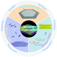
Bilayer two-dimensional (2D) single crystals have attracted intense interest due to their unprecedented properties such as van Hove singularities, superconducting state and tunable bandgap, which are exceptionally greater than those of the existing monolayer 2D materials. Accordingly, the controlled growth of bilayer domains is of great significance, where the chemical vapor deposition (CVD) approach, with the development of techniques, has become the most intuitive and flexible way to achieve this goal. Currently, numerous reports regarding the controllable modulation of the stacking structure and performance of bilayer 2D materials have been published, especially in recent decades; however, a systematic review summarizing and analyzing the state-of-the-art advances in this field is not available. Therefore, herein, we present a summary of the recent research progress on the methods and detailed strategies for the configuration modulation of bilayer 2D materials. Firstly, the general strategies for the synthesis of bilayer graphene domains are provided, highlighting the influence of the substrate, gas flow and growth pressure. Moreover, bilayer transition metal dichalcogenides (TMDs) and hexagonal boron nitride (h-BN) are listed. Thereafter, the growth mechanism of bilayer 2D single crystals is discussed in detail, taking bilayer graphene and bilayer TMD single crystals as examples. Finally, together with the development of bilayer 2D single crystals, the future research challenges towards their controllable growth and high quality and scaled synthesis are outlined, aiming to attract considerable interest in this topic.


image file: d2tc01095j-p1.tif

Dechao Geng

Dechao Geng is a full Professor at Tianjin Key Laboratory of Molecular Optoelectronic Sciences, Department of Chemistry, School of Science, Tianjin University since September 2019. Before that, he carried out research as a Research Fellow at the National University of Singapore and Singapore University of Technology and Design. He received his PhD from the Institute of Chemistry, Chinese Academy of Sciences in 2015. His current research interests mainly focus on the controlled chemical vapor deposition synthesis of 2D materials and their further properties and applications. He has published over 60 peer-reviewed articles and has served as academic editor for SmartMat.

1. Introduction

In recent years, 2D materials have attracted considerable attention in the academic and industrial field and emerged as a wealth of intriguing properties.1–5 As an essential prerequisite for these crucial properties, the controllable growth of 2D materials with well-tunable thickness has unquestionably become the desired goal of academia. At present, graphene, h-BN, and TMDs with atomically single-atom thickness exhibit amazing applications in the electronic and optical fields.6 In particular, graphene is well known for its application in gas sensors,7 corrosion-preventing agents8,9 and even energy storage devices.10 Nonetheless, the use of monolayer graphene, with an intrinsic zero-bandgap structure, is severely restricted in next-generation electronic and logic devices. Particularly, this drawback effectively limits the killer application of graphene to date. One promising route is to create bilayer graphene with a Bernal (AB)-stacked structure, which generates a tunable electronic bandgap in a vertical electric field and features more novel properties and phenomena. In contrast to bulk materials, free of dangling bonds on the surface allows the stacking of bilayer 2D materials without the limitation of lattice mismatch. Consequently, the different lattice vectors in bilayer 2D crystals lead to the formation of a superlattice or moire periodic potential.11 The majority of the novel physical performances arise from the enhancement in electronic coupling at the interface such as Mott-insulator state12 and remarkable superconductivity.13 These novel properties are sensitive to the twist angle of bilayer 2D materials such as van Hove singularities.14 Furthermore, the relative mechanism presents a new approach to modulate the properties of bilayer 2D crystals. With a variation in the interfacial twist angle, the evolution of the moire pattern introduces exotic optical, electronic and magnetic properties for condensed matter physics and practical applications. Therefore, precisely controlling the stacked structure of bilayer 2D crystals, their twist angle and even interface state is desirable in this field, allowing the controllable growth of bilayer 2D single crystals in the near future.

To date, there are three synthetic routes, which can be considered as three horse-drawn carts driving on the preparation road, each exhibiting their own merits and disadvantages (Fig. 1a). These approaches include the direct artificial stacking method,15–17 tip folding method18,19 and in situ growth strategy.20 Generally, the artificial stacking method allows the consecutive transfer of as-obtained monolayer 2D materials and their construction into bilayers or multilayers with the desired twist angles by means of an alignment transfer system. A previous report demonstrated that polydimethylsiloxane (PDMS) and an h-BN stamp could be used to tear graphene samples, which inevitably had a negative effect on the near-field interactions.21 A recent report chose a versatile pyramid stamp (PS) to assist the precise controlled stacking of bilayer graphene and had the ability to ensure its transfer on arbitrary substrates owing to the absence of h-BN.22 Finally, the organic residues were removed in chloroform and isopropyl alcohol baths. It is perceived that the stacking strategy is beneficial to obtain high-quality bilayer 2D materials by means of the typical transfer system. Meanwhile, in theory, it is versatile for the construction of stacked bilayers with desirable stacking structures for condensed matter physics studies. Of course, the inevitable residual interlayer polymer contamination leads to interfacial contaminants. A prior work addressing this problem in this field was reported by Liu's group, where they prepared twisted bilayer graphene via the layer-by-layer transfer strategy, effectively avoiding interfacial polymer contamination.16 This process is divided into three main steps (Fig. 2a). Firstly, raw graphene domains were fabricated on a Cu surface and the surface was spin-coated with poly(methyl methacrylate) (PMMA) as a protective film. Subsequently, the PMMA/graphene/substrate system was dipped in a chemical etching agent to remove the Cu substrate. After that, a transparent PMMA/graphene film was stacked on another monolayer graphene domain with a certain twist angle with the assistance of an optical microscope. Eventually, the substrate was etched again and the organic residues were removed via chemical or thermal means. Based on a series of characterizations, it was concluded that the preparation of bilayer graphene with various twist angles was successful. Meanwhile, further analysis demonstrated the absence of interfacial polymer contamination in the as-synthesized crystals, presenting a superior advancement in this field. Another success was reported by Zhang's group for the preparation of twisted bilayer MoS2.15 They used deionized water to peel off MoS2 domains and aligned them with a certain angle by virtue of a home-made alignment device (Fig. 2b and d). In summary, significant advances have been attained in manual assembly methods over the past decades, while exposing some issues such as their relative complexity and low productivity.


image file: d2tc01095j-f1.tif
Fig. 1 (a) Evaluation of three growth methods based on five aspects. (b) Atomic arrangement of bilayer graphene, h-BN and TMDs, respectively.

image file: d2tc01095j-f2.tif
Fig. 2 Twist angle engineering of bilayer 2D materials. (a) Schematic of the preparation and the corresponding band structure evolution of twisted bilayer graphene. Reproduced with permission from ref. 16. Copyright 2016, the American Chemical Society. (b) Schematic illustration of the water-assisted transfer process. (c) Atomically folding and unfolding bilayer graphene by STM tip. Reproduced with permission from ref. 18. Copyright 2019, the American Association for the Advancement of Science. (d) Various MoS2 films with precise twist angles on SiO2/Si substrate. (b and d) Reproduced with permission from ref. 15. Copyright 2020, Springer Nature.

Besides the direct stacking monolayer 2D materials, folding a continuous monolayer film through mechanical contact scribing is suitable for assembling bilayer materials. The tools for mechanical contact scribing are the tips of a scanning tunneling microscope (STM) and atomic force microscope (AFM).23 Initially, this technique was not ideal due to the weak control of the folding direction. However, in 2006, Tian and workers achieved folding and deformation using the tip of an AFM together with the symmetry of the graphite lattice.23 A central task is still to achieve precise control of the folding direction. Recently, Chen's group reported the atomically precise folding of graphene nanoislands along arbitrary orientations through STM manipulation, similar to the traditional ancient art of paper origami (Fig. 2c).18 Specifically, the twist angle of bilayer graphene could be widely tuned and the quality of the bilayer graphene was not destroyed even after folding and unfolding repeatedly. By moving the STM tip along a predetermined direction, it can generate bilayer graphene with various features and knotty twist angles in the range of 60° with an accuracy of 0.1°. However, the twist angle of folding 2D materials in some cases is largely limited by the scan orientation of the tip. The uniformity of the as-synthesized bilayer 2D crystals has a slight fluctuation owing to the appearance of wrinkles and blisters. Compared with the above-mentioned two methods, in situ growth methods such as the chemical vapor deposition (CVD) process exhibit much more opinions for the key factors to achieve controllable preparation. In fact, over the past few years, substantial research has been focused on the CVD approach for the synthesis of high-quality 2D materials, which unquestionably emerges as a promising strategy for future industrial production. Briefly, the key point of the CVD method depends on the fact that it can achieve the precise control of the nucleation and growth process by directly modulating the growth parameters. At present, many publications have demonstrated that the CVD method is a versatile technique for growing 2D materials with a controllable thickness, large area, stacking order and high quality.24–27 Notably, the reported size of monolayer 2D materials has reached the meter scale, providing a reference and expectation for their scaled practical production.28 In the case of the CVD process, there are several parameters that can effectively affect the final state of 2D materials, including catalyst, gas flow, growth pressure and growth duration.

Herein, we systematically summarize the recent advances in the mainstream CVD growth of bilayer 2D materials to provide detailed insight for researcher. Firstly, the recent progress in the synthesis of bilayer 2D single crystals is described, where graphene, TMDs and h-BN are listed successively (Fig. 1b). Owing to the decisive effect of catalysts, metal Cu and Cu-based alloys, they are discussed separately, in addition to the influence of oxygen, hydrogen and other factors. Currently, there are only a few reports in the literature on the growth of bilayer h-BN domains. Accordingly, emphasis is placed on the synthesis of bilayer graphene and TMD single crystals. Meanwhile, to deeply elucidate the growth process of bilayer 2D materials, the detailed growth mechanism is provided based on the synthesis of bilayer graphene domains. Lastly, several challenges confronting researchers are provided. This work aims to provide a deeper understanding of the growth behaviors and a roadmap to synthesize bilayer 2D materials with uniform thickness and better stacking orders.

2. CVD growth of bilayer 2D single crystals

The CVD strategy has attracted widespread interest for the well-controlled growth of 2D materials because it avoids tedious growth processes such as artificial methods.29 For example, numerous studies exhibited that this method has the advantages of controllable thickness, stacked structure, twist angle, scaled synthesis, etc., strongly relying on the flexible modulation of the growth parameters such as growth temperature, gas flow and growth duration.30–32 Based on these merits, in recent years, the quality and size of bilayer 2D single crystals have greatly improved. Therefore, in this section, we review the progress of the well-controllable synthesis of bilayer graphene, h-BN and TMDs, which is based on the modulation of the growth conditions.

2.1 Bilayer graphene single crystals

In the era of 2D materials, special attention has been paid to bilayer graphene, which can be seen as an available candidate to drive the development of practical applications owing to its open band gap, as evidenced by its vertical electric field. Furthermore, due to its other properties, including van Hove singularities,33,34 superconductive behaviors35 and Mott insulating state,36 it can serve as a catalyst for further exploration. Besides, it has been reported that bilayer graphene with miscellaneous twist angles generates different characters. For example, bilayer graphene with a minimum twist angle of 0.1° gives rise to different electronic states in graphene systems, demonstrating the importance of precisely controlling its twist angle.17 Among the growth conditions, the precursor mainly offers the raw materials for the growth of crystals, where methane is the most universal one. The carrier gas plays a dominant role in transporting carbon atoms or modulating the total pressure. Meanwhile, the growth substrate can mainly be classified into two groups, relying on the distinct solubility of carbon. One is Cu foil or Cu–Si alloy with low carbon solubility and the other is a substrate with higher carbon solubility, corresponding to Cu–Ni alloy. Therefore, this section mainly discusses the synthesis of bilayer graphene single crystals on a Cu substrate and Cu-based substrate with controllable growth conditions.
2.1.1 Cu catalyst. Since Cu was first chosen as the growth substrate for graphene in 2009,37 it has been an ideal candidate for synthesizing monolayer graphene due to its low cost and low carbon solubility. To date, a meter-size single-crystal graphene film was created by Liu's group, which is considered the closest industrial production.38 Although there are numerous reports demonstrating the remarkable properties of Cu substrates, a key point is the intrinsically low carbon solubility in bulk Cu, which results in the self-limited growth of graphene. Briefly, there is almost no possibility of obtaining extra graphene layers once the first graphene layer covers the whole Cu substrate. Recovering the catalyst ability of the Cu surface for the continuous decomposition of the carbon precursor is desirable for a breakthrough in growing bilayer graphene films. Thus, modifying the growth parameters is important such as the selection of a high flow of carbon precursors, the introduction of extra oxygen, increasing the partial pressure and employing other methods to achieve the growth of bilayer graphene.
2.1.1.1 Hydrogen. Nearly one decade ago, Duan et al. successfully fabricated bilayer graphene with a high H2 concentration.39 During the process, hydrogen not only acted as an etching agent to affect the ultimate morphology of graphene but also assisted the metal catalyst to facilitate the dehydrogenation of CH4. The growth of graphene is actually a balance between nucleation and etching. Therefore, they modified the H2/CH4 ratio up to 40 to terminate the coverage of the monolayer graphene film on the whole surface. The lateral extending growth of the monolayer graphene ceased and partially exposed Cu at the upstream end still enabled the decomposition of the CH4 species. As shown in the schematic diagram in Fig. 3a, the small decomposed fragments flowed upstream to downstream to achieve the continuous growth of bilayer graphene domains. Meanwhile, to increase the coverage of bilayer graphene, they turned the reaction pressure to a low level (1 mbar) in the initial stage to ensure the nucleation of bilayer graphene, and then increased the pressure to 5 mbar to accelerate the growth rate (Fig. 3b). Upon increasing the growth time, a uniform graphene film with higher coverage was obtained. The Raman spectroscopy results exhibited that the ratio of bilayer graphene was up to 99% and the AB stacking was up to 90%. The SAED patterns with the zone axis of [0001] exhibited the monocrystalline character of the bilayer graphene. Besides, dual-gate graphene devices were fabricated based on the as-obtained samples. The hole carrier mobility was estimated to be 1500–4400 cm2·V−1 s−1 and the electronic mobility 1400–3000 cm2·V−1 s−1.
image file: d2tc01095j-f3.tif
Fig. 3 Effects of the gas flow of H2 during the growth of bilayer graphene single crystals. (a) Schematic showing the growth process of bilayer graphene under a high gas flow of H2. (b) Different morphologies of bilayer graphene under different pressures. (a and b) Reproduced with permission from ref. 39. Copyright 2012, the American Chemical Society. (c) Optical micrograph of stripe patterned graphene on Cu foil. (d) Regrown patterned graphene transferred on Si/SiO2 substrate. (e) Growth mechanism of bilayer graphene by regrowth process. Reproduced with permission from ref. 40. Copyright 2018, the American Chemical Society. (f) Schematic showing the transformation from monolayer graphene to bilayer or multilayer graphene with increasing H2 pressure. Reproduced with permission from ref. 42. Copyright 2014, the American Chemical Society. (g) Edge passivation modes with low and high H2 flow rates, respectively. (h) Relative energy as a function of the twist angle in both models. (g and h) Reproduced with permission from ref. 44. Copyright 2020, the American Chemical Society.

Likewise, Hong's group achieved the selectively patterned growth of bilayer graphene via a two-step CVD method with the aid of H2.40 Initially, a mixture of gases of methane, H2 and Ar was introduced following the conventional CVD growth method. Then, combining photolithography and the oxygen etching technique, the as-obtained continuous graphene film was transformed into a strip configuration, and thus a portion of the Cu substrate was exposed in the reactive atmosphere (Fig. 3c). Regarding this as the regrowth substrate, a mixture of gases including carbon feedstock was introduced again for the second growth (Fig. 3d). In this period, the second nucleation simultaneously presented at the exposed Cu surface and was underneath the patterned graphene. Eventually, the unetched graphene area regrew into bilayer graphene and the residual exposed Cu surface was covered by monolayer graphene. It should be noted that the above-mentioned growth conditions during the regrowth procedure should be precisely controlled to avoid unwanted reactions. Especially, engineering the gas flow of H2 can achieve the conversion from monolayer to bilayer. With an extremely high gas flow of H2, the graphene edges would be passivated and detached from the Cu surface (Fig. 3e). Subsequently, the carbon species diffused underneath the existing graphene domains and the adlayer growth of graphene was achieved. This strategy has widely expanded the possibility for the synthesis of various micropatterns such as chairs and stars. AFM measurement of the as-obtained samples clearly exhibited that there were some rubbles or wrinkles on their surface.

The role of H2 was further studied by virtue of an ab initio molecular dynamics (AIMD) simulation.41 In detail, atomic H was attached to the edges of the top layer graphene, generating a gap between the Cu substrate and graphene edges to allow the growth of an adlayer. AIMD simulation indicated that the edges of C would strongly bond to the Cu surface to impede the diffusion of C without the participation of hydrogen atoms. In contrast, the presence of H atoms detached from the Cu surface favors the diffusion of C active species to the bottom of the first layer. Thereby, a bilayer graphene film was delivered by controlling the pressure of H2. Based on the theoretical reference, the bilayer graphene grew synchronously at high H2 pressure, and gratifyingly the coverage of bilayer graphene could reach up to 95% with the flow of H2 at 7 sccm. For simplicity, the graphene edges could be passivated by the metal surface or hydrogen atoms by precisely controlling the pressure of H2 (Fig. 3f).42 The graphene edges tended to be directly passivated by the Cu surface with a lower hydrogen pressure and exhibited H-terminated edges under high H2 pressure. The metal-passivated graphene edges were active to adsorb C monomers to extend the lateral growth of the first layer. In contrast, the H-terminated graphene edges were not active to absorb the C monomers, and accordingly the diffusion of these species under the graphene film to form bilayer graphene domains was favored. Benefitting from theoretical demonstrations, Li et al. proposed an unusual chemical ‘gate’ growth process to reveal the different growth rates of different layers by modulating the H2 pressure.43 H-passivated graphene edges with fewer graphene edges bonding to the Cu surface gave rise to the rapid diffusion of C atoms and the faster epitaxial growth of the bottom layer with the open ‘gate’. In contrast, the Cu-passivated graphene edges under a lower H2 pressure resulted in the opposite phenomenon with the close ‘gate’. This newly provided growth mode is expected to provide a guide for precisely controlling the size of the different layers in bilayer or multilayer 2D materials.

Besides, the concentration of H2 can affect the stacking orientations of bilayer graphene domains (Fig. 3g).44 The relative interlayer coupling interaction between the mutual graphene layers or between the graphene layer and Cu surface guides the twist angle of bilayer graphene. An increase in H2 concentration resulted in the stronger interlayer coupling of adjacent graphene layers, which caused a decrease in the twist angle. Therefore, AB stacking is the preferred structure for the H-passivated model. DFT calculations further revealed the roles played by the interaction factors between the graphene layer and Cu surface in the stacking orientations of bilayer graphene (Fig. 3h). There was a transferring tendency for the stacking orders from AB staking to more energetically favorable twisted graphene in the case of Cu-passivated edges. Based on the fundamental studies, it was reported that the AB-stacked structure accounted for 77% of the bilayer graphene. This well-developed ability is beneficial for exploring the possible applications of bilayer graphene in practical electronics.


2.1.1.2 Oxygen. The curial role of oxygen has been revealed and oxygen has been widely applied during the growth process. With the participation of oxygen, a centimeter-scale monolayer graphene film was produced as a result of the reduction in the nucleation density and activation energy of edge dehydrogenation.45 Meanwhile, the growth behavior progressively transformed from edge-attachment-limited to diffusion-limited mode.

Recently, the effect of oxygen during the growth of bilayer graphene has been deeply discussed.46,47 Ruoff's group creatively achieved the growth of half-millimeter size bilayer graphene single crystals in an oxygen-activated CVD process. An intrinsic flat Cu foil was folded into a Cu pocket and defined as interior (O-free) and exterior (O-rich) sides, respectively. After introducing CH4, the O-rich exterior surface was covered by large-area bilayer graphene domains, whereas only isolated dendritic graphene islands were observed on the O-free interior surface (Fig. 4a). The second graphene domains underneath the first graphene layer presented monocrystalline character, as revealed by low-energy electron diffraction. Careful analysis of the 2D band of Raman measurement showed that the AB-stacked structure in the bilayer graphene was over 80%, matching well with the transmission electron microscopy (TEM) results. To further confirm the effect of O atoms, the same growth conditions were introduced into the O-rich and O-free sides. The experimental results indicated that O activated the growth of the bilayer graphene domains and played an indispensable role in this process. The O atoms tended to combine with the H atoms to form a stable OH group, which made C–H bond cleavage much simpler (Fig. 4g). Therefore, the overall dehydrogenation energy of CHx dramatically decreased and C species were allowed to diffuse through the Cu pocket to nucleate the second layer (Fig. 4f). It should be noted that the interior surface of the Cu pocket had no possibility of forming bilayer graphene domains owing to the huge energy barrier without O atoms.


image file: d2tc01095j-f4.tif
Fig. 4 Growth of bilayer graphene with the participation of oxygen. (a) Morphology of graphene grown on OR-Cu(top) and OF-Cu(bottom), respectively. (b and c) Schematic diagram showing the growth mechanism of bilayer graphene under the assistance of a quartz tube. (d) Scanning electron microscopy (SEM) image of bilayer graphene domains on top-side of Cu surface. (e) Separated monolayer graphene domains occurring on the back side. (b–e) Reproduced with permission from ref. 47. Copyright 2016, Macmillan Publishers Limited. (f) Growth process of bilayer graphene on OR-Cu surface by back-diffusion mechanism. (g) Dehydrogenation energy of precursor on Cu (111), Cu (111) surface with step edges and Cu (111) with O. (a, f and g) Reproduced with permission from ref. 46. Copyright 2020, Science China Press and Springer-Verlag GmbH Germany, part of Springer Nature.

Zhu's group also proved the effect of oxygen by designing a distinctive device to grow bilayer graphene.46 Here, pre-treated quartz was placed underneath a flat Cu foil. With an increase in temperature, the flat Cu foil became soft and presented a difference in its two sides (Fig. 4b and c). After the growth process, large-area bilayer graphene domains were formed on the top side of the Cu foil and only several monolayer graphene domains were discretely distributed on the bottom of the Cu foil (Fig. 4d and e). Generally, the backside quartz provided continuous oxygen during the CVD growth process, which extremely facilitated the diffusion of C atoms in the bulk Cu. In contrast to the top side, the release of oxygen significantly suppressed the nucleation of graphene on the back side of the Cu foil. Therefore, the presence of oxygen generated a strong effect on the crystallinity of bilayer graphene.


2.1.1.3 Growth pressure. Other growth conditions empirically affect the quality and formation of bilayer graphene such as the cooling rate and system pressure.48,49 Yu et al. adapted a complex varying pressure CVD (VACVD) method for the growth of a continuous bilayer graphene film.48 Initially, Cu foil was annealed in a pure H2 atmosphere under ambient pressure to reconstruct the crystal arrangements of Cu foil. Once the annealing process ended, the pressure of the whole system was modulated to 3 Pa. Afterward, a mixture of CH4 and H2 gas was introduced for the growth of graphene, and meanwhile the total pressure stably reached the ambient condition again. With a variation in the pressure from 3 Pa to 101 kPa, the concentration of C fragments gradually increased, breaking the self-limiting growth of monolayer graphene and driving the growth of extra graphene layers. In this VPCVD process, a lower H2/CH4 flow rate ratio was more advantageous for the transformation of monolayer to bilayer patches (Fig. 5a). With the appropriate flow ratio of H2/CH4, a uniform large-area bilayer graphene film was formed. It should be noted that the VPCVD growth system was a non-equilibrium process. This system gave rise to the inhomogeneous growth of the second layer, and thus directly resulted in the random shape evolution of bilayer graphene. Raman spectra with a negligible D band proved the high quality of the as-obtained graphene (Fig. 5b). By analyzing the intensity of the 2D band and 2D/G, the successful formation of a bilayer graphene film with over 90% AB-stacked structure was demonstrated (Fig. 5c). The following TEM and select area electron diffraction (SAED) results were in good agreement with the Raman data.
image file: d2tc01095j-f5.tif
Fig. 5 Growth of bilayer graphene by controlling the growth pressure and morphology of the Cu surface. (a) SEM image of bilayer graphene patches. (b) Raman spectra of monolayer and bilayer graphene transferred onto SiO2/Si substrates. (c) Raman spectra exhibiting two different staking orders of bilayer graphene. (a–c) Reproduced with permission from ref. 48. Copyright 2016, The Royal Society of Chemistry. (d) Characterization of uniformly rough Cu surface. (e) Morphology of Cu surface after CH4-annealing. (f) As-grown bilayer graphene after 20 min. (e and f) Reproduced with permission from ref. 50. Copyright 2021, the American Chemical Society. (g) Schematic of various graphene domains with bilayer or trilayer configurations. (h) Typical optical image of bilayer graphene crystals. (i) Raman spectra of bilayer graphene single crystal at points A and B in panel (h). (g and i) Reproduced with permission from ref. 52. Copyright 2014, Wiley-VCH Verlag GmbH & Co. KGaA, Weinheim.

2.1.1.4 Morphology of Cu surface. In terms of the controlled synthesis of monolayer graphene single crystals, this can be achieved via a relatively smooth Cu surface such as the Cu (111) facet, owing to its low carbon solubility. Recently, it has been reported that bilayer graphene domains rather than monolayers prefer to grow on a rough Cu surface with several height and spacing protrusions.50 Thereby, the morphology of the Cu surface such as roughness is another essential factor in the preparation of bilayer graphene, which can affect its quality.

Generally, Cu foil tends to exhibit a smooth Cu (111) surface after annealing in an H2 atmosphere. In contrast, Cu foil is prone to presenting a rough surface when annealed in a CH4 atmosphere. Meanwhile, the height and spacing of the protrusions can be modified by varying the gas flow of the precursors and the annealing time. Thus, based on these strategies, Chee's group successfully fabricated a uniform rough Cu surface, and then synthesized a uniform and high-quality bilayer graphene film on a well-designed Cu surface.50 After electrochemical polishing measurement, the Cu foil was loaded in the CVD reaction furnace and annealed at 1000 °C under a CH4 atmosphere. The Cu surface absorbed a certain amount of carbon atoms and transformed into a mixture of Cu (111) and Cu (311) facets, becoming a uniformly rough structure (Fig. 5d). As shown in Fig. 5e, there was a large and regular facet on the Cu surface. Then, the surface continued to adsorb carbon atoms during the synthetic process to break the self-limited mode, finally forming bilayer graphene. For example, when the growth time was prolonged to 20 min, an entirely uniform bilayer layer was obtained, as shown in Fig. 5f. The assessments indicated that the as-obtained bilayer film possessed high transparency and low resistance. The intensity of the SAED patterns indicated that the coverage of AB-stacked bilayer graphene was 99%. Further exploring the reason for the high ratio of AB-stacked structure, the difference in work function between the smooth surface with (111) orientation and rough surface with (311) orientation was calculated. The result exhibited that the (311) surface provided a much more stable path than the smooth Cu (111) surface for the synthesis of bilayer graphene. Meanwhile, the energy of the shifting process from AA-stacked to AB-stacked continuously decreased and there was no energy barrier with a variation in these two stacked structures on the Cu (311) surface. Hence, the experiment and theory in this work are favorable for understanding the growth mechanism. To further determine the influence of the Cu facet, Choi et al. grew bilayer graphene on Cu (111) and Cu (311)/(110) facets, respectively.51 They observed nearly the same phenomenon as that in ref. 38.50 Bilayer graphene on smooth Cu (111) was prone to be AB-stacked with 30° twisted configurations, while they presented a small twist angle of less than 5° on the Cu (311)/(110) surface with atomic-stepped edges. DFT calculation confirmed the energetically favored small-angle twisted bilayer graphene on the Cu (311)/(110) facet. Thus, better control of the configurations of the Cu surface is desirable for fine-controlling the stacked structure of bilayer graphene.

To obtain single-crystal bilayer or trilayer graphene domains, a double annealing process was performed on Cu foil, and then a clean Cu surface mainly exhibiting Cu (111) lattice was obtained.52 During the first annealing process, the contaminations and existing sharp wrinkles were completely removed, which facilitated the formation of Cu edges. In the case of the mild second annealing process, the Cu foil was slightly preheated, retaining the as-formed Cu steps. This design ensured the generation of single-crystal graphene pyramids with preferred 0° and 30° interlayer stacking orientations. After growth, the samples were subjected to optical characterization and Raman analysis. It was found that the crystals exhibited varying sizes of monolayer, bilayer, and trilayer hexagons, and finally exhibited a pyramid structure (Fig. 5g). All the crystals nearly shared a common nucleation center and the second layer grew on top of the first layer with the preferred 0° and 30° rotation angles. The lateral dimensions of the monolayer graphene single crystals could reach up to 100 μm. The Raman spectrum demonstrated the AB-stacked structure of the as-obtained bilayer graphene (Fig. 5h and i). The negligible D peaks demonstrated the high quality of the graphene single crystals without obvious defects. Subsequently, they systematically revealed the preferred orientations of the graphene crystals on the Cu substrate and emphasized the critical role of the Cu steps.

They displayed the importance of the Cu steps during the angle preference phenomenon. In the case of the clean Cu substrate without impurities and obvious wrinkles, the Cu steps became the low-energy nucleation sites for C atoms. The microscopically straight and closed atom arrangements of the Cu edges were verified by characterization. The graphene edges were more prone to bond with the step atoms of Cu to consume their dangling bonds, and thus the strong interface bonding deeply rendered a variation in the graphene orientation with respect to the Cu (111) lattice. Consequently, the energy-preferred graphene-Cu step states affected the orientations between the graphene and Cu (111) surface, leading to the mutual orientation-preferred structures between the graphene layers. Among the formed orientations, the 0° and 30° interface configurations with straight zigzag (ZZ) and armchair (AC) edges exhibited the minimum interface energy, respectively. In the case of other angles, the interface was significantly unstable with both disordered Cu steps and highly buckled graphene edges. The same conclusion was gained based on the charge density difference among the various graphene-Cu systems. Notably, the Cu steps were not covered by the first graphene layer and were still exposed as nucleation sites for the second graphene layer. Guided by the edge-step nucleation process, the newly created graphene layers still presented the preferred 0° and 30° orientations with respect to the Cu surface.


2.1.1.5 Precursor. Besides the most ubiquitous precursor methane, the use of other carbon species such as ethanol with a higher carbon content and other elements has been reported to grow bilayer graphene. Not only the above-mentioned release of oxygen lowers the dehydrogenation energy of methane, but also generates decomposition products including H2O and H2, which can act as etching agents at high temperature.53 Consequently, the growth phenomena are different from that reported for bilayer graphene using methane as a precursor. In brief, the growth of bilayer graphene with ethanol follows a layer-by-layer epitaxial growing process. The first graphene layer conforms to the surface-mediated process and maintains self-limiting behavior for a short time. Owing to the etching effect of H2 or H2O coming from ethanol, flake substitution begins to occur as the process continues. Meanwhile, the newly introduced ethanol fragments trigger the growth of the second layer on top of the as-obtained graphene. The whole growth process till the end is accompanied by flake-by-flake substitution.

Analogous to a previous report, Wang's group reported the growth of uniform bilayer graphene film with a coverage of 90% by precisely optimizing the pressure ratio between ethanol and Ar.54 The SAED pattern showed a set of 6-fold symmetric diffraction spots, revealing the AB-stacking structure of bilayer graphene. Moreover, they further explained the second layer growth mechanism by establishing the growth configurations and conducting first-principles calculations based on the Cu (111) mode. Generally, C monomer, CH and CH2 radicals with strong binding energy facilitate the nucleation of the first layer. When the nucleation of bilayer graphene occurs, the aforementioned three radicals exhibit a lower binding energy than that for the nucleation of trilayer graphene, indicating that the growth of the second layer would occur together with the third layer. In contrast, the weakened binding strength of the CH3 radicals on the Cu/bilayer graphene layer can contribute to the nucleation of the bilayer graphene and prevent the growth of the third layer. Specifically, CH3 radicals, owing to their suitable binding energy on graphene, are the most active species to promote the growth of bilayer graphene.

Instead of adopting other precursors, recently, Chen's group reported the decaborane-assisted growth of high-quality 30° twisted bilayer graphene on Cu foil.55 Rather than a layer-by-layer growth behavior, they proposed that the growth of twisted bilayer graphene obeys a simultaneous growth mode with the assistance of decaborane, indicating that the twisted bilayer graphene synchronously grew from the nucleation seeds to millimeter-sized twisted graphene domains (Fig. 6a). There were two fascinating points in this experiment. One was the introduction of decaborane and the other was the selection of less diluted CH4. After treating the Cu substrate, decaborane was spun onto it as a catalyst for the decomposition of methane in the growth process. Both Raman spectroscopy and SEM characterization revealed the successful preparation of bilayer graphene and its high uniformity (Fig. 6b). The ingenious phenomenon was that there was no boundary between the two layers, demonstrating that the growth of the two graphene layers resulted from the same nuclei with the same growth rates. Referring to the SAED patterns, the two sets of 6-fold symmetry diffraction spots indicated the presence of 30° twisted bilayer graphene (Fig. 6c and d). To reveal the involvement of decaborane, they conducted a contrast experiment under the same parameters and found that there was no presence of bilayer graphene without decaborane. Methane was catalyzed and decomposed into carbon species with the help of hydrogen and decaborane in the initial process. Then, several as-existing active carbon species were loaded as the seeds of twisted bilayer graphene. With time, the lateral size of the twisted bilayer graphene simultaneously enlarged, and finally reached a dynamic equilibrium state. Therefore, decaborane acted as the cocatalyst for the top graphene layer, which had no direct contract with the Cu substrate, decomposing methane at the edges of the first layer of the twisted bilayer graphene. Besides, decaborane also affected the thickness and stacking order of the graphene domains. The other necessary point is the low methane content, which was conducive to forming a 30° rotational angle rather than a small twist angle. This successful work provides an extra path for the application of 30° quasicrystal twisted bilayer graphene.


image file: d2tc01095j-f6.tif
Fig. 6 Evolution of bilayer graphene single crystals via CVD process. (a) Bilayer graphene domains grown on Cu foil. (b) SEM image showing typical bilayer graphene crystal. (c and d) SAED patterns showing the same rotation angle of 30°. (a-d) Reproduced with permission from ref. 55. Copyright 2021, IOP Publishing Ltd. (e) Schematic diagram showing heterosite nucleation strategy. (f) Optical images of twisted bilayer graphene with various twist angles. (g) Optical images of twisted bilayer graphene domains. (h) HRTEM images of bilayer graphene domain with clear Moiré patterns. (i) Relationship between layers and flow rate of H2 and CH4. (e-i) Reproduced with permission from ref. 57. Copyright 2021, Springer Nature.

In the above-mentioned method for the synthesis of twisted graphene, a major obstacle is the immutable twist angle. It is well known that bilayer graphene with a 1.1° magic angle exhibits superconducting ability at a critical temperature of 1.7 K, whose properties are beyond that of existing 2D material systems.14,35 Bilayer graphene with a specific twist angle is generally synthesized via a manual restacking process such as the tear and stack method.56 In the case of the CVD growth strategy, bilayer graphene prefers to share a common nucleation site with the same surrounding microscopic environment, which unquestionably forms AB-stacked and 30° twisted configurations. Hence, there is a dilemma to fabricate bilayer graphene with varying controlled twist angles via CVD methods.

Recently, Liu's group proposed a groundbreaking heterosite nucleation method by means of the gas-flow perturbation strategy.57 Specifically, the nucleation of the second layer is fueled by suddenly increasing the flow rates of H2 and CH4 after the growth of the first layer (Fig. 6e). The sudden variation in the growth environment triggers the nucleation of the second layer near the edges of the first layer rather than the original nucleation center. Meanwhile, the gas-flow perturbation breaks the equilibrium in the intrinsic system and the growth of bilayer graphene with various twist angles, and therefore formed an overwhelming amount of AB-stacked bilayer graphene. As shown in Fig. 6f, a wide array of twisted bilayer graphene with a non-concentric nucleation structure was revealed by SEM characterization. About 86% twisted fraction in bilayer graphene was obtained, which is much higher than the fraction without the perturbation. Modulating the degree of flow perturbation resulted in the control of the different levels of nucleation center sites, thus achieving the controllable growth of bilayer graphene with various twist angles (Fig. 6g). As revealed by the high-resolution TEM (HRTEM) characterization, all the twisted bilayer graphene showed clear Moiré patterns (Fig. 6h) and the electronic carrier mobility of the twisted bilayer graphene reached 67[thin space (1/6-em)]000 cm2 V−1 s−1, which demonstrated the high quality of the bilayer graphene crystals.

The carbon labeling technique presented a better understanding of the elaborate growth mechanism. The total growth process obeyed the surface-mediated growth mechanism, where the second layer occurred under the first layer. Therefore, the Cu substrate effectively influenced the directions of the graphene domains. The significantly strong interactions between them facilitated the wide twisted distribution of bilayer graphene rather than only the AB-stacked structure. Notably, there are three key points to this success. Firstly, prohibiting the growth of the second layer before completing the growth of the first layer. Secondly, ensuring that the nucleation of the second layer initiated from the gas-flow perturbation. Thirdly, providing sufficient carbon feedstock for adlayer growth. The increasing content of CH4 and H2 was important for the nucleation and growth of bilayer graphene (Fig. 6i). Thus, this report presents potential for fabricating bilayer graphene with various twist angles via the versatile CVD method.

In summary, breaking the surface self-limiting mode opens a pathway for growing bilayer graphene on Cu substrates. Both AB-stacked and other twisted bilayer graphene have been successfully fabricated in recent years. Obviously, Cu is an appropriate substrate to grow bilayer graphene. However, there remains some challenges in this field such as studying more detailed growth mechanisms, exploring more precise control of the graphene structure and even finding simpler synthetic technology, which need to be solved in the future.

2.1.2 Cu-based binary alloy. Generally, Cu substrates, which feature self-limited growth processes and low carbon solubility, have limited application during the growth of bilayer graphene. With the development of the market and industry, high requirements have been put forward to fabricate appropriate graphene domains for various demands. For example, precise control of the number of graphene layers because it obviously affects the properties of the resulting graphene.58 In this case, alloy substrates, combining the advantages of different metal components such as Cu–Ni,59 Cu–Si60 and Cu–Co61 generates unique merits towards the synthesis of bilayer graphene single crystals.
2.1.2.1 Cu–Ni alloy. Generally, Cu–Ni alloy has been widely reported as a growth substrate for bilayer graphene in the CVD growth process. Ni substrates exhibit relatively higher carbon solubility and catalyst ability than Cu substrates.37 Accordingly, carbon monomers can adequately diffuse into the bulk Ni, and subsequently precipitate on the surface to form multilayer graphene. Furthermore, the catalytic ability of Cu–Ni alloy is indeed much better than that of pure Cu and effectively avoids the precipitation of multilayer graphene film. Consequently, based on these properties, Cu–Ni alloy correspondingly prevails in the growth process. The design of Cu–Ni alloy and the modulation of growth parameters have been drastically explored to prepare high-quality bilayer graphene single crystals. Thus, here, we summarize the tremendous advances in this field.
2.1.2.1.1 Ni content in Cu–Ni alloy. Firstly, to ensure the homogenous surface morphology of graphene, depositing Cu after Ni is more conductive than the opposite deposition sequence for the fabrication of Cu–Ni substrates.62 Ago et al. substantiated that lots of Ni atoms will dissolve in bulk Cu to replace Cu atoms at a high processing temperature, accordingly leading to the formation of a very rough surface. However, a rough surface inevitably results in the degradation of the quality of graphene.

The Cu/Ni ratio of the bulk alloy is always a promising solution to control the growth of graphene given that it closely affects the coverage and layers of single crystals. In this regard, an increase in the concentration of Ni results in the generation of bilayer or even multilayer graphene. Recently, Ruoff's group creatively established a correlation between the Ni concentration and graphene layers.63 Specifically, by heating Ni-plated Cu (111) foil, a set of monocrystalline Cu/Ni (111) foils was obtained, whose Ni content could be regulated by adjusting the amount of Ni coating (Fig. 7a). In addition, the design of a single-crystal Cu–Ni alloy, thoroughly avoiding the interaction between graphene and impurities, ensured the high quality of the bilayer graphene domains. Initially, an Ni film was plated onto both sides of a Cu (111) surface and thermally treated to obtain Cu–Ni alloy. The Cu–Ni alloy presented a well monocrystalline character, as revealed by EBSD maps and XRD patterns.


image file: d2tc01095j-f7.tif
Fig. 7 Synthesis of bilayer graphene on monocrystalline Cu–Ni alloy. (a) Schematic of preparation of single-crystalline Cu–Ni alloy. (b) Optical images of bilayer graphene islands, bilayer film and trilayer graphene. (c) Raman spectra showing monolayer, AB-stacked bilayer and ABA-stacked trilayer graphene. (d) Stress-strain responses for 260[thin space (1/6-em)]nm PC and 260[thin space (1/6-em)]nm PC-bilayer graphene film, respectively. Reproduced with permission from ref. 63. Copyright 2020, Springer Nature.

After introducing methane with a gas flow of 1 sscm at 1075 °C, large-area AB-stacked bilayer graphene single crystals were eventually obtained on the Cu–Ni alloy substrate (16.6 at%) (Fig. 7b). The morphology of graphene tended to be monolayer in the case of an Ni concentration of 10.2 at%. The growth behaviors presented high resemblance with the growth process on the Cu surface. A further increase in the Ni content (12.9 at%) resulted in the emergence of bilayer graphene domains. Besides, the coverage of bilayer graphene increased as the ratio of Ni varied from 12.9 at% to 16.6 at%. The Ni content in the Cu–Ni alloy gradually increased up to 18.2 at%, where high amounts of carbon atoms segregated at the interface, inducing the formation of trilayer graphene single crystals (Fig. 7c). The TEM studies demonstrated the “inverted wedding cake” structure of the bilayer graphene single crystals, indicating that the second small layer was under the top continuous film. The performance of the dual-gate graphene transport device demonstrated the tunability of the bandgap in bilayer graphene. By employing a polycarbonate film as a support, the average Young's modulus of polycarbonate-bilayer graphene was determined to be about 3.48 GPa owing to its superior properties compared that in other reports (Fig. 7d). Based on fundamental experiments, they further speculated the elaborate segregation-dominated growth mechanism by virtue of the ToF-SIMS technique and hydrogen etching phenomena. This method advances the scaled production of bilayer graphene via the CVD approach.


2.1.2.1.2 The design of Cu–Ni alloy. Several novel experimental techniques have recently emerged for the growth of bilayer graphene on Cu–Ni binary substrates. Yoo's team proposed the fabrication of an asymmetric Cu catalyst by depositing Ni film on the back side of a partial Cu film to break the carbon solubility symmetry in Cu foils, which was effective for the growth of bilayer graphene.64 Furthermore, simply regulating the thickness of the deposited Ni film could change the number of layers of as-grown graphene. Wafer-scale AB-stacked multilayer graphene was produced with an Ni film at a thickness of 200 nm. Further characterization of the as-grown bilayer graphene showed that it exhibited a low Rs at the same transmittance and high quality with nearly negligible defects.

In recent years, Ni–Cu gradient alloy has been designed to synthesize large-size bilayer graphene single crystals. In 2018, Gao et al. reported the preparation of bilayer graphene crystals with a lateral size of up to 200 μm on an Ni–Cu gradient alloy (Fig. 8a).65 The Ni–Cu gradient alloy was fabricated by annealing Cu foil with Ni film sputtering on the one side at 1050 °C for 5 min. The Ni atoms gradually distributed to form a Ni-rich side and Ni-poor side, respectively. Due to the high catalyst ability of the Ni metal, the first layer of graphene grew on the Ni-rich surface initially, whereas only a small proportion monolayer was formed on the Ni-poor surface (Fig. 8b). With an increase in the reaction time, the carbon diffused from the Ni-poor side to the Ni-rich side through a carbon back-diffusion manner, similar to the previous report. This approach mainly relies on the different concentrations on the two sides of the Ni layer. ToF-SIMS showed that the concentration of the Ni-rich surface was 20 times higher than that in the other side, and thus the graphene growth ratio on the Ni-rich surface and Ni-poor surface was 100%/18%. The main contribution of this strategy is the production of high-crystalline bilayer graphene and uniform sizes of as-obtained bilayer graphene domains. Raman spectra demonstrated the presence of two configurations, i.e., AB-stacked structure and 30° twisted bilayer graphene.


image file: d2tc01095j-f8.tif
Fig. 8 Preparation of bilayer graphene on Ni–Cu gradient alloy. (a) Schematic diagram showing the process for the preparation of the Ni–Cu gradient alloy and growth process of bilayer graphene. (b) Optical images revealing the morphology of graphene on the Ni-rich side and Ni-poor side, respectively. Reproduced with permission from ref. 65. Copyright 2018, the American Chemical Society. (c) STM images of bilayer graphene after 10 h CVD growth process. The insert is the corresponding FFT pattern. (d) STEM image showing perfect AB-stacked structure of bilayer graphene. (e) Evolution of the coverage and the ratio of AB-staked structure varying with CVD growth time. Reproduced with permission from ref. 66. Copyright 2020, the American Chemical Society. (f) Schematic illustration of the growth behaviors of trilayer graphene in Ni–Cu gradient alloy. (g) Schematic of the relationship among the substrate curvature, interlayer interaction and in-plane strain. Reproduced with permission from ref. 43. Copyright 2020, The Author(s). Springer Nature.

The gradient Ni–Cu alloy is not only suitable for the growth of AB-stacked bilayer graphene single crystals, but also allows the controllable synthesis of trilayer graphene, as reported. Two years later, Gao and colleagues creatively reported the successful synthesis of trilayer graphene with controllable ABC yields (Fig. 8f).43 The key insight was the emerging substrate topography, which improved the stability of the ABC structure. Specifically, there was a quasi-periodic pattern with strikingly different curvatures, which introduced in-plane interlayer strain, affecting the atomic registry between two adjacent layers. Thus, a structural transformation between ABC and ABA directly occurred with the dislocation formation. With the aid of DFT calculations, they concluded that the curvature of the Ni–Cu surface resulted in the appearance of interlayer dislocations, consequently ensuring the existence of ABC domains (Fig. 8g). For example, large ABC domains with z-R22R interfaces could stably exist on the substrate with appropriate surface curvatures. After being transferred onto an Si/SiO2 substrate, trilayer graphene with both ABC and ABA configurations presented enlarged lateral dimensions owing to the disappearance of interlayer dislocation pairs on the flat surface.

In addition to the characteristics of the Cu–Ni alloy, other parameters such as the growth duration are effective candidates for controlling of the stacked structure of bilayer graphene domains. According to theory, AB-stacked bilayer graphene is the most stable state on Cu–Ni alloy, which is analogous with Cu as a growth substrate, while 30° twisted bilayer graphene is frequently accompanied with the AB-stacked structure during the growth process.62 Meanwhile, bilayer graphene with a 30° twist angle is preferably formed on the Cu–Ni alloy than the Cu surface. Thus, to resolve the mixed stacked structure of bilayer graphene, Ago et al. found that a gradual transformation occurs for the stacked structure of bilayer graphene, whose structure is prone to only the AB-stacked structure with an elongation of the CVD growth process.66 They synthesized bilayer graphene at a high temperature on a high Ni ratio of Cu–Ni alloy with a rapid growth rate. These growth conditions greatly benefited the isothermal segregation of bilayer graphene. After the growth process was complete, the system was cooled to room temperature quickly to prevent the formation of unwanted products. The STM image and high-resolution STEM image taken of the samples evidenced the AB stacking structure of the bilayer graphene domains (Fig. 8c and d), respectively. As shown in Fig. 8e, the proportion of bilayer graphene reached up to 93% after 10 min reaction, which highlights the efficiency of this method. Subsequently, there was a direct trend of an increasing amount of bilayer graphene with AB-stacked configuration upon extending the CVD growth time. Eventually, the ratio of AB-stacked bilayer graphene approached 99.4% after 10 h. However, it should be noted that the coverage of bilayer graphene after 10 h growth did not decrease and a 5 × 3 cm2 bilayer graphene film was obtained. The specific growth mechanism includes two stages, i.e., surface-mediated process and isothermal segregation process. CH4 was labeled with 12CH4 and 13CH4 species and Raman characterization conducted under three experimental growth conditions. According to the Raman spectra for the different growth conditions, bilayer graphene was formed in the first 30 min, while it underwent a structural reconstruction when twisted bilayer graphene transformed into AB-stacked bilayer graphene. Notably, there were no exchanged carbon atoms in this process. The first graphene layer was formed via surface processes with a high carbon concentration and high growth temperature. With an increment in the carbon content, isothermal segregation began to promote the growth of the adlayer under the first layer. The growth of the two layers finished once the Cu–Ni alloy was completely covered by graphene. Next, the second layer of twisted bilayer graphene had a tendency to be re-dissolved in the Cu–Ni bulk and sequentially resegregated to form an AB-stacked structure, which was the most energetically favored state. Consequently, the ratio of AB-stacked configuration gradually increased and bilayer graphene with other twist angles became negligible with time. Likewise, the continuous supply of CH4 assisted the reconstruction behaviors of bilayer graphene by suppressing the evaporation of carbon atoms and H2 etching at high temperature. The above-mentioned approach is suitable for the scaled production of high-ratio AB-stacked bilayer graphene.

Overall, based on the above-mentioned typical advances, the control of the Ni content in the Cu–Ni alloy for the creation of graphene domains is the key point in this system. High-quality, large-area bilayer graphene can be realized, accompanied by the regulation of other parameters. Therefore, Cu–Ni alloy is very suitable for the ultimate commercialization industry goal, together with the roll-to-roll or batch-to-batch production method.


2.1.2.2 Cu–Si alloy. Recently, significant process has been made in the fabrication of highly uniform bilayer graphene or trilayer graphene without mixtures in the graphene layer. In 2020, Lee's group creatively achieved the regulation of layers and stacked structure of a monocrystalline graphene film on Cu–Si alloy.60 The formation of SiC was considered to be a critical factor in the controlled growth of graphene. Overall, four steps were included during the synthesis process (Fig. 9a). Firstly, Cu–Si alloy was formed by annealing Cu foil at 900 °C in an H2-rich atmosphere. Subsequently, methane was introduced in the furnace, resulting in the synthesis of SiC. Subsequently, the flow of methane was stopped and the temperature of the system was elevated to 1075 °C. The high temperature led to the cleavage of the preformed Si-C bonds and the sublimation of the Si atoms. The C atoms were reserved to act as the nucleation sites of bilayer or multilayer graphene and extend to single crystals during this process. Finally, the whole SiC film was converted into graphene domains, stitching together to form a continuous graphene film.
image file: d2tc01095j-f9.tif
Fig. 9 Fabrication of bilayer graphene with Cu-based binary metal as substrate. (a) Evolution of bilayer graphene on Cu-Si alloy. (b) Morphology of graphene on Cu-Si substrate with different Si contents. (a and b) Reproduced with permission from ref. 60. Copyright 2020, Springer Nature. (c) Raman mapping showing good uniformity and high quality of AB-stacked bilayer graphene. Reproduced with permission from ref. 61. Copyright 2013, The Royal Society of Chemistry.

Besides, both the Si content and methane concentration had an effect on the thickness of the graphene domains. A small content of Si atoms tended to result in a random non-uniform graphene thickness, while a much higher Si content in the Cu–Si alloy severely limited the growth of graphene owing to the decreased catalytic ability of the Cu surface (Fig. 9b). Based on this conclusion, methane at 0.03% content was employed for the growth of bilayer graphene with a fixed Si concentration (28.7 at%). The 2D bands in the Raman spectrum of the bilayer graphene showed nearly identical line shapes with that of the exfoliated graphene, confirming the presence of the AB-stacked structure. Further performing statistical calculations, it was shown that the bilayer graphene exhibited 100% AB stacked structure and there was no other stacked orders for the trilayer graphene as well. This approach is also generally suitable for the regulation of the layer numbers in other 2D materials.


2.1.2.3 Cu–Co alloy. In addition to Cu–Si alloy, Co–Cu alloy is also a promising candidate for controlling the layer numbers and the stacked orders of bilayer graphene. In the case of pure Co, it possess the minimum lattice mismatch with graphene and its d-states show strong electronic coupling with the graphene π-states, which are conducive for the synthesis of graphene. Nevertheless, graphene grown on Co substrates generally showed a mixture of multilayer morphology. Jiang et al. synthesized Co–Cu alloy to achieve controlled layers of graphene domains.61 The fabrication process of the Co–Cu alloy is similar to that of the Cu–Ni alloy, in which a Co thin film was deposited on Cu foil by radio frequency sputtering. Uniform graphene with controlled layers could be synthesized on its surface. The number of graphene layers was significantly dependent on the thickness of the Co thin film. Bilayer graphene tended to grow on the 80 nm Co layer. Raman mapping gave clear evidence that the coverage of bilayer graphene was 99% (Fig. 9c). The excellent optical transmittance characters and electrical properties classified the as-obtained graphene among the best ranking to date. Besides, employing 80 nm and 205 nm Co thin films resulted in the formation of monolayer and trilayer graphene, respectively.

The growth mechanism is distinctly different from that of surface-mediated or precipitation processes in traditional transition metal binary alloys. It is interesting to understand the self-regulating role of the Co atoms in this synthesis process. Initially, methane precursor is catalyzed by the top Co layer. The active carbon species prefer to dissolve in the Co layer due to its high carbon solubility. Meanwhile, the Cu atoms tend to diffuse to the Co atoms via lattice vacancies. Notably, the diffusion rate of C atoms is faster than that of Cu atoms. With an elongation of the growth time, the diffusion of Cu atoms into the Co layers causes the C atoms to segregate out from the Co–Cu alloy surface, eventually forming bilayer or multilayer graphene. Overall, the Co layer acts as a higher carbon capture layer and the inter-diffusion of Cu atoms reduces the solubility of Co, driving the segregation of C atoms to form graphene.

Briefly, CVD, as an easy-to-understand approach, exhibits a large reversible capacity and high flexibility in growth of bilayer 2D materials. There are many degrees of freedom available for controlling the stacking orders, crystalline quality and lateral size, including selection of the growth substrate, introduction of oxygen, variation of the growth temperature and modulation of the total pressure. In parallel with the summary of the abovementioned current advances, the detailed procedures for the controllable synthesis of bilayer graphene domains or films on Cu and Cu-based alloy are provided in Table 1, aiming to stimulate more research in this field.

Table 1 Summary of the CVD growth process and properties of bilayer graphene domains
Substrate Method Precursor Temp. (°C) Press. Time (min) Key points Domain size Performance (cm2 V−1 s−1) Ref.
Cu LPCVD CH4 1050 5 mbar 60 (a) Two-step CVD process μm scale 4400 (RT) 39
(b) High H2/CH4 ratio
APCVD Acetone 1040 AP 60 Softening Cu foil on quartz to ensure a difference on both sides. 16 cm2 (Film) 6790 (RT) 46
CVD CH4 1000 0.1 Torr (a) Oxygen-activated CVD process 300–550 μm 60000 (1.7 K) 47
(b) Cu-pocket 20000 (300 K)
VPCVD CH4 1020 3 Pa–101 kPa 21 Varied pressure CVD process μm scale 48
CVD CH4 1000 0.5 Torr 15 First synthesis of wafer-scale bilayer graphene film 2in.× 2in. (Film) 580 (RT) 49
LPCVD CH4 1000 1.5 Torr 10–30 CH4 annealing of Cu foil to form a uniform rough surface 4 cm2 (Film) 1000–2000 50
ACCVD Ethanol 1000 50 Pa 90 Alcohol catalytic CVD process μm scale 53
LPCVD Ethanol 1000 3 Pa 180 Carefully adjusting flow rate of ethanol μm scale 54
CVD CH4 1050 Decaborane assisting synchronous growth on Cu foil 1200 μm 3671.3 55
LPCVD CH4 1020 15 Heterosite nucleation strategy μm scale 68000 (RT) 57
CVD CH4 1070 1–1000 mbar 5–20 Maintaining a catalytic inactive Cu2O layer 300 μm 16[thin space (1/6-em)]000 67
LPCVD CH4 1030 500 Pa 20–30 μm scale 68
Cu–Ni alloy CVD CH4 920 0.1 mbar 120 s (a) Tuning the partial pressure of CH4 30–60 μm > 3 in. × 3 in. (Film) 3450 59
(b) Providing sufficient carbon atoms
(c) Controlling Cu/Ni ratio
APCVD CH4 1075 AP 30 (a) Adopting low cooling process μm scale 62
(b) Ni concentration at 22%
(c) Depositing Ni followed by Cu
CVD CH4 1075 40 Torr (a) Single-crystal Cu–Ni alloy μm scale Thermal conductivity 2300 W m−1 K−1 63
(b) Ni content at 16.6 at%
CVD CH4 1000 120 Depositing 200 nm Ni onto the half of back of a Cu foil μm scale R S = 200 Ω sq−1 64
APCVD CH4 1050 AP (a) Cu–Ni gradient alloy 200 ± 50 μm 2700 ± 400 (VBG = 0V) 65
(b) 160 nm Ni on 25 μm thick Cu sheet
Cu–Ni film CVD CH4 1085 10 min–10 h (a) Extending growth time 15 cm2 (Film) 910 66
(b) Ni content at 23%
Cu–Si alloy APCVD CH4 1075 AP 10 (a) Si composition at 28.7 at% μm scale 60
(b) CH4 concentrations at 0.03%
Cu–Co alloy APCVD CH4 850–1050 AP 5–20 80 nm-Co-coated Cu foil μm scale 836.4 RS = 624 Ω sq−1 61


2.2 Bilayer TMD single crystals

As an indispensable member of the 2D material family and the perfect partner to graphene, TMDs have gradually become a research hotspot,69,70 which usually consist of transition metal elements such as Mo, W, and V and chalcogen atoms including S and Se.71 2D TMDs have a distinct structure from graphene, where the transition metal atoms interact with the in-plane chalcogen via strong covalent bonds, forming sandwiched structures.72 In sharp contrast with the rigid covalent interaction, the interaction between neighboring layers is demonstrated to be van der Waals (VdWs) force, allowing the exploration of the properties of bilayer or multilayer TMDs.73 Meanwhile, this unique configuration offers an extra degree of freedom to understand and modulate the original stacking orders of bilayer TMDs, aiming to achieve their expansive applications. To the best of our knowledge, monolayer TMDs exhibit lower carrier mobility, resulting from the scattering of interface impurities. However, bilayer TMDs, owning their interlayer coupling and charge screening, generate more intriguing performances, emerging as a promising candidate in the family of 2D materials.74,75 The development of bilayer TMDs not only stimulates competitive applications in the field of phototransistors,76 photodetectros,77 solar cells,78,79 and light-emitting diodes (LED),80–82 but also provides a possible platform to study fundamental physical properties.83–85

In the case of the CVD growth conditions for TMDs, Cu and Ni catalysts are not desirable owing to the presence of the S element. Therefore, the growth of bilayer TMDs on SiO2/Si, sapphire,86 mica and even Au substrates will be elaborated in this review. Besides the substrate, the precursor state, growth temperature, and gas flow of H2 have an influence on the growth process of bilayer TMDs. Here, in this part, we systematically provide an update-to-date summary of the recent advances in bilayer TMDs.

2.2.1 Growth precursors. There are two promising strategies to precisely control the growth of bilayer TMDs, involving stability and concentration. A detailed discussion is provided as follows. Firstly, in the case of the generally employed solid precursors, a crucial problem is the control of extra vapor pressure and the vapor elemental composition. In particular, the growth behaviors of solid pressure will gradually vary with the growth time, presenting a great challenge in the controlled growth of bilayer TMDs in terms of lateral size and layer numbers. Thus, great efforts have been devoted to alleviating these phenomena.

Recently, Duan and colleagues explored a procedure that introduced a pre-annealing step in a reverse flow before the extra nucleation and growth steps.87 The reverse flow, as shown in Fig. 10a, flowed from the substrate to the precursor, which was conducive to avoid unnecessary gas-phase reactants. A pre-annealing process was performed on the precursor at 1120 °C for 30 min. Subsequently, the gas flow was immediately switched to the forward direction for the growth of a uniform bilayer WSe2 film. Highly ultra-uniform WSe2 single crystals with controlled layers were achieved, whereas the WSe2 domains featured a mixed layer thickness and random lateral size without the pre-annealing process (Fig. 10b). Meanwhile, the high temperature not only facilitated the evaporation of the precursors and the growth rate of the domains but also promoted the atomic migration on the substrate, and further gave rise to the rapid growth of the domains. Further in-depth exploration revealed that the morphology and composition of the solid precursors changed with an increase in the processing duration. On the one hand, the proportion of small particles decreased from 90% to 40% after 60 min pre-annealing process (Fig. 10c). On the other hand, the atom ratio of Se/W significantly decreased as the pre-annealing duration increased, which was mainly attributed to the faster volatility of the Se element (Fig. 10d). This atom ratio, minimizing the poorly controlled Se elements, was effective to guarantee a stable supply of reactive vapor and conducive to the precise control of the layer thickness. Therefore, homogeneous bilayer WSe2 single crystals were obtained with a pre-annealing time of 30 min and monolayer WSe2 single crystals with a uniform growth rate and thickness were obtained with a longer pre-annealing time. The atomic-resolution STEM characterization of the bilayer WSe2 indicated the presence of AA′ stacking in the WSe2 single crystal, similar to the results revealed by the FFT pattern. After 5 min growth, the lateral size of the bilayer WSe2 film reached up to 600 μm. The FET devices based on the bilayer WSe2 single crystals exhibited the highest mobility of up to 145 cm2 V−1 s−1, which is the best value to date. Recently, Huang et al. chose WO3 film arrays as growth precursors, which were predeposited on the substrate by thermal evaporation, achieving large-area high-quality homogeneous TMD crystals.88 The content of WO3 could be precisely controlled by varying the thickness and size of the WO3 arrays. Meanwhile, H2S gas as the S source was transferred by Ar to the reaction zone. With the ability to precisely modulate the precursors and the ratio of W/S, it was observed that there was a typical U-type relationship between the layer number and W/S ratio. This indicates that a low W/S ratio significantly promoted the growth of multilayer WS2 domains and the number of layers gradually decreased with an increase in the W/S ratio. Further calculations revealed that the W/S ratio directly affected the competition between the growth of the domains along the lateral and vertical directions. Consequently, pure WS2 crystals with a controllable monolayer, bilayer or trilayer could be obtained on the substrate. This general strategy offers a pathway to mediate the metal/chalcogenide ratio to achieve wafer-scale monocrystalline TMD films for further exploring their practical applications.


image file: d2tc01095j-f10.tif
Fig. 10 Treatment of the precursor to obtain bilayer TMD crystals. (a) Schematic illustration showing gas flow with forward and reverse directions. (b) Optical images showing different structures of the as-grown WSe2 crystals with different annealing times. The scale bars are 100 μm. (c) Effect of annealing treatment on the solid source materials. The scale bars are 10 μm. (d) Atom ratio of Se/W as a function of annealing time. (a–d) Reproduced with permission from ref. 87. Copyright 2021, the American Chemical Society. (e) Fan-like morphology of as-obtained WS2. (f) Optical images of as-grown WS2 with the various contents of WO3. (g) Average areal ratio of bilayer to monolayer increasing with the volume of WO3 solution. (e-g) Reproduced with permission from ref. 89. Copyright 2021, Elsevier B.V.

Alternatively, solution or aqueous precursors have also been employed for the growth of uniform bilayer TMD single crystals. Balakrishnan et al. chose as-synthesized aqueous WO3 nanorods and S powder as the precursors for the controlled growth of bilayer WS2 domains.89 The morphology and evolution of the WS2 domains varied with the content of WO3 nanorods, allowing the growth of bilayer and trilayer structures. It should be note that the morphology of the bilayer WS2 presented a fan-like structure, where three facets presented a bilayer and the remaining facets remained uncovered. That indicated that the bilayer and trilayer WS2 selectively grew on the substrate owing to the difference in the luminescent facets. In detail, the growth of the first layer obeyed a hexagonal manner, namely two different sets of arrangements in the six facets in each WS2 domain (Fig. 10e). In addition, further observing the growth behaviors of WS2 under different concentrations of WO3 (Fig. 10f), as shown in Fig. 10g, there was a direct trend of the layers of WS2 increasing with an increase in the dispersion volume, and the areal coverage of bilayer WS2 also monotonically increase as a function of the WO3 content. One of the regions transformed to a bilayer structure with the volume of 200 μL. Thus, the use of a liquid precursor is suitable for the regulation of the quality, size and thickness of the samples. Yan et al. employed aqueous ammonium molybdate with a volume of 4 mL, 5 mL and 6 mL spun on an Si surface to synthesize MoS2 single crystals with a specific thickness.90 Overall, solution precursors are effective to control the thickness and uniformity of bilayer 2D materials.

Regarding the content of the precursors, the coverage and growth mechanism depend on the concentration of the source. In general, the initial nucleation of the second layer materials begins at the center of the first layer, which also inevitably leads to the exposure of the bottom layer. Li and co-workers reported the growth of bilayer MoS2 crystals with complete coverage of the top layer.91 Specifically, a novel device used to ensure that the high concentration of Mo source was designed, where MoS3 powder was loaded in a tube with a small vent hole. This ensured the high concentration of Mo source in the growth system by confining the precursor flow to only one direction. Meanwhile, the glass substrate was placed very close to the MoO3 powder and kept a certain distance from the S source. The well-designed CVD system created an Mo-rich edge for the growth of bilayer MoS2. Specifically, the Mo-rich edge acted as the nucleation site of the second layer and gradually grew horizontally from the edges to the center of the monolayer MoS2 (Fig. 11a and b). This unique growth process ensured the formation of bilayer MoS2 with the two layers possessing the same size. As revealed by optical images, the lateral size of the bilayer MoS2 crystals was approximately 35 μm. The high quality and uniform thickness were substantiated by a series of AFM images.


image file: d2tc01095j-f11.tif
Fig. 11 Growth process of bilayer TMD single crystals. (a) Growth process of the second layer of MoS2 based on different concentrations of Mo source. (b) Evolution of bilayer MoS2 from the edges of monolayer MoS2. (a and b) Reproduced with permission from ref. 91. Copyright 2021, Elsevier Ltd and Techna Group S.r.l, respectively. (c) Deposition of carbon nanoparticles on a sapphire substrate. (d) Bilayer WS2 with homogeneous thickness. (c and d) Reproduced with permission from ref. 95. Copyright 2019, Springer Nature. Weinheim.

Finally, it was reported that introducing extra aromatic molecules is viable for homogeneous nucleation, such as PMMA, perylene-3,4,9,10-tetracarboxylic acid tetrapotassium salt, and reduced graphene oxide.92–94 Based on this strategy, Huang et al. successfully fabricated high-quality WS2 by means of carbon nanoparticles.95 Initially, a burning candle was placed underneath a sapphire substrate, where the concentration of carbon nanoparticles could be regulated by the burning time (Fig. 11c). With this as the substrate, the solid precursors were heated at 350 °C and 1000 °C, respectively, in a double-zone CVD growth furnace. After maintaining the growth time for 10 min, bilayer WS2 domains with a lateral size on the mm-scale could be synthesized. During this process, the carbon nanoparticles reached the surface of the sapphire and facilitated the generation of intermediate WO3−x. The size of the carbon particles decreased with an increment in the WO3 vapor. WO3−x had a tendency to gather around the carbon particles, and thus resulted in a locally high concentration of WO3−x. Then, S reacted with WO3−x and formed bilayer WS2 domains. Overall, it is necessary to understand the roles of the carbon particles in the growth process, including enhancing the adsorption of WO3, facilitating the generation of WO3−x, and providing nucleation sites for bilayer WS2. As shown in Fig. 11d, the as-obtained triangular bilayer WS2 possessed a homogeneous thickness, in which the surface was flat and the edges were sharp. HRTEM revealed the high crystallinity of the bilayer graphene domains. AFM and Raman spectra were used to determine the thickness of the samples. The as-fabricated bilayer WS2 FET exhibited a mobility of 34 cm2 V−1 s−1, which is higher than that of monolayer WS2 in the present work.

2.2.2 The growth temperature. Although intense efforts have been made, control of the stacking order of bilayer TMDs remains a challenge, where bilayer TMD crystals usually presented a mixture of AB and AB′-stacking. The AB-stacked configuration is the most frequent and stable state because of its shortest interlayer space and strongest interlayer coupling. In addition, as-obtained bilayer TMDs generally include mixed monolayer, bilayer and even trilayer regions. This results in a decrease in film quality and not suitable for integration in electronic devices. Among the growth parameters, the growth temperature is significant in the regulation of the stacked structure of bilayer TMDs. For example, Pan's group demonstrated a temperature-selective physical vapor deposition trend that triangular 3R-phase WS2 crystals were largely distributed on the substrate when the temperature was 1140 °C, whereas hexagon-shaped 2H-phase WS2 domains occurred at a temperature of around 950 °C.96 In another example, Gao and co-workers creatively achieved the growth of bilayer MoS2 with an identical AB-stacked structure, which required a high-growth temperature in the synthesis process.97 The elevated growth temperature (900 °C) enabled the regulation of the nucleation and extension of the second layer in a stable growth environment. The SEM and photoemission electron microscopy (PEEM) images demonstrated bilayer MoS2 single crystals featuring a coinciding AB-stacked order without the presence of other configurations. This approach creates a new avenue for the controlled synthesis of bilayer TMDs by varying the temperature.

With further exploration, two years ago, Zhang et al. achieved the epitaxial growth of completely bilayer MoS2 single crystals in a customized temperature system, together with a reverse hydrogen flow, via a two-stage CVD growth method.98 As shown in Fig. 12a, the growth process follows two stages, including A–B stages and C–D stages, representing the growth process of monolayer MoS2 and bilayer MoS2, respectively. It was found that a customized temperature at 700 °C was appropriate to synthesize the first monolayer crystals, while a higher temperature was beneficial for the growth of bilayer MoS2 crystals because a high temperature (e.g., 750 °C or 800 °C) prevented the lateral epitaxial growth at the edges of the monolayer domains. The growth temperature also determined the stacked structures, wherein 750 °C favored the growth of the AA-stacked structure, while 800 °C was optimal for the AB-stacked structure (Fig. 12b). Besides, a reverse hydrogen flow was introduced in the system at the swing stage (B–C stage). As mentioned above, the reverse hydrogen flow provided significant benefits in preventing the formation of randomly distributed monolayer MoS2 domains and undesirable new nucleation centers. The reverse gas flow resulted in the nucleation of the second layer over the as-obtained MoS2 from the original nucleation centers. As revealed by the optical images, triangles and hexagons were the dominant shapes of the bilayer MoS2 crystals. The lateral size of the complete bilayer MoS2 single crystal was up to 300 μm. The TEM images showed a well-aligned honeycomb lattice, further indicating the high-quality single-crystalline nature of the samples. This approach is robust for the growth of other bilayer TMDs, ternary alloys and quaternary alloys, simply by choosing the corresponding precursors and optimizing the growth temperature.


image file: d2tc01095j-f12.tif
Fig. 12 Precise control of the growth of bilayer TMD single crystals. (a) Schematic diagram of the growth of bilayer MoS2 in a customized temperature system. (b) AA-stacked bilayer (hexagon) MoS2 (top) and AB-stacking (triangle) bilayer MoS2 samples (bottom). (a and b) Reproduced with permission from ref. 98. Copyright 2019, Springer Nature. (c) Optical images of twisted bilayer WS2. Reproduced with permission from ref. 99. Copyright 2015, WILEY-VCH Verlag GmbH & Co. KGaA, Weinheim.

In the case of bilayer WS2, Fan et al. synthesized a series of twisted WS2 bilayers, such as 0°, 13°, and 30° at a well-regulated temperature via the CVD method (Fig. 12c).99 It was found that bilayer WS2 with an AA or AB-stacked order was prone to occur at a lower temperature of about 850 °C, while the stacked orders preferred to be random at high temperature because the high temperature gave the driving force to overcome the angle mismatch between adjacent layers. Subsequently, further exploration of the unique structure of bilayer WS2 was conducted. The twisted bilayer WS2 exhibited weakened interlayer coupling due to its larger interlayer space than that of the AA or AB-stacked structure. The photoluminescence curves showed the absence of an indirect transition peak, indicating the direct bandgap structure of the twisted bilayer WS2, which is different from the AA and AB-stacked bilayer WS2 with an indirect bandgap. Thus, twisted bilayer WS2 can be considered as a quasi-direct bandgap material owing to its weakened interlayer coupling.

2.2.3 Hydrogen. As an imperative factor in the growth of bilayer TMDs, precise control of the content of hydrogen has attracted intense interest. According to previous reports, the lateral size of TMDs usually increases with an increase in the pressure of the chalcogen precursor. Therefore, it is of great importance to increase the content of chalcogen atoms and the intermediate phase, wherein H2 is beneficial for the formation of intermediate phases and is indirectly conducive for the preparation of large-area bilayer TMD single crystals. Taking MoS2 as an example, previous reports claimed that the presence of H2 prohibited the lateral growth of the first MoS2 flakes, thus leading to the evolution of a bilayer structure in 2D materials.98 Zhang's group further reported the in-depth exploration of the role of H2 in the growth process. They concluded that the relatively high gas flow of H2 was responsible for the increase in bilayer MoS2.100 Thus, considering the early studies, H2 is extremely apt to react with MoO3 to form intermediate MoO3−x, which preferentially combines with S to generate MoS2 domains. Therefore, slightly increasing the H2 flow to 6–8 sccm, the areal coverage of bilayer MoS2 had a sharp increment and reached the maximum when the H2 flow was 10 sccm (Fig. 13a and b). Meanwhile, HRTEM characterization combined with the corresponding SAED patterns revealed the monocrystalline lattice structure of the as-synthesized bilayer MoS2. It is worth mentioning that a much higher gas flow would result in the formation of lots of particles and small monolayer flakes, which is mainly ascribed to the reduction of intermediate MoO3−x. Thus, modifying the gas flow of H2 at a relatively balanced state is essential to obtain bilayer MoS2.
image file: d2tc01095j-f13.tif
Fig. 13 Controllable synthesis of various bilayer TMDs. (a) Optical microscopy images of MoS2 grown with the different growth rates of H2. (b) Height versus distance profiles based on insert AFM topography image. (a and b) Reproduced with permission from ref. 100. Copyright 2018, WILEY-VCH Verlag GmbH & Co. KGaA, Weinheim. (c) AFM images of bilayer WSe2 crystals. (d) Optical image and corresponding SHG images of 2H-WSe2. (e) Schematic of the layer-by-layer growth mode. (c–e) Reproduced with permission ref. 101. Copyright 2019, The Royal Society of Chemistry.
2.2.4 Growth substrate. SiO2, owing to its low cost and thermal stability, has been widely applied as the growth substrate of most TMDs. However, there are specific drawbacks that weaken the properties of bilayer TMDs. For example, the trapped charges in the interface between SiO2 and TMDs reduce the mobility of materials and the roughness of the surface and the amorphous structure generate inferior quality in the samples. Consequently, choosing the appropriate substrate is meaningful for the controlled growth of bilayer TMDs. Compared to SiO2 substrates, commercial sapphire generally produces atomic step-terrace structures once annealed at high temperature. Nuclei prefer to absorb at step sites rather than terraces due to their stronger binding energy. Consequently, the atomic steps can guide the alignment of single crystals and be more conducive for the production of monocrystalline 2D materials.

Considering the predominant effect of the substrate during the growth process, Li et al. recently reported a method in which the synthesis of bilayer 2H-WSe2 crystals is conducted on a c-sapphire substrate via a one-step CVD approach.101 It was noted that a dual-tube configuration reaction furnace was invented to accumulate the reactant species for the growth of materials. With an increment in Se powder, the nucleation of bilayer WSe2 began to occur, which subsequently enlarged to the μm-scale. It should be noted that too much Se element hampered the expansion of the growth dimensions and the vertical stacking of the WSe2 crystals. The nucleation sites were initially formed along the atomic step direction, similar to the graphoepitaxy process (Fig. 13c and e). The most striking conclusion was that the atomic steps on sapphire with WSe2 covering became more applicable than that of the uncovered bare surface. Hence, the growth of the second layer follows the step direction also. The second harmonic generation (SHG) and low-frequency Raman techniques were utilized to detect the stacking orders of the bilayer WSe2 (Fig. 13d). Both techniques substantiated the 2H stacked structure of WSe2, which was the most stable state among the five high-symmetry structures of TMDs. The intensity of the two peaks in ultra-low-frequency could be used to identify the stacked configurations. This report of atomic steps on c-sapphire guiding the growth of bilayer WSe2 gives new insights into the controllable growth of high-quality materials, thus paving the way towards future applications in practical industrial technology.

Significant advances have been achieved in the controllable growth of high-quality bilayer TMD single crystals over the past decades. Table 2 summarizes the relative advances including the growth process and properties of bilayer TMDs and h-BN crystals, presenting opportunities for the creation of a material platform for fundamental studies and practical applications.

Table 2 The detailed growth process and properties of bilayer TMDs and h-BN crystals
Method Precursor Temp. (°C) Time (min) Key points Domain size Performance (cm2 V−1 s−1) Ref.
APCVD WSe2 powder 1150 5 Introducing a pre-annealing step with reverse flow 600 μm 97 (Average) 87
145 (highest)
APCVD WO3 film arrays H2S 1000 Tuning the W/S ratio 8 cm2 (Film) 20 (RT) 88
APCVD Aqueous WO3 solution; S 850 10 Controlling the content of WO3 precursor μm-scale 89
APCVD H8MoN2O4, S 750 Tuning the content of H8MoN2O4 aqueous solution μm Responsivity: 7160 A W−1 90
Detectivity: 6.62 × 10¹⁰ Jones
APCVD S, MoO3 S: 120 Using a tube with a small vent hole to confine the Mo precursor μm 32.6 (RT) 91
On/off ratio: 107
MoO3: 760
APCVD S, WO3 S: 350 10 (a) Carbon-nanoparticle assisted CVD μm 34 (RT) 95
On/off ratio: 6 × 10⁸
WO3: 1000
(b) On sapphire substrate
Two-stage thermal CVD S, MoO3 700/750 20 (a) Growing the first layer at 700 °C and growing the second layer at 750 °C 300 μm 38–75 (RT) 98
On/off ratio: ∼104
(b) Introducing a reverse N2/H2 flow
APCVD S, WO3 1100 20 High temperature generating random twisted WS2 bilayers μm 99
APCVD S, MoO3 800 5 Modulating the gas flow of H2 μm 21 (RT) 100
On/off ratio: 1.1 × 10⁷
APCVD Se, WO3 WO3: 890–900 15 Growing on c-plane sapphire with atomic steps μm 40 (RT) 101
Se: 250–260
LPCVD Ammonia borane 1050 (a) Constructing Cu enclosure structure 60 μm 106
(b) Relative higher precursor amount
LPCVD Ammonia borane 1025 20–60 (a) Higher H2 gas flow μm 105
(b) Fe as growth substrate


2.3 Bilayer h-BN single crystals

h-BN, an analog to graphene, is a layered material with an ultra-flat surface and no dangling bonds, but a typical insulator with an indirect bandgap. h-BN has been found to be a potential candidate in the materials market for applications such as graphene-based FETs, where the carrier mobility can be extremely improved by inserting monolayer or multilayer h-BN into the interface between graphene and SiO2/Si substrate. Impressively, the growth of single-layer h-BN has witnessed a huge breakthrough with the recently reported growth of a 100-centimeter square h-BN single-crystal film on Cu foil.102 This work shed light on the synthesis of 2D materials including bilayer h-BN crystals. As is known, the electronic structure of h-BN is a function of its layer number and detailed stacking orders.103 Bilayer h-BN, in which individual layers are assembled via van der Waals interaction, generates a series of new characters. In fact, in contrast to graphene, it is difficult to obtain-large area and high-quality h-BN bilayer samples via the exfoliation method, which is partially attributed to the strong interactions between the adjacent BN layers. Meanwhile, the mechanical cleavage method to fabricate h-BN is not scalable for practical technology. According to considerable studies, CVD is regarded as a promising candidate for the synthesis of h-BN owing to its easy management. However, to date, little is known about the growth of bilayer h-BN and no breakthroughs have been proposed for the precise control of h-BN layers via the CVD method. This is because the synthesis of bilayer h-BN is still in its infancy. The enlargement of the limited size and the minimizing of the non-negligible defects remain an open question. Typically, there are five symmetry stacking order possibilities for bilayer h-BN crystals, including AA′, AA, AB′, A′B and AB states (Fig. 14a).104,105 Among these structures, AA′ is the most natural state, in which the B atoms of the upper layer are placed above the N atoms of the bottom layer. Shifting each layer of AA-stacked bilayer h-BN, as shown in the schematic image, enables the generation of the AB configuration, which is only slightly less stable than the AA-stacked state.
image file: d2tc01095j-f14.tif
Fig. 14 Controllable growth of bilayer h-BN crystals via CVD method. (a) Schematic of five stacked structures of bilayer h-BN. (b) SEM images featuring AA′, AB, and 30° twisted stacking configurations. (c) SEM images of bilayer graphene with a white nanoparticle in the center after etching. (b and c) Reproduced with permission from ref. 106. Copyright 2017, the American Chemical Society. (d) SEM images showing the different coverage and lateral sizes of the adlayer during different growth times. (e) Growth behaviors of precursors under a high gas flow of H2. (f) HRTME images of as-obtained h-BN samples. (g) SAED patterns revealing AB-stacked structure of h-BN. (a and d-g) Reproduced with permission from ref. 105. Copyright 2019, IOP Publishing Ltd.

Previously, Spencer's group reported the synthesis of bilayer h-BN single crystals with a size of 60 μm by adopting complicated growth conditions.106 Inspired by a previous investigation, a Cu-pocket designed with three edges slightly sealed was used as the catalyst for the disintegration of ammonia borane. To obtain large-size of single crystals, they adopted a series of measures including thicker Cu foil, Cu-pocket device, high-pressure annealing process and inserting a zigzag bent copper to reduce the nucleation density of the h-BN crystals. The layer numbers exhibited a strong dependence on the amount of ammonia borane precursor. A further increase in the precursor content led to thicker h-BN single crystals. In the case of 65 mg precursor, only the monolayer morphology was found to exist. An increment in the content of ammonia borane gave rise to the dominant growth of bilayer h-BN domains, which gradually enlarged with an increase in content (Fig. 14b). This intriguing phenomenon can be ascribed to the unique growth behaviors, where the B and N atoms desorbed from the inner surface of the Cu pocket, enabling their direct deposition on the as-grown h-BN layer after ammonia borane sublimated and decomposed into B and N atoms in the healing zone. Specifically, in contrast with the typical case that builds blocks of bilayer h-BN crystals that need to cross through the edges of the first layer, this approach effectively avoided the capture effect generated by the edges of the first layer. Hence, the unique synthesis process is extremely conducive to the generation of large-size bilayer h-BN domains owing to the absence of the capture effect. The lateral size of the bilayer h-BN crystals could reach up to 60 μm in the present work. As revealed by the SEM images, each layer of h-BN crystals shared the same geometric center with the first layer, indicating that the growth followed the defect-mediated mechanism (Fig. 14c). In the case of the stacked orders of the bilayer h-BN, statistics exhibited that preferred 60° twisted bilayer h-BN proportion was about 88%, while the 0° stacked structure only accounted for 10%. The more detailed growth mechanism needs to be further explored.

To date, lots of efforts have been continuously devoted to the controllable growth of bilayer h-BN crystals. With Fe and Cu as substrates, Zettl et al. achieved the growth of bilayer h-BN and preliminarily proposed the growth mechanism (Fig. 14d).105 Solid ammonia-borane and the growth substrate were separately placed in two zones with different heating temperatures, where the temperature of the former was 70–90 °C, while that of the latter was 1025 °C. It is worth noting that the heating temperature was relatively lower than the previous report and a higher H2 gas flow (100–200 sccm) was employed to boost the etching effect to prevent the merging of the dispersed monolayer h-BN domains. In this case, the gaseous precursor enabled access the metal surface during the entire growth, therefore absorbing or dissolving in the substrate and generating adlayers (Fig. 14e). Owing to the direct contract between the h-BN adlayer and substrate, the stacked structures of the bilayer triangular h-BN crystals, with a common centroid, were governed by the transition metal catalyst. Meanwhile, the aligned layers, such as the AA stacked structure, relaxed into the AB ground via interlayer sliding at elevated temperature. Specifically, the metal surface forced the alignment of the h-BN adlayer, hence resulting in AB-stacked h-BN. The HRTEM images combined with SAED patterns demonstrated the AB-stacked structure of h-BN and confirmed the absence of other stacked structures in these samples (Fig. 14f and g). In summary, this work provides a synthetic method to grow pure AB stacked bilayer h-BN by rationally optimizing the growth parameters and provides deep insights to understand the growth mechanism. To realize the controllable growth of bilayer h-BN, more efforts should be spent exploring elaborate growth mechanisms and simplifying the production conditions.

3. Mechanism of bilayer 2D single crystals

To the best of our knowledge, it is difficult to maintain stable growth conditions during the CVD process because even slight changes in the growth parameters may strongly affect the reproducibility and controllability of the production process. Therefore, it is necessary to understand and explore the growth mechanism to control the growth of 2D bilayer graphene. There are two typical growth steps in the CVD process, namely, nucleation and growth, occurring on the substrates, which are the main routes to modulate the processing parameters. Here, we use the growth of bilayer graphene and TMD single crystals as examples to summarize the growth mechanism.

3.1 Bilayer graphene single crystals

During the growth of bilayer graphene, it is essential to discuss the relationship between the two growth layers. The majority of the literature is based on three growth modes, that is, the top-growth mode, bottom-growth mode and simultaneous nucleation growth mode (Fig. 15a). The first view is the top-growth mode. In this case, the second layer is usually smaller than the first layer. It was suggested that this phenomenon strongly depends on the catalytic ability of the Cu surface. Owing to the fact that the first layer is the closest to the substrate, it grows more rapidly than the second layer, which results in a larger size of the first layer. The key point of the top growth mode is to break the self-limiting process, where Cu catalyzes the decomposition of the precursors and causes the formation of a monolayer graphene film. The continuous monolayer graphene film covering the Cu surface extremely passivates the catalytic behavior, preventing the further decomposition of the carbon sources for the growth of bilayer or even multilayer graphene domains. Duan et al. adopted a high H2/CH4 ratio to create a balance between growth and etching.39 Consequently, the uncovered and catalytically active Cu surface was sufficient to decompose the precursors and enable the continued growth of the bilayer graphene domains.
image file: d2tc01095j-f15.tif
Fig. 15 Growth mechanism of bilayer graphene. (a) Schematic showing three growth modes of bilayer graphene. (b) Schematic exhibiting edge states of partially grown graphene with low hydrogen and high hydrogen. Reproduced with permission from ref. 44. Copyright 2020, the American Chemical Society. (c) Schematic diagram of graphene growth on asymmetric Cu foil through the back-diffusion process. Reproduced with permission from ref. 64. Copyright 2017, WILEY-VCH Verlag GmbH & Co. KGaA, Weinheim.

In contrast to the top-growth mode, several reports in the literature provide strong evidence for the bottom-growth mode, where the second layer grows under the first layer (larger layer). It has been reported that the bottom growth mode is completed through either a surface diffusion process or back-diffusion of carbon species. In the case of the surface diffusion process,44 it has been exhibited that hydrogen gas plays a crucial role in controlling the stacking orders of bilayer graphene. With an increase in H2, the original Cu-passivated edges transform into H-passivated edges, which not only guarantees the formation of bilayer graphene domains but also alters the stacking orientations of the bilayer crystals. The combination of graphene edges with H atoms impedes the attachment of carbon atoms to the graphene edges (Fig. 15b). Accordingly, the interaction between the Cu surface and H-passivated edges becomes weak, allowing more carbon species to diffuse under the first layer to form an adlayer. Meanwhile, the interaction between the adjacent layers governs the twist angle instead of the epitaxial relationship between the Cu surface and graphene film. DFT results showed that the energy at 0° is the single minimum location, corresponding to the as-obtained SAED pattern, both demonstrating the AB-stacked order of bilayer graphene.

The other debate about the top-growth mode is the back-diffusion growth mechanism. The low carbon solubility of the Cu surface allows some of the carbon species to diffuse through the bulk Cu and segregate from the bilayer graphene. Similar to previous reports, Hao et al. achieved the growth of bilayer graphene monocrystals on the exterior side of a Cu-pocket by means of oxygen.47 With the participation of oxygen atoms, the precursors could effectively dehydrogenate into carbon species. Then, the carbon species diffused into the Cu bulk and gradually segregated to form the first layer. It was demonstrated that the growth of the first graphene layer is controlled by a surface-mediated process, while the appearance of an adlayer is governed by the diffusion of carbon atoms from the interior side. Most ingeniously, the growth of the second layer was conducted at high temperature isothermally instead of traditional carbon precipitation during the cooling process. Meanwhile, the full coverage of the first layer on the exterior side of the Cu-pocket did not restrict the formation of an adlayer, which is distinct from the interior side. This mechanism was further demonstrated by Cho's group.64 By means of an asymmetric Cu catalyst and characterization via the isotope labeling technique, the carbon back diffusion growth mechanism was speculated. Initially, the carbon atoms at the front side of the Cu foil unquestionably participate in the growth of the first graphene layer; nevertheless, the C atoms absorbed on the back surface of the Cu–Ni alloy gradually diffuse into the front to grow the graphene adlayer. The growth of the adlayer graphene proceeded through the diffusion of the carbon species and edge attachment of the C atoms to the nuclei on the Cu surface, which was different from the carbon-segregation mode (Fig. 15c). The growth of the adlayer ceased once the Ni atoms in the backside nearly vanished. One year later, Johnson et al. designed an Ni–Cu gradient alloy to elaborate the growth mechanism on the Ni–Cu gradient alloy, which consisted of an Ni-poor side and Ni-rich side.65 Owing to the difference in Ni content, the top graphene layer tended to grow on Ni-rich surface other than Ni-poor side, while the bottom layer of graphene was formed via carbon atom back-diffusion from the Ni-poor side to Ni-rich side. This phenomenon was attributed to the high carbon solubility of the Ni metal.

A novel growth mode was recently proposed by Liu et al. with the aid of decaborane, where the top layer and bottom layer share the same growth speed simultaneously.55 Notably, there was no significant chromatic aberration at the edges of the graphene seed. Through the continuous supply of carbon sources, the edges of the graphene gradually extended to a large area under the catalysis of the Cu surface. With an extension in the time for the growth process, the edges of graphene strongly captured the decomposed carbon atoms and the size of the bilayer graphene increased accordingly. The growth of bilayer graphene domains ceased once the growth and etching process reached a dynamic balance.

3.2 Bilayer TMD single crystals

Compared with bilayer graphene, less is known about the detailed growth behaviors of bilayer TMDs. In the case of bilayer TMD crystals, the second layer generally forms on top of the first layer. AA-Stacked and AB-stacked structures are the most stable states in the twisted bilayer TMD family. At present, precisely controlling the growth of bilayer TMDs mainly relies on the modulation of the growth conditions. For example, a high gas flow of H2 greatly facilitates the growth of the second layer. It has been reported that H2 act as a reducing agent and catalyst during the growth process.95,100 Generally, H2 reacts with the precursors such as MoO3 and WO3 to form intermediate species, which have a greater affinity to combine with S and directly generate TMD crystals. It should be noted that the amount of intermediate MoO3−x or WO3−x will increase as the gas flow of H2 increases, which offers much more possibilities for the deposition of the second TMD layer. Thus, the introduction of H2 is suitable for the growth of vertical bilayer TMDs.

For the generation of bilayer TMDs with various twisted angles, high temperature is a crucial measure to break the energy barrier. For instance, according to the typical case mentioned above,99 bilayer WS2 crystals with random twisted angles are usually observed at a high temperature, whereas only AA-stacked and AB-stacked bilayer WS2 domains are formed at a lower temperature. This is because high temperature paves the way to overcome the angle mismatch between the adjacent layers. Thus, it is meaningful to gain deep insight into the variation of the growth temperature, which will be beneficial to achieve the controllable growth of twisted bilayer TMDs.

In summary, from the perspective of growth mechanism, there is still a long way to go to explore the detailed growth behaviors, which can serve as an important platform to achieve the precise controlled growth of bilayer TMD single crystals.

4. Perspective and prospect

Certainly, the progress in bilayer 2D materials presents significant advances and opportunities in academic studies and social development. Based on this intensive success, we provided a comprehensive overview about the controllable growth of bilayer 2D single crystals by finely modulating the growth parameters. We emphasized the influence of oxygen, hydrogen, growth pressure, growth temperature, etc., aiming to inspire the future roadmap for the controllable growth of bilayer 2D materials. Meanwhile, the possible growth mechanism based on the combination of experiment and theoretical calculation was also highlighted. Even though the latest research has comprehensively reported the growth of wafer-scale size bilayer 2D materials, it is still challenging to achieve the controllable growth of bilayer 2D materials with the desired layer number, twist angle and surface morphology. The detailed challenges existing in this field are listed as follows.

Firstly, it is necessary to explore the growth mechanism to guide the fabrication in the future. Currently, the growth mechanism for the synthesis of bilayer graphene domains has gradually been fully understood, while the newly proposed synchronous growth mode still deserves more attention. In particular, for bilayer h-BN domains, it is essential to uncover how bilayer h-BN is formed under the metal catalyst and how to precisely modulate its stacking order and twist angle. Besides, in the case of all CVD-grown 2D materials, the explanation of the growth mechanism at atomic-scale remains a formidable challenge. Accordingly, more advanced techniques should be developed to help drive a deep understanding of the growth process.

High crystalline bilayer 2D materials and the precise controllable growth of 2D materials are the essential pursuits for researchers in this field. Notably, plenty of novel properties including van Hove singularities107 and tunable bandgap are related to the detailed twist angle. At present, AB-stacked bilayer graphene domains and other energy-favored stacking orders of bilayer h-BN and TMDs are the main productions. However, there are significant limitations in the fabrication of bilayer 2D crystals with arbitrary but controllable twist angles. If this can be achieved, bilayer 2D materials with desired configurations will be born with exotic properties such as superconductivity arising from a “magic” angle. Besides, as-grown bilayer materials are usually turbostratic, namely, the mixing of the monolayer, bilayer and even multilayer. Thus, devoting much more effort to tuning the parameters is a good idea to address this issue.

The ultimate goal of materials development can be summarized to move from laboratory studies towards practical application, where realizing mass production and finding killer applications for bilayer 2D domains have been considered as the main obstacles. Here, large-scale high-quality monolayer graphene production is taken as an example. Back in 2010, lijima’ s group creatively realized the synthesis and transfer of a 30-inch monolayer graphene film via the roll-to-roll technique.108 Liu's group also overviewed the recent progress towards the mass production of CVD graphene films and proposed the crucial limitation in the development of future high-quality mass fabrication.109 Consequently, large quantities of bilayer 2D materials are expected to be produced to meet the impending needs of the market. Powdered by advanced mass production strategies, it is also urgent to find the killer application that demands large quantities of high-quality graphene films. In fact, in contrast with monolayer graphene, bilayer graphene, possessing extra interlayer coupling, exhibits lots of electronic properties such as a zero-resistance superconducting state at 1.7 K.35,110 Meanwhile, dual-gate FETs with continuously tuned bandgaps have completely surpassed monolayer FETs with a zero bandgap structure.111 Thus, it is desirable to break the game-changing principles.

Furthermore, the scope of these challenges is clarified in Fig. 16, where the growth mechanism, controllable growth, high quality, scaled synthesis and novel applications of the representative growth process are presented.112 We anticipate exciting achievements in both theoretical studies and practical applications of bilayer 2D materials in the future. However, it should be noted that this is far from overnight success and there is a long journey toward industrial production.


image file: d2tc01095j-f16.tif
Fig. 16 Roadmap for the synthesis of bilayer 2D single crystals.

Conflicts of interest

There are no conflicts to declare.

Acknowledgements

Authors acknowledge the financial support from the National Key R&D Program of China (2021YFA0717900) and the National Natural Science Foundation of China (Grants 52002267).

Notes and references

  1. L. Lin, J. Y. Li, Q. H. Yuan, Q. C. Li, J. C. Zhang, L. Z. Sun, D. R. Rui, Z. L. Chen, K. C. Jia, M. Z. Wang, Y. F. Zhang, M. H. Rummeli, N. Kang, H. Q. Xu, F. Ding, H. L. Peng and Z. F. Liu, Sci. Adv., 2019, 5, eaaw8337 CrossRef CAS PubMed.
  2. J. Vallejo Bustamante, N. J. Wu, C. Fermon, M. Pannetier-Lecoeur, T. Wakamura, K. Watanabe, T. Taniguchi, T. Pellegrin, A. Bernard, S. Daddinounou, V. Bouchiat, S. Guéron, M. Ferrier, G. Montambaux and H. Bouchiat, Science, 2021, 374, 1399–1402 CrossRef CAS PubMed.
  3. S. Lee Joo, H. Choi Soo, J. Yun Seok, I. Kim Yong, S. Boandoh, J.-H. Park, G. Shin Bong, H. Ko, H. Lee Seung, Y.-M. Kim, H. Lee Young, K. Kim Ki and M. Kim Soo, Science, 2018, 362, 817–821 CrossRef PubMed.
  4. Z. C. Lai, Q. Y. He, T. H. Tran, D. V. M. Repaka, D.-D. Zhou, Y. Sun, S. B. Xi, Y. X. Li, A. Chaturvedi, C. L. Tan, B. Chen, G.-H. Nam, B. Li, C. Y. Ling, W. Zhai, Z. Y. Shi, D. Y. Hu, V. Sharma, Z. N. Hu, Y. Chen, Z. C. Zhang, Y. F. Yu, X. Renshaw Wang, R. V. Ramanujan, Y. M. Ma, K. Hippalgaonkar and H. Zhang, Nat. Mater., 2021, 20, 1113–1120 CrossRef CAS PubMed.
  5. Y. H. Wang, S. Sun, J. L. Zhang, Y. L. Huang and W. Chen, SmartMat, 2021, 2, 286–298 CrossRef.
  6. X. Y. Wu, G. F. Zhong, L. D'Arsié, H. Sugime, S. Esconjauregui, A. W. Robertson and J. Robertson, Sci. Rep., 2016, 6, 21152 CrossRef CAS PubMed.
  7. S. M. Cui, H. H. Pu, S. A. Wells, Z. H. Wen, S. Mao, J. B. Chang, M. C. Hersam and J. H. Chen, Nat. Commun., 2015, 6, 8632 CrossRef CAS PubMed.
  8. X. M. Guo, F. Z. Qing and X. S. Li, Acta Phys. Sin., 2021, 70, 098102 CrossRef.
  9. S. S. Chen, L. Brown, M. Levendorf, W. W. Cai, S.-Y. Ju, J. Edgeworth, X. S. Li, C. W. Magnuson, A. Velamakanni, R. D. Piner, J. Y. Kang, J. Park and R. S. Ruoff, ACS Nano, 2011, 5, 1321–1327 CrossRef CAS PubMed.
  10. A. Bhat, S. Anwer, K. S. Bhat, M. I. H. Mohideen, K. Liao and A. Qurashi, npj 2D Mater. Appl., 2021, 5, 61 CrossRef CAS.
  11. A. C. Gadelha, D. A. A. Ohlberg, C. Rabelo, E. G. S. Neto, T. L. Vasconcelos, J. L. Campos, J. S. Lemos, V. Ornelas, D. Miranda, R. Nadas, F. C. Santana, K. Watanabe, T. Taniguchi, B. van Troeye, M. Lamparski, V. Meunier, V.-H. Nguyen, D. Paszko, J.-C. Charlier, L. C. Campos, L. G. Cançado, G. Medeiros-Ribeiro and A. Jorio, Nature, 2021, 590, 405–409 CrossRef CAS PubMed.
  12. E. C. Regan, D. Q. Wang, C. H. Jin, M. I. Bakti Utama, B. N. Gao, X. Wei, S. H. Zhao, W. Y. Zhao, Z. C. Zhang, K. Yumigeta, M. Blei, J. D. Carlström, K. Watanabe, T. Taniguchi, S. Tongay, M. Crommie, A. Zettl and F. Wang, Nature, 2020, 579, 359–363 CrossRef CAS PubMed.
  13. Y. Saito, J. Y. Ge, K. Watanabe, T. Taniguchi and A. F. Young, Nat. Phys., 2020, 16, 926–930 Search PubMed.
  14. Y. Cao, V. Fatemi, A. Demir, S. A. Fang, S. L. Tomarken, J. Y. Luo, J. D. Sanchez-Yamagishi, K. Watanabe, T. Taniguchi, E. Kaxiras, R. C. Ashoori and P. Jarillo-Herrero, Nature, 2018, 556, 80–84 CrossRef CAS PubMed.
  15. M. Z. Liao, Z. Wei, L. J. Du, Q. Q. Wang, J. Tang, H. Yu, F. F. Wu, J. J. Zhao, X. Z. Xu, B. Han, K. H. Liu, P. Gao, T. Polcar, Z. P. Sun, D. X. Shi, R. Yang and G. Y. Zhang, Nat. Commun., 2020, 11, 2153 CrossRef CAS PubMed.
  16. Z. J. Tan, J. B. Yin, C. Chen, H. Wang, L. Lin, L. Z. Sun, J. X. Wu, X. Sun, H. F. Yang, Y. L. Chen, H. L. Peng and Z. F. Liu, ACS Nano, 2016, 10, 6725–6730 CrossRef CAS PubMed.
  17. Y. Cao, J. Y. Luo, V. Fatemi, S. Fang, J. D. Sanchez-Yamagishi, K. Watanabe, T. Taniguchi, E. Kaxiras and P. Jarillo-Herrero, Phys. Rev. Lett., 2016, 117, 116804 CrossRef CAS PubMed.
  18. H. Chen, X. L. Zhang, Y. Y. Zhang, D. F. Wang, D. L. Bao, Y. D. Que, W. D. Xiao, S. X. Du, M. Ouyang, T. P. Sokrates and H.-J. Gao, Science, 2020, 365, 1036–1040 CrossRef PubMed.
  19. E. Li, J.-X. Hu, X. M. Feng, Z. S. Zhou, L. H. An, K. T. Law, N. Wang and N. Lin, Nat. Commun., 2021, 12, 5601 CrossRef CAS PubMed.
  20. C.-C. Lu, Y.-C. Lin, Z. Liu, C.-H. Yeh, K. Suenaga and P.-W. Chiu, ACS Nano, 2013, 7, 2587–2594 CrossRef CAS PubMed.
  21. K. Kim, M. Yankowitz, B. Fallahazad, S. Kang, H. C. P. Movva, S. Q. Huang, S. Larentis, C. M. Corbet, T. Taniguchi, K. Watanabe, S. K. Banerjee, B. J. LeRoy and E. Tutuc, Nano Lett., 2016, 16, 1989–1995 CrossRef CAS PubMed.
  22. A. C. Gadelha, D. A. Ohlberg, F. C. Santana, G. S. Eliel, J. S. Lemos, V. Ornelas, D. Miranda, R. B. Nadas, K. Watanabe, T. Taniguchi, C. Rabelo, P. P. D. M. Venezuela, G. Medeiros-Ribeiro, A. Jorio, L. G. Cançado and L. C. Campos, ACS Appl. Nano Mater., 2021, 4, 1858–1866 CrossRef CAS.
  23. L. X. Li, R. P. Liu, Z. W. Chen, Q. Wang, M. Z. Ma, Q. Jing, G. Li and Y. Tian, Carbon, 2006, 44, 1544–1547 CrossRef CAS.
  24. Y. X. Fan, L. Li, G. Yu, D. C. Geng, X. T. Zhang and W. P. Hu, Adv. Mater., 2020, 22, 2003956 Search PubMed.
  25. Z. Y. Han, M. H. Li, L. Li, F. Jiao, Z. M. Wei, D. C. Geng and W. P. Hu, Nanoscale, 2021, 13, 13174–13194 RSC.
  26. J. C. Zhang, L. Lin, K. C. Jia, L. Z. Sun, H. L. Peng and Z. F. Liu, Adv. Mater., 2020, 32, 1903266 CrossRef CAS PubMed.
  27. D. C. Geng, H. P. Wang and G. Yu, Adv. Mater., 2015, 27, 2821–2837 CrossRef CAS PubMed.
  28. X. Z. Xu, Z. H. Zhang, J. C. Dong, D. Yi, J. J. Niu, M. H. Wu, L. Lin, R. K. Yin, M. Q. Li, J. Y. Zhou, S. X. Wang, J. L. Sun, X. J. Duan, P. Gao, Y. Jiang, X. S. Wu, H. L. Peng, R. S. Ruoff, Z. F. Liu, D. P. Yu, E. G. Wang, F. Ding and K. H. Liu, Sci. Bull., 2017, 62, 1074–1080 CrossRef CAS.
  29. L. Z. Sun, G. W. Yuan, L. B. Gao, J. Yang, M. Chhowalla, M. H. Gharahcheshmeh, K. K. Gleason, Y. S. Choi, B. H. Hong and Z. F. Liu, Nat. Rev. Methods Primers, 2021, 1, 5 CrossRef CAS.
  30. X. D. Xue, L. P. Wang and G. Yu, Chem. Mater., 2021, 33, 8960–8989 CrossRef CAS.
  31. C. Xu, L. B. Wang, Z. B. Liu, L. Chen, J. K. Guo, N. Kang, X.-L. Ma, H.-M. Cheng and W. C. Ren, Nat. Mater., 2015, 14, 1135–1141 CrossRef CAS PubMed.
  32. G. W. Yuan, D. J. Lin, Y. Wang, X. L. Huang, W. Chen, X. D. Xie, J. Y. Zong, Q.-Q. Yuan, H. Zheng, D. Wang, J. Xu, S.-C. Li, Y. Zhang, J. Sun, X. X. Xi and L. B. Gao, Nature, 2020, 577, 204–208 CrossRef CAS PubMed.
  33. S. G. Xu, M. M. Al Ezzi, N. Balakrishnan, A. Garcia-Ruiz, B. Tsim, C. Mullan, J. Barrier, N. Xin, B. A. Piot, T. Taniguchi, K. Watanabe, A. Carvalho, A. Mishchenko, A. K. Geim, V. I. Fal’ko, S. Adam, A. H. C. Neto, K. S. Novoselov and Y. M. Shi, Nat. Phys., 2021, 17, 619–626 Search PubMed.
  34. S. Wu, Z. Zhang, K. Watanabe, T. Taniguchi and E. Y. Andrei, Nat. Mater., 2021, 20, 488–494 CrossRef CAS PubMed.
  35. Y. Cao, V. Fatemi, S. A. Fang, K. Watanabe, T. Taniguchi, E. Kaxiras and P. Jarillo-Herrero, Nature, 2018, 556, 43–50 CrossRef CAS PubMed.
  36. B.-B. Chen, Y. D. Liao, Z. Chen, O. Vafek, J. Kang, W. Li and Z. Y. Meng, Nat. Commun., 2021, 12, 5480 CrossRef CAS PubMed.
  37. X. S. Li, W. W. Cai, L. Colombo and R. S. Ruoff, Nano Lett., 2009, 9, 4268–4272 CrossRef CAS PubMed.
  38. X. Z. Xu, Z. H. Zhang, J. C. Dong, D. Yi, J. J. Niu, M. H. Wu, L. Lin, R. K. Yin, M. Q. Li, J. Y. Zhou, S. X. Wang, J. L. Sun, X. J. Duan, P. Gao, Y. Jiang, X. S. Wu, H. L. Peng, R. S. Ruoff, Z. F. Liu, D. P. Yu, E. G. Wang, F. Ding and K. H. Liu, Sci. Bull., 2017, 62, 1074–1080 CrossRef CAS.
  39. L. X. Liu, H. L. Zhou, R. Cheng, W. J. Yu, Y. Liu, Y. Chen, J. Shaw, X. Zhong, Y. Huang and X. F. Duan, ACS Nano, 2012, 6, 8241–8249 CrossRef CAS PubMed.
  40. D. G. Yi, S. Jeon and S. W. Hong, ACS Appl. Mater. Interfaces, 2018, 10, 40014–40023 CrossRef CAS PubMed.
  41. Q. F. Liu, Y. P. Gong, J. S. Wilt, R. Sakidja and J. Wu, Carbon, 2015, 93, 199–206 CrossRef CAS.
  42. X. Y. Zhang, L. Wang, J. Xin, B. I. Yakobson and F. Ding, J. Am. Chem. Soc., 2014, 136, 3040–3047 CrossRef CAS PubMed.
  43. Z. L. Gao, S. Wang, J. Berry, Q. C. Zhang, J. Gebhardt, W. M. Parkin, J. Avila, H. Yi, C. Chen, S. Hurtado-Parra, M. Drndić, A. M. Rappe, D. J. Srolovitz, J. M. Kikkawa, Z. Luo, M. C. Asensio, F. Wang and A. T. C. Johnson, Nat. Commun., 2020, 11, 546 CrossRef CAS PubMed.
  44. H. Lim, H. C. Lee, M. S. Yoo, A. Cho, N. N. Nguyen, J. W. Han and K. Cho, Chem. Mater., 2020, 32, 10357–10364 CrossRef CAS.
  45. Y. F. Hao, M. Bharathi, L. Wang, Y. Y. Liu, H. Chen, S. Nie, X. H. Wang, H. Chou, C. Tan, B. Fallahazad, H. Ramanarayan, C. W. Magnuson, E. Tutuc, B. I. Yakobson, K. F. McCarty, Y.-W. Zhang, P. Kim, J. Hone, L. Colombo and R. S. Ruoff, Science, 2013, 342, 720–723 CrossRef CAS PubMed.
  46. Q. Chen, Q. Y. Song, X. Yi, W. J. Wu, M. R. Huang, C. W. Zhao, S. Wang and H. W. Zhu, Sci. China Mater., 2020, 63, 1973–1982 CrossRef CAS.
  47. Y. F. Hao, L. Wang, Y. Y. Liu, H. Chen, X. H. Wang, C. Tan, S. Nie, J. W. Suk, T. F. Jiang, T. F. Liang, J. F. Xiao, W. J. Ye, C. R. Dean, B. I. Yakobson, K. F. McCarty, P. Kim, J. Hone, L. Colombo and R. S. Ruoff, Nat. Nanotechnol., 2016, 11, 426–431 CrossRef CAS PubMed.
  48. B. R. Luo, B. Y. Chen, A. L. Wang, D. C. Geng, J. Xu, H. P. Wang, Z. Y. Zhang, L. M. Peng, Z. P. Xu and G. Yu, J. Mater. Chem. C, 2016, 4, 7464–7471 RSC.
  49. S. Lee, K. Lee and Z. H. Zhong, Nano Lett., 2010, 10, 4702–4707 CrossRef CAS PubMed.
  50. M. Son, J. Jang, G.-H. Kim, J.-H. Lee, D. W. Chun, J.-H. Bae, I. S. Kim, M.-H. Ham and S.-S. Chee, ACS Appl. Electron. Mater., 2021, 3, 2497–2503 CrossRef CAS.
  51. H. Cho, Y. Park, S. Kim, T. Ahn, T.-H. Kim and H. C. Choi, npj 2D Mater. Appl., 2020, 4, 1–6 CrossRef.
  52. Z. Yan, Y. Y. Liu, L. Ju, Z. W. Peng, J. Lin, G. Wang, H. Q. Zhou, C. S. Xiang, E. L. G. Samuel, C. Kittrell, V. I. Artyukhov, F. Wang, B. I. Yakobson and J. M. Tour, Angew. Chem., 2014, 53, 1565–1569 CrossRef CAS PubMed.
  53. P. Zhao, S. Kim, X. Chen, E. Einarsson, M. Wang, Y. N. Song, H. T. Wang, S. Chiashi, R. Xiang and S. Maruyama, ACS Nano, 2014, 8, 11631–11638 CrossRef CAS PubMed.
  54. Y. N. Song, J. N. Zhuang, M. Song, S. Q. Yin, Y. Cheng, X. W. Zhang, M. Wang, R. Xiang, Y. Xia, S. Maruyama, P. Zhao, F. Ding and H. T. Wang, Nanoscale, 2016, 8, 20001–20007 RSC.
  55. J. B. Liu, Z. G. Wang, D. X. Ling, D. S. Wei, W. Lv, X. J. Kang, F. Qi, S. J. Ding, X. Hao, P. J. Li and Y. F. Chen, 2D Mater., 2021, 8, 021002 CrossRef CAS.
  56. Z. Hu, Z.-B. Liu and J.-G. Tian, Chin. J. Chem., 2020, 38, 981–995 CrossRef CAS.
  57. L. Z. Sun, Z. H. Wang, Y. C. Wang, L. Zhao, Y. L. Z. Li, B. H. Chen, S. H. Huang, S. S. Zhang, W. D. Wang, D. Pei, H. W. Fang, S. Zhong, H. Y. Liu, J. C. Zhang, L. M. Tong, Y. L. Chen, Z. Li, M. H. Rümmeli, K. S. Novoselov, H. L. Peng, L. Lin and Z. F. Liu, Nat. Commun., 2021, 12, 1–8 CrossRef PubMed.
  58. M. Huang and R. S. Ruoff, Acc. Chem. Res., 2020, 53, 800–811 CrossRef CAS PubMed.
  59. W. Liu, S. Kraemer, D. Sarkar, H. Li, P. M. Ajayan and K. Banerjee, Chem. Mater., 2014, 26, 907–915 CrossRef.
  60. V. L. Nguyen, D. L. Duong, S. H. Lee, J. Avila, G. Han, Y.-M. Kim, M. C. Asensio, S.-Y. Jeong and Y. H. Lee, Nat. Nanotechnol., 2020, 15, 861–867 CrossRef CAS PubMed.
  61. T. Q. Lin, F. Q. Huang, D. Y. Wan, H. Bi, X. M. Xie and M. H. Jiang, Nanoscale, 2013, 5, 5847–5853 RSC.
  62. Y. Takesaki, K. Kawahara, H. Hibino, S. Okada, M. Tsuji and H. Ago, Chem. Mater., 2016, 28, 4583–4592 CrossRef CAS.
  63. M. Huang, P. V. Bakharev, Z.-J. Wang, M. Biswal, Z. Yang, S. Jin, B. Wang, H. J. Park, Y. Q. Li, D. S. Qu, Y. Kwon, X. J. Chen, S. H. Lee, M.-G. Willinger, W. J. Yoo, Z. L. Lee and R. S. Ruoff, Nat. Nanotechnol., 2020, 15, 289–295 CrossRef CAS PubMed.
  64. M. S. Yoo, H. C. Lee, S. Lee, S. B. Lee, N. S. Lee and K. Cho, Adv. Mater., 2017, 29, 1700753 CrossRef PubMed.
  65. Z. L. Gao, Q. C. Zhang, C. H. Naylor, Y. Kim, I. H. Abidi, J. L. Ping, P. Ducos, J. Zauberman, M.-Q. Zhao, A. M. Rappe, Z. T. Luo, L. Ren and A. T. C. Johnson, ACS Nano, 2018, 12, 2275–2282 CrossRef CAS PubMed.
  66. P. Solís-Fernández, Y. Terao, K. Kawahara, W. Nishiyama, T. Uwanno, Y.-C. Lin, K. Yamamoto, H. Nakashima, K. Nagashio, H. Hibino, K. Suenaga and H. Ago, ACS Nano, 2020, 14, 6834–6844 CrossRef PubMed.
  67. H. L. Zhou, W. J. Yu, L. X. Liu, R. Cheng, Y. Chen, X. Q. Huang, Y. Liu, Y. Wang, Y. Huang and X. F. Duan, Nat. Commun., 2013, 4, 1–8 Search PubMed.
  68. B. Deng, B. B. Wang, N. Li, R. T. Li, Y. N. Wang, J. L. Tang, Q. Fu, Z. Tian, P. Gao, J. M. Xue and H. L. Peng, ACS Nano, 2020, 14, 1656–1664 CrossRef CAS PubMed.
  69. Y. Xiao, M. Y. Zhou, J. L. Liu, J. Xu and L. Fu, Sci. China: Mater., 2019, 62, 759–775 CAS.
  70. M.-Z. Xu, Q. Li, Y.-Y. Lv, Z.-M. Yuan, Y.-X. Guo, H.-J. Jiang, J.-W. Gao, J. Di, P. Song, L.-X. Kang, L. Zheng, Z.-Y. Zhang, W. Zhao, X.-W. Wang and Z. Liu, Tungsten, 2020, 2, 203–213 CrossRef.
  71. Y. Zhang, Y. Y. Yao, M. G. Sendeku, L. Yin, X. Y. Zhan, F. Wang, Z. X. Wang and J. He, Adv. Mater., 2019, 31, 1901694 CrossRef CAS PubMed.
  72. M. Chhowalla, H. S. Shin, G. Eda, L.-J. Li, K. P. Loh and H. Zhang, Nat. Chem., 2013, 5, 263–275 CrossRef PubMed.
  73. Y. Li, H. Yan, B. Xu, L. Zhen and C.-Y. Xu, Adv. Mater., 2021, 33, 2000581 CrossRef CAS PubMed.
  74. E. Li, J.-X. Hu, X. M. Feng, Z. S. Zhou, L. H. An, K. T. Law, N. Wang and N. Lin, Nat. Commun., 2021, 12, 5601 CrossRef CAS PubMed.
  75. L. Wang, E.-M. Shih, A. Ghiotto, L. Xian, D. A. Rhodes, C. Tan, M. Claassen, D. M. Kennes, Y. Bai, B. Kim, K. Watanabe, T. Taniguchi, X. Y. Zhu, J. Hone, A. Rubio, A. N. Pasupathy and C. R. Dean, Nat. Mater., 2020, 19, 861–866 CrossRef CAS PubMed.
  76. S. Hong, N. Zagni, S. Choo, N. Liu, S. Baek, A. Bala, H. Yoo, B. H. Kang, H. J. Kim, H. J. Yun, M. A. Alam and S. Kim, Nat. Commun., 2021, 12, 3559 CrossRef CAS PubMed.
  77. M. Hafeez, L. Gan, H. Q. Li, Y. Ma and T. Y. Zhai, Adv. Funct. Mater., 2016, 26, 4551–4560 CrossRef CAS.
  78. N. K. Nassiri, A. Daus, J. Hong, N. Lee, S. Vaziri, A. Kumar, F. Nitta, M. E. Chen, S. Kananian, R. Islam, K.-H. Kim, J.-H. Park, A. S. Y. Poon, M. L. Brongersma, E. Pop and K. C. Saraswat, Nat. Commun., 2021, 12, 7034 CrossRef PubMed.
  79. R. Chaudhary, K. Patel, R. K. Sinha, S. Kumar and P. K. Tyagi, J. Appl. Phys., 2016, 120, 013104 CrossRef.
  80. J. S. Ross, P. Klement, A. M. Jones, N. J. Ghimire, J. Q. Yan, D. G. Mandrus, T. Taniguchi, K. Watanabe, K. Kitamura, W. Yao, D. H. Cobden and X. D. Xu, Nat. Nanotechnol., 2014, 9, 268–272 CrossRef CAS PubMed.
  81. W. H. Zheng, Y. Jiang, X. L. Hu, H. L. Li, Z. X. S. Zeng, X. Wang and A. L. Pan, Adv. Opt. Mater., 2018, 6, 1800420 CrossRef.
  82. S. Jo, N. Ubrig, H. Berger, A. B. Kuzmenko and A. F. Morpurgo, Nano Lett., 2014, 14, 2019–2025 CrossRef CAS PubMed.
  83. X. R. Wang, K. Yasuda, Y. Zhang, S. Liu, K. Watanabe, T. Taniguchi, J. Hone, L. Fu and P. Jarillo-Herrero, Nat. Nanotechnol., 2022, 17, 367–371 CrossRef CAS PubMed.
  84. C. Y. Jiang, F. C. Liu, J. Cuadra, Z. M. Huang, K. Li, A. Rasmita, A. Srivastava, Z. Liu and W.-B. Gao, Nat. Commun., 2017, 8, 802 CrossRef PubMed.
  85. N. Leisgang, S. Shree, I. Paradisanos, L. Sponfeldner, C. Robert, D. Lagarde, A. Balocchi, K. Watanabe, T. Taniguchi, X. Marie, R. J. Warburton, I. C. Gerber and B. Urbaszek, Nat. Nanotechnol., 2020, 15, 901–907 CrossRef CAS PubMed.
  86. J. H. Wang, X. Z. Xu, T. Cheng, L. H. Gu, R. X. Qiao, Z. H. Liang, D. D. Ding, H. Hong, P. M. Zheng, Z. B. Zhang, Z. H. Zhang, S. Zhang, G. L. Cui, C. Chang, C. Huang, J. J. Qi, J. Liang, C. Liu, Y. G. Zuo, G. D. Xue, X. J. Fang, J. P. Tian, M. H. Wu, Y. Guo, Z. X. Yao, Q. Z. Jiao, L. Liu, P. Gao, Q. Y. Li, R. Yang, G. Y. Zhang, Z. L. Tang, D. P. Yu, E. G. Wang, J. M. Lu, Y. Zhao, S. W. Wu, F. Ding and K. H. Liu, Nat. Nanotechnol., 2022, 17, 33–38 CrossRef CAS PubMed.
  87. Z. W. Zhang, Y. Liu, C. Dai, X. D. Yang, P. Chen, H. F. Ma, B. Zhao, R. X. Wu, Z. W. Huang, D. Wang, M. M. Liu, Y. Huangfu, S. Xin, J. Luo, Y. L. Wang, J. Li, B. Li and X. D. Duan, Chem. Mater., 2021, 33, 1307–1313 CrossRef CAS.
  88. B. J. Pan, K. N. Zhang, C. C. Ding, Z. Wu, Q. C. Fan, T. Y. Luo, L. J. Zhang, C. Zou and S. M. Huang, ACS Appl. Mater. Interfaces, 2020, 12, 35337–35344 CrossRef CAS PubMed.
  89. D. Thakur, P. Kumar, M. Sabarigresan, R. Ramadurai and V. Balakrishnan, Surfaces, 2021, 26, 101308 CAS.
  90. H. L. Yan, J. B. Cheng, K. J. Zhu, A. Li, T. Peng and Y. S. Luo, Curr. Appl. Phys., 2020, 20, 643–647 CrossRef.
  91. B. Li, Q. K. Ju, W. T. Hong, Q. Cai, J. X. Lin and W. Liu, Ceram. Int., 2021, 47, 30106–30112 CrossRef CAS.
  92. X. J. Song, T. Gao, Y. F. Nie, J. N. Zhuang, J. Y. Sun, D. L. Ma, J. P. Shi, Y. W. Lin, F. Ding, Y. F. Zhang and Z. F. Liu, Nano Lett., 2016, 16, 6109–6116 CrossRef CAS PubMed.
  93. Y. H. Lee, X. Q. Zhang, W. Zhang, M. T. Chang, C. T. Lin, K. D. Chang, Y. C. Yu, J. T. W. Wang, C. S. Chang, L. J. Li and T.-W. Lin, Adv. Mater., 2012, 24, 2320–2325 CrossRef CAS PubMed.
  94. X. Ling, Y.-H. Lee, Y. X. Lin, W. J. Fang, L. L. Yu, M. S. Dresselhaus and J. Kong, Nano Lett., 2014, 14, 464–472 CrossRef CAS PubMed.
  95. J. Y. Liang, L. J. Zhang, X. X. Li, B. J. Pan, T. Y. Luo, D. Y. Liu, C. Zou, N. N. Liu, Y. Hu, K. Q. Yang and S. M. Huang, Nano Res., 2019, 12, 2802–2807 CrossRef CAS.
  96. Z. X. S. Zeng, X. X. Sun, D. L. Zhang, W. H. Zheng, X. P. Fan, M. He, T. Xu, L. T. Sun, X. Wang and A. L. Pan, Adv. Funct. Mater., 2019, 29, 1806874 CrossRef.
  97. S. Hao, B. C. Yang and Y. L. Gao, J. Appl. Phys., 2016, 120, 124310 CrossRef.
  98. X. M. Zhang, H. Y. Nan, S. Q. Xiao, X. Wan, X. F. Gu, A. J. Du, Z. H. Ni and K. K. Ostrikov, Nat. Commun., 2019, 10, 1–10 CrossRef PubMed.
  99. S. J. Zheng, L. F. Sun, X. H. Zhou, F. C. Liu, Z. Liu, Z. X. Shen and H. J. Fan, Adv. Opt. Mater., 2015, 3, 1600–1605 CrossRef CAS.
  100. M. X. Fang, F. Wang, Y. M. Han, Y. L. Feng, T. L. Ren, Y. Li, D. X. Tang, Z. T. Song and K. L. Zhang, Adv. Electron. Mater., 2018, 4, 1700524 CrossRef.
  101. A. Han, A. Aljarb, S. Liu, P. Li, C. Ma, F. Xue, S. Lopatin, C.-W. Yang, J.-K. Huang, Y. Wan, X. X. Zhang, Q. H. Xiong, K.-W. Huang, V. Tung, T. D. Anthopoulos and L.-J. Li, Nanoscale Horiz., 2019, 4, 1434–1442 RSC.
  102. L. Wang, X. Z. Xu, L. N. Zhang, R. X. Qiao, M. H. Wu, Z. C. Wang, S. Zhang, J. Liang, Z. H. Zhang, Z. B. Zhang, W. Chen, X. D. Xie, J. Zong, Y. W. Shan, Y. Guo, M. Willinger, H. Wu, Q. Y. Li, W. L. Wang, P. Gao, S. W. Wu, Y. Zhang, Y. Jiang, D. P. Yu, E. G. Wang, X. D. Bai, Z.-J. Wang, F. Ding and K. H. Liu, Nature, 2019, 570, 91–95 CrossRef CAS PubMed.
  103. D. Wickramaratne, L. Weston and C. G. Van de Walle, J. Phys. Chem. C, 2018, 122, 25524–25529 CrossRef CAS.
  104. J.-K. Lee, J.-G. Kim, K. P. S. S. Hembram, S. Yu and S.-G. Lee, Acta Crystallogr., 2021, B77, 260–265 Search PubMed.
  105. S. M. Gilbert, T. Pham, M. Dogan, S. Oh, B. Shevitski, G. Schumm, S. Liu, P. Ercius, S. Aloni and M. L. Cohen, 2D Mater., 2019, 6, 021006 CrossRef CAS.
  106. Y. X. Ji, B. Calderon, Y. M. Han, P. Cueva, N. R. Jungwirth, H. A. Alsalman, J. Hwang, G. D. Fuchs, D. A. Muller and M. G. Spencer, ACS Nano, 2017, 11, 12057–12066 CrossRef CAS PubMed.
  107. L. Liao, H. Wang, H. Peng, J. B. Yin, A. L. Koh, Y. L. Chen, Q. Xie, H. L. Peng and Z. F. Liu, Nano Lett., 2015, 15, 5585–5589 CrossRef CAS PubMed.
  108. S. Bae, H. Kim, Y. Lee, X. F. Xu, J.-S. Park, Y. Zheng, J. Balakrishnan, T. Lei, H. Ri Kim, Y. I. Song, Y.-J. Kim, K. S. Kim, B. Özyilmaz, J.-H. Ahn, B. H. Hong and S. Iijima, Nat. Nanotechnol., 2010, 5, 574–578 CrossRef CAS PubMed.
  109. B. Deng, Z. F. Liu and H. L. Peng, Adv. Mater., 2019, 31, 1800996 CrossRef PubMed.
  110. Y. Cao, D. Rodan-Legrain, O. Rubies-Bigorda, J. M. Park, K. Watanabe, T. Taniguchi and P. Jarillo-Herrero, Nature, 2020, 583, 215–220 CrossRef CAS PubMed.
  111. Y. B. Zhang, T.-T. Tang, C. Girit, Z. Hao, M. C. Martin, A. Zettl, M. F. Crommie, Y. R. Shen and F. Wang, Nature, 2009, 459, 820–823 CrossRef CAS PubMed.
  112. B. C. Deng, C. Ma, Q. Y. Wang, S. F. Yuan, K. Watanabe, T. Taniguchi, F. Zhang and F. N. Xia, Nat. Photonics, 2020, 14, 549–553 CrossRef CAS.

This journal is © The Royal Society of Chemistry 2022