
Semitransparent near-infrared Sn–Pb hybrid perovskite photodetectors
Arghanoon
Moeini†
 ,
Laura
Martínez-Sarti†
,
Kassio P. S.
Zanoni
,
Michele
Sessolo
,
Daniel
Tordera
* and
Henk J.
Bolink
,
Laura
Martínez-Sarti†
,
Kassio P. S.
Zanoni
,
Michele
Sessolo
,
Daniel
Tordera
* and
Henk J.
Bolink
Instituto de Ciencia Molecular (ICMol), Universidad de Valencia, C/Catedrático J. Beltrán 2, 46980 Paterna (Valencia), Spain. E-mail: daniel.tordera@uv.es
First published on 11th May 2022
Abstract
Perovskite photodetectors are a promising technology for imaging applications, due to their high performance, tunable absorption spectrum and large area processability. New applications require devices with properties such as transparency, near-infrared (NIR) absorption or scalability. Here, we have fabricated semitransparent NIR perovskite photodetectors based on tin–lead (Sn–Pb) hybrid perovskites, by using very thin film perovskite layers (200 nm) and transparent indium tin oxide (ITO) electrodes. The top ITO contact was processed via pulsed layer deposition (PLD) with no damage to the underlying stack. The photodetectors have a full stack transmission of over 48% in the NIR (between 780 and 1100 nm) and exhibit good performance with a dark current of 1.74 × 10⁻² mA cm−2 (at −0.2 V), external quantum efficiency of 23% and 13%, and detectivity of 6.6 × 10¹⁰ and 4.2 × 10¹⁰ Jones (at −0.2 V), at 850 and 940 nm, respectively. The performance of these devices makes them good candidates to be used as photodetectors for NIR applications or as bifacial devices.
 Daniel Tordera | Daniel Tordera is an Assistant Professor at the Physical Chemistry Department and the Molecular Science Institute of the University of Valencia, where his research focuses on the topic of perovskite optoelectronic devices. He received his PhD in Nanotechnology at the University of Valencia in 2014. After that he followed a rather unorthodox path, starting his own spin-off (Lec-Val Lighting, 2014), going back to academia as a postdoc (Linköping University, 2015), and working as a researcher of industrial projects for high-tech companies (Holst Centre at TNO, 2017). When he is not at the lab he enjoys writing thrillers. His first novel “El arte de la fuga” was one of the ten finalists of the biggest award in Spanish language (Premio Planeta) and has been published this year. |
Introduction
Photodetectors are the cornerstone of imaging technologies in fields like surveillance,1 chemical sensing,2 biomedicine,3 and biometrics.4 As these technologies evolve, so does the need for the design and fabrication of novel devices for new applications. For instance, near-infrared (NIR) photodetectors are required for applications such as vein recognition,5 pulse oximetry,6 brain imaging,7 proximity sensors,8 spectrometry for food monitoring9 or skin cancer diagnosis.10 Other applications require the integration of the imager in front of a display (such as phones, computers, or ATMs), where semitransparent devices are needed.11 Semitransparent devices can be obtained via downscaling of the active area (e.g. by photolithography),12 by using materials that are transparent in the visible spectrum (narrow bandgap semiconductors)13–15 or by using very thin semiconductors in combination with transparent electrodes, such as transparent conducting oxides (TCOs), graphene, organic or nanostructured electrodes.15,16 For many applications, large-area cost-efficient processing is also preferred. Scaling up silicon-based photodetectors has proven to be difficult but materials such as (semi-)conducting polymers, quantum dots, or perovskites, have already been processed into large-area devices.17–19 For certain applications, like the use of biometric vein detection imagers integrated in consumer electronics, the combination of these three features is required: NIR sensitivity, semitransparency, and large-area sensing.20Metal halide perovskites (hereinafter referred to as perovskites) are crystalline materials with the chemical structure AMX3, where A is a monovalent cation (such as methylammonium, MA+, or cesium, Cs+), B is a divalent metal (typically Pb2+ or Sn2+), and X is a halide (Cl−, Br− or I−).21,22 Pb-based perovskites have excellent optoelectronic properties due to their high charge carrier mobility, large light absorption coefficient, long diffusion length and high resilience to defects.23 For these reasons, they have extensively been used as the active materials in solar cells,24,25 exhibiting record power conversion efficiencies of up to 25.6% in single-junction cells,26 and more recently in photodetectors.27 In particular, the most extensively investigated perovskite used in solar cells, methylammonium lead iodide (MAPbI3), has been also widely used as the active material for photodiodes.27 However, MAPbI3 has a bandgap of approximately 1.6 eV with an absorption edge close to 800 nm,28 which limits its spectral response to the visible spectrum. Other frequently used Pb-based perovskites (such as CsPbBr3) are also limited to this region of the electromagnetic spectrum.29 In order to extend the absorption to longer wavelengths, different strategies have been adopted such as combining MAPbI3 perovskites with quantum dots,30,31 using tin (Sn)-based perovskites32 or, more commonly, by alloying Sn and Pb in mixed metal perovskites.33,34 Sn–Pb hybrid perovskites can have a bandgap as low as 1.17 eV, showing a broadband absorption from the visible to the NIR (up to ca. 1050 nm).35–37 Regarding transparency, semitransparent perovskite photodetectors are also being widely investigated, as shown by the sheer amount of published work in the recent years.38,39 However, most of the examples found in the literature focus solely on the visible spectral range. An exception to this is the work of Zhu et al. who, in 2020, developed a bilayer perovskite/PbSe quantum dots structure that, combined with transparent polymeric electrodes, resulted in semitransparent photodetectors capable to absorb from the visible well into the NIR region, via the trap-assisted photomultiplication effect.40 Therefore, the development of novel semitransparent NIR perovskite photodetectors is still an unexplored field of research, in particular devices with a simple architecture yet delivering a good performance.
In this work we demonstrate, to the best of our knowledge, the first semitransparent NIR perovskite photodetector employing mixed Sn–Pb perovskite as the active material. The devices consist of a methylammonium (MA+) formamidinium (FA+) tin lead iodide (MA0.3FA0.7Pb0.5Sn0.5I3) perovskite active layer sandwiched between two transparent indium tin oxide (ITO) electrodes. The top electrode was processed via pulsed layer deposition (PLD) with no observable damage to the underlying perovskite layer. The full device stack exhibits a transparency of over 48% in the NIR spectral region. The photodetectors present a dark current of 1.74 × 10⁻² mA cm−2 (at −0.2 V), a broadband external quantum efficiency (EQE) that extends into the NIR (∼1050 nm) with values of 23% and 13% for 850 and 940 nm, respectively, and high detectivity of 6.6 × 10¹⁰ and 4.2 × 10¹⁰ Jones for 850 and 940 nm, respectively, at −0.2 V. The devices are compared with standard opaque Cu top electrodes showing that the PLD top contact processing does not damage the soft layers underneath.
Results and discussion
MA0.3FA0.7Pb0.5Sn0.5I3 perovskite thin films were prepared from tin reduced precursor solutions adjusting a method adapted from previous reports.41,42 The solutions consisted of a mixture of FAI, MAI, tin iodide (SnI2), and lead iodide (PbI2) in a dimethylformamide (DMF) and dimethyl sulfoxide (DMSO) (3 to 1 volume ratio) solvent mixture. Anisole was used as the anti-solvent during spin-coating. A small tin foil (1 cm2) was added to the precursor solution to prevent the unwanted oxidation of Sn2+ to Sn4+ that results in poor charge transport/extraction in optoelectronic devices.41 As already mentioned, one of the strategies to fabricate semitransparent devices consists of using thin-film active layers coupled with transparent electrodes. To deposit thin perovskite films, low concentration precursor solutions were used. In particular, we processed films from 0.55 M solutions that resulted in 200 nm thick films. This thickness is much lower compared to those commonly used for perovskite photodetectors and solar cells, which often lie in the range of 500 to 1000 nm.33,43 Indeed, too thin layers might impact the performance of the photodetector devices, particularly the EQE,44 and a trade-off between performance and transparency is expected. The X-ray diffraction (XRD) characterization of a MA0.3FA0.7Pb0.5Sn0.5I3 perovskite thin film is shown in Fig. 1a. The signal can be fitted considering a single cubic perovskite phase (space group Pm![[3 with combining macron]](https://www.rsc.org/images/entities/char_0033_0304.gif) m) with a lattice parameter of 6.33 Å, with only a small contribution of the underlying ITO substrate.
m) with a lattice parameter of 6.33 Å, with only a small contribution of the underlying ITO substrate.
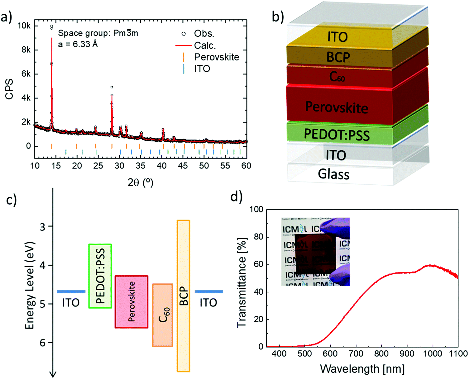 | ||
| Fig. 1 (a) XRD characterization of MA0.3FA0.7Pb0.5Sn0.5I3 perovskite thin films deposited on a glass/ITO substrate coated with PEDOT:PSS. Observed (experimental) intensities are marked with open circles, Le Bail fit is represented in red and Braggs’ reflection for the perovskite and underlying ITO phases are indicated with vertical markers of different colors. (b) Schematic device structure of the semi-transparent perovskite photodetector. (c) Schematic energy band diagram of the photodetector. (d) Transmittance of the same full stack with a 200 nm thick active layer. Inset: Photography of the device in front of the logo of the research institute where this work was carried out. | ||
Photodetectors using MA0.3FA0.7Pb0.5Sn0.5I3 perovskite thin films as active layer were fabricated (Fig. 1b). The devices had a p–i–n configuration with the following structure: glass/ITO/PEDOT:PSS (20 nm)/MA0.3FA0.7Pb0.5Sn0.5I3 (200 nm)/C60 (25 nm)/BCP (7 nm)/ITO (140 nm) (where PEDOT:PSS is poly(3,4-ethylenedioxythiophene) polystyrene sulfonate, C60 is fullerene and BCP is bathocuproine). The energy band diagram is shown in Fig. 1c. The energy levels of the perovskite layer are previously reported in literature.45 PEDOT:PSS and C60/BCP were chosen as hole and electron transport layers, respectively, as they have shown to be good candidates for these roles in Sn–Pb based solar cells.46 Usually, ITO top electrodes are processed by ion sputtering which can easily damage any soft organic underlayers,47 leading to increased leakage current, as well as reduced efficiency and lower lifetime of the device.47–49 To mitigate these limitations, pulsed laser deposition (PLD) is an alternative technique that allows damage-free smooth ITO deposition on top of thin organic layers. For example, in our recent investigation, bifacial MAPbI3 perovskite solar cells were fabricated by directly depositing ITO with PLD on top of the organic C60/BCP electron transport layers (ETLs) with a total thickness of only 32 nm, without any protective buffer layers in between, leading to no damage to the device stack underneath and, hence, no losses in photovoltaic performance.50 Therefore, for the fabrication of the semitransparent MA0.3FA0.7Pb0.5Sn0.5I3 photodetectors investigated here, the ITO top cathode was also deposited via PLD directly on top of the C60/BCP ETLs, using the optimized conditions previously obtained.50 In order to prove that the deposition of the ITO top electrode was not harmful to the organic stack underneath, reference devices with a standard opaque Cu top contact (100 nm), instead of ITO, were also prepared by thermal vacuum deposition, for comparison. Although the resistivity of the PLD-ITO films is quite low (between 0.4 to 1 mΩ cm, depending on the deposition pressure, for thicknesses of ca. 150 nm), it is not as low as a typical Cu film (usually around 1 μΩ cm). Therefore, to increase the conductivity of the ITO top cathode in the semitransparent devices, Au grids (100 nm thick) were thermally evaporated around the edges of the PLD-ITO cathode, but not covering the active area. This approach decreased the series resistance of devices finished with PLD-ITO from 17.4 to 4.8 mΩ cm−2, within the same order of magnitude as devices using the metal top contact (∼3.5 mΩ cm−2).50
The transmittance of the full stack using 200 nm perovskite films was measured (Fig. 1d). In the visible range, the devices are opaque from 380 to almost 600 nm and their transmission starts increasing in the red region, resulting in a characteristic dark red color (Fig. 1d, inset). More importantly, in the NIR the devices are semitransparent with a transmission of over 48% (780–1100 nm wavelength range). Of particular importance are the wavelengths of 850 and 940 nm as these are wavelengths where the most commonly available commercial NIR light-emitting diodes (LEDs) emit. The whole device showed transmittance of 54% and 56% at 850 and 940 nm, respectively.
Current density versus voltage (J–V) characteristics of the devices were obtained and are shown in Fig. 2a, both in dark (blue curve) and under light (green curve). The J–V sweep presents almost negligible hysteresis, usually originating from halide ionic migration on the active layer.51 The dark current density (JD) is 1.74 × 10⁻² mA cm−2 at −0.2 V. Light current density (JPh) was also measured by using a light source with a simulated AM 1.5G irradiation (100 mW cm−2). The JPh is 17.7 mA cm−2 at −0.2 V and we do not observe nearly any voltage dependence, highlighting the efficient charge carrier extraction of these devices. The JPh is three orders of magnitude higher than the JD (at −0.2 V). The EQE was measured at 0 V and under a constant voltage bias of −0.2, −0.4 and −0.6 V (Fig. 3b). There is virtually no voltage dependence of the EQE on the voltage, as expected form the current profile in the J–V curves under illumination. The devices absorb up to ca. 1050 nm, in line with the expected bandgap of the material (∼1.22 eV),41 with values of 23% and 13% for 850 and 940 nm, respectively. The EQE in the visible spectrum (380–780 nm) ranges from 30 to 77%. This shows that these photodetectors could be used for applications both in the visible and in the NIR range. On the other hand, for strict wavelength dependent applications, filters should be used to prevent parasitic light from reaching the active layer.20
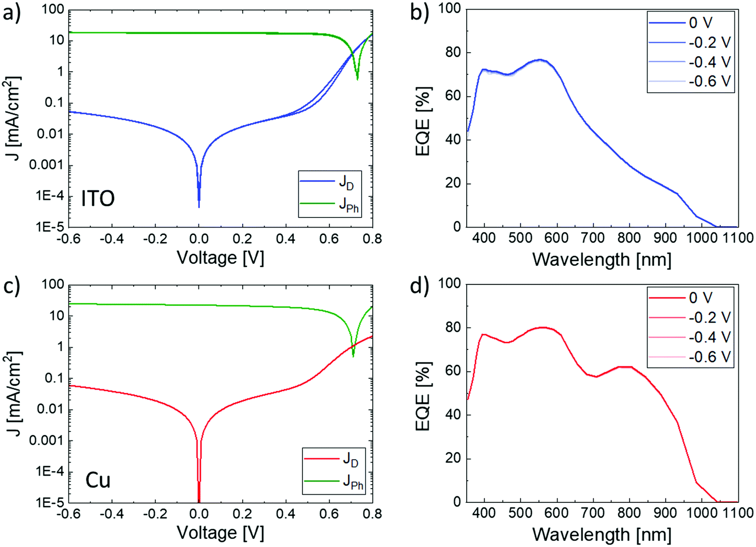 | ||
| Fig. 2 (a) J–V characteristics of the semitransparent Glass/ITO/PEDOT:PSS/MA0.3FA0.7Pb0.5Sn0.5I3/C60/BCP/ITO photodetector in dark (blue curve) and under light illumination (green curve). (b) EQE spectra for the same device measured at different voltage biases (0 to −0.6 V in 0.2 V steps). (c) J–V characteristics of the standard opaque Glass/ITO/PEDOT:PSS/MA0.3FA0.7Pb0.5Sn0.5I3/C60/BCP/Cu photodetector in dark (red curve) and under light (green curve). (d) EQE spectra for the same device measured at different voltage biases (0 to −0.6 V in 0.2 V steps). | ||
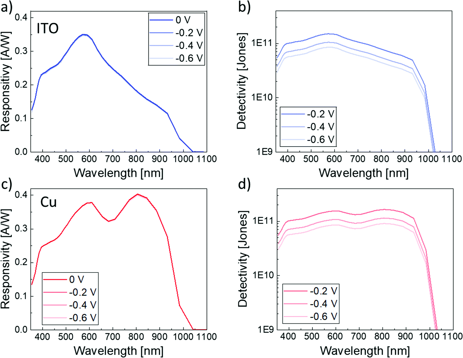 | ||
| Fig. 3 (a) Responsivity (R) as a function of wavelength of the semitransparent Glass/ITO/PEDOT:PSS/MA0.3FA0.7Pb0.5Sn0.5I3/C60/BCP/ITO photodetector at different voltage biases (0 to −0.6 V in 0.2 V steps). (b) Detectivity (D*) as a function of wavelength for the same device measured at different voltage biases (−0.2 V to −0.6 V in 0.2 V steps). (c) R as a function of wavelength of the standard opaque Glass/ITO/PEDOT:PSS/MA0.3FA0.7Pb0.5Sn0.5I3/C60/BCP/Cu photodetector at different voltage biases (0 to −0.6 V in 0.2 V steps). (d) D* as a function of wavelength for the same device measured at different voltage biases (−0.2 V to −0.6 V in 0.2 V steps). | ||
We compared the performance of these devices with reference devices using a standard opaque Cu top electrode (stack: glass/ITO/PEDOT:PSS/MA0.3FA0.7Pb0.5Sn0.5I3/C60/BCP/Cu). J–V curves of the reference devices are shown in Fig. 2c both in dark (red curve) and under the same light conditions (green curve). The JD and the JPh under −0.2 V are 1.92 × 10⁻² mA cm−2 and 23.4 mA cm−2, respectively. The JD for the semitransparent and reference devices exhibits very similar values, where small differences are attributed to device-to-device variation. The shape of both curves is also very similar between the PLD-ITO and the Cu top electrode devices, indicating that the PLD processing on top of the stack has not damaged the soft layers underneath; if the PLD had damaged the underlayers, the contact/shunt resistance of the semitransparent devices would have had increased,50 mainly affecting the slope of the J–V curves near short-circuit (from 0 to ∼0.7 V). The EQE, however, shows higher values for the reference device, all across the visible spectrum (58–80%), and at 850 nm (56%) and 940 nm (32%) (Fig. 3d). The higher EQE on the reference device is expected as the opaque electrode acts as a mirror, reflecting the non-absorbed light that crossed the device back to the active layer, where it can be reabsorbed.
The responsivity (R) is a key figure of merit that is defined as the ratio of the output photocurrent (IPh) and the input light power (PPh) at a certain wavelength and is expressed as:
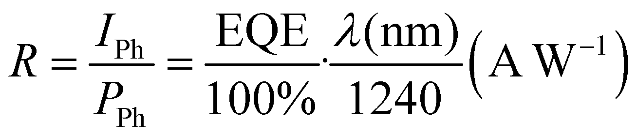 | (1) |
 | (2) |
The detectivity of the semitransparent devices at −0.2, −0.4 and −0.6 V was calculated (Fig. 3b). The D* is voltage dependent (as the JD varies with the applied voltage) and shows values of 6.6 × 10¹⁰ and 4.2 × 10¹⁰ Jones (at −0.2 V) for 850 and 940 nm, respectively. When comparing the detectivity of our devices with semitransparent devices based on commonly-used perovskite materials such as MAPbI3 or MAPbCl3 we observe that previous works report higher detectivity values (in the order of 1012 Jones, and up to 7.3 × 10¹² Jones),38,53 albeit these devices can absorb only in the UV and visible ranges, hindering their applicability in the NIR. An alternative to our approach would be to add a PbSe quantum dot layer on top of the MAPbI3 layer. In this way absorption can be enhanced up to 2600 nm, at the cost of a more complex device structure.40
Both R and D* were also determined for the reference opaque devices (Fig. 3c and d). In both cases, the values were higher (at −0.2 V) than the semitransparent devices with R of 0.39 and 0.24 A W−1 and D* of 1.6 × 10¹¹ and 9.2 × 10¹⁰ Jones (at −0.2 V) for 850 and 940 nm, respectively. Again, the higher values for the reference devices are related to the higher EQE exhibited by these devices due to the use of an opaque reflecting top contact. Therefore, it is difficult to directly compare the R and D* of the semitransparent device with other NIR perovskite photodetector works reported in the literature where an opaque reflective top contact is used.29 In order to improve the detectivity, JD has to be reduced, as EQE will always be limited by the thickness of the devices (due to the trade-off between EQE and transparency). Recently it has been shown that the origin of the dark current in perovskite photodetectors is due to the interfacial energy offset between the perovskite and the electron blocking layer (EBL).45 Carefully choosing an EBL with a lower highest occupied molecular orbital (HOMO) than PEDOT:PSS (e.g. poly(4-butyl-N,N-diphenylaniline) (poly-TPD)) could further improve the JD of these devices and will be subject of further study. Other strategies, such as using an edge cover layer, covering edges and corners of the pixels, have also been shown to be effective.43
Finally, the linearity of the semitransparent devices was examined at −0.6 V illuminating from both top and bottom sides. Fig. 4 shows the JPh as a function of the incident light intensity. In both cases the device behaves linearly in the 100 to 1 mW cm−2 light intensity range (R-square of 0.997 and 0.998 for top and bottom illumination, respectively), deviating at lower values due to the noise current of the device.54 These results indicate that the device has the same response irrespectively from the direction of the illumination and could effectively be used for applications where a high transparency (both in the visible and in the NIR) is needed, or as bifacial devices in a range of lighting conditions.
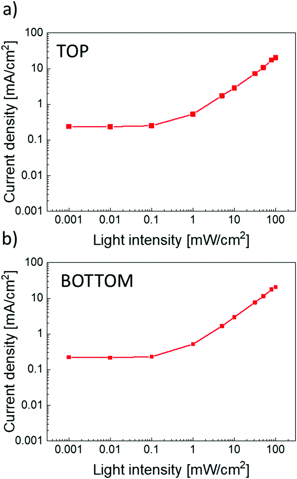 | ||
| Fig. 4 Linearity (current density vs. light power) of the semitransparent (ITO top contact) MA0.3FA0.7Pb0.5Sn0.5I3 perovskite photodetector illuminated from the (a) top and (b) bottom. | ||
Conclusions
We have reported a NIR semitransparent photodetector based on a MA0.3FA0.7Pb0.5Sn0.5I3 perovskite active layer with a full stack transmission of over 48% in the NIR (between 780 and 1100 nm). To achieve this, we have fabricated thin perovskite layers (200 nm) sandwiched between two semitransparent ITO electrodes. The top electrode was deposited via PLD, which is a soft deposition method harmless to the underlying organic stack. The photodetectors showed a dark current of 1.74 × 10⁻² mA cm−2 (at −0.2 V), EQEs of 23% and 13% and D* of 6.6 × 10¹⁰ and 4.2 × 10¹⁰ Jones (at −0.2 V) for 850 and 940 nm, respectively. No difference in the response was observed when illuminating from either side of the device at different light intensities. These findings could lead to the development of novel NIR semitransparent perovskite photodetectors that could open new application possibilities for this technology.Experimental section
Materials
PEDOT:PSS (Al 4083) was purchased from Heraeus Clevios. Dimethylformamide and dimethyl sulfoxide were purchased from VWR. Sn foil, anisole and SnF2 were purchased from Sigma Aldrich. Fullerene (C60) was purchased from Merck KGaA. CH3NH3I (MAI), CHNH2NH2I (FAI) and bathocuproine (BCP) were purchased from Luminescence Technology Corp. Tin iodide (SnI2) and lead iodide (PbI2) were purchased from Alfa Aesar.Device fabrication
ITO-coated glass substrates were subsequently cleaned with soap, water and isopropanol in an ultrasonic bath, followed by a 20 min UV-ozone treatment. PEDOT:PSS was filtered with a 0.45 μm polypropylene filter, then spin-coated on the ITO-coated glass substrates (4000 rpm for 30 seconds). Subsequently, the substrates were annealed at 150 °C for 10 minutes. For the preparation of the perovskite precursor molar ratios of 0.385 MAI, 0.165 FAI, 0.275 PbI2, 0.275 SnI2 and 0.0275 SnF2 (10% of SnI2 molar ratio) were mixed in DMF![[thin space (1/6-em)]](https://www.rsc.org/images/entities/char_2009.gif) :DMSO (3:1) with a resulting 0.55 M concentration. In order to suppress the Sn oxidation, a tin foil (1 cm2) was inserted in the precursor for 10 minutes. The precursor was filtered with a 0.45 μm polytetrafluoroethylene filter and spin-coated at 1000 rpm for 10 seconds and 4000 rpm for 40 seconds. The anisole was dropped dynamically on the substrate. Sequentially, the samples were annealed at 100 °C for 10 minutes. Finally, 140 nm of ITO were deposited by PLD using a Solmates’ large area PLD 200 mm system coupled to a Lightmachinery's IPEX-700 KrF excimer laser (λ = 248 nm, with a repetition rate of 25 Hz and a fluence of 1.5–1.7 J cm−2). The source material for ITO deposition was a Sn:In2O3 ceramic target with 2:98 wt% and the chamber pressure was set at 0.033 mbar, with an O2 partial pressure of 0.007 mbar controlled by a constant injection of an oxygen/argon gas mix, as optimized in our previous paper.50 Shadow masks were used during the ITO deposition to obtain a final active area of 0.06 cm2. The Au grids (100 nm thick) at the side of the PLT-ITO cathodes were thermally evaporated. The devices were prepared in an inert atmosphere inside the glovebox and characterized outside. Prior to the characterization, the stacks were encapsulated using atomic layer deposition for the deposition of a transparent Al2O3 (30 nm) film at 40 °C to prevent possible degradation from ambient conditions.55
:DMSO (3:1) with a resulting 0.55 M concentration. In order to suppress the Sn oxidation, a tin foil (1 cm2) was inserted in the precursor for 10 minutes. The precursor was filtered with a 0.45 μm polytetrafluoroethylene filter and spin-coated at 1000 rpm for 10 seconds and 4000 rpm for 40 seconds. The anisole was dropped dynamically on the substrate. Sequentially, the samples were annealed at 100 °C for 10 minutes. Finally, 140 nm of ITO were deposited by PLD using a Solmates’ large area PLD 200 mm system coupled to a Lightmachinery's IPEX-700 KrF excimer laser (λ = 248 nm, with a repetition rate of 25 Hz and a fluence of 1.5–1.7 J cm−2). The source material for ITO deposition was a Sn:In2O3 ceramic target with 2:98 wt% and the chamber pressure was set at 0.033 mbar, with an O2 partial pressure of 0.007 mbar controlled by a constant injection of an oxygen/argon gas mix, as optimized in our previous paper.50 Shadow masks were used during the ITO deposition to obtain a final active area of 0.06 cm2. The Au grids (100 nm thick) at the side of the PLT-ITO cathodes were thermally evaporated. The devices were prepared in an inert atmosphere inside the glovebox and characterized outside. Prior to the characterization, the stacks were encapsulated using atomic layer deposition for the deposition of a transparent Al2O3 (30 nm) film at 40 °C to prevent possible degradation from ambient conditions.55
X-ray diffraction
The patterns were collected in Bragg–Brentano geometry on an Empyrean PANalytical powder diffractometer with a copper anode operated at 45 kV and 40 mA. Further analysis including Le Bail fits were performed with Fullprof software.Optical and optoelectronic characterization
The transmittance was measured with an Avantes AvaLight-DS-S-BAL deuterium halogen light source and an Avantes AvaSpec-2048L spectrometer. The J–V curves of the devices were measured with a Keithley 2612A SourceMeter under dark and illuminated with a Wavelabs Sinus 70 LED solar simulator (AM 1.5G irradiation (100 mW cm−2)) and recorded using a custom LabVIEW program. A step of 0.01 voltage was used. The light intensity was calibrated before every measurement using a calibrated Si reference diode. Intensity dependent data was carried out by measuring J–V curves in the same system using neutral density filters of decreasing optical density. The external quantum efficiency (EQE) was measured using a Quartz-Tungsten-Halogen lamp (Newport Apex 2-QTH) source, a monochromator (Newport CS130-USB-3-MC), a chopper (at 279 Hz) and a focusing lens. The device current was measured as a function of energy using a lock-in amplifier (Stanford Research Systems SR830) and recorded using a custom LabVIEW program. The system was calibrated, and the solar spectrum mismatch was corrected using a calibrated Si reference cell.Conflicts of interest
The authors have no conflict of interest to declare.Acknowledgements
We acknowledge support from the Comunitat Valenciana (PROMETEU/2020/077, APOSTD/2021/368), the Spanish Ministry of Science and Innovation (MCIN) and the Spanish State Research Agency (AEI): projects MAT2017-88821-R and RTI2018-095362-A-I00 funded by MCIN/AEI/10.13039/501100011033 and by ‘‘ERDF A way of making Europe’’; project PCI2020-112084 funded by MCIN/AEI/10.13039/501100011033 and by the ‘‘European Union NextGenerationEU/PRTR’’; grant RYC-2016-21316 and PRE2018-084619 funded by MCIN/AEI/10.13039/501100011033 and by ‘‘ESF Investing in your future’’.References
- A. Rogalski, J. Antoszewski and L. Faraone, J. Appl. Phys., 2009, 105, 91101 CrossRef.
- E. K. Bolton, G. S. Sayler, D. E. Nivens, J. M. Rochelle, S. Ripp and M. L. Simpson, Sens. Actuators, BSens. Actuators, B, 2002, 85, 179–185 CrossRef CAS.
- S. Kim, Y. T. Lim, E. G. Soltesz, A. M. De Grand, J. Lee, A. Nakayama, J. A. Parker, T. Mihaljevic, R. G. Laurence, D. M. Dor, L. H. Cohn, M. G. Bawendi and J. V. Frangioni, Nat. Biotechnol., 2004, 22, 93–97 CrossRef CAS PubMed.
- D. Tordera, B. Peeters, H. B. Akkerman, A. J.-J. M. van Breemen, J. Maas, S. Shanmugam, A. J. Kronemeijer and G. H. Gelinck, Adv. Mater. Technol., 2019, 4, 1900651 CrossRef CAS.
- T. Yokota, T. Nakamura, H. Kato, M. Mochizuki, M. Tada, M. Uchida, S. Lee, M. Koizumi, W. Yukita, A. Takimoto and T. Someya, Nat. Electron., 2020, 3, 113–121 CrossRef.
- T. Yokota, P. Zalar, M. Kaltenbrunner, H. Jinno, N. Matsuhisa, H. Kitanosako, Y. Tachibana, W. Yukita, M. Koizumi and T. Someya, Sci. Adv., 2016, 2, e1501856 CrossRef PubMed.
- D. C. Ng, T. Tokuda, A. Yamamoto, M. Matsuo, M. Nunoshita, H. Tamura, Y. Ishikawa, S. Shiosaka and J. Ohta, Sens. Actuators, B, 2006, 119, 262–274 CrossRef CAS.
- C.-H. Chen, C.-F. Lin, K.-H. Wang, H.-C. Liu, H.-W. Zan, H.-F. Meng, W. Hortschitz, H. Steiner, A. Kainz and T. Sauter, Org. Electron., 2017, 49, 305–312 CrossRef CAS.
- C. Harbeck, R. Faurie and T. Scheper, Anal. Chim. Acta, 2004, 501, 249–253 CrossRef CAS.
- L. Rey-Barroso, F. J. Burgos-Fernández, X. Delpueyo, M. Ares, S. Royo, J. Malvehy, S. Puig and M. Vilaseca, Sensors, 2018, 18, 1441 CrossRef PubMed.
- H. Akkerman, B. Peeters, A. van Breemen, S. Shanmugam, L. Ugalde Lopez, D. Tordera, R. van de Ketterij, E. Delvitto, R. Verbeek, P. Malinowski, T.-H. Ke, F. De Roose, L. Moreno Hagelsieb, I. Katsouras, A. J. Kronemeijer, E. Meulenkamp and G. Gelinck, J. Soc. Inf. Disp., 2021, 29, 935–947 CrossRef.
- P. E. Malinowski, A. Nakamura, D. Janssen, Y. Kamochi, I. Koyama, Y. Iwai, A. Stefaniuk, E. Wilenska, C. Salas Redondo, D. Cheyns, S. Steudel and P. Heremans, Org. Electron., 2014, 15, 2355–2359 CrossRef CAS.
- A. Colsmann, A. Puetz, A. Bauer, J. Hanisch, E. Ahlswede and U. Lemmer, Adv. Energy Mater., 2011, 1, 599–603 CrossRef CAS.
- Y. Xie, R. Xia, T. Li, L. Ye, X. Zhan, H. L. Yip and Y. Sun, Small Methods, 2019, 3, 1900424 CrossRef CAS.
- V. V. Brus, J. Lee, B. R. Luginbuhl, S. J. Ko, G. C. Bazan and T. Q. Nguyen, Adv. Mater., 2019, 31, 1900904 CrossRef PubMed.
- H. Schmidt, H. Flügge, T. Winkler, T. Bülow, T. Riedl and W. Kowalsky, Appl. Phys. Lett., 2009, 94, 243302 CrossRef.
- D. Tordera, A. J.-J. M. van Breemen, A. J. Kronemeijer, J.-L. van der Steen, B. Peeters, S. Shanmugan, H. B. Akkerman and G. H. Gelinck, Organic Flexible Electronics, Elsevier, 2021, pp. 575–597 Search PubMed.
- J. Kim, S.-M. Kwon, Y. K. Kang, Y.-H. Kim, M.-J. Lee, K. Han, A. Facchetti, M.-G. Kim and S. K. Park, Sci. Adv., 2019, 5, eaax8801 CrossRef CAS PubMed.
- S. Tong, H. Wu, C. Zhang, S. Li, C. Wang, J. Shen, S. Xiao, J. He, J. Yang, J. Sun and Y. Gao, Org. Electron., 2017, 49, 347–354 CrossRef CAS.
- D. Tordera, B. Peeters, E. Delvitto, S. Shanmugam, J. Maas, J. de Riet, R. Verbeek, R. van de Laar, T. Bel, G. Haas, L. Ugalde, A. van Breemen, I. Katsouras, A. J. Kronemeijer, H. Akkerman, E. Meulenkamp and G. Gelinck, J. Soc. Inf. Disp., 2020, 28, 381–391 CrossRef CAS.
- V. M. Goldschmidt, Naturwissenschaften, 1926, 14, 477–485 CrossRef CAS.
- A. Kojima, K. Teshima, Y. Shirai and T. Miyasaka, J. Am. Chem. Soc., 2009, 131, 6050–6051 CrossRef CAS PubMed.
- X. Peng, J. Yuan, S. Shen, M. Gao, A. S.-R. Chesman, H. Yin, J. Cheng, Q. Zhang and D. Angmo, Adv. Funct. Mater., 2017, 27, 1703704 CrossRef.
- L. Gil-Escrig, C. Momblona, M. G. La-Placa, P. P. Boix, M. Sessolo and H. J. Bolink, Adv. Energy Mater., 2018, 8, 1703506 CrossRef.
- N. J. Jeon, J. H. Noh, W. S. Yang, Y. C. Kim, S. Ryu, J. Seo and S. Il Seok, Nature, 2015, 517, 476–480 CrossRef CAS PubMed.
- J. Jeong, M. Kim, J. Seo, H. Lu, P. Ahlawat, A. Mishra, Y. Yang, M. A. Hope, F. T. Eickemeyer, M. Kim, Y. J. Yoon, I. W. Choi, B. P. Darwich, S. J. Choi, Y. Jo, J. H. Lee, B. Walker, S. M. Zakeeruddin, L. Emsley, U. Rothlisberger, A. Hagfeldt, D. S. Kim, M. Grätzel and J. Y. Kim, Nature, 2021, 592, 381–385 CrossRef CAS PubMed.
- Y. Wang, D. Yang, X. Zhou, S. M. Alshehri, T. Ahamad, A. Vadim and D. Ma, Org. Electron., 2017, 42, 203–208 CrossRef CAS.
- T. Hellmann, C. Das, T. Abzieher, J. A. Schwenzer, M. Wussler, R. Dachauer, U. W. Paetzold, W. Jaegermann and T. Mayer, Adv. Energy Mater., 2020, 10, 2002129 CrossRef CAS.
- J. Miao and F. Zhang, J. Mater. Chem. C, 2019, 7, 1741–1791 RSC.
- F. P. de Arquer, X. Gong, R. P. Sabatini, M. Liu, G.-H. Kim, B. R. Sutherland, O. Voznyy, J. Xu, Y. Pang, S. Hoogland, D. Sinton and E. Sargent, Nat. Commun., 2017, 8, 14757 CrossRef PubMed.
- C. Liu, K. Wang, P. Du, E. Wang, X. Gong and A. J. Heeger, Nanoscale, 2015, 7, 16460–16469 RSC.
- A. Waleed, M. M. Tavakoli, L. Gu, Z. Wang, D. Zhang, A. Manikandan, Q. Zhang, R. Zhang, Y.-L. Chueh and Z. Fan, Nano Lett., 2017, 17, 523–530 CrossRef CAS PubMed.
- Y. Zhao, C. Li, J. Jiang, B. Wang and L. Shen, Small, 2020, 16, 2001534 CrossRef CAS PubMed.
- H. L. Zhu, H. Lin, Z. Song, Z. Wang, F. Ye, H. Zhang, W. J. Yin, Y. Yan and W. C.-H. Choy, ACS Nano, 2019, 13, 11800–11808 CrossRef CAS PubMed.
- Y. Ogomi, A. Morita, S. Tsukamoto, T. Saitho, N. Fujikawa, Q. Shen, T. Toyoda, K. Yoshino, S. S. Pandey, T. Ma and S. Hayase, J. Phys. Chem. Lett., 2014, 5, 1004–1011 CrossRef CAS PubMed.
- F. Hao, C. C. Stoumpos, R. P.-H. Chang and M. G. Kanatzidis, J. Am. Chem. Soc., 2014, 136, 8094–8099 CrossRef CAS PubMed.
- Y. Wang, C. Chen, T. Zou, L. Yan, C. Liu, X. Du, S. Zhang and H. Zhou, Adv. Mater. Technol., 2020, 5, 1900752 CrossRef CAS.
- F. Cao, W. Tian, M. Wang, H. Cao and L. Li, Adv. Funct. Mater., 2019, 29, 1901280 CrossRef.
- R. Xu, L. Min, Z. Qi, X. Zhang, J. Jian, Y. Ji, F. Qian, J. Fan, C. Kan, H. Wang, W. Tian, L. Li, W. Li and H. Yang, ACS Appl. Mater. Interfaces, 2020, 12, 16462–16468 CrossRef CAS PubMed.
- T. Zhu, Y. Yang, L. Zheng, L. Liu, M. L. Becker and X. Gong, Adv. Funct. Mater., 2020, 30, 1909487 CrossRef CAS.
- R. Lin, K. Xiao, Z. Qin, Q. Han, C. Zhang, M. Wei, M. I. Saidaminov, Y. Gao, J. Xu, M. Xiao, A. Li, J. Zhu, E. H. Sargent and H. Tan, Nat. Energy, 2019, 4, 864–873 CrossRef CAS.
- K. Xiao, R. Lin, Q. Han, Y. Hou, Z. Qin, H. T. Nguyen, J. Wen, M. Wei, V. Yeddu, M. I. Saidaminov, Y. Gao, X. Luo, Y. Wang, H. Gao, C. Zhang, J. Xu, J. Zhu, E. H. Sargent and H. Tan, Nat. Energy, 2020, 5, 870–880 CrossRef CAS.
- A. J.-J. M. van Breemen, R. Ollearo, S. Shanmugam, B. Peeters, L. C.-J. M. Peters, R. L. van de Ketterij, I. Katsouras, H. B. Akkerman, C. H. Frijters, F. Di Giacomo, S. Veenstra, R. Andriessen, R. A.-J. Janssen, E. A. Meulenkamp and G. H. Gelinck, Nat. Electron., 2021, 4, 818–826 CrossRef CAS.
- W. Wang, D. Zhao, F. Zhang, L. Li, M. Du, C. Wang, Y. Yu, Q. Huang, M. Zhang, L. Li, J. Miao, Z. Lou, G. Shen, Y. Fang and Y. Yan, Adv. Funct. Mater., 2017, 27, 1703953 CrossRef.
- R. Ollearo, J. Wang, M. J. Dyson, C. H.-L. Weijtens, M. Fattori, B. T. van Gorkom, A. J.-J. M. van Breemen, S. C.-J. Meskers, R. A.-J. Janssen and G. H. Gelinck, Nat. Commun., 2021, 12, 7277 CrossRef CAS PubMed.
- D. Zhao, Y. Yu, C. Wang, W. Liao, N. Shrestha, C. R. Grice, A. J. Cimaroli, L. Guan, R. J. Ellingson, K. Zhu, X. Zhao, R. G. Xiong and Y. Yan, Nat. Energy, 2017, 2, 17018 CrossRef CAS.
- E. Aydin, C. Altinkaya, Y. Smirnov, M. A. Yaqin, K. P.-S. Zanoni, A. Paliwal, Y. Firdaus, T. G. Allen, T. D. Anthopoulos, H. J. Bolink, M. Morales-Masis and S. De Wolf, Matter, 2021, 4, 3549–3584 CrossRef CAS.
- H. Kanda, A. Uzum, A. K. Baranwal, T. A.-N. Peiris, T. Umeyama, H. Imahori, H. Segawa, T. Miyasaka and S. Ito, J. Phys. Chem. C, 2016, 120, 28441–28447 CrossRef CAS.
- Q. H. Fan, M. Deng, X. Liao and X. Deng, J. Appl. Phys., 2009, 105, 33304 CrossRef.
- K. P.-S. Zanoni, A. Paliwal, M. A. Hernández-Fenollosa, P.-A. Repecaud, M. Morales-Masis and H. J. Bolink, Adv. Mater. Technol., 2022, 2101747 CrossRef.
- D.-H. Kang and N.-G. Park, Adv. Mater., 2019, 31, 1805214 CrossRef PubMed.
- Y. Fang, A. Armin, P. Meredith and J. Huang, Nat. Photonics, 2019, 13, 1–4 CrossRef CAS.
- V. Adinolfi, O. Ouellette, M. I. Saidaminov, G. Walters, A. L. Abdelhady, O. M. Bakr and E. H. Sargent, Adv. Mater., 2016, 28, 7264–7268 CrossRef CAS PubMed.
- R. D. Jansen-van Vuuren, A. Armin, A. K. Pandey, P. L. Burn and P. Meredith, Adv. Mater., 2016, 28, 4766–4802 CrossRef CAS PubMed.
- I. C. Kaya, K. P.-S. Zanoni, F. Palazon, M. Sessolo, H. Akyildiz, S. Sonmezoglu and H. J. Bolink, Adv. Energy Sustainable Res., 2021, 2, 2000065 CrossRef.
Footnote |
| † Authors contributed equally to this work. |
| This journal is © The Royal Society of Chemistry 2022 |