
 Open Access Article
 This Open Access Article is licensed under a Creative Commons Attribution-Non Commercial 3.0 Unported Licence
Getting closer to the intrinsic properties of Ni2+salen polymer semiconductors accessed by chain isolation inside silica nanochannels†
Kamila
Łępicka
 *a,
Piyush Sindhu
Sharma
a,
Paweł
Borowicz
a,
Grégory
Francius
b and
Alain
Walcarius
*b
*a,
Piyush Sindhu
Sharma
a,
Paweł
Borowicz
a,
Grégory
Francius
b and
Alain
Walcarius
*b
aInstitute of Physical Chemistry, Polish Academy of Sciences, Kasprzaka 44/52, 01-224 Warsaw, Poland. E-mail: klepicka@ichf.edu.pl
bLaboratoire de Chimie Physique et Microbiologie Pour les Matériaux et l’Environnement, LCPME, UMR 7564 CNRS – Université de Lorraine, 405 rue de Vandoeuvre, Villers-lès-Nancy, F-54600, France. E-mail: alain.walcarius@univ-lorraine.fr
First published on 9th May 2022
Abstract
The scientific problem aimed to be solved by our research is to improve the charge transport of Ni2+salen polymer semiconductors by isolation of individual chains inside mesoporous silica channels capable of ensuring the suppression of interchain interactions that cause the charge carrier trapping in the continuous polymer films. Elimination of charge trapping is the primary motivation for energy transport improvement in polymer semiconductors serving as interconnections in molecular electronics. With this in mind, we prepared molecular wires based on structurally privileged ortho substituted Ni2+salens, offering the molecular structure facilitating its linear electropolymerization growth inside the confined space of a silica matrix containing vertical channels that are 2 nm in diameter. We noticed that the analogical embedment of ortho unsubstituted poly(Ni2+salen)s was not possible. Thus, we used quantum chemical calculations utilizing density functional theory to explain this phenomenon. Hence, we succeeded in recognizing structure–property relationships of Ni2+salens governing their local electropolymerization ability inside vertical nanochannels. Isolation of polymer chains allowed us to gain insight into the intrinsic properties of Ni2+salen polymers creating a better understanding of their charge transport and polymerization mechanisms. The prepared molecular wires exhibited improved electronic properties evidenced by electrochemical measurements revealing the energetically favored charge transporting polymer forms and the increased ratio between anodic and cathodic charges. Furthermore, we directly evidenced the presence of a Ni2+salen polymer inside silica nanochannels using high-resolution X-ray photoelectron spectroscopy combined with very low-energy argon ion beam sputtering, as well as using atomic force microscopy and transmission electron microscopy.
1. Introduction
One of the ongoing interests in fabricating semiconductor polymer based materials is focused on one-dimensional (1D) nanostructures and their optimization for application in molecular-scale devices ranging from size selective catalysts and chemical sensors to nanoscale electronics.1 A considerable amount of work was directed towards the preparation of vertical polymer structures using hard and soft templates and to investigate the dependence of their properties on dimensionality and size reduction.2 However, their diameters were typically limited to tens of nanometers, thus indicating that individual nanowires were made of several polymeric chains. Utilization of the nanoengineering tools delivered from all branches of materials science allowed a further step by fabricating conducting polymer systems with isolated chains harvesting the energy to the directed locations.3–5 Thus, obtaining information about the way of improvement and optimization of a new polymer based system, for example, via encapsulation in non-conducting mesoporous silica frameworks,3,6 may lead to efficient charge transport while avoiding the charge carriers localization (charge carrier traps) usually observed in the bulk continuous polymer films.7 In particular, when using for this purpose electrochemical polymerization, both molecular transport of monomers within mesoporous silica channels8 and charge transport control in insulating media9 have to be considered.During template-free polymerization of monomers containing in their structure aromatic systems or simple unsaturated bonds, the growing polymer semiconductor counterparts tend to interact, e.g., by π–π stacking or in another weak intermolecular manner, thus causing uncontrolled chain growth in all favored directions and conformational disorders.7,10 This way of polymer formation had a negative effect on the polymer conduction pathway.11 In such bulk polymer semiconductors, charge transport can be limited by interchain energy flow through space between different chains, or in some cases within one polymer segment, i.e., hopping of charge carriers between the polymer parts that are physically located within a Förster transfer radius, shortening conjugation lengths.12 The solution for this problem can be the separation of polymer chains to obtain control of the energy transfer through the ‘space within one polymer segment’ by their encapsulation in the cylindrical mesopores of a dielectric material, e.g., silica.12,13 Moreover, it was assumed that polymer incorporation into mesoporous channels forces the polymer chains to become straighter, increasing the conjugation length.12
The geometry of the silica hard template with vertical nanochannels separated by a few nm offers the possibility of controlling the orientation of polymer architectures and, thus, the control over energy transport in isolated polymer deposits. In parallel, a convenient method utilizing electrochemistry for preparing highly ordered and defect-free mesoporous silica templates with nanochannels oriented perpendicularly to the underlying electrode named electrochemically assisted self-assembly (EASA) was developed.14 Notably, the mesoporous silica matrix of vertical channels prepared by EASA retains the organization and orientation over a wide area, even after template removal, without cracks larger than the mesopore size.15 This hard template approach provided the possibility of the electrode material architecture control through its periodically and uniformly distributed hexagonal pattern of open forms with fixed diameters (i.e., mesopores, 2–3 nm in diameter), closed to species larger than the pore apertures but available for properly chosen molecules that were non-size-excluded.16
Electrodeposited Prussian blue within vertically aligned silica nanochannels initiated the direction of research oriented towards the preparation of the oriented objects in mesoporous silica films prepared by EASA and pointed out the need to develop an appropriate methodology based on the use of redox probes to optimize their access to the interior of the pores.17 Then, the approach was supplemented with the preparation of silica nanocomposites with well-known polyaniline (PANI), indicating improved electrochemical properties compared to those of bulky polymer deposits.6,18,19
However, the local deposition of conducting polymers inside such small mesopores is still a big challenge. The diameter of the ‘templating open form’ limits the size of the monomer used for the preparation of nanocomposites with a polymer encapsulated inside.6,20 Furthermore, not only the size of the monomer is crucial for polymer growth inside the template but also geometric compatibility with the hard template arrangement is a prerequisite. Moreover, the directions of polymer growth are dependent on the intrinsic properties of charge distribution in monomers and properly tuned polymerization conditions.
The number of polymer defects defined as a tendency of its aggregation is found to be solvent- and monomer concentration-dependent. It can be tuned by changing the chemical nature of the solvent and the concentration of the polymer precursor.21 Some reports claimed deposition of structures larger than 2–3 nm in diameter ‘inside’ the mesoporous template. For instance, 6 nm in diameter wires of polythiophene22 or palladium nanorods23 that were 50 nm in diameter were probably deposited outside the mesoporous template. Hence, a methodology to evidence a molecular level deposition of the material inside the mesopores is needed.
Notably, only the material embedded inside the mesoporous silica gives a chance for energy transport with a minimum loss, thus implicating material improvement and the possibility of its application in molecular-scale devices, where accumulated and released energy can be directed to desired locations.3 Because of this, understanding polymer electroactivity changes evoked by its confinement in the mesoporous matrix is critical for the successful fabrication of highly efficient and stable functional materials for molecular scale electronics and sensing.
Among conducting polymers, based on monomers with a size smaller than the mesopore diameter, PANI,6,18,24 PPy,5 and less known Ni2+salen based polymers are electroactive in the positive potential range, thus revealing p-type doping.25 The latter form multi-redox systems in which Ni2+ ions are linked through redox-active π-conjugated ligand sites.26 The Ni2+salen polymer behaves like a polyphenylene, with the Ni2+ ions acting as a bridge between biphenylene moieties.27 The group of Ni2+salen based polymers is assigned to polymeric semiconductors that reveal a mixed redox and π-conjugated conductivity. Their faradaic charge conduction mechanism can be explained in a simplified way as the transport of delocalized valence electrons28 using the model of Peierls distorted polymer lattice,29 such as that for polyphenylene type polymers. Importantly, this charge transport occurs only in a particular continuous range of potentials involving oxidized polymer forms, where no metal-centered oxidation, such as Ni2+/Ni3+, is observed.27,30,31 Electro-generated continuous films of Ni2+salen polymers of different chemical structures were applied as electrochromic devices,32 supercapacitor electrode materials,33 or precursors of heterogeneous catalysts.34 However, the mechanistic details considering the structure–reactivity requirements governing their charge transport and polymerization mechanism are still debated. Some reports explained the polymerization and charge propagation mechanism of Ni2+salen type polymers based on non-covalent stacking.35–38 This mechanism is described as an assembly of stacks during anodic polymerization, which forms at the expense of a donor–acceptor interaction between the ligand part of one monomer fragment and the metallic center of the other. The charge transport mechanism is described as an electron exchange between neighboring nickel centers. Some recent studies have described electropolymerization of Ni2+salen type complexes with a similar mechanism.39–41 To the best of our knowledge, there are no reports about the deposition of Ni2+salen polymers inside confined nanometer-scale space. Furthermore, there are no reports considering Ni2+salen molecular structure demands leading to such molecular level deposition process.
In the present work, we describe the preparation of polymeric Ni2+salen molecular wires isolated from each other. The molecular wires of an ortho substituted Ni2+salen polymer named poly(meso-NisaldMe-3dMe) were confined in a well-ordered, hexagonally packed, and vertically aligned silica nanochannel (2 nm in diameter) matrix by potentiodynamic electropolymerization. We employed electrochemical techniques to probe the charge transport performance of isolated poly(meso-NisaldMe-3dMe) molecular wires and compared them to those of a continuous poly(meso-NisaldMe-3dMe) film. Moreover, we applied a holistic physicochemical methodology to evidence a molecular level deposition of the material inside the silica nanochannels. Our approach revealed the necessity of using high-resolution X-ray photoelectron spectroscopy (XPS) combined with very low-energy argon ion beam sputtering for the direct evidence of polymer wires inside silica channels combined with nanomaterial component visualization by atomic force microscopy (AFM) and transmission electron microscopy (TEM). Moreover, as supported by computational modeling, we point out the required structural features of Ni2+salen monomers that enabled their local electropolymerization inside the confined space of mesoporous channels. The three Ni2+salen complexes investigated in this work are depicted in Scheme 1: meso-NiSaldMe-3dMe (1), meso-NiSaldMe (2), and NiSaltMe (3).
 | ||
| Scheme 1 Structural formulas of (1) meso-NiSaldMe-3dMe, (2) meso-NiSaldMe, and (3) NiSaltMe monomers. | ||
2. Experimental section
2.1. Chemicals
Cetyltrimethylammonium bromide, (CTAB, ≥99%, pure) was purchased from Acros Organics, tetraethoxysilane (TEOS, 98%, pure) was obtained from Alfa Aesar, and sodium nitrate (NaNO3, 99%, pure) was purchased from Fluka.Tetra(n-butyl)ammonium hexafluorophosphate, [(TBA)PF6, puriss, electrochemical grade], propylene carbonate (anhydrous, electrochemical grade), 1 N hydrochloric acid (HCl), ethanol (EtOH, HPLC grade), acetone (HPLC grade) and bis(pentamethylcyclopentadienyl)iron, (decamethylferrocene) ≥97%, pure were purchased from Sigma-Aldrich and used without further purification.
The monomeric Ni2+ salen based complexes, viz., meso-NiSaldMe-3dMe, meso-NiSaldMe, and NiSaltMe, were synthesized according to procedures described earlier.42,43
2.2 Mesoporous silica matrix formation
CTAB-templated mesoporous silica films were deposited on indium tin oxide (ITO) (surface resistivity 8–12 Ω, Delta Technologies) electrode surfaces by EASA.14 The perpendicular growth of silica around self-assembled CTAB micelles was initiated electrochemically under potentiostatic conditions by applying a potential of −1.3 V vs. a Ag/Ag+ pseudo-reference electrode for 20 s to the ITO electrode immersed in a 2.5 h hydrolyzed sol solution. The sol solution contained 100 mM TEOS as the silica precursor, 32 mM CTAB as the surfactant, and 0.1 M NaNO3 dissolved in a mixture of water and ethanol (1![[thin space (1/6-em)]](https://www.rsc.org/images/entities/char_2009.gif) :1, v/v). Before hydrolysis, the pH of the sol solution was adjusted to 3 by the addition of 0.1 M HCl. Application of a constant negative potential resulted in a local pH change at the electrode|solution interface caused by the electrochemical reduction of water. Consequently, this reaction produces hydroxide anions (OH−) likely to catalyze the polycondensation of TEOS around preformed CTAB hemimicelles and mesoporous silica film growth vertically to the ITO surface. The polycondensation of the silica precursor was quenched immediately by rinsing the electrode with an abundant amount of distilled water after removing the electrode from the sol solution. The silica coated electrodes were consolidated by keeping them overnight at 130 °C. This facilitated crosslinking of silica walls. In order to remove CTAB from the mesochannels of resulting silica coatings, prepared electrodes were kept for 20 minutes in the ethanol solution containing 0.1 M HCl. Next, these electrodes were rinsed with distilled water, ethanol, and acetone, respectively. Additionally, to remove water traces, extracted electrodes were dried overnight in an oven at 130 °C.
:1, v/v). Before hydrolysis, the pH of the sol solution was adjusted to 3 by the addition of 0.1 M HCl. Application of a constant negative potential resulted in a local pH change at the electrode|solution interface caused by the electrochemical reduction of water. Consequently, this reaction produces hydroxide anions (OH−) likely to catalyze the polycondensation of TEOS around preformed CTAB hemimicelles and mesoporous silica film growth vertically to the ITO surface. The polycondensation of the silica precursor was quenched immediately by rinsing the electrode with an abundant amount of distilled water after removing the electrode from the sol solution. The silica coated electrodes were consolidated by keeping them overnight at 130 °C. This facilitated crosslinking of silica walls. In order to remove CTAB from the mesochannels of resulting silica coatings, prepared electrodes were kept for 20 minutes in the ethanol solution containing 0.1 M HCl. Next, these electrodes were rinsed with distilled water, ethanol, and acetone, respectively. Additionally, to remove water traces, extracted electrodes were dried overnight in an oven at 130 °C.
2.3. Electrochemical cell configuration and electrodeposition conditions
Poly(meso-NiSaldMe-3dMe) based molecular wires and continuous film were prepared in a three-electrode cell configuration by electropolymerization under potentiodynamic conditions from the propylene carbonate solution containing 0.5 mM monomer and 0.1 M (TBA)PF6 in the potential range of 0.0 to 1.7 V vs. Ag/Ag+ at 100 mV s−1. The propylene carbonate solution of 0.1 M (TBA)PF6 was selected as an electropolymerization medium as it enables formation of Ni2+salen polymers with high operational stability upon doping and dedoping cycling,42,44,45 contrary to, e.g. (TBA)ClO4 in acetonitrile, for which entrapment of perchlorate anions may lead to poorer long-term stability.32,43 Two types of working electrodes were used, a bare ITO substrate and an ITO electrode coated with a mesoporous silica matrix, both with a geometrical area of 0.78 cm2 and comparable electrochemically active areas (curves 1 and 3 in Fig. S1, ESI†). The platinum mesh and silver wire were used as the counter and pseudo reference electrodes, respectively. The polymerization progress was controlled by the charge integration function implemented in EC-Lab software version 11.31 from BioLogic. Both electrodepositions were accomplished by passing ∼30 mC through a polymerization cell. The polymerization charges constituted the sum of the integrals under subsequent current–time polymerization curves. After electrodeposition, electrodes were rinsed with abundant propylene carbonate solvent before further use. The electrochemical responses were recorded, in a three-electrode system, in a monomer-free solution of 0.1 M (TBA)PF6 in propylene carbonate.2.4 Apparatus
All electrochemical experiments, including mesoporous silica deposition under potentiostatic conditions, polymer growth under potentiodynamic conditions, as well as the cyclic voltammetry (CV) and electrochemical impedance spectroscopy (EIS) measurements, were performed using a VSP electrochemistry system from BioLogic (SP 150) Science Instruments controlled by EC-Lab software from the same manufacturer. Before the EIS measurements, mesoporous silica and poly(meso-NiSaldme-3dMe) wire composite electrodes were equilibrated by applying a selected potential for 30 s. After this time, the current reached equilibrium, and then EIS measurements were performed at a voltage amplitude of 10 mV in the frequency range of 100 kHz to 10 mHz.AFM imaging was carried out in the PeakForce Quantitative Nanomechanical Mapping (QNM) mode, in air, using a Bioscope Resolve (Bruker Nano Surface, Bruker France SAS, Palaiseau, France). Silicon nitride cantilevers of a conical shape and with a spring constant of ∼0.35 nN nm−1 were purchased from Bruker (NPG-10, Bruker France SAS, Palaiseau, France). The force applied between the tip and the surface was carefully monitored and minimized at ∼0.20 nN. All images were acquired with a resolution of 512 × 512 pixels and a scan rate of 0.5 Hz. These experimental conditions are necessary to prevent mechanical damage to the sample surface because of lateral scanning and the corresponding shear stress. AFM images of energy dissipation in the poly(meso-NiSaldMe-3dMe) molecular wires deposited inside silica channels were analyzed with Nanoscope Analysis.
TEM imaging was carried out using a CM20 microscope at an acceleration voltage of 200. For analysis, silica samples were carefully scratched from the ITO electrode and transferred to a TEM grid.
X-Ray photoelectron spectroscopy (XPS) experiments were performed with monochromatic Al Kα radiation using a PHI 5000 VersaProbe-Scanning ESCA Microprobe instrument (ULVAC-PHI), without removing samples from the ITO support.
2.5 Quantum chemical calculations
A comparison of dimensions of meso-NiSaldme-3dMe, meso-NiSaldMe, and NiSaltMe monomers, π–π stack dimers, and their branched structures, respectively, was achieved from computational modeling using density functional theory, DFT.Since Ni2+salens and their π–π stacked dimers interact not only in the ionic and non-covalent manner, it was necessary to include the dispersion forces in the applied methodology of calculation, i.e., the used Hamiltonian has the contribution of dispersion interactions.46 Thus, preliminary optimization was performed on the semi-empirical level with the PM6-D3 method with Grimme's D3 correction47 (for dispersion interactions) to the PM6 Hamiltonian48 implemented in Molecular Orbital Package, MOPAC2016.49 Semi-empirical output geometries were used as an input for calculations performed at the DFT level. Since DFT calculations require a much longer time than semi-empirical ones, initial semi-empirical calculations were used to start DFT optimization as close as possible to the stationary point of molecular geometry. During the selection of appropriate functionals for the calculations on the DFT level, dispersion components and long-range correction were taken into account.50 The high accuracy of calculated parameters and relatively high efficiency of the computation process were ensured by the utilization of empirical D3 correction50 available as an option for CAM-B3LYP51 and LC-ωPBE52 functionals implemented in the Gaussian 16 (G16) software package53 with the 6-31++G(d,p) basis set.
We obtained the lowest values of the Gibbs energy, ΔG, for anti-parallel π-stacked dimers from CAM-B3LYP and LC-ωPBE functionals. Therefore, only these types of dimers were considered the most stable and further discussed. Moreover, the branched structures of poly(meso-NiSaldMe) and poly(NiSaltMe) were prepared based on their Mulliken charges located at the ortho and para positions (visualizing electron density distribution at the ortho and para positions) analyzed in anti-parallel π-stack dimers and monomers.
The extraction of dimensions from DFT optimized geometries of monomers and π–π stacked dimers was performed with MOPAC2016.49 In order to calculate the physical dimensions of these optimized structures, van der Waals radii of outside-placed atoms were added.
In order to obtain the dimensions of the branched structures the following procedure was applied. First, the branched structure was built from monomers optimized by DFT calculations. Then the requested dimensions with van der Waals radii of outside-placed atoms were read out with Avogadro software.
3. Results and discussion
3.1 Molecular level restricted electropolymerization of nickel salens inside oriented mesoporous silica channels
Prior to the preparation of molecular wires, we have checked the CV response of the silica matrix deposited over ITO to the bis(pentamethylcyclopentadienyl)iron (decamethylferrocene) redox probe dissolved in 0.1 M (TBA)PF6 propylene carbonate solution. After CTAB extraction, a good permeability of the surfactant-free mesoporous silica channels located over the ITO substrate was verified by obtaining decamethylferrocene reduction and oxidation peaks located at ∼0.0 and ∼0.1 V vs. Ag/Ag+, respectively. These peaks exhibited roughly the same current magnitudes and integrated areas under the cathodic and anodic curves as observed at a bare ITO electrode (curves 1 and 3 in Fig. S1, ESI†), confirming that both electrochemically active electrode areas were comparable. Before surfactant removal, however, one observed a signal with a much smaller intensity (Fig. S1 (ESI†), curve 2), originating probably from the fact that decamethylferrocene is likely to solubilize in the CTAB surfactant phase.54 It was thus likely to reach the underlying electrode surface but at a diffusion rate lower than in solution, leading to smaller peak currents by ca. one order of magnitude.55A control experiment in a pure 0.1 M (TBA)PF6 propylene carbonate solution showed no redox activity during potential cycling between 0.0 and 1.2 V vs. Ag/Ag+ (Fig. S2, ESI†), evidencing the purely capacitive behavior of the open-channel mesoporous silica ITO electrode. The CV behavior of the mesoporous silica matrix was consistent with the EIS results (Fig. S3, ESI†). Importantly, no semicircle was observed in the high-frequency region, indicating no charge transfer resistance associated with the heterogeneous redox reactions occurring at the bottom of the open-channel mesoporous silica ITO electrode. The low frequency parts of EIS spectra indicated an increased mass transport limitation with the potential increase (Fig. S3, ESI†). Presumably, the increased mass transport limitations are caused by the hexafluorophosphate counter ion accumulation inside mesoporous silica channels. The diameter of the hexafluorophosphate anion is 0.508 nm.56 The open-channel (2 nm in diameter) mesoporous silica ITO electrode can be gradually blocked by relatively large solvated hexafluorophosphate anions approaching the polarized electrode at constant positive potentials maintained during EIS measurements.
A necessary condition for electrodeposition inside the mesoporous silica channels is the diffusion of monomers through size and charge sieving vertical channels57 to reach the underlying polarized ITO electrode substrate. Because of this, we selected and synthesized three structurally different Ni2+salen monomers belonging to an important class of symmetrical tetradentate [O, N, N, and O] bis-Schiff base ligands of Ni2+ (Scheme 1) (i.e., monomers whose sizes are smaller than the mesoporous channel diameter i.e., below 2 nm).
Initially, it appeared that each of the chosen Ni2+salen monomers (Scheme 1) meets the electrochemical and size prerequisites needed for molecular level electropolymerization inside the mesoporous silica channels. Encouraged by this thought, herein, for the first time, we attempted to electropolymerize these three structurally different Ni2+salen monomers inside the mesoporous silica channels located over the ITO electrode.
The meso-NiSaldMe-3dMe was oxidatively electropolymerized from propylene carbonate solution containing 0.5 mM meso-NiSaldMe-3dMe in 0.1 M (TBA)PF6 by potential multi-cycling between 0.0 and 1.70 V vs. Ag/Ag+, at a scan rate of 100 mV s−1, for 400 cycles on the mesoporous silica modified ITO working electrode (Fig. 1a) and for 100 cycles on bare ITO (Fig. 1b). A specific number of cycles were performed to keep a similar amount of charge consumed during polymerization and to compare the influence of distinct molecular packing of the poly(meso-NiSaldMe-3dMe) semiconductor on electrochemically followed charge transport behavior based on the same amount of material as deposited on the same electroactive surface area. In both cases, the successful deposition of poly(meso-NiSaldMe-3dMe) was manifested by the current increase in consecutive potential cycles. This increase also indicated that both poly(meso-NiSaldMe-3dMe) deposits were conducting. Further evidence was given by CVs recorded after rinsing and transferring both electrodes to a blank electrolyte solution (Fig. 2a).
 | ||
| Fig. 1 Multicyclic potentiodynamic curves of oxidative electropolymerization of 0.5 mM meso-Ni-SaldMe-3dMe in a propylene carbonate solution of 0.1 M (TBA)PF6 registered at 100 mV s−1 (a) inside mesoporous silica channels located vertically over ITO for 400 cycles and (b) on the bare ITO for 100 cycles. The right part figures show the 1st, 2nd, 5th, 10th, 20th, 50th, and 100th cycles at the same current scale for both cases. | ||
 | ||
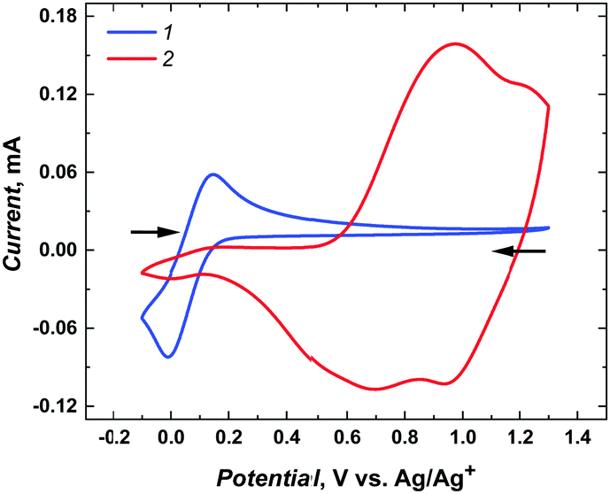
| Fig. 2 The electrochemical responses of (a) poly(meso-NiSaldMe) and (b) poly(NiSaltMe) (1) deposited as continuous polymer films on bare ITO, and (2) mesoporous silica channels located over ITO after polymerization attempts (Fig. S4, ESI†) recorded, at 2 mV s−1 in a propylene carbonate solution containing 0.1 M TBAPF6. | ||
In contrast, and quite unexpectedly, attempts to electropolymerize meso-NiSaldMe and NiSaltMe inside mesoporous silica channels failed, regardless of whether they were carried out under the potentiodynamic or potentiostatic conditions (Fig. S4, ESI†). Consequently, we observed a current drop instead of a characteristic current increase during electropolymerization attempts of meso-NiSaldMe and NiSaltMe inside oriented mesoporous silica channels. Furthermore, the CV responses recorded in the blank electrolyte solution after the electrodeposition attempts of meso-NiSaldMe and NiSaltMe indicated no redox activity on the film electrode (see red curves in Fig. 2a and b). Slight differences in capacitive currents observed in these responses originated from the hindered shuttling of counter ions inside the mesoporous silica matrix. In particular, applying constant potential conditions during polymerization attempts, thus affecting more hindered counter ion shuttling in the consecutively registered electrochemical response (Fig. 2b).
However, the meso-NiSaldMe and NiSaltMe monomers are known to effectively electropolymerize on bare ITO electrodes,44 and their size is smaller than the mesopore aperture so an explanation has to be found to understand such distinct behavior compared to meso-NiSaldMe-3dMe (see Section 3.3).
The electropolymerization of the meso-NiSaldMe-3dMe monomer inside mesoporous silica channels was slower than that on the bare ITO electrode (compare CV cycles (1st, 2nd, 5th, 10th, 20th, 50th, and 100th) depicted at the same current scale, in the right part of Fig. 1). The reason for different growth rates under similar polymerization conditions can be explained by the involvement of different types of energy transfer mechanisms. During the electropolymerization of meso-NiSaldMe-3dMe inside mesoporous channels, the energy migrates by the thermally-activated hopping mechanism, i.e., through intrachain charge transfer.12 That is, a longer time is needed for reorientation of the polymer backbone growing along the mesopore with dipoles located on neighboring conducting segments oriented as head to tail. This reorientation slows down the polymerization of the meso-NiSaldMe-3dMe monomer under potentiodynamic conditions. Besides, this slower electropolymerization also indirectly confirms the poly(meso-NiSaldMe-3dMe) growth within the nanochannels. The faster polymer growth on the planar ITO is connected with interchain energy migration that significantly speeds up the polymerization of meso-NiSaldMe-3dMe.
3.2 Electrochemical comparison of poly(meso-NiSaldMe-3dMe) electrodeposited inside mesoporous silica channels and continuous poly(meso-NiSaldMe-3dMe) deposited on bare ITO
The associated interchain energy transfer, i.e., the energy hopping between chains or within one conducting polymer segment (in both cases based on the coupling of dipoles oriented side-by-side, so-called Förster transfer),11 is much faster than the intrachain energy transfer. However, such fast polymerization can result in polymer lattice defects, i.e., regions of broken conjugation that shorten the conduction lengths.After deposition of poly(meso-NiSaldMe-3dMe), respectively, on the mesoporous silica modified and bare ITO electrodes and rinsing them with propylene carbonate, both electrodes were transferred to a monomer-free electrolyte solution for electrochemical characterization (Fig. 3). Electrochemically followed charge carrier transport of polymeric semiconductors involves accumulation of charge via counter ion doping and dedoping interactions through the material backbone. Because electron transfer at the electrode (ITO)|semiconductor interface is much faster than counter ion mass transport at the electrolyte solution|semiconductor interface, the scan rate of 2 mV s−1 was purposefully used for better comparison of poly(meso-NiSaldMe-3dMe) wires embedded inside vertical channels of mesoporous silica and the continuous film of the same polymer. Additionally, we were able to eliminate the influence of the too slow counter ion diffusion, i.e., hindered counter ion doping and dedoping at high scan rates. This way, we could observe the evolution of well pronounced and highly doped redox species with minimized resistance originating either from the supporting electrolyte solution or from the insulating mesoporous silica matrix.
 | ||
| Fig. 3 Two different projections of the electrochemical response (a) current vs. potential and (b) current vs. time recorded for poly(meso-NiSaldMe-3dMe). (1) Continuous polymer film deposited on bare ITO and (2) molecular wires deposited inside mesoporous silica channels. | ||
The current–potential curves provided electrochemical and mechanistic information about the types of oxidized polymer forms transporting the charge generated as a consequence of the potential-driven charge transfer processes and counter ion doping occurring at different potentials/energies for distinct molecular packing of the poly(meso-NiSaldMe-3dMe) semiconductor, i.e., the poly(meso-NiSaldMe-3dMe) deposited as wires inside mesoporous silica channels and as a continuous polymer film. The bare as well as the underlying mesoporous silica channeled matrix ITO served as electrode substrates providing extra charge carriers. In both molecular packing types of poly(meso-NiSaldMe-3dMe), the charge transport upon electrochemical doping occurs at specific applied potentials, i.e., when an electrochemical potential of the ITO electrons corresponds to electron affinities (ionization energies) of the Ni2+salen polymer segments forming positively charged conjugated forms of the bisphenolic radical cations – polarons27,30 and bisphenolic cations – bipolarons.43 The first peak characteristic of the initial oxidation and doping appeared at ∼0.57 V vs. Ag/Ag+ for the isolated poly(meso-NiSaldMe-3dMe) chains – molecular wires (Fig. 3a2 and b2, red curve 2, peak position I) in silica channels, and at ∼0.50 V vs. Ag/Ag+ for the continuous poly(meso-NiSaldMe-3dMe) film (Fig. 3a1 and b1, blue curve 1, peak position I). Thus, it seems that more energy is needed to start the conduction process in the mesoporous silica isolated poly(meso-NiSaldMe-3dMe) molecular wires undergoing structure rearrangement changes during electrochemical doping inside mesoporous channels.
The second peak characteristic of intrachain bisphenolic radical cation coupling in silica channeled matrix isolated poly(meso-NiSaldMe-3dMe) wires appeared at ∼0.74 V vs. Ag/Ag+ (Fig. 3a2 and b2, red curve 2, peak position II). The interchain bisphenolic radical cation coupling between neighboring chains of the continuous poly(meso-NiSaldMe-3dMe) film manifested itself as the second peak (Fig. 3a1 and b1, blue curve, peak position II) at ∼0.98 V vs. Ag/Ag+ almost merging with the third peak (Fig. 3a1 and b1, blue curve, peak position III) characteristic of the bisphenolic cation (bipolaron) formation at ∼1.23 V vs. Ag/Ag+. The third peak associated with the bisphenolic cation coupling in silica channeled isolated poly(meso-NiSaldMe-3dMe) molecular wires appeared at ∼1.04 V vs. Ag/Ag+ (Fig. 3a2 and b2, red curve 2, peak position II). Fortunately, the generation of charge transport species in the poly(meso-NiSaldMe-3dMe) molecular wires embedded in silica channels required less energy than that needed for the continuous film.
The maximum conductivity of polymer semiconductors is observed when the amount of oxidized and reduced sites of redox states is equal.58 The same amount of anodic and cathodic charge generated during charge transport, i.e., equal areas under anodic and cathodic waves, reflects in the equal amount of accessible redox sites–charge carriers. Such a balance between the amount of charge transported within oxidation and reduction of the poly(meso-NiSaldMe-3dMe) wires isolated inside mesoporous silica was preserved (Fig. 3a2 and b2), confirming the interest in isolating single polymeric chains from each other. In contrast to the continuous poly(meso-NiSaldMe-3dMe) film (Fig. 3a1 and b1), the number of accessible redox sites–charge carriers is smaller because of charge trapping.7
The EIS spectra analysis provided a closer insight into the electrochemical properties of the mesoporous silica isolated poly(meso-NiSaldMe-3dMe) wires and allowed for their comparison with the properties of a continuous film of poly(meso-NiSaldMe-3dMe). Fig. 4 shows the complex plane impedance plot for the poly(meso-NiSaldMe-3dMe) molecular wires deposited inside mesoporous silica channels (red curves) and continuous film of poly(meso-NiSaldMe-3dMe) (black curves) recorded at constant potentials providing the high level of counter ion doping where the maximum conductivity of the polymer should be revealed.58 Each semicircle observed at the high frequency region of the Nyquist plots (see EIS spectra recorded at 0.9, and 1.0 V in Fig. 4) is characteristic of the charge transfer processes, i.e., heterogeneous redox reactions occurring at the interface of [(ITO electrode)|(mesoporous silica surrounded polymer wires) – red curves], and [(ITO electrode)|(continuous polymer) – black curves], respectively, simultaneously with the double layer charging in both cases.
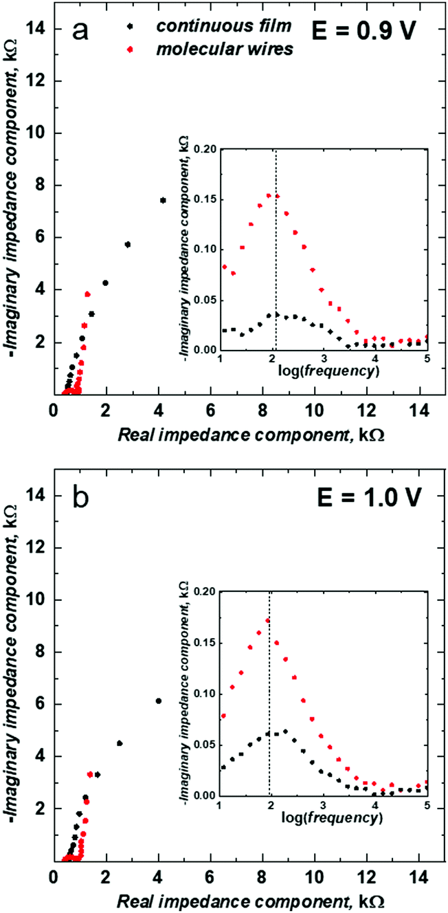 | ||
| Fig. 4 The comparative Nyquist plots and Debye plots (in insets) for poly(meso-NiSaldMe-3dMe) deposited on the bare ITO electrode as a continuous film (black dots) and molecular wires deposited inside mesoporous silica channels oriented over ITO (red dots). EIS measurements were recorded in a propylene carbonate solution of 0.1 M (TBA)PF6, for constant potentials of (a) 0.9 and (b) 1.0 V. Before the EIS measurements, each electrode was equilibrated by applying the selected potential for 30 s. After this time, the current reached equilibrium, and then EIS measurements were performed with the voltage amplitude of 10 mV in the frequency range of 100 kHz to10 mHz. | ||
The presence of semicircles at high doping levels of poly(meso-NiSaldMe-3dMe) wires confirmed their successful deposition inside mesoporous silica channels and the possibility of electron mediation through such molecular interconnections. Diameters of semicircles observed for poly(meso-NiSaldMe-3dMe) wires embedded inside silica channels were broader than those observed for ITO coated with a continuous polymer film. Presumably, it indicated on an increasing impact of double-layer charging occurring simultaneously with redox reactions for poly(meso-NiSaldMe-3dMe) wires deposited inside silica channels. However, resistances observed at the low frequency region of the Nyquist plot (related to the imaginary and real impedance values) associated with diffusional processes are lower for silica isolated poly(meso-NiSaldMe-3dMe) wires.
In order to compare conductivity relaxation times inside the channels of a dielectric material filled with poly(meso-NiSaldMe-3dMe) wires and the continuous poly(meso-NiSaldMe-3dMe) film, we plotted the imaginary impedance as a function of frequency, i.e., the Debye plot59 (see insets in Fig. 4). The characteristic of the conductivity relaxation is reflected in the Debye peak maxima.60 It can be seen that the peak maxima appeared at the same position indicating a similar conductivity relaxation time inside the channels of dielectric silica filled with poly(meso-NiSaldMe-3dMe) wires and the continuous poly(meso-NiSaldMe-3dMe) film at a high level of counter ion doping.58
In addition, a permeability test with the decamethylferrocene redox probe confirmed that mesoporous silica channels were filled with poly(meso-NiSaldMe-3dMe) wires. Indeed, in addition to the polymer signals in the 0.4–1.2 V vs. Ag/Ag+ region, only a feeble signal from the redox probe was observed at 0.1 V vs. Ag/Ag+ compared to the intense and well-defined one on the same electrode before the deposition of poly(meso-NiSaldMe-3dMe) wires (Fig. 5).
 | ||
| Fig. 5 CV curves recorded at 20 mV s−1 in the propylene carbonate solution containing 1 mM bis(pentamethylcyclopentadienyl)iron solution and 0.1 M TBAPF6 for (1) the ITO electrode with vertical open silica channels (after CTAB extraction) and (2) the poly(meso-NiSaldMe-3dMe) wires deposited inside silica channels. | ||
3.3 Structural requirements of nickel salen monomers for their deposition inside the mesoporous silica channels
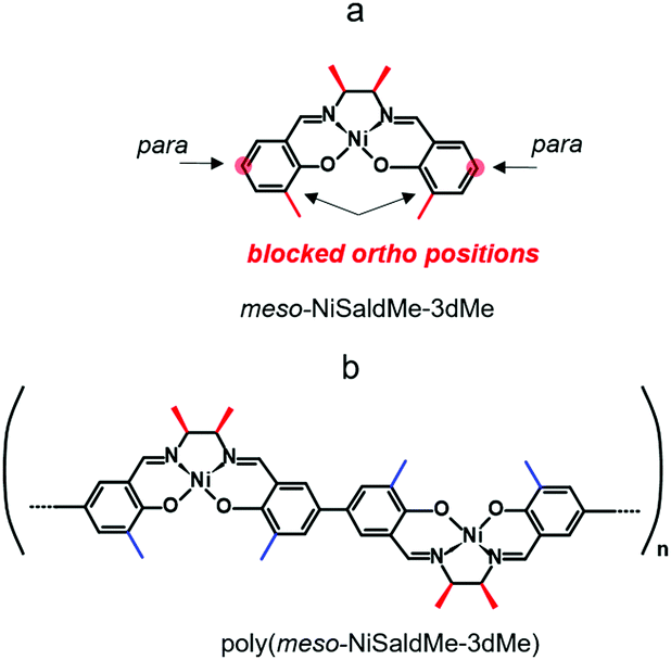
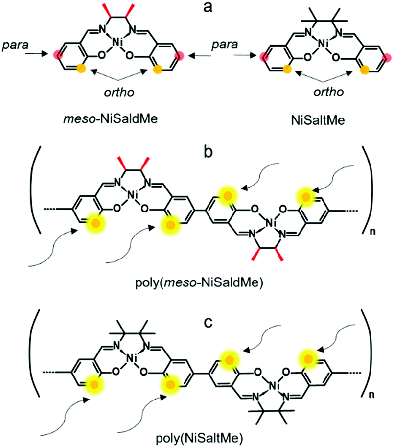
Our former goal was to extend the potential range of electroactivity of Ni2+salen polymers without affecting their electrochemical stability, for which the new analog of meso nickel salen monomer, viz., meso-N,N′-bis-(3-methylosalicylidene)-2,3-butanediaminonickel, abbreviated as meso-NiSaldMe-3dMe was synthesized (Scheme 2a).44 This particular meso Ni2+salen monomer has both 3-positions of the salicylaldehyde moieties substituted with methyl, and it is able to form a continuous poly(meso-NiSaldMe-3dMe) film (Scheme 2b) in the course of electrooxidation. It was proved by computational modelling and spectroelectrochemical experiments that the privileged and primary bonding places for Ni2+salen are para positions between two anti-parallel monomer units.43 However, the linear chain elongation in the direction of increasing conjugation in the –O![[double bond, length as m-dash]](https://www.rsc.org/images/entities/char_e001.gif) PhPhO–(Ni)–OPhPh–O– direction can be interrupted by fast and incidental cation radicals pairing at ortho positions for ortho unsubstituted Ni2+salens (Scheme 3a).
PhPhO–(Ni)–OPhPh–O– direction can be interrupted by fast and incidental cation radicals pairing at ortho positions for ortho unsubstituted Ni2+salens (Scheme 3a).
 | ||
| Scheme 2 Structural formulas of (a) meso-NiSaldMe-3dMe monomer and (b) poly(meso-NiSaldMe-3dMe) polymer. | ||
 | ||
| Scheme 3 Structural formulas of (a) meso-NiSaldMe monomer, (b) NiSaltMe monomer, (c) poly(meso-NiSaldMe) polymer, and (d) poly(NiSaltMe) polymer. | ||
Notably, the elongation of the poly(meso-NiSaldMe-3dMe) (Scheme 2b) chain can be exclusively linear because methyl substituents block both 3-positions of each salicylaldehyde moiety (ortho positions). When ortho positions of Ni2+salen monomers are not substituted, for example, in the monomers shown in Scheme 3a the polymer chain branching can occur (Scheme 3b and c).
The role of methyl substituents at the 3-positions of each salicylaldehyde moiety of the poly(meso-NiSaldMe-3dMe) is to increase the electron density in the charge conduction direction, i.e., along the –OPhPhO–(Ni)–OPhPh–O– conduction path.27 Furthermore, we anticipate that this linear conjugation increase in the –OPhPhO–(Ni)–OPhPh–O– direction enables straightening of the poly(meso-NiSaldMe-3dMe) chains and by this facilitates local deposition inside mesoporous silica channels.
In contrast, the high electron density concentration at ortho and para positions of unsubstituted meso-NiSaldMe and NiSaltMe monomers resulted in the possibility of bond formation between units at more than one place during polymerization. Most probably, this branching feature is the origin of their restricted electrodeposition through the mesoporous silica film.
A more detailed explanation of this phenomenon came from computational modeling results. The dimensions of optimized structures of meso-NiSaldMe-3dMe, meso-NiSaldMe, and NiSaltMe (Fig. 6) and their energetically stable π-stacked dimers were determined (Fig. 7). It was revealed that all three monomers and their corresponding anti-parallel π–π stacked dimers are not size-excluded because their crucial dimensions (Fig. 6 and 7) are smaller than the pore aperture (2 nm).16 Only the meso-NiSaldMe-3dMe monomer can be polymerized inside mesopores; one cannot use the size exclusion criteria to explain such differences. However, the probability of the π–π interactions between two Ni2+salen monomers in pre-polymerization solution has to be considered (Fig. 7) especially because of their negligible planarity deviation.
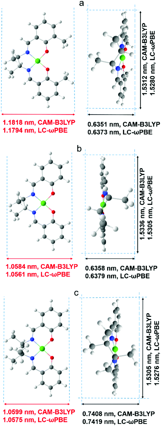 | ||
| Fig. 6 Approximate dimensions with the van der Waals radii taken into account determined for molecular structures of (a) meso-NiSaldMe-3dMe, (b) meso-NiSaldMe, and (c) NiSaltMe, optimized with the use of two functionals: CAM-B3LYP and LC-ωPBE. The dimensions of monomers that are crucial from the point of view of molecular sieving properties of mesoporous silica channels are marked in red. | ||
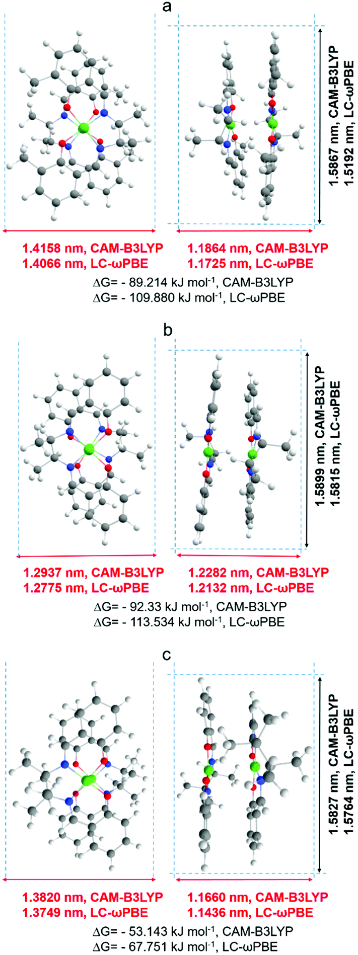 | ||
| Fig. 7 Approximate dimensions with the van der Waals radii taken into account and the Gibbs energy values determined for molecular structures of the anti-parallel π–π stack dimers of (a) meso-NiSaldMe-3dMe, (b) meso-NiSaldMe, and (c) NiSaltMe optimized with the use of two functionals: CAM-B3LYP and LC-ωPBE. The dimensions of dimers that are crucial from the point of view of molecular sieving properties of mesoporous silica channels are marked in red. | ||
We anticipate that mesopores are filled with energetically stable anti-parallel π–π stacks of Ni2+salen monomers before the potential required to start the electropolymerization is applied. Then, when the required potential is reached, the π–π stacked dimers placed in close vicinity of the electrode surface are oxidized, i.e., two repulsive cation radicals are formed as a result of electron removal. Thus, two oxidized components of a π–π stack dimer placed in the mesoporous channel are sliding with consequent rearrangements and pairing cation radicals to form a bond close to the nearest electron-rich positions (Fig. S7a and Video file a, ESI†). These nearest electron-rich positions were identified based on the Mulliken charges determined from DFT optimized structures (Fig. S5 and S6, ESI†).
The values of Mulliken charges determined for the meso-NiSaldMe-3dMe monomer and its anti-parallel π–π stack dimer (Fig. S5a and S6a, ESI†) demonstrated that the bonding between anti-parallel polymer units occurred between two para positions (Fig. S7a and Video file a, ESI†). Moreover, the crucial dimension for deposition in mesopores of linearly elongated anti-parallel poly(meso-NiSaldMe-3dMe) is 1.36 nm (Scheme 4a). The values of Mulliken charges determined for meso-NiSaldMe, and NiSaltMe monomers and their anti-parallel π–π stack dimers, respectively (Fig. S5b, c and S6b, c, ESI†), demonstrated that the bonding between anti-parallel polymer units occurred between ortho–para and para–para positions.
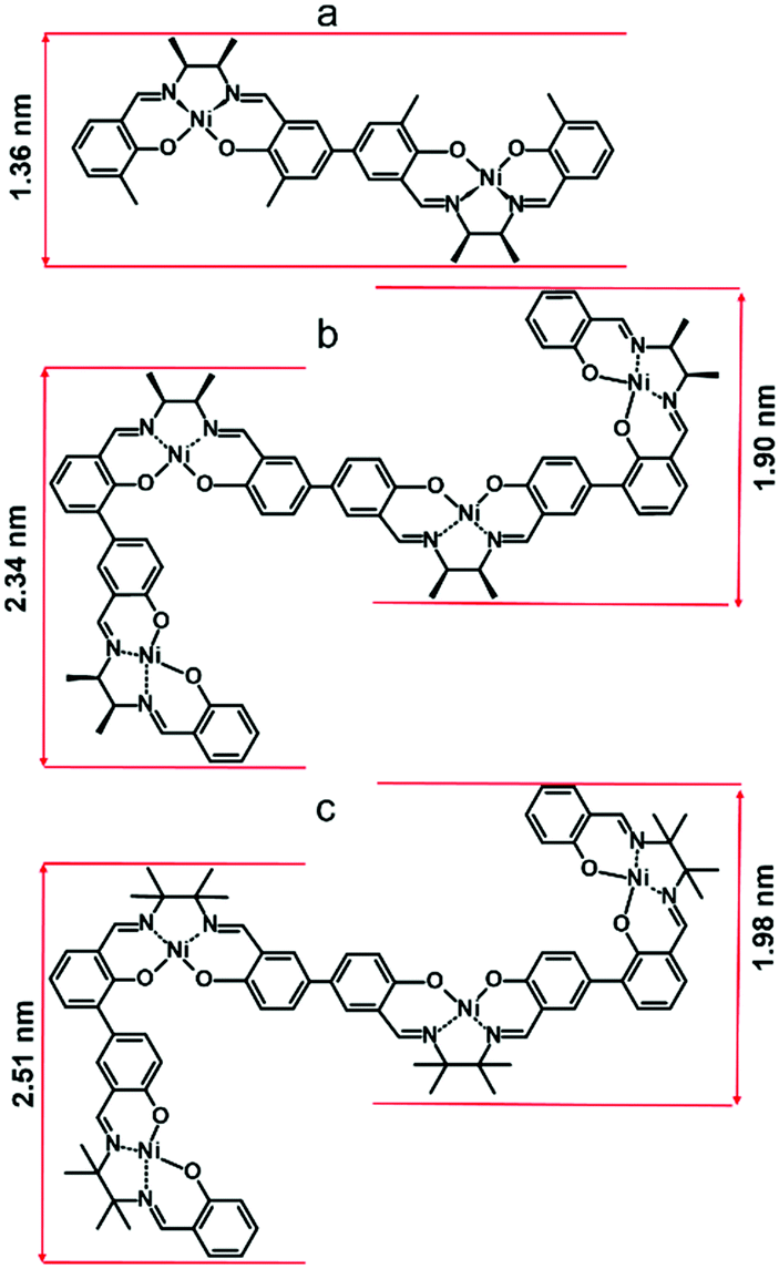 | ||
| Scheme 4 The dimensions of the linearly elongated (a) poly(meso-NiSaldMe-3dMe) and the branched structures of (b) poly(meso-NiSaldMe) and (c) poly(NiSaltMe) polymers. | ||
The possibility of bonding at ortho–para positions observed for poly(meso-NiSaldMe) and poly(NiSaltMe), respectively (Fig. S7b and c, Video file b and c, ESI†), determined their branching properties. The proposed branched structures of poly(meso-NiSaldMe) and poly(NiSaltMe) (Scheme 4b and c) have dimensions larger than 2 nm, evidencing that they are most likely size excluded from silica channels, i.e., branched poly(meso-NiSaldMe) and poly(NiSaltMe) cannot be formed inside the silica channel. This exclusion could explain the marked difference in reactivity when attempting to electropolymerize the three monomers in spatially confined environments. Notably, only the bottom of the silica channeled template, i.e., ITO substrate, is conducting. Ni2+salen monomers are capable of electropolymerization only on conducting electrode surfaces. The meso-NiSaldMe and NiSaltMe can diffuse through 2 nm in diameter vertical channels to reach the underlying polarized ITO substrate. These monomers can be oxidized but not polymerized because of charge distribution features enabling exclusively linear elongation of the polymer needed for deposition inside mesoporous channels. Therefore, the process stops at monomer oxidation at the bottom of silica channels, and no polymerization occurs at the silica surface.‡
3.4 Microscopic and spectroscopic evidence of molecular level isolation of poly(meso-NiSaldMe-3dMe) wires inside mesoporous silica channels
Visualizing the mesoporous silica channel matrix structure with poly(meso-NiSaldMe-3dMe) molecular wires confined inside by TEM (Fig. 8) confirmed that the electropolymerization process did not damage the regular hexagonally packed matrix nanostructure. This is evident from both the top views revealing the hexagonal packing of channels 2.0 nm in diameter surrounding the poly(meso-NiSaldMe-3dMe) molecular wires (Fig. 8A) and the cross-sections exhibiting uniform thickness of vertically aligned nanochannels of 85 nm length isolating molecular wires (Fig. 8A). The observed diameters of vertical and hexagonally packed mesoporous silica channels are characteristic of the EASA preparation method utilizing the CTAB surfactant.16 The hexagonally packed structure of the silica matrix has been ideally preserved because the width diameter of the poly(meso-NiSaldMe-3dMe) molecular wires confined inside is below 2 nm. The molecular wire width dimensions are below 1.5 nm, as indicated by diameters extracted from optimized molecular structures (Fig. 7a). Moreover, the dimension of the dopant – hexafluorophosphate anion is 0.508 nm, thus confirming that molecular wire width remains within (2–0.508 nm).56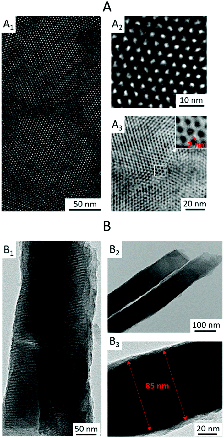 | ||
| Fig. 8 Transmission electron micrographs obtained at various magnifications of the poly(meso-NiSaldMe-3dMe) molecular wires deposited inside mesoporous silica channels presented as (A) top views where (A1–A3) enable evaluation of the pore diameter, and (B) cross-sectional views where (B1–B3) enable evaluation of the film thickness. | ||
Another, yet indirect, piece of evidence of successful deposition of poly(meso-NiSaldMe-3dMe) inside the channels of the mesoporous silica matrix was obtained from AFM via energy dissipation measurements with the PeakForce QNM mode. AFM allows for local mapping of the nanomechanical properties of the silica isolated wire surface, based on different plastic deformation of both [silica and poly(meso-NiSaldMe-3dMe)] components. Our measurements revealed a bimodal distribution in mechanical dissipation values correlated to the spatial distribution of silica surrounded molecular wires. The observed nanomechanical dissipation is bigger for the more plastic/elastic poly(meso-NiSaldMe-3dMe) conducting polymer wire (mapped in white and yellow in Fig. 9) and smaller for the more rigid/stiff silica matrix (mapped in orange and brown in Fig. 9). However, the appearance of the small patches of high dissipation energy randomly distributed over a low dissipation energy background indicated the limitations of this technique. This range is relatively larger than the size of the pores in the silica matrix and can be related to resolution limitations due to the AFM-tip apex size.
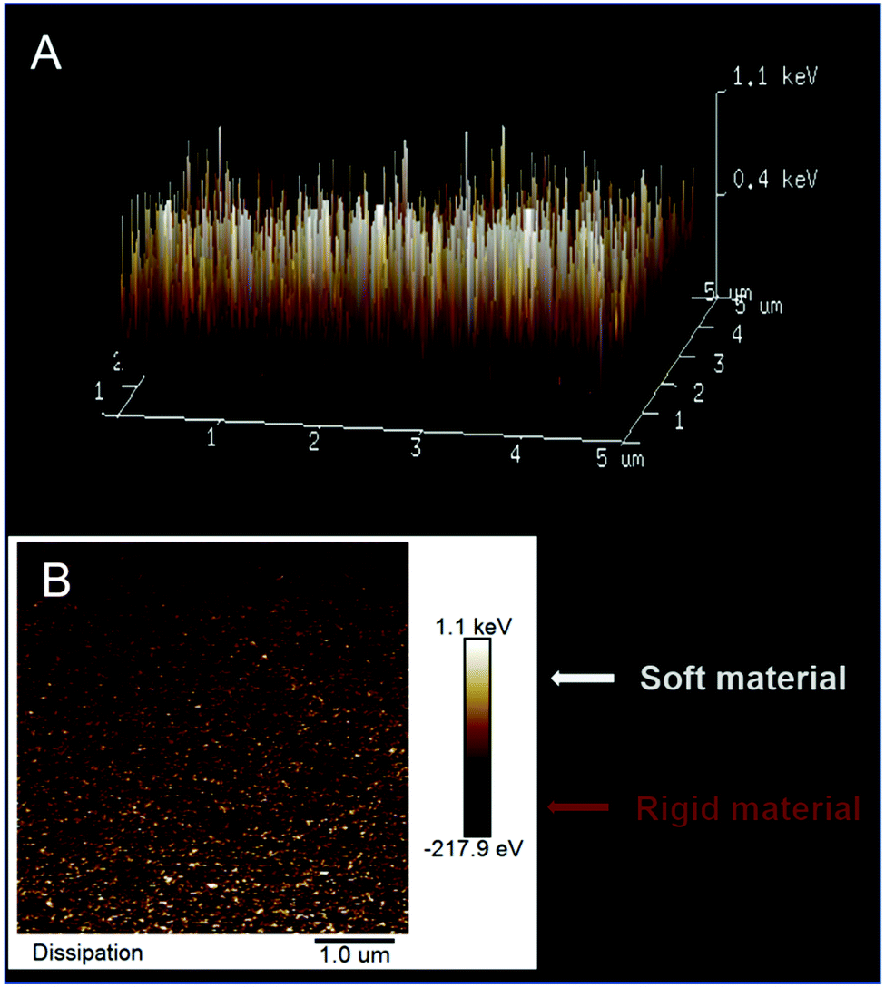 | ||
| Fig. 9 The AFM energy dissipation maps (A) in 3D and (B) in 1D of poly(meso-NiSaldMe-3dMe) wires deposited inside mesoporous silica channels (white and yellow polymer wires, orange and brown mesoporous silica channel matrix). | ||
Finally, the high-resolution XPS was combined with very low energy argon ion Ar+ beam sputtering for depth-profile chemical analysis of the poly(meso-NiSaldMe-3dMe) molecular wires confined inside the mesoporous silica channels. Fig. 10 shows the variation of relative contents of Ni, C, and Si, measured after Ar+ ion etching. The high-resolution XPS spectra of Ni(2p), C(1s) and Si(2p) were recorded at the depths of ∼11.2 nm, ∼13.44 nm, ∼15.58 nm, and ∼17.92 nm, after sputter times ranging from 10 to 16 min, demonstrating a uniform depth distribution of the poly(meso-NiSaldMe-3dMe) wires inside the silica matrix. This definitely proved the presence of the polymer molecular wires inside the silica channels. Moreover, the Ni(2p) signal characteristic of the retained square-planar geometry of Ni2+,61 preserved even after Ar+ ion etching (Fig. S8, ESI†) indicated the presence of single polymer wires inside silica channels, as multiple chain deposits would have resulted in deviation from the square-planar geometry of Ni2+inside the channels. Furthermore, the constant concentration profile of Ni2+ also corroborates the above hypothesis of elongated single polymer chains deposited in the nanochannels because of the lack of progressive enrichment of the polymer content as it grew in the mesoporous channels. Typical XPS spectra recorded before and after sputtering are shown in Fig. S8 (ESI†) (Ni 2p, C 1s, and Si 2p core levels, but also N 1s and O 1s). By integrating these signals, one can estimate a N/Ni atomic ratio of 2.2 after sputtering, which is close to the expected value of 2 based on the stoichiometry of the Ni2+salens. The calculated C/Ni ratio of 27 is more than the expected one (20), and the overvaluation probably originates from some remaining ethoxy groups in the mesoporous silica film.62,63
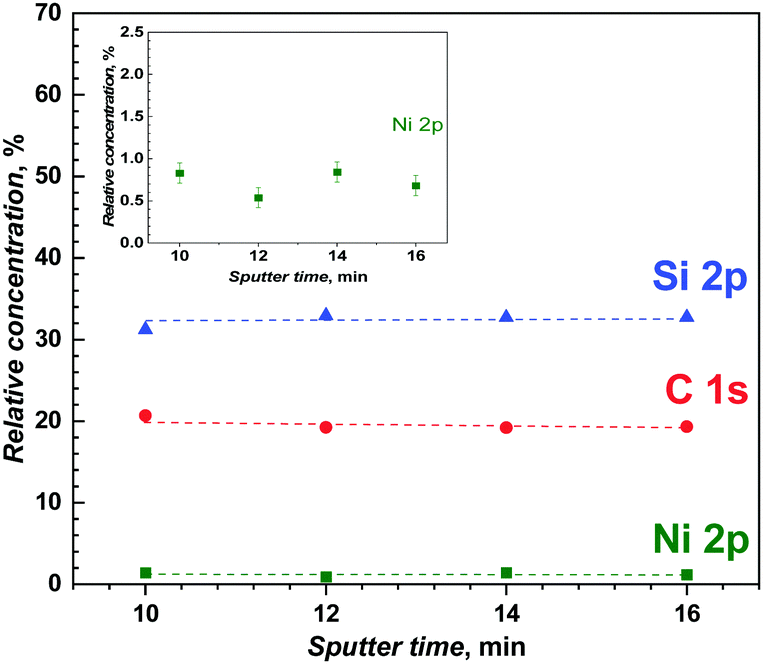 | ||
| Fig. 10 Variation of the relative concentrations of Ni 2p, Si 2p and C 1s obtained from the depth-profiling chemical analysis of the poly(meso-NiSaldMe-3dMe) molecular wires deposited inside mesoporous silica channels, for various times of energy argon ion beam sputtering (500 V, 2 × 2 mm, sputter rate: 1.12 nm min−1). Inset: enlargement of the Ni 2p data. Concentrations of Ni 2p, Si 2p and C 1s were measured after the argon ion Ar+ beam profiling at the depths of ∼11.2 nm, ∼13.44 nm, ∼15.58 nm, and ∼17.92 nm. | ||
4. Conclusions
This work demonstrated that when attempting to electropolymerize three structurally different nickel salens: meso-NiSaldMe-3dMe, meso-NiSaldMe, and NiSaltMe, equally able to form continuous poly(Nisalen) films on bare ITO, only one of these monomers can be electropolymerized inside mesoporous silica channels of 2 nm in diameter. These monomers and their anti-parallel π–π stack dimers possess similar sizes, lower than the mesopore aperture, thus they are not excluded from the mesoporous silica channels because of their dimensions. Still, meso-NiSaldMe and NiSaltMe monomers could not polymerize inside the mesoporous silica matrix because the aromatic part of these monomers possessed a free ortho position determining the possibility of poly(NiSalen)s branching. By contrast, the presence of two moderately electron-donating methyl substituents at the ortho position of the aromatic part of the meso-NiSaldMe-3dMe determined its ability for electropolymerization in the mesoporous silica channels. Because of the blocking of the ortho position, there was no possibility of polymer branching, which ultimately restricted the meso-NiSaldMe-3dMe molecular wire dimensions below the mesoporous channel diameter.Once formed inside the nanochannels, the poly(meso-NiSaldMe-3dMe) molecular wires are well separated from each other because of the presence of silica walls, thus preventing the interactions between the individual polymer chains causing charge carrier trapping and interchain energy flow through space between neighboring chains. This separation resulted in enhanced charge transport properties of poly(meso-NiSaldMe-3dMe) molecular wires compared to those of the poly(meso-NiSaldMe-3dMe) continuous film. This research made it possible to understand how to control the charge transport in Ni2+salen polymers by tuning their structure at the molecular level (by combining the use of a mesoporous silica matrix of open channels and suitably tuned molecular structures of Ni2+salens) responsible for the isolation of their intrinsic charge propagation processes that are critical for molecular interconnections transporting energy to desired locations with a minimum loss. Furthermore, the results of our studies revealed that polymerization of Ni2+salens occurs by covalent bonding between para positions in ortho substituted monomers, or between para and ortho positions in phenyl ring unsubstituted Ni2+salens. Markedly, if the polymerization mechanism of Ni2+salens was based on non-covalent stacking, all nickel salen monomers that are not size excluded from the 2 nm channel would polymerize in such a matrix.
Conflicts of interest
The authors declare no conflicts of interest.Acknowledgements
We thank Dr Neus Vila (LCPME CNRS) for the help with the TEM measurements, and Prof. Wojciech Lisowski (Institute of Physical Chemistry, Polish Academy of Sciences) for the XPS depth-profiling measurements. Kamila Łępicka would like to thank LCPME CNRS (France) for the opportunity to establish international cooperation under ETIUDA 6 pre-postdoctoral Travel-Grant No. 2018/28/T/ST5/00131 (KŁ) of the National Science Center (Poland). The present research was financially supported by the National Science Center (Poland) through Grant OPUS 15 No. 2018/29/B/ST5/02335 (PSS).Notes and references
- F. S. Kim, G. Ren and S. A. Jenekhe, Chem. Mater., 2011, 23, 682–732 CrossRef CAS.
- Y.-Z. Long, M. Li, C. Gu, M. Wan, J. Duvail, Z. Liu and Z. Fan, Prog. Polym. Sci., 2011, 36, 1415–1442 CrossRef CAS.
- T.-Q. Nguyen, J. Wu, S. H. Tolbert and B. J. Schwartz, Adv. Mater., 2001, 13, 609–611 CrossRef CAS.
- T. Kitao, S. Bracco, A. Comotti, P. Sozzani, M. Naito, S. Seki, T. Uemura and S. Kitagawa, J. Am. Chem. Soc., 2015, 137, 5231–5238 CrossRef CAS PubMed.
- J. Ackermann, C. Videlot, T. N. Nguyen, L. Wang, P. M. Sarro, D. Crawley, K. Nikolić and M. Forshaw, Appl. Surf. Sci., 2003, 212-213, 411–416 CrossRef CAS.
- A. Gamero-Quijano, C. Karman, N. Vilà, G. Herzog and A. Walcarius, Langmuir, 2017, 33, 4224–4234 CrossRef CAS PubMed.
- H. F. Haneef, A. M. Zeidell and O. D. Jurchescu, J. Mater. Chem. C, 2020, 8, 759–787 RSC.
- A. Walcarius, Chem. Soc. Rev., 2013, 42, 4098–4140 RSC.
- S. Lhenry, J. Jalkh, Y. R. Leroux, J. Ruiz, R. Ciganda, D. Astruc and P. Hapiot, J. Am. Chem. Soc., 2014, 136, 17950–17953 CrossRef CAS PubMed.
- S. Bracco, A. Comotti, L. Ferretti and P. Sozzani, J. Am. Chem. Soc., 2011, 133, 8982–8994 CrossRef CAS PubMed.
- T. Förster, Ann. Phys., 2006, 437, 55–75 CrossRef.
- B. J. Schwartz, T.-Q. Nguyen, J. Wu and S. H. Tolbert, Synth. Met., 2001, 116, 35–40 CrossRef CAS.
- J. Wu, A. F. Gross and S. H. Tolbert, J. Phys. Chem. B, 1999, 103, 2374–2384 CrossRef CAS.
- A. Walcarius, E. Sibottier, M. Etienne and J. Ghanbaja, Nat. Mater., 2007, 6, 602–608 CrossRef CAS PubMed.
- A. Goux, M. Etienne, E. Aubert, C. Lecomte, J. Ghanbaja and A. Walcarius, Chem. Mater., 2009, 21, 731–741 CrossRef CAS.
- N. Vilà, E. André, R. Ciganda, J. Ruiz, D. Astruc and A. Walcarius, Chem. Mater., 2016, 28, 2511–2514 CrossRef.
- A. Goux, J. Ghanbaja and A. Walcarius, J. Mater. Sci., 2009, 44, 6601–6607 CrossRef CAS.
- L. Ding, W. Li, Q. Wang, Q. Sun, Y. He and B. Su, Chem. – Eur. J., 2014, 20, 1829–1833 CrossRef CAS PubMed.
- L. Ding and B. Su, J. Electroanal. Chem., 2015, 736, 83–87 CrossRef CAS.
- N. R. Chiou, C. Lu, J. Guan, L. J. Lee and A. J. Epstein, Nat. Nanotechnol., 2007, 2, 354–357 CrossRef CAS.
- T.-Q. Nguyen, V. Doan and B. J. Schwartz, J. Chem. Phys., 1999, 110, 4068–4078 CrossRef CAS.
- M. A. del Valle, M. Gacitúa, F. R. Díaz, F. Armijo and R. D. Río, Electrochem. Commun., 2009, 11, 2117–2120 CrossRef CAS.
- F. Qu, H. Sun, Y. Zhang, H. Lu and M. Yang, Sens. Actuators, B, 2012, 166-167, 837–841 CrossRef CAS.
- W. Ullah, G. Herzog, N. Vilà and A. Walcarius, Electrochem. Commun., 2021, 122, 106896 CrossRef CAS.
- A. Kapturkiewicz and B. Behr, Inorg. Chim. Acta, 1983, 69, 247–251 CrossRef CAS.
- T. Hirao, Coord. Chem. Rev., 2002, 226, 81–91 CrossRef CAS.
- M. Vilas-Boas, C. Freire, B. de Castro, P. A. Christensen and A. R. Hillman, Inorg. Chem., 1997, 36, 4919–4929 CrossRef CAS.
- B. Akinwolemiwa, C. Wei and G. Z. Chen, Electrochim. Acta, 2017, 247, 344–357 CrossRef CAS.
- E. V. Anslyn and D. A. Dougherty, Modern Physical Organic Chemistry, American Chemical Society, Sausalito, California, 2006, ch. 17, pp. 1016–1022 Search PubMed.
- M. Vilas-Boas, C. Freire, B. de Castro, P. A. Christensen and A. R. Hillman, Chem. – Eur. J., 2001, 7, 139–150 CrossRef CAS PubMed.
- M. Vilas-Boas, C. Freire, B. de Castro and A. R. Hillman, J. Phys. Chem. B, 1998, 102, 8533–8540 CrossRef CAS.
- M. Nunes, M. Araujo, J. Fonseca, C. Moura, R. Hillman and C. Freire, Appl. Mater. Interfaces, 2016, 8, 14231–14243 CrossRef CAS PubMed.
- G. Yan, J. Li, Y. Zhang, F. Gao and F. Kang, J. Phys. Chem. C, 2014, 118, 9911–9917 CrossRef CAS.
- J. L. Bott-Neto, T. S. Martins, S. A.-S. Machado and E. A. Ticianelli, Appl. Mater. Interfaces, 2019, 11, 30810–30818 CrossRef CAS PubMed.
- C. E. Dahm, D. G. Peters and J. Simonet, J. Electroanal. Chem., 1996, 410, 163–171 CrossRef.
- G. A. Shagisultanova and N. N. Kuznetsova, Russ. J. Coord. Chem., 2003, 29, 703–709 CrossRef CAS.
- T. Y. Rodyagina, P. V. Gaman'kov, E. A. Dmitrieva, I. A. Chepurnaya, S. V. Vasil'eva and A. M. Timonov, Russ. J. Electrochem., 2005, 41, 1101–1110 CrossRef CAS.
- S. V. Vasileva, K. P. Balashev and A. M. Timonov, Russ. J. Electrochem., 2000, 36, 75–79 CrossRef CAS.
- C. Friebe, M. D. Hager, A. Winter and U. S. Schubert, Adv. Mater., 2012, 24, 332–345 CrossRef CAS PubMed.
- E. V. Alekseeva, I. A. Chepurnaya, V. V. Malev, A. M. Timonov and O. V. Levin, Electrochim. Acta, 2017, 225, 378–391 CrossRef CAS.
- M. P. Karushev and A. M. Timonov, Russ. J. Appl. Chem., 2012, 85, 914–920 CrossRef CAS.
- K. Łępicka, P. Pieta, R. Gupta, M. Dabrowski and W. Kutner, Electrochim. Acta, 2018, 268, 111–120 CrossRef.
- K. Łępicka, P. Pieta, A. Shkurenko, P. Borowicz, M. Majewska, M. Rosenkranz, S. Avdoshenko, A. A. Popov and W. Kutner, J. Phys. Chem. C, 2017, 121, 16710–16720 CrossRef.
- K. Łępicka, P. Pieta, G. Francius, A. Walcarius and W. Kutner, Electrochim. Acta, 2019, 315, 75–83 CrossRef.
- K. Łępicka, M. Majewska, R. Nowakowski, W. Kutner and P. Pieta, Electrochim. Acta, 2019, 297, 94–100 CrossRef.
- J. F. Dobson and T. Gould, J. Phys.: Condens. Matter, 2012, 24, 073201 CrossRef PubMed.
- S. Grimme, J. Antony, S. Ehrlich and H. Krieg, J. Chem. Phys., 2010, 132, 154104 CrossRef PubMed.
- J. J. Stewart, J. Mol. Model., 2007, 13, 1173–1213 CrossRef CAS PubMed.
- J. J. P. Stewart, Stewart Computational Chemistry, http://OpenMOPAC.net.
- T. Tsuneda and T. Taketsugu, in π-Stacked Polymers and Molecules: Theory, Synthesis, and Properties, ed. T. Nakano, Springer, Japan, Tokyo, 2014, pp. 245–270 DOI:10.1007/978-4-431-54129-5_5.
- T. Yanai, D. P. Tew and N. C. Handy, Chem. Phys. Lett., 2004, 393, 51–57 CrossRef CAS.
- O. A. Vydrov and G. E. Scuseria, J. Chem. Phys., 2006, 125, 234109 CrossRef PubMed.
- M. J. Frisch, G. W. Trucks, H. B. Schlegel, G. E. Scuseria, M. A. Robb, J. R. Cheeseman, G. Scalmani, V. Barone, G. A. Petersson, H. Nakatsuji, X. Li, M. Caricato, A. V. Marenich, J. Bloino, B. G. Janesko, R. Gomperts, B. Mennucci, H. P. Hratchian, J. V. Ortiz, A. F. Izmaylov, J. L. Sonnenberg, D. Williams-Young, F. Ding, F. Lipparini, F. Egidi, J. Goings, B. Peng, A. Petrone, T. Henderson, D. Ranasinghe, V. G. Zakrzewski, J. Gao, N. Rega, G. Zheng, W. Liang, M. Hada, M. Ehara, K. Toyota, R. Fukuda, J. Hasegawa, M. Ishida, T. Nakajima, Y. Honda, O. Kitao, H. Nakai, T. Vreven, K. Throssell, J. A. Montgomery Jr., J. E. Peralta, F. Ogliaro, M. J. Bearpark, J. J. Heyd, E. N. Brothers, K. N. Kudin, V. N. Staroverov, T. A. Keith, R. Kobayashi, J. Normand, K. Raghavachari, A. P. Rendell, J. C. Burant, S. S. Iyengar, J. Tomasi, M. Cossi, J. M. Millam, M. Klene, C. Adamo, R. Cammi, J. W. Ochterski, R. L. Martin, K. Morokuma, O. Farkas, J. B. Foresman and D. J. Fox, Gaussian 16 Search PubMed , Wallingford, CT, 2016.
- R. C. Roy, R. Bhattacharjya and D. K. Das, Indian J. Chem., Sect. A: Inorg., Bio-inorg., Phys., Theor. Anal. Chem., 2004, 43A, 1689–1691 CAS.
- P. S. Kumar and V. Lakshminarayanan, Langmuir, 2007, 23, 1548–1554 CrossRef CAS PubMed.
- M. Inagaki, H. Konno and O. Tanaike, J. Power Sources, 2010, 195, 7880–7903 CrossRef CAS.
- C. Karman, N. Vilà and A. Walcarius, ChemElectroChem, 2016, 3, 2130–2137 CrossRef CAS.
- J. Heinze, B. A. Frontana-Uribe and S. Ludwigs, Chem. Rev., 2010, 110, 4724–4771 CrossRef CAS PubMed.
- J. R. Macdonald, Impedance Spectroscopy, 1991, pp. 283–287 Search PubMed.
- I. M. Hodge, M. D. Ingram and A. R. West, J. Electroanal. Chem., 1976, 74, 125–143 CrossRef CAS.
- J. Matienzo, L. I. Yin, S. O. Grim and W. E. Swartz, Inorg. Chem., 1973, 12, 2762–2769 CrossRef CAS.
- S. Ahoulou, N. Vilà, S. Pillet, D. Schaniel and A. Walcarius, Chem. Mater., 2019, 31, 5796–5807 CrossRef CAS.
- M. Laird, C. Carcel, E. Oliviero, G. Toquer, P. Trens, J. R. Bartlett and M. Wong Chi Man, Microporous Mesoporous Mater., 2020, 297, 110042 CrossRef CAS.
Footnotes |
| † Electronic supplementary information (ESI) available: CV curves obtained for the mesoporous silica channel matrix characterization in the presence of a decamethylferrocene redox probe; CV curves obtained for the mesoporous silica channel matrix characterization at different potential scan rates in a supporting electrolyte solution; Nyquist plots prepared based on EIS measurements obtained for mesoporous silica channel matrix in a supporting electrolyte solution at different potentials; the oxidative electropolymerization attempts of meso-NiSaldMe and NiSaltMe inside mesoporous silica channels; the values of Mulliken charges determined from DFT calculations; the preferential bonding placement between anti-parallel polymer units for meso-NiSaldMe-3dMe, meso-NiSaldMe, and NiSaltMe; XPS spectra obtained for poly(meso-NiSaldMe-3dMe) molecular wires deposited inside mesoporous silica channels before and after the low energy argon ion beam sputtering. See DOI: https://doi.org/10.1039/d2tc00976e |
| ‡ Animations/Videos (Animations showing the preferential bonding placement between anti-parallel units for (Video file a) – poly(meso-NiSaldMe-3dMe), (Video file b) – poly(meso-NiSaldMe), and (Video file a) – poly(NiSaltMe). |
| This journal is © The Royal Society of Chemistry 2022 |