
 Open Access Article
 This Open Access Article is licensed under a
 Creative Commons Attribution 3.0 Unported Licence
Air stable eco-friendly quantum dots with a light-mediated photoinitiator for an inkjet printed flexible light emitting diode†
Hanleem
Lee
,
Yo-Han
Suh
 ,
Xiang-Bing
Fan
,
Limeng
Ni
,
Jiajie
Yang
,
Yoonwoo
Kim
,
Jeong-Wan
Jo
,
Hyung Woo
Choi
,
Sung-Min
Jung
,
Dong-Wook
Shin
*,
Sanghyo
Lee
* and
Jong Min
Kim
,
Xiang-Bing
Fan
,
Limeng
Ni
,
Jiajie
Yang
,
Yoonwoo
Kim
,
Jeong-Wan
Jo
,
Hyung Woo
Choi
,
Sung-Min
Jung
,
Dong-Wook
Shin
*,
Sanghyo
Lee
* and
Jong Min
Kim
Department of Electrical Engineering, University of Cambridge, 9 JJ Thomson Avenue, CB3 0FA, UK. E-mail: ds887@cam.ac.uk; sl920@cam.ac.uk
First published on 29th June 2022
Abstract
Printed quantum dot (QD) light emitting diodes (QLEDs) over a large scale have received much interest in the last decade owing to the demand for the next generation of self-emissive large-area displays. To realize printing technology for QLEDs, a pioneering study suggested using a co-solvent system or a polymer additive in CdSe-based QLEDs. However, limitations on printed QLEDs with eco-friendly QDs, including the selection of ink solvent, environmental degradation of QDs in the air by temperature and O2/H2O level, and viscosity, make it difficult to achieve higher luminescence and external quantum efficiency (EQE) than that of ionic-bonded Cd-based QDs. Herein, we design an air-processable and stable ink with a photoinitiator (PI) mediating cross-linkage between eco-friendly QDs for inkjet-printed QLEDs. Once QD inks with a PI are deposited on the desired surface, their film polymerizes in situ through radical formation induced by ultraviolet (UV) exposure. Cross-linking reactions between ligands in the QDs reduce the distances between them, leading to flattening of the surface and enhancement of environmental stability in air. Printed InP-based green QLEDs demonstrated maximum luminescence values of 3600 cd m−2 at 10 V on ITO/glass for the very first time. Finally, large-scale InP red/green/blue QLEDs directly printed with a bird image were fabricated on the flexible substrate.
1. Introduction
Solution-processed colloidal quantum dots (QDs) have been intensively studied in a wide range of fields such as biomedicine, photodetection, photovoltaics, and displays owing to their advantages such as high color purity, tunable emission wavelength, broad light absorption range, and high photoluminescence (PL) quantum yield (PLQY).1,2 Recently, quantum dot light-emitting diodes (QLEDs) have garnered tremendous attention in academia and industry to overcome the limitations of organic LEDs (i.e., low color purity, low PLQY, low color tunability, poor environmental stability, and low cost-effectiveness). Many studies have focused on high-performance QLEDs on rigid and flexible substrates.3,4 These QLEDs can achieve excellent luminescence (>10![[thin space (1/6-em)]](https://www.rsc.org/images/entities/char_2009.gif) 000 cd m−2) and a narrow full-width half-maximum (FWHM) (<50 nm), surpassing organic LEDs.5,6 Solution-processed flexible QLEDs have been well studied with particular attention paid to fabricating them using spin coating; these QLEDs can achieve outstanding properties and outperform organic LEDs. By contrast, flexible QLEDs fabricated by printing (e.g., inkjet,7,8 screen,9 gravure, offset, Mayer rod,10 and flexographic printing) have not been fully matured.11,12 Developing improved printing techniques for QLEDs is therefore necessary to make them cost-competitive and capable for large-area fabrication. The additional manufacturing process of photolithography is currently essential for the pixelation of spin-coated devices, but this increases the manufacturing cost. Therefore, printing is a promising candidate for the development of large-area and/or flexible QLEDs in terms of fabrication cost.
000 cd m−2) and a narrow full-width half-maximum (FWHM) (<50 nm), surpassing organic LEDs.5,6 Solution-processed flexible QLEDs have been well studied with particular attention paid to fabricating them using spin coating; these QLEDs can achieve outstanding properties and outperform organic LEDs. By contrast, flexible QLEDs fabricated by printing (e.g., inkjet,7,8 screen,9 gravure, offset, Mayer rod,10 and flexographic printing) have not been fully matured.11,12 Developing improved printing techniques for QLEDs is therefore necessary to make them cost-competitive and capable for large-area fabrication. The additional manufacturing process of photolithography is currently essential for the pixelation of spin-coated devices, but this increases the manufacturing cost. Therefore, printing is a promising candidate for the development of large-area and/or flexible QLEDs in terms of fabrication cost.
Inkjet printing is the most suitable method for self-emissive QLED-based display, owing to its use of low-viscosity ink,13 direct patternability,14 and low material losses (<1 mL). Recent advances in inkjet printable materials15–17 and electronics18–25 are now projecting this research field to new frontiers of large-scale printed QLEDs. Key requirements, including film thickness and void control at the nanometer scale, air-stable processability for QD inks, and pattern controllability, should be considered to realize large-scale QLEDs printed by the inkjet printing technique. In particular, (i) there are limitations on the solvent choice for inks due to the underlying material and nanometer-scale control of each layer in the device, which result in the drastic drop in performance of devices using printed QLEDs. (ii) The low viscosity of the QD solution hinders its use in printing, which makes the QDs difficult to pack densely as well as accelerates O2/H2O trapping during manufacturing.26 The high level of O2/H2O trapping during deposition of the QD layer induces the formation of an inhomogeneous film with a high void density. It also obstructs the fabrication of devices under ambient conditions, which is a vital factor for printing. (iii) Cd-based core/shell type QDs with air stability, compared with other QDs, have been widely used to fabricate QLEDs by inkjet printing.27 Due to the intrinsic toxicity of Cd containing QDs,28 the alternatives with the processability in air are in need. (iv) To pattern printed QLEDs, most prior studies using auxiliary bank structures fabricated by additional photolithography processes manifest the poor controllability of patterning generally defined by a bank design. Therefore, it is desirable to develop patterning techniques using the inkjet printer without bank structures.29 In addition, InP core/shell-type QDs have attracted great interest as biocompatible emissive materials; InP-based QLEDs (i.e., InP@ZnSe1−xSx gradient shells) have been successfully fabricated by spin coating in a glove box (100000 cd m−2 of luminescence with 21.4% of EQE).30 However, InP-based QLEDs have not been fabricated by printing techniques. A significant challenge is that various printing techniques work under ambient conditions, whereas InP-based QDs are less stable in air than Cd-based QDs because of the weak bonding between In and P.31 During ambient fabrication, InP-based QD inks absorb a high level of O2/H2O. Moreover, the inhomogeneous surface of the QDs facilitates local current crowding, which easily damages the QDs and organic layer during operation.32,33
Herein, we designed air-stable InP QD inks with a photoinitiator (PI) to develop large-scale flexible red/green/blue InP-based QLEDs by inkjet printing. A small amount of PI additives was mixed with the InP QD ink (less than 1%). This agent enables stabilized films with increased surface tension; the cross-linking behaviour of a PI after UV exposure facilitates packing of the QDs closely, leading to a smooth surface (root mean square (RMS) roughness < 1.9 nm). The post-fabrication flattening induced by UV treatment improved the uniformity of InP QD printing even under ambient conditions, leading to high luminescence and operational stability in a large-scale device (∼3.7 in). An inkjet-printed green InP QLED demonstrated 3600 cd m−2 of luminescence at 10 V; the InP QLED continuously worked over 4000 s under commercialized LED operation conditions (100 cd m−2). Red and blue InP QDs also performed well (2500 and 400 cd m−2, respectively) and showed good line resolution. Finally, we fabricated various types of patterned EL devices using red, green, and blue InP QDs on both glass and flexible substrates.
2. Experimental methods
Inkjet printing
A drop-on-demand inkjet printer (Fujifilm Dimatix DMP-2800) equipped with a 21 μm diameter nozzle (Fujifilm DMC-11610), where the volume of individual droplets from this nozzle is ∼10 pL, was used to print our devices. Once droplets are deposited on a substrate, they dry after solvent evaporation, and the resulting thickness will depend on the number of droplets delivered per unit area, droplet volume and ink concentration. The platen temperature was kept at room temperature (20 °C) throughout the printing of the heterostructures. Each ink was printed at a maximum jetting frequency of 2 kHz.Large area patterned QLEDs
All the process was exactly the same for that of QLEDs on glass or on PEN. The only difference is that the CYTOP passivation layer was printed on the background after QD layers printing to passivate the current flowing through the empty area. The 1:10 dilute CYTOP with fluorosolvent was used for inkjet printing, the same as in previous studies.24 The ZnMgO nanoparticle was spin-coated on the whole area at 1200 rpm for 1.5 min for better uniformity for large area QLEDs.
3. Ink formula for inkjet printing
Fig. 1a and b outline the physical properties of the ink during the printing process with and without a PI. The solvent and concentration of the ink were optimized to enhance the patterning resolution for inkjet printing. A low-boiling-point solvent was chosen as the main solvent (rather than one with a high boiling point) such as octane, chlorobenzene, dichlorobenzene, and ethylene glycol; due to the following three main reasons: to reduce carbon residue, enhance convection during deposition, and minimize the dissolution of underlying materials.34 An ink's performance is often limited by its rheology, which can cause diverse issues such as the coffee-ring effect, short-term ink reliability, and improper drop pinning on the substrate. High-boiling-point solvents enhance the stability and jettability of inks. However, stability comes at the cost of losing the ability to fabricate fine microscale patterns of inorganic materials without platen annealing or a bank structure because the low level of convection by the high-boiling-point solvent promotes the coffee-ring effect as shown in Fig. S1a (ESI†).35 Therefore, low-boiling-point hexane was chosen here as the main solvent and a small amount of octane (<10 vol%) was added to modulate the evaporation rate of the droplets. A very fast evaporation rate of inks results in clog issues during printing, whereas slow evaporation behavior results in a strong coffee-ring effect in many cases. In particular, QDs without any additives in the same solvent system (19:1 hexane:octane) have a weak interaction with the hole transport layer (HTL); hence, the QD without a PI indicates a high contact angle (25.73°) on the HTL compared to the QD/PI (15.1°) as shown in Fig. S1b and c (ESI†). Although the evaporation rate increased with the help of hexane, the QD solution without additives demonstrated a strong coffee-ring effect (Fig. 1a). To solve this problem, we added a cross-linkable small molecule as a PI into the solution. A large molecule decreases the packing of the QDs and prevents the current injection behavior. By contrast, the small PI molecule effectively inserts itself between QDs. The small addition of a PI in QD inks enables the increment of the surface tension of QD/PI films and the viscosity of QD/PI inks, which will be explained in detail below. In addition, the benzene ring with a hydroxyl functional group can hold the QD via enhanced van der Waals interactions with the HTL (Fig. 1b).
 | ||
| Fig. 1 Ink formula and its stability. (a and b) Schematic illustrations of the hydrodynamic behaviour of a droplet and transition zone of co-solvent without (a), the molecules with red- and grey-colored atoms are octane and hexane, respectively, and with a PI (b): the QD/film is exposed to UV light producing the densely packed QD film via cross-linking reaction. (c) UV-Vis absorbance spectra. (d) PLQY tendency with PI content. (e) Stability test with (w/PI) and without a PI (w/o PI). | ||
Once the deposition was complete, the film was exposed to UV light for 5 min. The PI changed to a radical form and spontaneously cross-linked the double bond of oleic acid. The cross-linking reaction diminished the inhomogeneous drying, which was the largest problem in inkjet printing.
This study used InP/ZnSe1−xSx QDs as a biocompatible emissive layer. The QDs were synthesized by the hot injection method.36 For the red and green emitters, ZnSe0.6S0.4 gradient shells were coated onto the surfaces of the InP cores, as shown in Fig. S2 (ESI†). The blue emitters were composed of ZnS single-composition shells coated on the InP cores. The particle sizes of the red, green, and blue QDs were 6–7, 4–5, and 3 nm, respectively, as shown in the TEM images (Fig. S3, ESI†). The relationship between the band gap and the particle size in each particle was well matched with the quantum confinement effect. UV-vis and PL spectroscopy of the three QDs were allowed for estimation of their band gaps (Fig. 1c and Fig. S2a, ESI†). The first excitonic peak positions in the UV-vis spectra were at 605 nm for red, 480 nm for green, and 430 nm for blue; the PLQYs of the red, green, and blue QDs were 81%, 82%, and 51.6%, respectively, as characterized using absolute PLQY equipment. As the pristine InP/ZnSe1−xSx QD solution had low stability in air, PIs were added to improve its coating behavior and resistance to O2/H2O during processing, including inkjet printing, under ambient conditions. Fig. 1d shows a PLQY of 15 mg mL−1 QD solution with various PIs; 2-hydroxy-2-methylpropiophenone was chosen for miscibility with the solvent used here. The initial PLQY of a pristine-QD solution was 82%; the PLQY of the actual QD with a PI ink used for printing (10 μL of PI in 10 mL of QD solution) was close to the original PLQY. Adding too much PIs (22-times-higher volume ratio) slightly reduced the PLQY to 72%. The PI was highly transparent to visible light and did not quench the PL of the QDs.
A further favorable property of the InP@ZnSe1−xSx QDs was its stability when mixed with a PI, which is an important factor when storing inks in cartridges. Fig. 1e shows PLQYs for QD films under various treatment conditions with and without a PI. In inert gas, the initial PLQY values of both pristine QD films and QD films with a PI were similar and were maintained even after thermal treatment at 80 °C. By contrast, the PLQY of the pristine QD film rapidly decreased under high O2 concentration conditions. It decreased to 73% after thermal treatment at 80 °C in 5 ppm O2 and 58% after exposure to ambient conditions. PLQY degradation under ambient conditions was dramatically reduced by PI: a PI–QD composite film under ambient conditions maintained a PLQY of approximately 83%. The PI treatment appeared to suppress the thermal degradation of PLQY under air, which is a requirement for any kind of ambient-condition manufacturing process. The air stability further improved after UV irradiation. The PL spectra of pristine, QD/PI before UV irradiation, and QD/PI after UV irradiation were measured with the duration of exposure to ambient conditions (Fig. S4a–c, ESI†). The air stability of QD/PI after UV illumination increased, compared to QD/PI without UV illumination and pristine QDs. The film after UV illumination had 24% PL loss after two days, whereas the PL of QD/PI before UV illumination or pristine QDs demonstrated a 48% loss after two days. Unlike the previous study,37 the PI that we used here did not show the antioxidation function. Thus, higher air stability of QD/PI with UV illumination originated from the enlarged hydrophobicity of the cross-linked ligand; the hydrophobicity of QD/PI after UV irradiation increased (water contact angle = 84.5°) compared to that of QD/PI before UV irradiation (water contact angle = 78.1°) (Fig. S4d, ESI†).38,39
Then, we measured the interfacial tension using the sessile-drop method with 2–4 μL droplets and estimated the contact angle for each ink at 30 μs after dropping from the tip (Fig. S5a–c, ESI†). The QDs in octane had higher surface tensions (30.6 mN m−1) than the QDs in hexane (29.6 mN m−1) and showed interfacial tension similar to that of polyvinylcarbazole (PVK):poly(9,9-dioctylfluorene-co-N-(4-butyl-phenyl)diphenylamine) (TFB) mixed HTL/poly(3,4-ethylenedioxy thiophene) polystyrene sulfonate (PEDOT:PSS) film. Using an octane and hexane mixture, the ink was still exhibiting good wettability on the PVK:TFB surface (contact angle approximately 14.87° in Fig. S5d, ESI†), and it demonstrated good jettability (left inset in Fig. 2a). We printed with several different QD inks using various solvents and compared their line patterns in Fig. S6 (ESI†). Despite stable jetting, QDs in the 1:9 ratio octane/hexane ink exhibited a strong coffee-ring effect owing to the low convection of octane (Fig. S6a, ESI†).40 Octane ink presented a bulging line with a coffee-ring effect in a 25 μm drop space (Fig. S6b, ESI†), whereas the hexane ink produced irregular line patterns in the same drop space owing to unstable jetting (Fig. S6c, ESI†). The mixed solvent produced a uniform line with a coffee-ring effect in the same drop space. The fine line pattern of the co-solvent system with the same drop space was derived from the fast evaporation rate of ink compared with the octane ink. Interestingly, the coffee-ring effect was further reduced using the co-solvent ink at a platen temperature of 40 °C (Fig. S6d and e, ESI†) because of the heat-induced convection of the droplet. However, temperature-induced evaporation also degraded the InP/ZnSe1−xSx QD and reduced the PLQY, as shown in Fig. 1e. Therefore, the octane volume ratio was further decreased to allow for room-temperature printing. Instead of increasing the octane content, 10 μL of the PI was added to modulate the surface tension (approximately 30.5 mN m−1) and jetting stability of the 1:19 octane/hexane co-solvent (Fig. 2a).
 | ||
| Fig. 2 Printing behavior with and without PI. (a) Droplet jetting observed from the printer's stroboscopic camera with hexane/octane (9:1) ink without a PI and hexane/octane (19:1) ink with a PI. (b) AFM image and height profile of the inkjet-printed pattern with a PI. AFM images of film formed by (c) hexane/octane without a PI and (d) hexane/octane (19:1) with a PI. PL microscopic images of (e) the hexane/octane (9:1) ink without a PI, (f) hexane/octane (19:1) with a PI before UV treatment, and (g) hexane/octane (19:1) with a PI after UV treatment. (h) PL image of line patterned film with a PI on a PVK:TFB surface. (i) Height mapping for a 4 mm × 2 mm area of the printed line pattern. | ||
The evaporation rate of a multicomponent droplet can be estimated by calculating its total mole balance using the following equation:41
 | (1) |
 , and γi is the activity coefficient of species i. In particular, the activity coefficient relates to two terms: a combinatorial term and a residual term.
 | (2) |
:19 for stable jetting of the QD ink. The addition of a PI improved the film deposition; it did so for both printed inks and other solution-processed coating methods. Ink with and without a PI was spin coated on the PVK:TFB/PEDOT:PSS/ITO/glass at ambient conditions. PL images of films with and without a PI clearly appear to be different. The increased viscosity of the QD/PI ink likely reduced the evaporation of the droplet, preventing a wavy pattern from forming during spin coating at ambient conditions, unlike the pristine ink (Fig. S7a, ESI†).42 In contrast to the low evaporation of droplets, the evaporation of the QD/PI ink on the film, called the transition zone, was quicker because evaporation-driven film formation was affected by the spreading force of ink and the structure of the substrate (i.e., the capillary force and disjoining/conjoining pressure) when droplets were deposited on a substrate.37,43,44
Fast-spreading inks with volatile solvents dry quickly during printing and reach the transition zone quickly, reducing the coffee-ring structure. The dynamic contact angle matches our prediction. The QD/PI ink showed good wettability on the PVK:TFB/PEDOT:PSS film, and the contact angle changed quickly from 24.12° to 12.94° after 30 μs (Fig. S7b–d, ESI†). In addition, the rheological parameters (viscosity η, surface tension γ, and density ρ) of the InP/ZnSe1−xSx QD ink were estimated as a figure of merit Z for inkjet printing (hQD ∼ 2.2 mPa s, gQD ∼ 30.5 mN m−1, and rQD ∼ 0.7 g cm−3). Our final ink showed a Z value of approximately 9.7, which is within the optimal range for inkjet printing (2 < Z < 24; Z = Oh−1 = (γρa)1/2/η; nozzle diameter, a = 21.5 μm).45
4. Fabrication of patterned QLEDs
Using the formulated ink, we were able to print homogenous InP/ZnSe1−xSx QD layers over a large area. The thickness of the film proportionally increased with the number of droplets delivered per unit area, droplet volume, and ink concentration. The height of the film after two printing cycles was approximately 18 nm, and the edge-to-center height ratio was only 1.19, corresponding to a low coffee-ring effect (Fig. 2b). The surface roughness of the printed QD layer was additionally measured by atomic force microscopy (AFM). Compared with the inhomogeneous surface of the hexane/octane ink without a PI, which showed an RMS of around 9.0 nm (Fig. 2c), our ink was flat with 1.9 nm of RMS roughness (Fig. 2d) owing to the densely packed QDs. The ink's enhanced morphology resulted not only from its good printing behavior but also from the cross-linking reaction of the PI. AFM measurements of QD/PI suggested that the surface roughness gradually decreased from 11.87 for the as-printed QD/PI (Fig. S8a, ESI†) to 2.47 nm after drying (Fig. S8b, ESI†) and 1.9 nm after UV irradiation (Fig. 2d). The optimal UV exposure condition was 100 s (Fig. S9, ESI†)The PL image shows clear differences between the samples with and without a PI. The QD ink without a PI showed a strong PL at the edge of the droplet in Fig. 2e, whereas the QD ink with a PI showed similar PL emissions at its center and edge (Fig. 2f). The uniformity of the PL emissions on the printed pattern was further enhanced after UV curing (Fig. 2g), which facilitated the cross-linking reaction between QDs and flattened the printed layer. As a result, both scalability and line resolution dramatically improved in the ink with a PI (Fig. S10, ESI†). Line patterns of 150 μm × 3 cm with 100 μm vertical spacing and 100 μm × 200 μm with 50 μm lateral spacing were successfully obtained after two printing cycles on a PVK:TFB/PEDOT:PSS/PEN substrate (Fig. 2h and Fig. S11b, ESI†). Lines of 500 μm × 1 cm were printed in four cycles on a large substrate of approximately 50 cm2. Large area uniformity was estimated by the height profile in a 4 mm × 2 mm scan area, which showed a constant thickness of around 40 nm between the line patterns on the PVK:TFB/PEDOT:PSS/PEN substrate (Fig. 2i).
We investigated the EL of printed devices with respect to the ink formulation and printing cycles on ITO/glass to optimize the conditions for inkjet-printed QLEDs. Fig. 3a shows the PL and EL images of two differently patterned QLED devices. The regular device structure in this work was ITO/PEDOT:PSS/PVK:TFB/QD/Mg-doped zinc oxide nanoparticles (ZnMgO)/Al (Fig. 3b). Ink-jetting was performed under air instead of inert conditions. After InP/ZnSe1−xSx QDs were printed on the HTL surface, the sample was exposed to UV light for 5 min. Subsequent coating of the ZnMgO/PI layer on the QD layer occurred through printing or spin coating. CYTOP (amorphous fluoropolymer, see the ESI† Material) was printed on the empty area to passivate undesired current paths.20 The sample was fully dried in vacuum (<10−6 torr) for 30 min and exposed to UV for 5 min to remove any residual solvent. Al electrode deposition then resulted in a large-area printed QLED. For charge balance between electrons and holes, ZnMgO nanoparticles were used rather than ZnO nanoparticles.46 First, a green QD layer was printed with a 25 μm drop spacing on the PVK:TFB/PEDOT:PSS/ITO glass under ambient conditions. Inks with a QD concentration exceeding 15 mg mL−1 were jettable; however, aggregation occurred at high concentrations over 30 mg mL−1. Concentrations below 15 mg mL−1 showed significantly a low EL. Using 15 mg mL−1 of a QD ink, a 100-line pattern of 150 μm × 3 cm with 100 μm spacing in the vertical direction was printed (Fig. 3a).
 | ||
| Fig. 3 Patterned EL device. (a) Photograph of EL at 4 V and 11 V and optical microscopy of PL images and EL on 150 μm × 3 cm with a 100 μm gap line pattern. (b) Band diagram of the QLEDs. (c) Turn on voltage and average EL of printed QLED devices with respect to the number of QD/PI printing cycles. (d) J–V–L characteristics of a printed QLED using QD/PI. Inset shows a photograph of the EL of the printed device. (e) Operational stability of QLEDs with and without a PI. (f) V–L characteristics of QLEDs with respect to spin-coated and inkjet-printed ETL modified with PI. (g) J–V–L characteristics of flexible printed QLEDs: PEDOT:PSS/PVK:TFB/QD + PI/ZnMgO + PI/Al. Insets show the EL of the corresponding devices. | ||
The 100 μm spacing pattern was turned on together at 4 V, and its shape was difficult to discern in the EL image because the light diffusion was greater than the pattern spacing. However, the line shape with 100 μm spacing was visible via optical microscopy below 40 cd m−2 brightness. All characteristics of the device's performance were conducted with non-patterned devices (4.5 mm2, 3 mm × 1.5 mm). Fig. 3c depicts the turn-on voltage and average maximum brightness of printed QLEDs with respect to the number of printing cycles. The highest luminescence was obtained by the device with two printing cycles; the luminescence then exponentially decreased as the number of printing cycles increased because of the poor carrier injection of the thick QD emissive layer. The device printed in one cycle also showed good luminescence and turn-on voltage but with much lower repeatability than the double-printed device. Therefore, two printing cycles were used for the subsequent QLED fabrication.
The current density and luminance of the printed QLED device indicated that it turned on at approximately 6 V and that the luminance continuously increased with increasing operating voltage, reaching 1680 cd m−2 at 10 V (Fig. 3d). The luminescence was comparable to that of a device fabricated by spin coating under ambient conditions because of the homogenous surface achieved by the PI. A QLED fabricated entirely by spin coating (including the QD layer) was used to demonstrate the operational stability of the material itself. The QD layer was coated under ambient conditions with and without a PI. The EL was lower for the ink without a PI (1000 cd m−2) than for that with a PI (∼2000 cd m−2; Fig. S12a and b, ESI†). The QLEDs with a PI showed a lower current density than that without a PI. The improvement in performance owing to a PI was driven by the uniform surface and better packing of QDs achieved through cross-linking.47 Owing to its improved film quality, the QLEDs with a PI maintained operation for 1000 s in contrast to the rapid degradation of QLEDs without a PI fabricated under ambient conditions (Fig. S12c, ESI†). Additionally, the comparison of the EQE and the EL spectrum was conducted under the same conditions (Fig. S12d and e, ESI†).
A printed QLED fabricated with pristine QDs showed a maximum luminescence (at 13 V) of only 130 cd m−2 and fast Auger recombination owing to the inhomogeneous QD surface (Fig. S12f, ESI†).48 The device was run continuously and maintained at 130 cd m−2 for 1000 s. The luminescence dramatically decreased for inkjet-printed QDs without PI, reaching 50% of its initial value within 500 s owing to poor operational stability (Fig. 3e). However, inkjet printing QDs with a PI led to a maximum luminescence of 1797 cd m−2 at 10 V; the initial luminescence of 1397 cd m−2 was reduced to 1000 cd m−2 (i.e., 78% of the original) at 500 mA cm−2 after operation for 1000 s. Hence, the luminescence of an inkjet-printed QD/PI LED was stable for long period at 130 cd m−2. The luminescence of an inkjet-printed QD/PI LED increased slightly at the early stage of operation at ∼130 cd m−2, owing to the effect of aging. Then, the device sustained its brightness for 4000 s (Fig. 3e and Fig. S12g and h, ESI†). The operational stability was preserved by the cross-linked ligands, preventing high-voltage-driven degradation.49 More details will be discussed later. Furthermore, the ZnMgO nanoparticles were mixed with a PI to reduce the leakage current through the ZnMgO nanoparticle film. The device structure with a spin-coated ZnMgO + PI/inkjet-printed QD + PI/PVK:TFB/PEDOT:PSS/ITO exhibited a lower turn-on voltage (5 V) with twice the maximum luminescence (∼3609 cd m−2 at 10 V, Fig. 3f, pink dot) than a QLED with spin-coated pristine ZnMgO (Fig. 3d). Auger recombination in the high-J regime was suppressed after PI insertion in the ETL. The ETL with a by-product, benzoic acid, with insulation properties formed from the reaction between oxygen molecules and one (benzoyl) of the radicals of activated PI50,51 likely prevented the generation of unbalanced charged injection at high-J and reduced the thermal degradation of the emissive material by reducing Joule heating.33 Finally, an inkjet-printed device with both QD and ZnMgO showed a 2540 cd m−2 maximum luminescence at 11 V for InP QDs (Fig. 3f, blue dot) and a 2.4 × 10⁴ cd m−2 maximum luminescence at 12 V for CdSe/ZnS QDs (Fig. S13a and b, ESI†). Fig. 3g shows results for a fully flexible device with PEDOT:PSS electrode/HIL/HTL/inkjet-printed QD/inkjet-printed ZnMgO/Al (cathode). The maximum luminescence was 200 cd m−2 at 0.4 A cm−2. The low current density and low maximum luminescence were owing to the thick HTL layer, which reduced the surface roughness of the PEDOT:PSS/PEN layer and lowered the transmittance of the PEDOT:PSS electrode (Fig. S13c and d, ESI†).
5. Degradation of the printed QD film
EL characterization showed that PIs improved the surface morphology and operational stability of QLED devices. Several microscopic analyses clarified its effects. The main mechanism to improve the electrical and optical properties of the QDs was cross-linking. The PI is active under specific lighting, and it changes its molecular structure even when solid. After light exposure, the generated radicals reacted with the double bonds of the oleic acid ligand of the QDs, bringing the neighboring QDs closer together by ligand cross-linking (Fig. 4a). Fig. 4b indicates that the current density and maximum luminescence depended on the amount of PIs. The luminescence of the QLED devices proportionally decreased as the amount of the PI increased above 10 μL of insertion, whereas the current density of the QLED devices decreased proportionally with an increase in PIs for the entire range. A higher PI content increased the ink's viscosity, and therefore the thickness of the QD layer increased.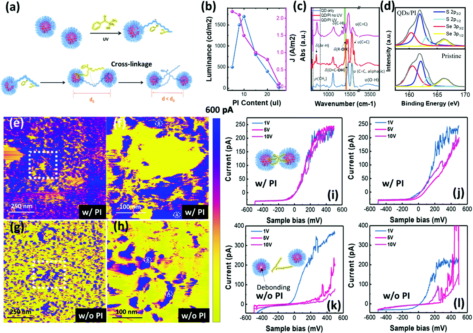 | ||
| Fig. 4 Investigation of degradation mechanism. (a) Schematic illustration of photoinitiated cross-linking reaction. (b) Luminance and current density with respect to the PI content in the QD solution. (c) FT-IR spectra (under vacuum) of QDs and QD/PI before and after UV treatment. (d) XPS spectra of QDs and cross-linked QD/PI with UV treatment after applying external current for 10 min (e–h) Current mapping for the QD/PI layer (e and f) and the QD layer (g and h). (i and j) I–V profile of the QD/PI layer for A region (i) and B region (j). (k and l) I–V profile of the pristine QD layer for A region (k) and B region (l). Inset shows a schematic illustration of QD films at high voltage. | ||
Moreover, excess PI accelerated self-polymerization or continuous polymerization with oleic acid, generating large insulating polymers. This accounted for 20 μL of PI, which rapidly decreased the current density of the QLED devices. The low luminance of the QLED devices with low PI concentration (below 10 μL) was because of inhomogeneous film formation owing to unstable droplets. The FT-IR spectra identified the crosslinking between ligands of QDs benefitted from the PI activated by UV (Fig. 4c). The QD film without any PIs exhibited dominant peaks for aliphatic C![[double bond, length as m-dash]](https://www.rsc.org/images/entities/char_e001.gif) C stretching and O–H stretching and O–H bending (1430 cm−1) owing to oleic acid, whereas peaks at 720 and 1415 cm−1 appeared for QDs with a PI before UV exposure and corresponded to aromatic C–H out-of-plane bending and alcohol O–H bending in PIs, respectively. After UV treatment, the peak related to aliphatic CC stretching diminished and another peak at 1380 cm−1 appeared, which is evidence to verify the crosslinking between ligands (oleic acid) of QDS. The TEM image in Fig. S14 (ESI†) also showed that the intermolecular distance between QDs decreased after UV treatment owing to a cross-linking reaction.
C stretching and O–H stretching and O–H bending (1430 cm−1) owing to oleic acid, whereas peaks at 720 and 1415 cm−1 appeared for QDs with a PI before UV exposure and corresponded to aromatic C–H out-of-plane bending and alcohol O–H bending in PIs, respectively. After UV treatment, the peak related to aliphatic CC stretching diminished and another peak at 1380 cm−1 appeared, which is evidence to verify the crosslinking between ligands (oleic acid) of QDS. The TEM image in Fig. S14 (ESI†) also showed that the intermolecular distance between QDs decreased after UV treatment owing to a cross-linking reaction.
Owing to the cross-linking reaction, the closely packed QD layer exhibited better environmental stability. We performed conductive-AFM (c-AFM) and X-ray photoelectron spectroscopy (XPS) to investigate the environmental stability after a cross-linking reaction. When the external current (100 mA cm−2) was applied for 10 min under ambient conditions, InP QDs underwent different behaviors with and without a PI. The doublet S 2p and Se 3p in S 2p XPS spectra of pristine InP QDs were observed because of the gradient shell structure.52–54 After applying external current, the peaks for Se 3p are relatively increased, whereas cross-linked InP QD/PI exhibited no significant change (similar to pristine QDs before applying external current) (Fig. 4d), which could lead to the enhanced stability of QDs with PI, e.g. lifetime of QLEDs.55
In addition, the c-AFM in the air helped to analyze the electrical behavior of the QD film on the atomic scale. For c-AFM, a 20 nm Au film was first deposited on the Si substrate. The edge of the Si and the bottom that was connected to the chuck for the sample bias was connected by the Ag paste. The QDs and QDs with a PI (both approximately 20 nm thick) were printed directly next to each other on the same Au/Si substrate to minimize any influence of other experimental and environmental factors (Fig. S15a, ESI†). Both layers were exposed to UV for 5 min; then, the boundary region was scanned to investigate the electrical properties on the edge of the QD films. We varied the potential through a tip bias rather than a sample bias to improve the spatial resolution for c-AFM because the sample bias would spread the current through all areas of the sample. A tip bias of 1 V with a 1 V sample bias was applied for current mapping measurements (Fig. 4e–h). Height profiles at the QD island (a 1 μm × 1 μm scan size) demonstrated 3.05 nm in RMS roughness for the QD film with a PI and 2.39 nm in RMS roughness for the film without a PI (Fig. S15b–f, ESI†). Interestingly, the two films had different conductivity distributions despite their similar heights in the scanning region. Tunneling current mapping for the same region found similar mean current levels of around 1.13 nA for the QD/PI and 1.14 nA for the pristine QD (the region below 10 pA was excluded to calculate the mean current level), although the current distribution of each film was different (Fig. S16a and b, ESI†). The pristine QD film had an area showing above 1 nA (1166 nm2), which was approximately one-tenth of that of the film with a PI (10497 nm2). Cross-linking between the QDs appeared to improve the homogeneity of the current distribution in the film with a PI.
We also used c-AFM to investigate the high-voltage degradation of the QDs. Through the c-AFM, a potential window was applied through the tip bias to induce QLED degradation, which is normally observed by a rapid current drop. Current–voltage spectra at two different areas where the current was densest were chosen to analyze the current behavior on the edge of an unstable region owing to a high number of voids between the QDs. The atomic-scale I–V characteristics under ambient conditions showed a slightly lower current level for the QDs with a PI (∼240 pA at 1 V tip bias, 500 mV sample bias) than for the pristine QDs (∼370 pA at 1 V tip bias, 500 mV sample bias) despite the similar height profiles of both films (Fig. 4i–l). This means that the film with a PI had a denser interface than that without a PI. The operational stability of each film was then assessed by measuring the local conductivity changes with increasing tip bias. No significant change in the current depending on the tip bias should appear because of the much greater area for the sample bias compared with the tip bias. A high tip bias was only applied to induce a local high voltage to facilitate QD degradation. Differing I–V characteristics appeared with and without a PI at different external biases (tip bias: 1, 5, and 10 V; sample bias: −600 to 600 mV).
The tunnelling current characteristics of the film with a PI at both locations showed no significant difference at 5 and 10 V of a tip bias (Fig. 4i and j), whereas a dramatic current drop above 5 V occurred for the pristine QD film (Fig. 4k and l). The tunnelling current between the sample and tip is related to the sum of the resistance of the bare substrate, tunnelling through the air, and material resistance. The current changes were predominantly affected by the resistance of the material because we used the PeakForce TUNA mode (the peak force tapping mode c-AFM within the same sample with the same sample-to-tip distance). The major drop in the resistance of the pristine QD film was attributed to hopping between the QDs, which was related to the interfacial electron transfer through the ligand shell.56 In other words, ligand dissociation occurred at high voltage for pristine QD films, a well-known cause of QLED degradation.57,58 This hinders electron transfer between the QDs and further facilitates oxidative degradation of the QDs, leading to a rapid current drop on the atomic and microscale.31,59,60 This result is also associated with the previous XPS results shown in Fig. 4d. Therefore, a thinner QD film without a PI demonstrated absolute current degradation in an inhomogeneous area (Fig. S15c, ESI†). However, cross-linked QDs prevented debonding between the QDs at high voltages and maintained carrier transport between the layers.
We fabricated hole-only devices (ITO/PEDOT:PSS/PVK:TFB/QD/MoO3/Ag in Fig. S17, ESI†) to observe the carrier transport behavior with and without a PI. The mobility of the cross-linked QDs/PI was slightly higher than that of the pristine QDs. Interestingly, we observed significant differences through the reverse-bias analysis. The cross-linked QDs demonstrated a 10 nA current with reverse bias under the high-voltage region. Conversely, the pristine QDs exhibited a high current flow with reverse bias. The current level in the high-voltage region was even higher than that obtained by the forward bias. In addition, the cross-linked QDs/PI showed no significant changes when applying the second round of forward bias, whereas the leakage current of the pristine QDs increased from 10−7 A to 10−6 A owing to debonding between QDs. This means that cross-linking QDs with a PI facilitated electron-blocking behavior toward the HTL, which prevented operational degradation.
In addition to green QDs, we inkjet-printed red and blue QDs on PEN on a large scale (3.4 in). The blue QDs exhibited similar conditions for the best line resolution to green QDs (25 μm drop spacing with 15 mg mL−1), whereas the red QDs showed the best line resolution at a 25 μm drop spacing of 12 mg mL−1 owing to the larger particle size. We printed letters, numbers, and lines using the different QDs, and they all showed strong PL emissions, as shown in Fig. 5a. Moreover, all three QDs were printed together within one symbol to show an excellent line resolution. The different QDs were also printed separately to estimate the EL performance of each QD (device structure: ITO/PEDOT:PSS/PVK:TFB/QD/ZnMgO/Al). The EL spectra of the red, green, and blue QDs demonstrated clear peaks at 455 nm (61 nm FWHM), 550 nm (45 nm FWHM), and 659 nm (55 nm FWHM), respectively, which were similar to the PL spectra of the original materials (Fig. 5b). Fig. 5b–d shows the current density and luminance of the red and blue inkjet-printed QLEDs. The red QLEDs turned on at approximately 11 V, and the luminance consistently increased with increasing operating voltage, reaching 2500 cd m−2 at 13 V. The blue device turned on at approximately 8 V, and the luminance consistently increased with increasing operating voltage, reaching 400 cd m−2 at 14 V. The lower performance of the blue QLEDs was owing to the lower PLQY of the blue InP/ZnSe1−xSx QDs. An RGB EL device with a bird-shaped pattern on glass and flexible substrate (Fig. 5e and f) was fabricated without any supporting structure. The great controllability of the thickness and line resolution of each of the QDs allowed three different colors to be applied along a curved shape in one passive-type EL device; the flexible device remained functioning until a tensile strain of ε = 40%. Finally, a flexible QLED was also successfully fabricated on PEDOT:PSS/PEN owing to the good mechanical strength of the QD layer after cross-linkage. EL devices with an RGB line pattern (Fig. 5b, inset), a 200 μm × 100 μm green QD dot, and white lettering were fabricated using a flexible anode (PEDOT:PSS/PVK:TFB/QD/ZnMgO/Al; Fig. S18, ESI†). The SEM image demonstrated no significant damage to the QLED heterostructure at a tensile strain of ε = 60%, whereas the QLED without a PI indicated many cracks at this strain (Fig. S19, ESI†). This is the first demonstration of a working RGB printed EL device with a specific pattern made without any lithography method, including a bank structure (Table S1, ESI†).
 | ||
| Fig. 5 Three color patterned PL and EL. (a) PL image with red, green, and blue QDs/PI. (b) EL spectra for red, green, and blue QLEDs; inset shows PL and EL images of the printed QLEDs. (c and d) J–V–L characteristics of printed red (c) and blue QLEDs (d) (e and f) Photography of bird-shaped red, green, blue mixed QLEDs on glass (e) and PEN (f). | ||
6. Conclusions
In conclusion, we developed a new method to produce a high-quality printed QD film. A low boiling point solvent was used as the main solvent to minimize the coffee ring effect attributed to the dissolution of the HTL (e.g., TFB or PVK). Issues related to clogging and the viscosity of the ink were resolved through PIs. The low molecular weight of the PI did not disrupt carrier transfer between the QDs, rather it improved due to the UV-induced cross-linking reaction. As a result, better coating (i.e., low surface roughness, thickness control, and packing density) was obtained for the PI mixed QD ink, leading to a high maximum luminescence on printed EL devices. Red, green, and blue mixed QLEDs were successfully fabricated in various patterns on glass and PEN substrates. This work will be extended to any color QLEDs via mixing different emissive QD materials in the future.Author contributions
H. L. and J. M. K. conceived the project. H. L. conducted experiments on the fabrication of devices and characterisations, collected and interpreted the data, and wrote the draft of the manuscript. Y. S conducted the experiments on materials synthesis. X. F., L. N., J. Y., Y. K., J. J., H. W. C., and S. J. interpreted the data. D. S. and S. L. guided the project and revised the manuscript. J. M. K supported all research activities and revised the manuscript.Conflicts of interest
There are no conflicts to declare.Acknowledgements
This work was supported by the European Commission (H2020, 1D-NEON, Grant agreement ID:685758) and the UK Research and Innovation (EPSRC, EP/P027628/1).References
- Y. Shirasaki, G. J. Supran, M. G. Bawendi and V. Bulović, Nat. Photonics, 2013, 7, 13–23 CrossRef CAS.
- M. K. Choi, J. Yang, T. Hyeon and D.-H. Kim, npj Flexible Electron., 2018, 2, 1–14 CrossRef.
- H. Shen, Q. Gao, Y. Zhang, Y. Lin, Q. Lin, Z. Li, L. Chen, Z. Zeng, X. Li and Y. Jia, Nat. Photonics, 2019, 13, 192–197 CrossRef CAS.
- D. Kim, Y. Fu, S. Kim, W. Lee, K.-H. Lee, H. K. Chung, H.-J. Lee, H. Yang and H. Chae, ACS Nano, 2017, 11, 1982–1990 CrossRef CAS PubMed.
- H. Zhang, S. Chen and X. W. Sun, ACS Nano, 2018, 12, 697–704 CrossRef CAS PubMed.
- U. Resch-Genger, M. Grabolle, S. Cavaliere-Jaricot, R. Nitschke and T. Nann, Nat. Methods, 2008, 5, 763–775 CrossRef CAS PubMed.
- L. Zhou, X. Chen, W. Su, Z. Cui and W. Y. Lai, Adv. Mater. Interfaces, 2022, 2102548 CrossRef CAS.
- L. Zhou, L. Yang, M. Yu, Y. Jiang, C.-F. Liu, W.-Y. Lai and W. Huang, ACS Appl. Mater. Interfaces, 2017, 9, 40533–40540 CrossRef CAS PubMed.
- L. Zhou, M. Yu, X. Chen, S. Nie, W. Y. Lai, W. Su, Z. Cui and W. Huang, Adv. Funct. Mater., 2018, 28, 1705955 CrossRef.
- L. Zhou, M. Yu, L. Yao and W.-Y. Lai, Adv. Eng. Mater., 2022, 2101558 CrossRef.
- J. Han, D. Ko, M. Park, J. Roh, H. Jung, Y. Lee, Y. Kwon, J. Sohn, W. K. Bae and B. D. Chin, J. Soc. Inf. Disp., 2016, 24, 545–551 CrossRef CAS.
- R. S. Deol, H. W. Choi, M. Singh and G. E. Jabbour, IEEE Sens. J., 2014, 15, 3186–3195 Search PubMed.
- V. Wood and V. Bulović, Nano Rev., 2010, 1, 5202 CrossRef PubMed.
- J. Kettle, T. Lamminmäki and P. Gane, Surf. Coat. Technol., 2010, 204, 2103–2109 CrossRef CAS.
- H. Minemawari, T. Yamada, H. Matsui, J. Y. Tsutsumi, S. Haas, R. Chiba, R. Kumai and T. Hasegawa, Nature, 2011, 475, 364–367 CrossRef CAS PubMed.
- E. Fisslthaler, S. Sax, U. Scherf, G. Mauthner, E. Moderegger, K. Landfester and E. J. List, Appl. Phys. Lett., 2008, 92, 165 CrossRef.
- D. Kim, Y. Jeong, K. Song, S.-K. Park, G. Cao and J. Moon, Langmuir, 2009, 25, 11149–11154 CrossRef CAS PubMed.
- C. N. Hoth, S. A. Choulis, P. Schilinsky and C. J. Brabec, Adv. Mater., 2007, 19, 3973–3978 CrossRef CAS.
- H. M. Haverinen, R. A. Myllyla and G. E. Jabbour, J. Disp. Technol., 2010, 6, 87–89 CAS.
- C. Jiang, H. W. Choi, X. Cheng, H. Ma, D. Hasko and A. Nathan, Science, 2019, 363, 719–723 CrossRef CAS PubMed.
- N. Adly, B. Bachmann, K. Krause, A. Offenhäusser, B. Wolfrum and A. Yakushenko, RSC Adv., 2017, 7, 5473–5479 RSC.
- B. Huber, P. Popp, M. Kaiser, A. Ruediger and C. Schindler, Appl. Phys. Lett., 2017, 110, 143503 CrossRef.
- Y. Liu, F. Han, F. Li, Y. Zhao, M. Chen, Z. Xu, X. Zheng, H. Hu, J. Yao and T. Guo, Nat. Commun., 2019, 10, 1–9 CrossRef PubMed.
- S. Keuleyan, E. Lhuillier, V. Brajuskovic and P. Guyot-Sionnest, Nat. Photonics, 2011, 5, 489–493 CrossRef CAS.
- R. Weissleder, Nat. Biotechnol., 2001, 19, 316–317 CrossRef CAS PubMed.
- C.-T. Wang and S.-C. Yen, Chem. Eng. Sci., 1995, 50, 989–999 CrossRef CAS.
- Y. Liu, F. Li, Z. Xu, C. Zheng, T. Guo, X. Xie, L. Qian, D. Fu and X. Yan, ACS Appl. Mater. Interfaces, 2017, 9, 25506–25512 CrossRef CAS PubMed.
- A. Katsumiti, D. Gilliland, I. Arostegui and M. Cajaraville, Aquat. Toxicol., 2014, 153, 39–52 CrossRef CAS PubMed.
- V. Wood, M. J. Panzer, J. Chen, M. S. Bradley, J. E. Halpert, M. G. Bawendi and V. Bulović, Adv. Mater., 2009, 21, 2151–2155 CrossRef CAS.
- Y.-H. Won, O. Cho, T. Kim, D.-Y. Chung, T. Kim, H. Chung, H. Jang, J. Lee, D. Kim and E. Jang, Nature, 2019, 575, 634–638 CrossRef CAS PubMed.
- R. P. Brown, M. J. Gallagher, D. H. Fairbrother and Z. Rosenzweig, Langmuir, 2018, 34, 13924–13934 CrossRef CAS PubMed.
- K. D. Wegner, F. Dussert, D. Truffier-Boutry, A. Benayad, D. Beal, L. Mattera, W. L. Ling, M. Carrière and P. Reiss, Front. Chem., 2019, 7, 466 CrossRef CAS PubMed.
- S. Chen, W. Cao, T. Liu, S.-W. Tsang, Y. Yang, X. Yan and L. Qian, Nat. Commun., 2019, 10, 1–9 CrossRef PubMed.
- F. Withers, H. Yang, L. Britnell, A. Rooney, E. Lewis, A. Felten, C. Woods, V. Sanchez Romaguera, T. Georgiou and A. Eckmann, Nano Lett., 2014, 14, 3987–3992 CrossRef CAS PubMed.
- J. Perelaer, P. J. Smith, D. Mager, D. Soltman, S. K. Volkman, V. Subramanian, J. G. Korvink and U. S. Schubert, J. Mater. Chem., 2010, 20, 8446–8453 RSC.
- P. Yang, L. Zhang, D. J. Kang, R. Strahl and T. Kraus, Adv. Opt. Mater., 2020, 8, 1901429 CrossRef CAS.
- J. Kwon, S. Kim, J. Lee, C. Park, O. Kim, B. Xu, B. Kang, J. Bae and S. Kang, Org. Electron., 2019, 74, 166–171 CrossRef CAS.
- T. Xuan, J. Huang, H. Liu, S. Lou, L. Cao, W. Gan, R.-S. Liu and J. Wang, Chem. Mater., 2019, 31, 1042–1047 CrossRef CAS.
- T. Watanabe, Y. Iso, T. Isobe and H. Sasaki, RSC Adv., 2018, 8, 25526–25533 RSC.
- R. D. Deegan, O. Bakajin, T. F. Dupont, G. Huber, S. R. Nagel and T. A. Witten, Nature, 1997, 389, 827–829 CrossRef CAS.
- J. Widmann and E. Davis, Aerosol Sci. Technol., 1997, 27, 243–254 CrossRef CAS.
- D. P. Birnie III, Langmuir, 2013, 29, 9072–9078 CrossRef PubMed.
- X. Shen, C.-M. Ho and T.-S. Wong, J. Phys. Chem. B, 2010, 114, 5269–5274 CrossRef CAS PubMed.
- G. D. Martin, S. D. Hoath and I. M. Hutchings, Rev. Sci. Instrum., 2008, 79, 075108 CrossRef PubMed.
- Y. Son, C. Kim, D. H. Yang and D. J. Ahn, Langmuir, 2008, 24, 2900–2907 CrossRef CAS PubMed.
- L. Wang, J. Pan, J. Qian, W. Lei, Y. Wu, W. Zhang, D. K. Goto and J. Chen, J. Mater. Chem. C, 2018, 6, 8099–8104 RSC.
- N. S. Allen, J. Photochem. Photobiol., A, 1996, 100, 101–107 CrossRef CAS.
- W. K. Bae, Y.-S. Park, J. Lim, D. Lee, L. A. Padilha, H. McDaniel, I. Robel, C. Lee, J. M. Pietryga and V. I. Klimov, Nat. Commun., 2013, 4, 1–8 Search PubMed.
- L. Qian, Y. Zheng, J. Xue and P. H. Holloway, Nat. Photonics, 2011, 5, 543–548 CrossRef CAS.
- V. Kichigin, I. Petukhov, S. Mushinskii, V. Karmanov and D. Shevtsov, Russ. J. Appl. Chem., 2011, 84, 2060–2064 CrossRef CAS.
- P. E. Ludwig and A. Ossenbach, UV+ EB Tech, 2016, 4 Search PubMed.
- K. D. Wegner, F. Dussert, D. Truffier-Boutry, A. Benayad, D. Beal, L. Mattera, W. L. Ling, M. Carrière and P. Reiss, Front. Chem., 2019, 466 CrossRef CAS PubMed.
- H. Rupp and U. Weser, Bioinorg. Chem., 1975, 5, 21–32 CrossRef CAS PubMed.
- H. Virieux, M. Le Troedec, A. Cros-Gagneux, W.-S. Ojo, F. Delpech, C. Nayral, H. Martinez and B. Chaudret, J. Am. Chem. Soc., 2012, 134, 19701–19708 CrossRef CAS PubMed.
- P. Ramasamy, B. Kim, M.-S. Lee and J.-S. Lee, Nanoscale, 2016, 8, 17159–17168 RSC.
- R. D. Harris, S. Bettis Homan, M. Kodaimati, C. He, A. B. Nepomnyashchii, N. K. Swenson, S. Lian, R. Calzada and E. A. Weiss, Chem. Rev., 2016, 116, 12865–12919 CrossRef CAS PubMed.
- H. Moon, C. Lee, W. Lee, J. Kim and H. Chae, Adv. Mater., 2019, 31, 1804294 CrossRef PubMed.
- J. Lim, Y.-S. Park, K. Wu, H. J. Yun and V. I. Klimov, Nano Lett., 2018, 18, 6645–6653 CrossRef CAS PubMed.
- C. Xiang, L. Wu, Z. Lu, M. Li, Y. Wen, Y. Yang, W. Liu, T. Zhang, W. Cao and S.-W. Tsang, Nat. Commun., 2020, 11, 1–9 CrossRef PubMed.
- C. Pu, X. Dai, Y. Shu, M. Zhu, Y. Deng, Y. Jin and X. Peng, Nat. Commun., 2020, 11, 1–10 CrossRef PubMed.
Footnote |
| † Electronic supplementary information (ESI) available. See DOI: https://doi.org/10.1039/d2tc00851c |
| This journal is © The Royal Society of Chemistry 2022 |