DOI:
10.1039/D2TC00759B
(Paper)
J. Mater. Chem. C, 2022,
10, 11027-11039
Controlled growth of 3D assemblies of edge enriched multilayer MoS2 nanosheets for dually selective NH3 and NO2 gas sensors†
Received
23rd February 2022
, Accepted 30th June 2022
First published on 22nd July 2022
Abstract
Herein, we report on the successful controlled growth of edge enriched 3D assemblies of MoS2 nanosheets by adjusting the gas flow rate during atmospheric pressure CVD. The results revealed that 30 ml min−1 was the optimal flow rate, in which the growth direction shifts from in-plane nanosheets to out-of-plane 3D assemblies of MoS2 nanosheets. It is suggested that, at this flow rate, we have an ideal tradeoff between the surface interaction and the mass transport of precursor molecules. Morphological, structural and chemical composition analyses showed the formation of vertically oriented MoS2 nanosheets with MoO3−x impurities, resulting from the incomplete sulfurization during the synthesis. Based on the morphological evolution of the studied material, the growth mechanism was explored. The gas sensing properties of the as grown films were tested against NH3 and NO2. They exhibited stable and reproducible responses with excellent sensitivity to ppm-level NH3 (20% response to 2 ppm) and ppb-level NO2 (11% response to 20 ppb). Additionally, this nanomaterial showed dual selectivity towards NH3 at room temperature and NO2 at 100 °C. To the best of our knowledge, none of the reported studies on MoS2 based gas sensors have described this dual selectivity. The experimental detection limit was below 2 ppm for NH3 while it was below 20 ppb for NO2. Besides, the vertical growth of edge enriched MoS2 bestows the sensors with notable resilience against high levels of ambient humidity. The sensor response was only slightly increased (R = 70%) in a humid environment compared to a dry background (R = 65%) when measuring 800 ppb of NO2. Therefore, this paper shows for the first time that by adjusting the flow rate it is possible to tune the morphology of AP-CVD grown MoS2 for achieving a 3D sponge-like assembly of nanoflakes, showing high sensitivity to NO2 and NH3 and low humidity cross-sensitivity. In addition, the nanomaterial can be made quite specific for detecting NO2 or NH3 by selecting its operating temperature.
Introduction
Graphene with its hexagonal lattice structure was the first two dimensional (2D) material that fascinated researchers and scientists, thanks to its unique properties and broad relevant applications.1–3 In contrast to conventional gas sensors based on MOX nanostructures,4,5 graphene offers some advantages such as large specific surface area (i.e., atomically 2D form), high conductivity, moderate operating temperatures, and low electrical noise.6,7 However, its lack of band gap prevents this material from exhibiting semiconducting properties.4,8 This shortcoming is relevant for developing chemoresistive gas sensors and has inspired researchers to move towards other atomically layered 2D semiconductor materials with a defined band gap. Among the 2D materials that have been identified and investigated for gas sensing applications, we found tin sulfide (SnS2), molybdenum selenide (MoSe2), tungsten disulfide (WS2), molybdenum disulfide (MoS2), phosphorene and tellurene only to cite a few.9–16
Molybdenum disulfide belongs to the family of transition metal dichalcogenide (TMD) materials, in which molecular layers are stacked together by van der Waals forces. It is an n-type semiconductor with a band gap ranging from 1.2 eV for the bulk MoS2 (indirect band gap) to 1.83 eV for the monolayer MoS2 (direct and wider band gap).17 Indeed, the bandgap of TMD materials depends on the number of their atomic layers, which provides different possibilities for their application in various fields such as optoelectronics,18 solar cells,19 photocatalysis and gas sensors.20 It was reported that a high quality monolayer fit well with FET devices, whereas few layer TMDs are suitable for gas sensing applications. Babar and co-workers found that bilayer and hetero-bilayer MoS2 and WS2 showed improved gas sensing performances compared to their monolayers.21 Late and co-workers showed that few layer MoS2 exhibited excellent sensing performances towards NO2, NH3 and humidity, compared to the MoS2 single layer.22 Additionally, obtaining a continuous monolayer is very challenging, and most reports describe the synthesis of discontinue monolayer domains dispersed on the top of the substrate.23–25 This non-continuity is a drawback for their use in chemoresistive transduction schemes in gas sensing applications.
Recently, the three-dimensional (3D) assembly of multilayer TMD nanosheets has attracted the attention of many researchers, since the gas adsorption at the edge sites of the TMD nanosheets is more significant than at their basal plane, thus enhancing sensitivity and selectivity.26–28 In the case of MoS2, its basal plane is most of the times used as a chemical receptor, because it is easy to expose and produce using exfoliation or chemical vapor deposition techniques. However, this basal plane surface has minimal dangling bonds, and due to thermodynamic forces, it is difficult to expose their edge sites to the environment.29,30 In contrast, in 3D MoS2 nanosheets, the edge sites have a local stoichiometry with physical and electronic properties that make them more exposed. Moreover, the vertical nanosheets are formed by the (002) plane, which usually ends with the predominance of either exposed molybdenum atoms or exposed sulfur atoms.31,32 Cho and coworkers reported highly enhanced gas adsorption properties in vertically aligned MoS2 layers.29 They found about 5-fold enhanced sensitivity to NO2 gas molecules compared to horizontally aligned MoS2 films. This finding was corroborated by density functional theory (DFT) calculations. Lee and co-workers showed that the addition of active edge sites enhances the surface-to-mass ratio and the resulting gas-sensing properties.26 Agrawal and co-workers reported that the total surface free energy of MoS2 increases by increasing the density of the edge sites, which enhances the catalytic activity of the MoS2 material.27 Therefore, it is essential to develop 3D assemblies of edge enriched MoS2 networks rather than in-plane MoS2 lattice geometries for the fabrication of highly sensitive gas sensors. The most reported techniques that are used for this growth are hydrothermal and atmospheric pressure CVD (APCVD).33–37 Using the hydrothermal method to synthesize MoS2 nanosheets, hazardous precursors such as molybdenum chloride are needed, which can release harmful chloride vapors. Moreover, it involves a many-step fabrication process and, thus, it is a time-consuming technique. Conversely, in the APCVD technique, we need sulfur and molybdenum precursor sources. The deposition occurs in a single step, at atmospheric pressure without the assistance of hydrogen, in a self-catalyzed process. It has a large yield with a direct deposition onto the sensor substrate. Additionally, it is a catalyst free technique.
In the literature, there are few reports on 3D assemblies of edge enriched MoS2 nanosheets for gas sensing applications. For instance, Agrawal and co-workers presented photoactivated mixed in-plane and edge-enriched p-type MoS2 flake-based NO2 sensors working at room temperature.34 In that study, the vertical flakes were not interconnected between them, and there were more in-plane flakes rather than edge enriched vertical ones. Moreover, the sensors were assisted by UV light and the NO2 concentrations tested were very high, ranging from 10 to 500 ppm. Jaiswal and co-workers reported vertically aligned edge-oriented MoS2 nanostructured thin films functionalized by Pd nanoparticles for gas sensing applications.38 These films were deposited via a single step dc-magnetron sputtering technique. Their morphology was characterized by a continuous porous film with dispersed grains and the absence of a multilayer MoS2 nanosheet network. Besides, the fabricated sensor showed low sensitivity against very high concentrations of NH3 and NO2 gases, at room temperature. The responses were 2.5% and 5% against 500 ppm of NH3 and NO2, respectively. Hang and coworkers studied the controlled growth of vertically oriented three-layer MoS2 nanoflakes for room-temperature NO2 gas sensor applications.39 The density and thickness of MoS2 nanosheets were controlled by varying the heating rate of a CVD process conducted under vacuum. The fabricated sensors displayed good sensitivity and selectivity towards NO2. The response towards 0.5 ppm NO2 at room temperature was 20.1%. However, the effect of ambient humidity cross-sensitivity was not studied.
In this paper, we report for the first time the successful controlled growth of, large scale, 3D assemblies of edge enriched MoS2 nanosheets using a single step atmospheric pressure CVD method for the fabrication of dually selective NH3 and NO2 gas sensors. During depositions, no hydrogen assistance was used. The films were obtained by controlling the argon gas flow rate during the APCVD process. In addition, they were directly grown on the sensor substrate without the need for further fabrication steps or seeding with noble metals. Moreover, an extensive material characterization study of the as grown nanostructured films was performed by using FE-SEM to analyze the morphology, XRD and Raman spectroscopy to verify the structure, and XPS and HRTEM to identify the chemical composition. Besides this, the growth mechanism was thoroughly studied by analyzing the morphology evolution of the 3D assembly of MoS2 nanosheets, which is not often reported in the literature. The gas sensing performance of the synthesized films was tested against low concentrations of NH3 and NO2 (at concentrations under the threshold limits defined for health safety standards). Sensors were operated at room temperature and at 100 °C and tested under dry and humid (50% R.H.) conditions. Sensors showed high sensitivity with dual selectivity behavior. Namely, they were selective to NH3 when operated at room temperature and NO2 when operated at 100 °C. It is worth noting that reports on MoS2 based gas sensors have never reported such advantageous dual selectivity towards two different pollutant gases.
Experimental section
Material synthesis
The atmospheric pressure CVD (APCVD) method was employed to grow the edge enriched 3D assemblies of MoS2 nanosheets. As it is shown in Fig. S1a (ESI†), the system was composed of a quartz tube-in-tube growth chamber, a heating belt and a CVD furnace. The small quartz tube has a diameter of 15 mm while the large tube is 38 mm in diameter. Before starting the synthesis, the substrate (SiO2, 300 nm) was cleaned with acetone (30 min), isopropanol (30 min) and distilled water. Then, it was dried in air, placed vertically in a homemade ceramic support and then pushed inside the CVD furnace. MoO3 powder (25 mg, 99.97%, Sigma-Aldrich) and sulfur powder (700 mg, 99.97%, Sigma-Aldrich) were loaded separately in two ceramic boats and located in distinct zones (heating belt and CVD furnace) in order to provide independent temperature control. The distance between MoO3 and S was 25 cm while the distance between MoO3 and the substrate was 5 cm. The APCVD synthesis procedure was composed of five steps: (1) the growth chamber (tube-in-tube) was flushed with argon (500 ml min−1) for 30 min in order to remove oxygen molecules; (2) the furnace was ramped to 850 °C under an Ar flow of 100 ml min−1; (3) once the furnace reached 500 °C, the heating belt (200 °C) was powered on, and the sulfur began to evaporate (Fig. S1b, ESI†); (4) when the temperature of the furnace reached 850 °C, the Ar flow was modified and set according to the different growth conditions (10, 30 or 70 ml min−1) for 60 min; (5) the furnace was left to cool down while the heating belt was kept ON, to provide a sufficiently sulfur rich atmosphere, thus avoiding the oxidation of the film deposited.
Material characterization techniques
The morphology of the prepared samples was analyzed using a scanning electron microscope (SEM-FET quanta 600) coupled with a field-emission scanning electron microscope (FESEM) Hitachi 2000 and FEI Helios Nanolab 650. The crystal structure at the atomic level was studied by high-resolution transmission electron microscopy (HRTEM) (Jeol, JEM-2100) and X-ray diffraction using a Bruker-AXS D8-Discover diffractometer equipped with a parallel incident beam (Gober mirror), vertical XYZ motorized stage and with a GADDS (General Area Diffraction System). Elemental and chemical analyses were performed via X-ray photoelectron spectroscopy (XPS) using a versaprobe PHI5000 spectrometer (equipped with a monochromatic Al Kα X-ray source). For data analysis, the CASA XPS software was used. The Raman spectra were recorded using a Renishaw inVia, laser 514 nm, ion argon-Novatech, 25 mW.
Gas sensing measurements
Gas sensing measurements were performed in a Teflon chamber with a volume of 35 ml. The test chamber has an inlet and an outlet and connectors for housing up to four sensors at the same time. The inlet was connected to the gas delivery system and the outlet was connected to the exhaust. Regarding the sensors, they were fabricated in our lab by connecting two platinum wires to the growth substrate using the silver paste as depicted in Fig. S2 (ESI†). Besides this, the substrate was attached to a ceramic hotplate that comprised a platinum resistive heater, using a conductive epoxy. This allowed increasing the operating temperature above room temperature when needed. Finally, the whole device was wire-bonded to a PCB that could be plugged inside the test chamber. The sensor responses were obtained by monitoring the sensing film resistance using an Agilent-34972A multimeter. To acquire the target concentration, calibrated cylinders of nitrogen dioxide (total concentration, 1 ppm), ammonia (total concentration, 100 ppm), hydrogen (total concentration, 1000 ppm) and carbon monoxide (total concentration, 100 ppm) were mixed with pure synthetic air using Bronkhorst mass-flow controllers and associated software. The total flow rate was kept constant at 100 ml min−1 during all the experiments. The exposure time to the target gas was fixed to 10 min, while the duration of the cleaning phase (dry air) was adapted to the sensor operating temperature. It was 50 min for measurements performed at 100 °C and 120 min for the ones realized at room temperature. For calibrating the sensors, we expose them to dry air for 4 hours before each cycling measurement and for 1 night before measuring a new gas. This calibration was needed in order to reach the initial baseline resistance and clean the sensor surface as well as the chamber. Moreover, humidity measurements were conducted by introducing 50% of relative humidity during the hole gas cycling measurements. The sensor response was calculated by using eqn (1) for reducing species and by eqn (2) for oxidizing ones. Additionally, the response and recovery time are defined as the time required to reach 90% of the total changes in resistance in the case of detection and recovery phases, respectively.| |  | (1) |
| |  | (2) |
Results and discussion
Material characterization
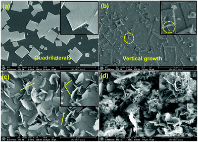
MoS2 nanostructured thin films were synthesized at 850 °C using a tube-in-tube, hydrogen free APCVD method. Samples were directly grown on 300 nm thick SiO2 on Si substrates (1 × 2 cm2) without any further fabrication step. This configuration (tube-in-tube) leads to the stable provision of both gaseous precursors to the reaction area, near the substrate, during the whole deposition. Additionally, it allowed us to avoid the quenching and gradual sulfurization of MoO3 caused by sublimated sulfur. The films were grown under three different carrier gas (Ar) flow rate conditions: 10, 30 and 70 ml min−1 and were labelled as MoS2-10, MoS2-30 and MoS2-70, respectively. Fig. 1 depicts the FE-SEM images obtained from the three samples. It is clear that the flow rate significantly affected the obtained morphologies. At an argon gas flow rate of 10 ml min−1, we achieved sparse multilayer MoS2 nanotriangles dispersed all over the substrate (Fig. 1(a)). Each one consisted of several nanotriangles deposited on top of each other, forming a pyramidal shape. More images are provided in the ESI,† Fig. S3. When the argon gas flow rate was increased to 30 ml min−1, the morphology was changed from in plane MoS2 nanotriangles to out-of-plane, edge enriched 3D assemblies of MoS2 nanosheets (Fig. 1(b)). The film was continuous (Fig. S4, ESI†), completely coating the substrate area. The size of the nanosheets was not completely homogeneous, and they were longer in the center of the substrate while they grew shorter at the borders. A further increase in the argon gas flow rate (70 ml min−1) generated another change in the morphology of the samples. From Fig. 1(c), we can observe a continuous layer of 2D quadrilateral nanostructures with different sizes, deposited randomly over the substrate. Based on the literature, at a low gas flow rate (10 ml min−1), the mass transport of the precursor species limits the amount of the deposited nuclei onto the substrate active sites. In this reaction, the crystal growth is carried out by the thermodynamics regime where the surface chemical reaction rate is proportional to the carrier gas flow rate and the deposited nuclei are grown laterally to form nanotriangles. At a flow rate of 30 ml min−1, the direction growth becomes out-plane and the crystal growth changes from the thermodynamics regime to kinetics one. This case of growth is further studied and illustrated in the growth mechanism section.
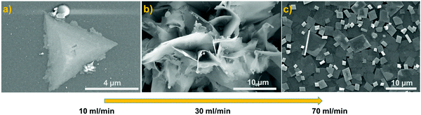 |
| | Fig. 1 FE-SEM images of the grown films using (a) 10 ml min−1 (b) 30 ml min−1 and (c) 70 ml min−1 of argon flow rate. | |
At a high gas flow rate (70 ml min−1), an overdose of the precursors’ species arrived to the substrate active sites, outperforming the rate-ability of the surface reaction that could occur at the deposition temperature (850 °C), leading in gas phase reactions before reaching the substrate sites and depositing nanoflakes at the surface of the substrate. Herein, the CVD is controlled by a surface reaction.40–42
Therefore, at an argon flow rate of 30 ml min−1, we have a perfect fit between the surface interaction and the mass transport of precursor molecules, resulting in a suitable morphology for gas sensor fabrication. In fact, it offers a large surface area to volume ratio with enriched exposed edge sites, has plenty of voids for gas diffusion, and has many defects that make it highly reactive with gas molecules.
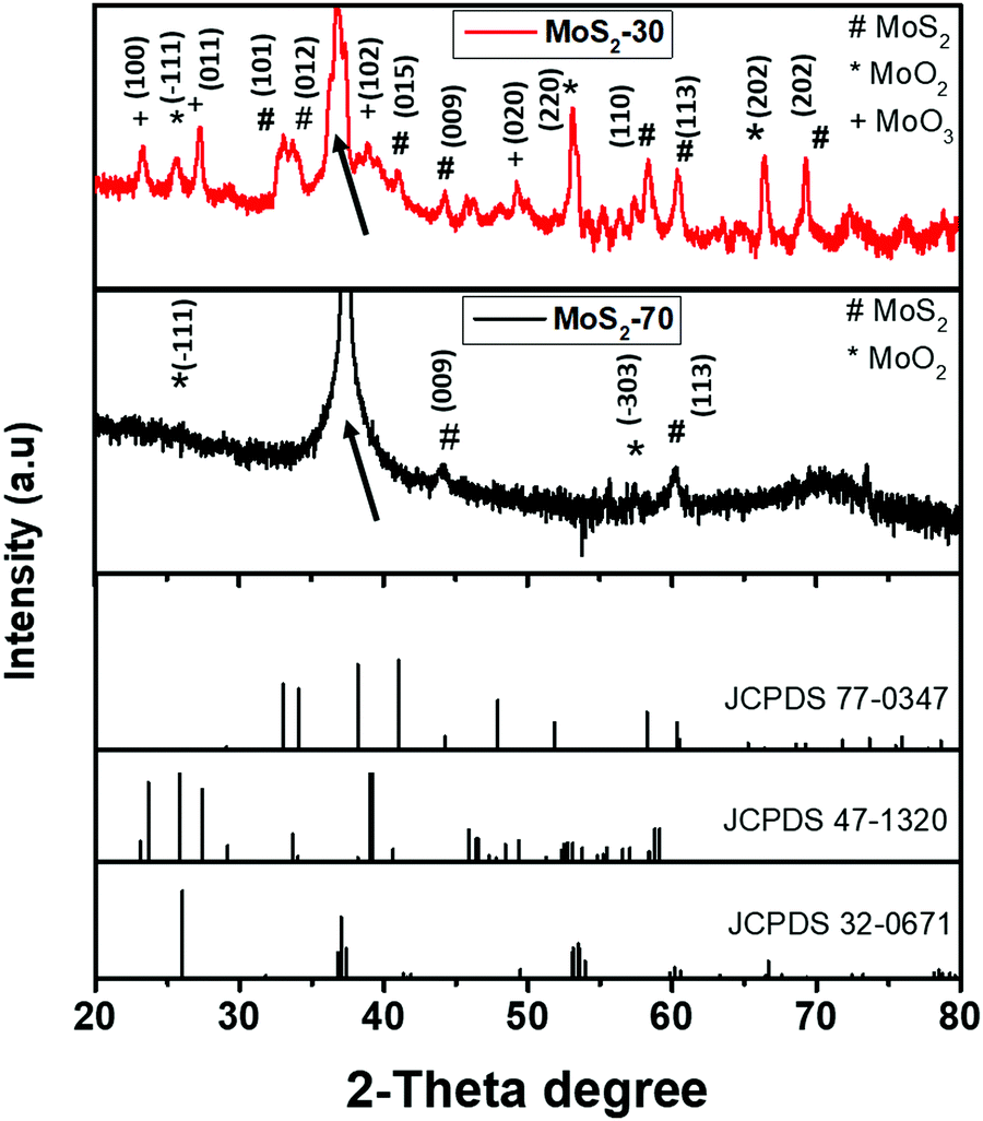
The crystal structure of the films was analyzed by an X-ray diffraction (XRD) method. Fig. 2 shows the XRD patterns recorded for MoS2-30 and MoS2-70 films in the range of 20° to 80°. It can be deduced that the analyzed samples have a polycrystalline structure. For MoS2-30, we detected peaks at 33.4°, 34.1°, 40.9°, 44.2°, 58°, 60° and 69°, which are attributed to the (101), (012), (015), (009), (110), (113) and (202) planes of MoS2, respectively, according to the JCPDS card number (77-0341). Also, we noticed peaks at 25.7°, 36.7°, 37.34°, 53.15° and 66.4°, which belong to the (−111), (200), (−202), (220) and (202) planes of MoO2, respectively, in accordance with the JCPDS card number (32-0671), and peaks located at 23.3°, 27.3°, 38.9° and 49.2° which correspond respectively to the (100), (011), (102) and (020) planes of MoO3 (JCPDS card number: 47-1320). Regarding MoS2-70, we found peaks at 25.9°, 37.4° and 57.4°, indicative of the (−111), (−202) and (−303) planes of MoO2 (JCPDS card number: 32-0671), respectively, and two peaks at 44.2° and 60° assigned to the (009) and (113) planes of MoS2, respectively (JCPDS card number: 77-0341). The peaks indexed by black arrows in Fig. 2 are enlarged and clearly displayed in Fig. S5 (ESI†). It is worth noting that we could not analyze MoS2-10 samples, since the nanotriangles were very small and sparsely dispersed over the substrate; thus it was difficult to localize them. Therefore, the presence of an intermediate MoO3−x in both samples can be associated with the insufficient sulfurization (i.e. the incomplete CVD reaction) of MoO3 and the presence of some oxygen molecules inside the CVD tube during the APCVD. Many studies in the literature reported the presence of these intermediate phases when the MoO3 precursor is used and this is an issue that should be addressed in the future. Based on the literature,43 MoO3 is first reduced to MoO3−x and with further sulfur it is converted to MoS2. Equations (eqn (3) and (4)) describe the conceivable chemical reaction that can occur during the synthesis.
| | | 2MoO3 + xS → 2MoO3−x + xSO2 | (3) |
| | | 2MoO3−x + (7 − x)S → 2MoS2 + (3 − x)SO2 | (4) |
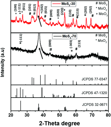 |
| | Fig. 2 XRD patterns recorded for MoS2-30 and MoS2-70 films. | |
Additionally, from the XRD patterns, the MoS2-30 samples contain more MoS2 peaks than those observed in the MoS2-70 samples. This can be related to the CVD reaction time and the amount of sulfur that reaches the substrate. These two parameters are strongly influenced by the gas flow rate used during the deposition.
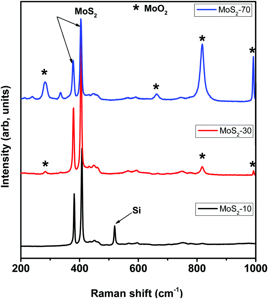
Fig. 3 displays the Raman spectra recorded for MoS2-10, MoS2-30 and MoS2-70 samples. The results showed the presence of two common peaks in all the samples near 400 cm−1. They belong to the two vibration modes of MoS2: the in-plane vibration of molybdenum and sulfur atoms E12g and out-of-plane vibration of sulfur atoms A1g.27,42 Besides, in MoS2-70 samples, we observed other obvious peaks at 283, 336, 663, 818 and 992 cm−1, which are assigned to the MoO2 phase.44–46 Additionally, in MoS2-30, we noticed three of these peaks, located at 283, 818 and 992 cm−1, but with very low intensity. Regarding the MoS2-10 spectrum, we did not detect further peaks rather than the ones of MoS2. Consequently, these Raman results confirm the formation of MoS2 with intermediate MoO3−x products in samples prepared by using 30 ml min−1 and 70 ml min−1, which is in line with the XRD results.
 |
| | Fig. 3 Raman spectra of MoS2-10, MoS2-30 and MoS2-70 films. | |
Table 1 summarizes the position of E12g and A1g MoS2 vibration modes, the difference between them (Δ) and their intensity ratio (Iratio) for all samples. In fact, using Δ information, this helps in inferring the number of MoS2 layers that compose the film. As we can see from Table 1, Δ ≥ 26 indicates the formation of the multilayer MoS2 material in all the grown films. Moreover, the intensity ratio Iratio provides more information about the vertical orientation of the MoS2 nanosheets grown by the APCVD technique. Indeed, the E12g peak resulted from the vibration of the Mo atom in the in-plane and opposite to two S atoms, whereas in the A1g peak the Mo atom is immobile and the two S atoms vibrate in opposite directions in the out-of-plane direction. Hence, E12g is in preference to be emitted from the in plane oriented MoS2 nanosheets, while A1g is preferred by the edge sites of vertically oriented MoS2 nanosheets.42 Therefore, a decrease in the intensity ratio, is correlated with an increase in the vertical orientation of the MoS2 nanosheets. Based on the calculated intensity ratio of all the samples, the lowest ratio was observed for MoS2-30 which exhibits vertically oriented MoS2 nanosheets while the highest one was recorded for the sample composed of 2D nanotriangles. These observations are in line with the FE-SEM results.
Table 1 Summary of Raman data for the as grown samples
| Sample name |
E12g |
A1g |
Δ = (A1g − E12g) |
I
ratio = (E12g/A1g) |
| MoS2-10 |
381 |
408 |
27 |
0.55 |
| MoS2-30 |
379 |
405 |
26 |
0.49 |
| MoS2-70 |
378 |
404 |
26 |
0.52 |
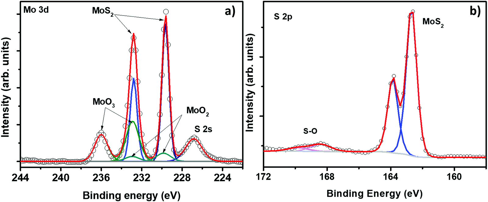
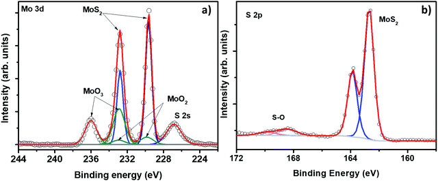
As we have mentioned in the Introduction section, the samples enriched with edge sites are more suitable for gas sensing applications. Consequently, we have further studied the chemical composition and the morphology and the structure of the MoS2-30 films by using XPS and HRTEM analyses. Fig. 4(a) displays the core level spectra of Mo (3d) obtained from the MoS2-30 sample. The molybdenum spectrum exhibits four peaks which were reproduced by three separate doublets. The first one with components, located at 229.5 eV (3d5/2) and 232.8 eV (3d3/2) which correspond to MoS2.27 The second doublet is composed of two small peaks at 229.8 eV (3d5/2) and 232.9 eV (3d3/2), which are attributed to MoO2.27 The last doublet with components at 232.8 eV and 236 eV, which are assigned to MoO3.47 Along with Mo doublets, we have observed a peak at 226.8 which corresponds to S (2s). Fig. 4(b) illustrates the S (2p) spectrum of the MoS2-30 sample. It is composed of an S (2p) doublet positioned at 162.6 eV and 163.8 eV, which correspond to S (2p3/2) and S (2p1/2) spectral lines of S2− in MoS2 and a peak at 168.5 eV. This later can be ascribed to MoOxSy. Thus, the XPS results are in line with the ones obtained from XRD and Raman spectroscopy.47,48
 |
| | Fig. 4 XPS spectra of (a) Mo 3d and (b) S 2p core-levels of the MoS2-30 sample. | |
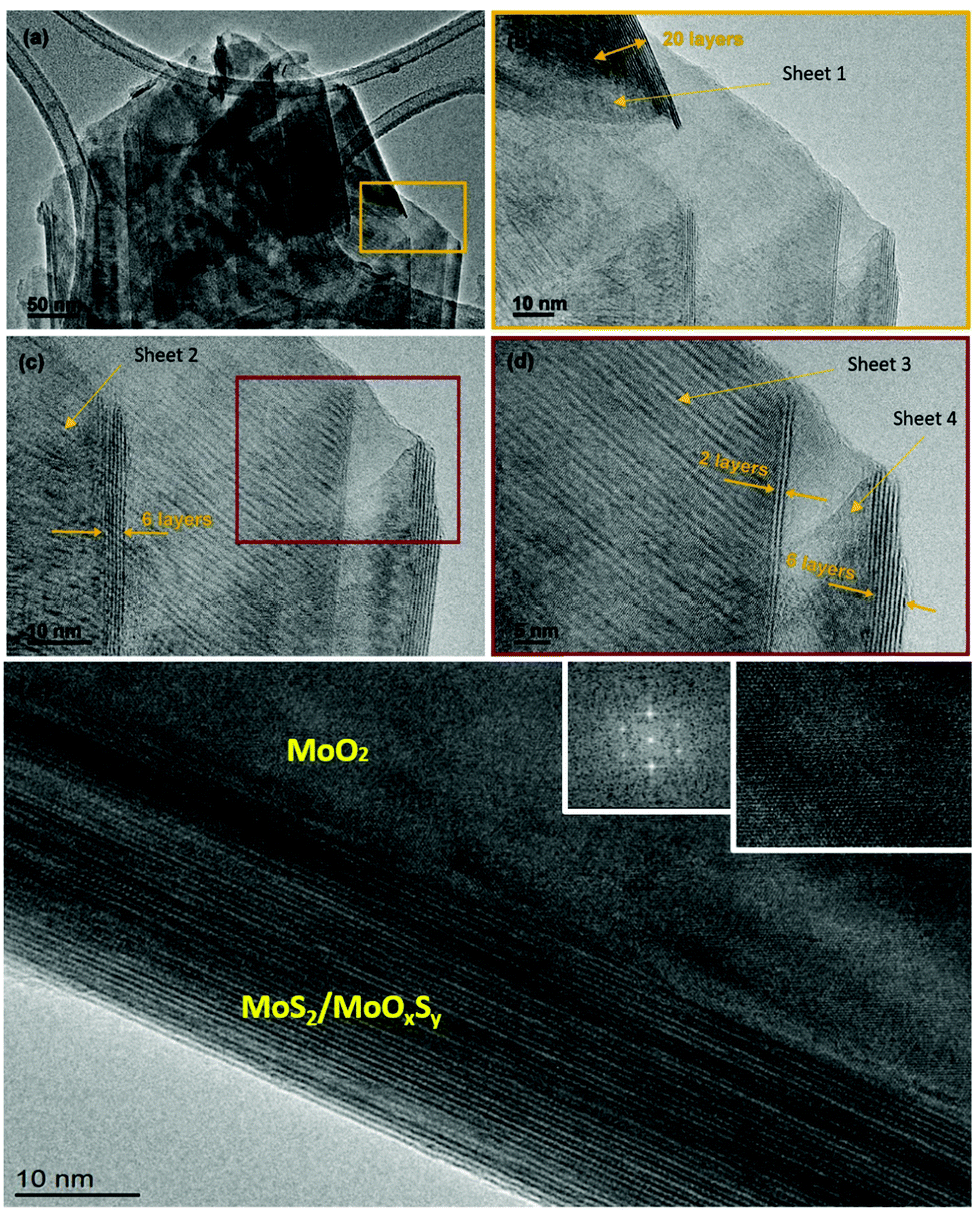
TEM and HRTEM were employed to investigate in detail the morphology and the composition of the MoS2-30 samples. Fig. 5(a) shows multilayer nanosheets with sizes ranging from 400 nm up to 1.5 μm in one dimension. The layers were crystalline, and their surface was very clean without any amorphous material. In addition, in some regions, we detected nanosheets with randomly deposited layers while in other regions the layers were arranged in a stepwise manner. On sheet 1, indexed by an orange arrow in Fig. 5(b), we verified the average interlayer distance measured on 10 fringes, and the calculated value was 0.615 nm, which corresponds to the (002) plane of MoS2 (phase 2H) (JCPDS card number 00-037-1492). In the second sheet (Fig. 5(c)), the measured d-spacing was 0.63 nm (only 6 layers). This distance coincides with the (002) plane of MoS2 (phase 2H) (JCPDS card number 75-1539). In the third sheet (Fig. 5(d)), the d-spacing was 0.27 nm which is assigned to the (100) plane of MoS2.49 In the last sheet (sheet 4, Fig. 5(d)), the d-spacing was 0.68 nm, and it was measured on 6 fringes. This value is ascribed to the expanded interlayer MoS2.50 According to the literature,51 the difference observed in the (002) d-spacing can be explained by the presence of sulfur vacancy defects that produce an expansion at the level of the lattice. In addition to nanosheets, we observed quadrilateral structures (Fig. 5(e)) in which the core level is assigned to the (200) planes of MoO2 (JCPDS card number 32-0671). The d-spacing from the FFT pattern was 0.245 nm. It agrees with the most intense peak observed in the XRD pattern. Regarding the shell of this nanostructure, the measured d-spacing varied between 0.61 nm and 0.56 nm, which indicates the presence of MoS2/MoOxSy. This was observed before in the XPS results and it results from the incomplete sulfurization process of MoO3. In sum, the results obtained from all the material characterization techniques are in good agreement, while HRTEM has clarified and shed light on the morphological composition of MoS2-30 samples. Indeed, it has demonstrated that vertical nanosheets consist of pure MoS2 while the remnant MoO3−x appears in the quadrilateral nanostructures observed. In the next section, more details are given about the morphology and the growth mechanism of this sample.
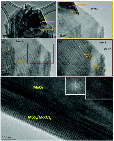 |
| | Fig. 5 HRTEM images of the MoS2-30 sample: (a) TEM images of multilayer MoS2 nanosheets and HRTEM of (b) sheet 1 with a d-spacing of 0.615 nm, (c) sheet 2 with a d-spacing of 0.63 nm, (d) sheet 3 with a d-spacing of 0.27 nm and (e) quadrilateral nanostructures. | |
The APCVD growth mechanism of the edge enriched 3D assemblies of MoS2 nanosheets
Based on the morphological transformation during the growth of the edge enriched MoS2 nanosheets, we have proposed the following growth mechanism, as illustrated in Fig. S6 (ESI†). As a first step, MoO3 vapors get reduced to MoO3−xvia sulfur vapors. This step is well known and is reported by many studies in the literature.52,53 At this level, two different pathway reactions can occur during the deposition:
Reaction (1): the solid phase reaction, in which the intermediate MoO3−x gets adsorbed and diffused onto the substrate forming MoO3−x crystals (mainly MoO2). These later serve as a seeding platform for the growth of MoO3−x particles to eventually create quadrilateral nanostructures (Fig. 6(a)). Next, sulfur vapor will penetrate to the first top layers of MoO3−x quadrilaterals and will change them from MoO3−x to MoS2.27,43,53 This reaction pathway is supported by Fig. 6(e). It should be noted that the XRD, Raman, and XPS techniques used in this work revealed the presence of the intermediate MoO3−x, which could belong to the quadrilateral nanostructures that remain underneath the layer of MoS2 nanosheets. This solid phase reaction can be corroborated by eqn (3) and (4), mentioned above.
 |
| | Fig. 6 Morphological evolution during the growth of edge-enriched 3D assemblies of MoS2 nanosheets. | |
Reaction (2): the vapor-phase reaction, in which the reduced MoO3−x interacts directly with the sulfur at the gas phase and forms the MoS2 vapor. Based on the standard Stranski–Krastanov (SK) growth model,27,53 when the MoS2 vapor diffuses to the substrate and finds one or many MoS2 monolayers, the in-plane growth will be unfavorable and MoS2 will nucleate vertically (Fig. 6(b)) and will change to vertically oriented MoS2 nanosheets, as illustrated in Fig. 6(c) and (d). The suggested vapor-phase reaction can be assisted by eqn (5).
| | | 2MoO3(g) + 7S(g) → 2MoS2(g) + 3SO2(g) | (5) |
Hence, from the FE-SEM results (Fig. 6), both suggested reaction pathways can occur together during the APCVD growth, since we have the growth of an in-plane layer in close contact to the substrate (bottom layer) and of edge enriched 3D nanosheets on the top of the in-plane layer (upper layer). Moreover, based on the growth mechanism and the material characterization results, we can conclude that the MoO3−x impurities appear in the quadrilateral nanostructures located at the bottom layer of samples. They were resulting from the insufficient sulfurization process of the quadrilateral nanostructures and the presence of some oxygen molecules inside the CVD tube. In contrast, vertical nanosheets were mainly composed of the pure MoS2 material.
Gas sensing results
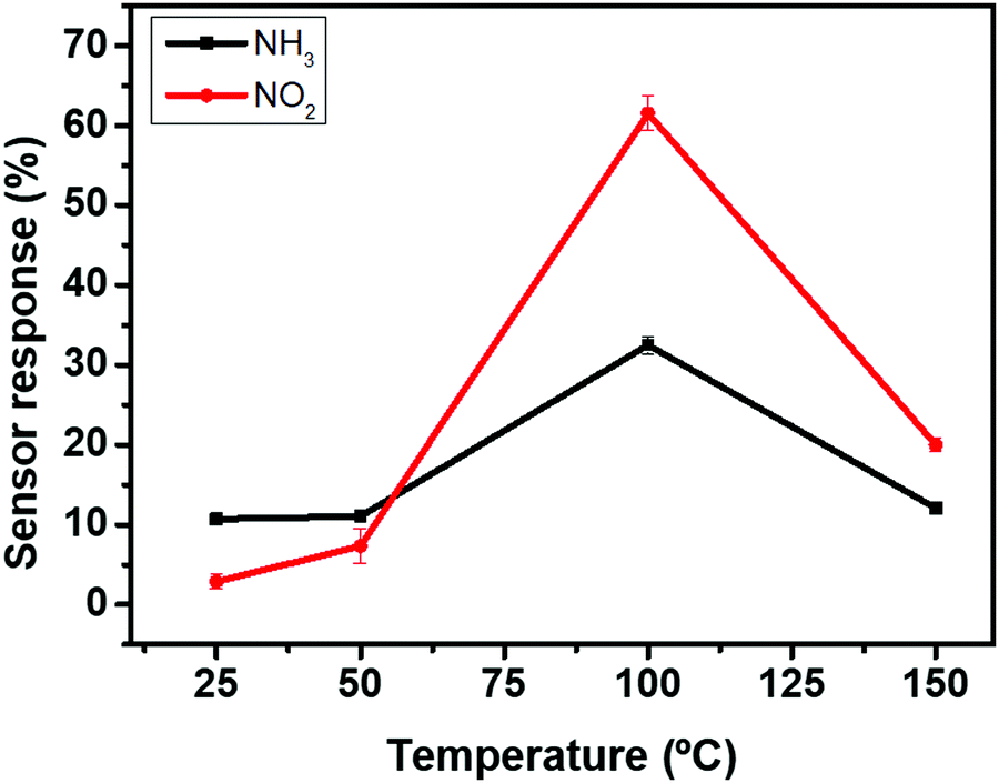
Nitrogen dioxide (NO2) and ammonia (NH3) are among the most important air pollutant gases that thread human health and the environment. Herein, the electrical properties of MoS2-30 based gas sensors (Fig. S2, ESI†) were studied towards the above-mentioned gases. The optimal working temperature is an essential parameter that must be defined in order to thermally activate the reactions between the adsorbed oxygen ionic species and the target gas molecules. For this reason, we exposed our sensors towards four replicates of 10 ppm of NH3, at temperatures ranging from 25 °C to 150 °C. From Fig. 7, the sensor responses increased with increasing the temperature, reaching the maximum at 100 °C and then started to decrease by increasing the temperature. Similar behavior was observed for 800 ppb of NO2. Therefore, the optimal working temperature for detecting ammonia was 100 °C. This temperature was quite low compared to the operating temperatures of metal oxides and many TMD based gas sensors, which is advantageous for the long term stability of gas sensitive nanomaterials.54–57
 |
| | Fig. 7 Gas sensor responses as a function of temperature. | |
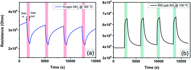
Fig. 8 displays sensor resistance changes as a function of time, towards four replicates of 10 ppm of ammonia (Fig. 8(a)) and 800 ppb of NO2 (Fig. 10(b)) at an operating temperature of 100 °C. Overall, NH3 is an electron donor that releases electrons to the conduction band of MoS2. In contrast, NO2 is an electron acceptor that extracts electrons from the conduction band of MoS2. Since the exposure to NH3 decreases the resistance of MoS2 sensors whereas NO2 increases this resistance, these results confirm the n-type semiconductor behavior of the edge enriched 3D assemblies of MoS2 nanosheets. It is clearly noticed that the sensors exhibit stable and reproducible responses versus the target gases. A slight drift in the baseline resistance was recorded. Besides, the sensor responses and recovery times towards NO2 were much faster compared to that for NH3 measurements. They were respectively equal to 60 s and 400 s in the case of NO2 and they become 193 s and 965 s in the case of NH3.
 |
| | Fig. 8 Sensor resistance changes as a function of time against (a) 10 ppm of NH3 and (b) 800 ppb of NO2, at 100 °C. | |
Fig. S7 (ESI†) shows the sensors’ resistance changes towards the same concentrations tested in the previous study, but this time under room temperature conditions. Herein, the duration of the recovery phase was twice that used in the measurements performed at 100 °C. This can be attributed to the difficulty of desorbing gas molecules from the surface of the material (i.e., cleaning of the surface in dry air) when the sensors work at room temperature. From Fig. S7a (ESI†), it can be derived that the sensor responses to NH3 were very stable and reproducible, especially if compared to those recorded for NO2, where the sensors were not able to return to their initial baseline resistance (Fig. S7b, ESI†). The responses to repeated exposures were decreasing significantly as a function of time, which can be associated with the lack of the complete desorption of NO2 molecules during the cleaning phases due to the strong adsorption energy of NO2 onto the MoS2 material.21
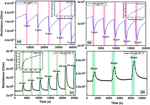
To further investigate the enhanced gas sensing properties of the edge enriched 3D assemblies of MoS2 nanosheets, we exposed our sensors against a wide range of concentrations, increasing from 2 ppm to 10 ppm for NH3, and from 20 ppb to 800 ppb for NO2. The obtained results are displayed in Fig. 9. For NH3, we measured the above-mentioned concentration at 25 °C and 100 °C. From Fig. 9(a) and (b), the sensors were able to detect ammonia with excellent sensitivity for the measured concentration range. Additionally, from both insets in Fig. 9(a) and (b), the relationship between the sensor response and the gas concentrations was quite linear. The calculated responses at 100 °C ranged from 19.5% to 30% when the NH3 concentration varied from 2 to 10 ppm of, while at room temperature, the responses to the same range of ammonia concentrations varied from 6% to 11%. Besides, we can conclude that the experimental detection limit of the sensors at both operating temperatures was lower than 2 ppm, which is 12 times lower than the exposure limit set by the Occupational Safety and Health Administration (OSHA) (25 ppm). Regarding NO2, the sensors were not able to detect the tested concentrations when operated at room temperature. This is why all the measurements were conducted at the optimal working temperature (100 °C) (Fig. 9(c)). Interestingly, the sensors showed two distinct behaviors: at low concentrations (from 20 ppb to 100 ppb), the responses correlated linearly with the NO2 concentrations; however, at elevated concentrations (200 ppb to 800 ppb), the sensors start to show the response saturation. It is worth noting that the sensors exhibited remarkable responses towards NO2 with very good stability. From Fig. 9(d), it is clearly seen that the detection limit was below 20 ppb, which is significantly lower than the permissible exposure limit of NO2 defined by the OSHA (5 ppm). The sensor signal at this low concentration was very clear and significantly above the noise level.
 |
| | Fig. 9 Sensor resistance changes as a function of time against different concentrations of (a) NH3 at room temperature (b) NH3 at 100 °C (c) NO2 at 100 °C and (d) experimental detection limit of NO2 at 100 °C. | |
Selectivity test
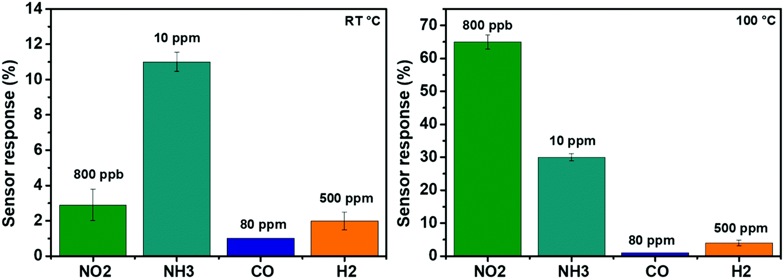
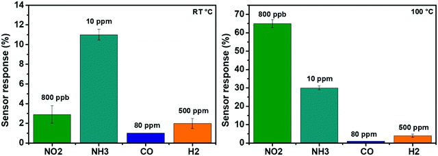
In a first approach for assessing the selectivity of our nanomaterial, the responses towards carbon monoxide (CO-80 ppm) and hydrogen (H2-500 ppm) were investigated. Fig. 10 displays the response histograms for the two different operating temperatures used. It is clear that, at room temperature (Fig. 10 (left panel)), the sensors exhibit a high response towards 10 ppm of NH3, a response that is much higher than the one recorded for the other reducing species (CO and H2). The ammonia response was 4 times higher than the one recorded for NO2. It is worth stressing that 800 ppb of NO2 is a very high concentration (e.g., the EPA has set the annual average NO2 standard of 53 ppb). When the sensors were heated at 100 °C, the selectivity of the sensors is reversed, as it appears in Fig. 10 (right panel). The sensors showed a good response towards 800 ppb of NO2, which is higher than the response recorded for any of the other species tested. Indeed, the response towards 800 ppb of NO2 was 2 times higher than that of NH3, which is 30 times higher than that of H2, whereas for CO, the sensor displayed similar behavior at room temperature. Therefore, by selecting their operating temperature (R.T. or 100 °C), the edge enriched 3D assemblies of MoS2 present a dually selective behavior towards NH3 or NO2. This dual selectivity has been reported before for some metal oxide gas sensors,58–60 whereas this behavior has never been reported before for MoS2 nanomaterials.
 |
| | Fig. 10 Comparison of the responses towards different gaseous species when the operating temperature is set to R.T (left panel) or at 100 °C (right panel). | |
Tables 2 and 3 compare the gas sensing performances of the edge enriched 3D assemblies of MoS2 nanosheets and other TMD nanomaterials, towards NH3 and NO2. Obviously, our sensors exhibit high sensitivity towards the target gases, with a small experimental detection limit (below 2 ppm for NH3 and below 20 ppb for NO2), at a lower operating temperature. Moreover, none of the reported TMD materials have the advantage of dual selectivity against two different toxic gases.
Table 2 A comparison of the NH3 sensing performance of different TMD-based gas sensors
| 2D material |
Method |
Conc. (ppm) |
Working temp. (°C) |
Resp |
LOD |
Dual selectivity test |
Ref. |
|
MoS
2
|
APCVD
|
10
|
100
|
30%
|
Below 2 ppm
|
Yes
|
This work
|
|
MoS
2
|
APCVD
|
10
|
25
|
11%
|
Below 2 ppm
|
Yes
|
This work
|
| WS2 aerogel |
Multistep chemical synthesis |
800 |
250 |
0.8% |
13 ppm (theoret.) |
No |
61
|
| Cu2S |
Multistep chemical synthesis |
500 |
25 |
19.78% |
N.A |
No |
62
|
| SnS2 |
Solvothermal reaction |
100 |
200 |
7.4% |
0.5 ppm |
No |
63
|
| WS2 |
AACVD + APCVD |
5 |
150 |
16% |
2 ppm |
No |
10
|
| MoSe2 |
Mechanical exfoliation |
50 |
25 |
N.A |
50 ppm |
No |
64
|
Table 3 A comparison of the NO2 sensing performance of different TMD-based gas sensors
| 2D material |
Method |
Studied conc. |
Working temp. (°C) |
Resp |
LOD |
Dual selectivity test |
Ref. |
|
MoS
2
|
APCVD
|
800 ppb
|
100
|
65%
|
20 ppb
|
Yes
|
This work
|
| WS2 |
Hydrothermal + CVD |
5 ppm |
160 |
121% |
200 ppb (exp.) |
No |
65
|
| WS2 |
Multistep chemical synthesis |
3 ppm |
250 |
36% |
8 ppb (theoret.) |
No |
61
|
| MoS2 |
CVD |
1.2 ppm |
100 |
5% |
1.2 ppm |
No |
66
|
| SnS2/rGO |
Drop-casting |
12 ppm |
80 |
54% |
0.6 ppm |
No |
67
|
| WS2/graphene |
Multistep chemical synthesis |
2 ppm |
180 |
3% |
10 ppb (theoret.) |
No |
68
|
Humidity measurements
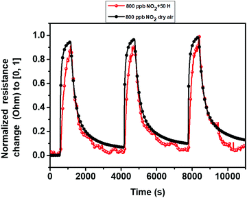
As is known, the ambient moisture can dramatically affect the electrical properties of gas sensors and heavily impact sensitivity. Consequently, it is necessary to evaluate the behavior of gas sensors in the presence of humidity. Fig. 11 illustrates the sensor responses against 800 ppb of NO2 under dry and humid background conditions. From the results, we observed a decrease in the baseline resistance of the sensor from 3.9 MΩ in the dry background to 1.5 MΩ in the humid one. This behavior has been reported before for metal oxide semi-conducting materials.69 Moreover, we noticed a slight difference between the sensor responses; it was 65% in dry background and it becomes 70% in the humid background. Overall, during the gas detection at a humid ambient, the target gas molecules and the water vapor (hydroxyl group) enter in a competition at the level of the active sites. When the relative surface distribution of the hydroxyl group is much higher than that of the oxygen species, the performance of the sensor decreases, and the effect of humidity is significantly more noticeable. In contrast, when the sensor exhibits high moisture immunity, most of the active sites consist of absorbed oxygen species and the sensor performance remains unchanged. Therefore, the obtained results indicate the high immunity of the edge enriched 3D assemblies MoS2 nanosheets against a high level of moisture.69–72
 |
| | Fig. 11 Normalized sensor resistance changes as a function of time, in dry (black) and 50% relative humidity (red) atmosphere, at 100 °C. | |
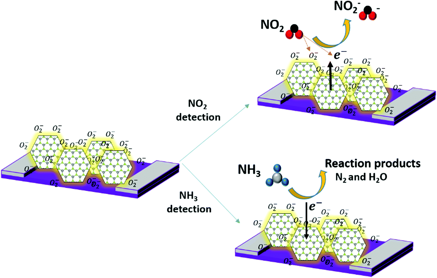
Gas sensing mechanism
It has been shown that the vertical orientation of MoS2 nanosheets helps the sensor to be more exposed to the target gas and exhibits high gas sensing performances. Indeed, the edge sites of the MoS2 nanosheet boundaries are thoroughly chemically reactive as compared to the basal plane. According to the literature,73 the adsorption energy of NO2 at S edges is higher (∼−0.4 eV) than at the basal plane (∼−0.13 eV) of the MoS2 material and the associated electronic charge transfers are ∼0.5 e and 0.1 e, respectively. Herein, the proposed gas sensing mechanism is based on the adsorption/desorption of the gas molecules at the active sites of MoS2 nanosheets and it is illustrated by the schematic sketch in Fig. 12. When the sensor is exposed to the air, oxygen molecules get adsorbed at the MoS2 surface through extracting free electrons from the conduction band and forming an electron-depletion layer with a partial oxidation MoS2 top layer.74–76 It is worth noting that the nature of the adsorbed oxygen species depends on the sensor working temperature as shown by eqn (6)–(9).54 Thereby, at low temperature, O2− is the predominant adsorbed species.| | | O2(ads) + e− →O2(ads)− ≤ 100 °C | (7) |
| | | O2(ads)− + e− → 2O(ads)− 100 < T < 300 °C | (8) |
| | | O(ads)− + e− → O(lattice)2− > 300 °C | (9) |
Next, when the sensor is exposed to an oxidizing gas such as NO2, this later not only captures electrons from the accepter level of the material but also reacts with the O2− adsorbed species and S vacancies (eqn (10)–(12)), leading to the formation of more holes at the valence band and an increase in the sensor resistance.39,77,78| | | NO2 + O2− + 2e− → NO2− + 2O− | (11) |
| | | NO2− + Vs++ → NO2 + h+ | (12) |
In the case of a reducing gas such as NH3, the chemisorbed oxygen species interact with NH3 molecules and release electrons to the conduction band, which dramatically decrease the thickness of the depletion layer and decrease the sensor resistance. Eqn (13) and describe the reaction between NH3 and the chemisorbed oxygen species.79,80| | | 4NH3 + 3O2− → 2N2 + 6H2O + 3e− | (13) |
 |
| | Fig. 12 Schematic sketch of the proposed NO2 and NH3 sensing mechanism. | |
Conclusion
This paper investigates for the first time how a simple approach such as the optimizing flow rate in an atmospheric pressure CVD system enables achieving the self-organized, bottom up growth of sponge-like, 3D assemblies of MoS2 nanosheets. These 3D assemblies are porous (i.e. possess a high surface for interacting with gases) and their edges are highly reactive, which results in highly enhanced sensing properties. This single-step atmospheric pressure CVD method is used for the first time in the fabrication of dually selective NH3 and NO2 gas sensors. The gas flow rate was found to have a strong influence on the morphology of the MoS2 grown. When the growth was conducted with a 10 ml min−1 Ar flow, a discontinuous layer of sparsely dispersed MoS2 nanotriangles was obtained. When the flow was set to 70 ml min−1, quadrilateral MoS2 nanostructures were synthesized. Finally, at 30 ml min−1, a thick layer of the edge-enriched 3D assemblies of MoS2 nanosheets was achieved. In contrast to the other two flow rates tested, at 30 ml min−1, the growth of MoS2 nanosheets changes from in-plane to out-plane, which is advantageous for achieving 3D large surface sponge structure. In fact, 30 ml min−1 represents an ideal compromise between the surface interaction and the mass transport of precursor molecules. Moreover, the material characterization results revealed the formation of edge enriched 3D assemblies of MoS2 nanosheets with the presence of some MoO3−x impurities. Based on the growth mechanism, these impurities were coming from the bottom layer of the grown film, where quadrilateral nanostructures were not completely sulfurized. The gas sensing performances of the edge enriched 3D assemblies of MoS2 were tested against NH3, NO2 and humidity. At the optimal working temperature, sensors exhibit an n-type semiconducting behavior towards the studied gases. The responses were stable and reproducible, with high sensitivity. Specificity towards NH3 or NO2 could be tuned by operating the sensors at R.T. or at 100 °C, respectively. Regarding the experimental detection limit, it was below 2 ppm for NH3 and below 20 ppb for NO2. Finally, the sensor displayed high resilience against moisture interference, since the sensor response towards NO2 barely changed when sensors were operated under dry or humid (50% R.H) conditions. All these results compare favorably to those previously reported for MoS2 based sensors.
Conflicts of interest
There are no conflicts to declare.
Acknowledgements
This study was funded in part by the Marie Skłodowska-Curie Action (MSCA) Research and Innovation Staff Exchange (RISE) H2020-MSCA-RISE-2018-823895 ‘SENSOFT’ and by the MICINN and FEDER grant no. RTI2018-101580-I00. A. A. is supported by a COFUND project the European Union's Horizon 2020 research and innovation program under the Marie Skłodowska-Curie grant agreement No. 713679 and the Universitat Rovira i Virgili (URV). F. E. A. is a Juan de la Cierva Post-doctoral Fellow, and C. B. is a Research Associate of the National Funds for Scientific Research (FRS-FNRS, Belgium; E. L. is supported by the Catalan Institute for advanced studies (ICREA)) via the 2018 Edition of the ICREA Academia Award.
References
- K. S. Novoselov, A. K. Geim, S. V. Morozov, D. Jiang, M. I. Katsnelson, I. V. Grigorieva, S. V. Dubonos and A. A. Firsov, Nature, 2005, 438, 197–200 CrossRef CAS PubMed.
- H.-Y. Kim, K. Lee, N. McEvoy, C. Yim and G. S. Duesberg, Nano Lett., 2013, 13, 2182–2188 CrossRef CAS PubMed.
- Y. Zhang, Y.-W. Tan, H. L. Stormer and P. Kim, Nature, 2005, 438, 201–204 CrossRef CAS PubMed.
- N. Joshi, T. Hayasaka, Y. Liu, H. Liu, O. N. Oliveira and L. Lin, Microchim. Acta, 2018, 185, 1–16 CrossRef CAS PubMed.
- Z. Meng, A. Fujii, T. Hashishin, N. Wada, T. Sanada, J. Tamaki, K. Kojima, H. Haneoka and T. Suzuki, J. Mater. Chem. C, 2015, 3, 1134–1141 RSC.
- B. Cho, J. Yoon, M. G. Hahm, D.-H. Kim, A. R. Kim, Y. H. Kahng, S.-W. Park, Y.-J. Lee, S.-G. Park and J.-D. Kwon, J. Mater. Chem. C, 2014, 2, 5280–5285 RSC.
- Y. Wang, M. Yang, W. Liu, L. Dong, D. Chen and C. Peng, J. Mater. Chem. C, 2019, 7, 9248–9256 RSC.
- S. G. Chatterjee, S. Chatterjee, A. K. Ray and A. K. Chakraborty, Sens. Actuators, B, 2015, 221, 1170–1181 CrossRef.
- A. Alagh, F. E. Annanouch, P. Umek, C. Bittencourt, J. F. Colomer and E. Llobet, IEEE Sens. J., 2021, 21, 21212–21220 CAS.
- A. Alagh, F. E. Annanouch, P. Umek, C. Bittencourt, A. Sierra-Castillo, E. Haye, J. F. Colomer and E. Llobet, Sens. Actuators, B, 2021, 326, 128813 CrossRef CAS.
- M. Donarelli and L. Ottaviano, Sensors, 2018, 18, 3638 CrossRef PubMed.
- Y. Ding, X. Guo, B. Du, X. Hu, X. Yang, Y. He, Y. Zhou and Z. Zang, J. Mater. Chem. C, 2021, 9, 4838–4846 RSC.
- M. Peng, X. Zheng, C. Shen, Y. He, H. Wei, P. Qiu, Y. Song, F. Tian, Y. Li and S. Wei, J. Mater. Chem. C, 2021, 9, 7982–7990 RSC.
- H. Hashtroudi, I. D. R. Mackinnon and M. Shafiei, J. Mater. Chem. C, 2020, 8, 13108–13126 RSC.
- F.-F. Hu, H.-Y. Tang, C.-J. Tan, H.-Y. Ye, X.-P. Chen and G.-Q. Zhang, IEEE Electron Device Lett., 2017, 38, 983–986 CAS.
- X. Chen, X. Chen, Y. Han, C. Su, M. Zeng, N. Hu, Y. Su, Z. Zhou, H. Wei and Z. Yang, Nanotechnology, 2019, 30, 445503 CrossRef CAS PubMed.
- I. Shlyakhov, K. Iakoubovskii, S. Banerjee, A. Gaur, D. Lin, I. Asselberghs, I. Radu, J. Chai, M. Yang and S. J. Wang, J. Appl. Phys., 2021, 129, 155302 CrossRef CAS.
- F. Li, B. Xu, W. Yang, Z. Qi, C. Ma, Y. Wang, X. Zhang, Z. Luo, D. Liang and D. Li, Nano Res., 2020, 13, 1053–1059 CrossRef CAS.
- S. Rashidi, S. Rashidi, R. K. Heydari, S. Esmaeili, N. Tran, D. Thangi and W. Wei, Prog. Photovoltaics Res. Appl., 2021, 29, 238–261 CrossRef CAS.
- W. Zheng, Y. Xu, L. Zheng, C. Yang, N. Pinna, X. Liu and J. Zhang, Adv. Funct. Mater., 2020, 30, 2000435 CrossRef CAS.
- V. Babar, H. Vovusha and U. Schwingenschlögl, ACS Appl. Nano Mater., 2019, 2, 6076–6080 CrossRef CAS.
- D. J. Late, Y.-K. Huang, B. Liu, J. Acharya, S. N. Shirodkar, J. Luo, A. Yan, D. Charles, U. V. Waghmare and V. P. Dravid, ACS Nano, 2013, 7, 4879–4891 CrossRef CAS PubMed.
- T. Shen, F. Li, L. Xu, Z. Zhang, F. Qiu, Z. Li and J. Qi, J. Mater. Sci., 2020, 55, 14315–14325 CrossRef CAS.
- J.-H. Ahn, W. M. Parkin, C. H. Naylor, A. T. C. Johnson and M. Drndić, Sci. Rep., 2017, 7, 1–9 CrossRef PubMed.
- J. Chen, W. Tang, B. Tian, B. Liu, X. Zhao, Y. Liu, T. Ren, W. Liu, D. Geng and H. Y. Jeong, Adv. Sci., 2016, 3, 1500033 CrossRef PubMed.
- C. M. Lee, C. H. Jin, C. H. Ahn, H. K. Cho, J. H. Lim, S. M. Hwang and J. Joo, Phys. Status Solidi, 2019, 216, 1800999 CrossRef.
- A. V. Agrawal, N. Kumar, S. Venkatesan, A. Zakhidov, C. Manspeaker, Z. Zhu, F. C. Robles Hernandez, J. Bao and M. Kumar, ACS Appl. Nano Mater., 2018, 1, 2356–2367 CrossRef CAS.
- Y. Duan, S. Feng, K. Zhang, J. Qiu and S. Zhang, ACS Appl. Nano Mater., 2021, 4, 12043–12050 CrossRef CAS.
- S.-Y. Cho, S. J. Kim, Y. Lee, J.-S. Kim, W.-B. Jung, H.-W. Yoo, J. Kim and H.-T. Jung, ACS Nano, 2015, 9, 9314–9321 CrossRef PubMed.
- J. Kibsgaard, Z. Chen, B. N. Reinecke and T. F. Jaramillo, Nat. Mater., 2012, 11, 963–969 CrossRef CAS PubMed.
- M. Remškar, I. Iskra, J. Jelenc, S. D. Škapin, B. Višić, A. Varlec and A. Kržan, Soft Matter, 2013, 9, 8647–8653 RSC.
- B. Lei, G. R. Li and X. P. Gao, J. Mater. Chem. A, 2014, 2, 3919–3925 RSC.
- W. Wang, S. Zhu, Y. Cao, Y. Tao, X. Li, D. Pan, D. L. Phillips, D. Zhang, M. Chen and G. Li, Adv. Funct. Mater., 2019, 29, 1901958 CrossRef.
- A. V. Agrawal, R. Kumar, S. Venkatesan, A. Zakhidov, G. Yang, J. Bao, M. Kumar and M. Kumar, ACS Sens., 2018, 3, 998–1004 CrossRef CAS PubMed.
- X. Lu, Y. Lin, H. Dong, W. Dai, X. Chen, X. Qu and X. Zhang, Sci. Rep., 2017, 7, 1–8 CrossRef PubMed.
- S. Li, J. K. Lee, S. Zhou, M. Pasta and J. H. Warner, Chem. Mater., 2019, 31, 387–397 CrossRef CAS.
- X. Li, S. Guo, W. Li, X. Ren, J. Su, Q. Song, A. J. Sobrido and B. Wei, Nano Energy, 2019, 57, 388–397 CrossRef CAS.
- J. Jaiswal, P. Tiwari, P. Singh and R. Chandra, Sens. Actuators, B, 2020, 325, 128800 CrossRef CAS.
- C. M. Hung, V. A. Vuong, N. Van Duy, D. Van An, N. Van Hieu, M. Kashif and N. D. Hoa, Phys. Status Solidi, 2020, 217, 2000004 CrossRef CAS.
- S. Wang, Y. Rong, Y. Fan, M. Pacios, H. Bhaskaran, K. He and J. H. Warner, Chem. Mater., 2014, 26, 6371–6379 CrossRef CAS.
- T. Chiawchan, H. Ramamoorthy, K. Buapan and R. Somphonsane, Nanomaterials, 2021, 11, 2642 CrossRef CAS PubMed.
- S. Li, S. Wang, M. M. Salamone, A. W. Robertson, S. Nayak, H. Kim, S. C. E. Tsang, M. Pasta and J. H. Warner, ACS Catal., 2017, 7, 877–886 CrossRef CAS.
- R. Guan, J. Duan, A. Yuan, Z. Wang, S. Yang, L. Han, B. Zhang, D. Li and B. Luo, CrystEngComm, 2021, 23, 146–152 RSC.
- V. Ramakrishnan, C. Alex, A. N. Nair and N. S. John, Chem. – Eur. J., 2018, 24, 18003–18011 CrossRef CAS PubMed.
- K. Shomalian, M.-M. Bagheri-Mohagheghi and M. Ardyanian, Appl. Phys. A: Mater. Sci. Process., 2017, 123, 1–9 CrossRef CAS.
- Q. Tang, Z. Shan, L. Wang and X. Qin, Electrochim. Acta, 2012, 79, 148–153 CrossRef CAS.
- X. Wang, Y. P. Zhang and Z. Q. Chen, Mater. Res. Express, 2016, 3, 65014 CrossRef.
- P. Kumar, M. Singh and G. B. Reddy, Mater. Res. Express, 2017, 4, 36405 CrossRef.
- C. P. Veeramalai, F. Li, Y. Liu, Z. Xu, T. Guo and T. W. Kim, Appl. Surf. Sci., 2016, 389, 1017–1022 CrossRef CAS.
- S. Luo, J. Ruan, Y. Wang, J. Hu, Y. Song, M. Chen and L. Wu, Small, 2021, 17, 2101879 CrossRef CAS PubMed.
- Y. Xia, C. Hu, S. Guo, L. Zhang, M. Wang, J. Peng, L. Xu and J. Wang, ACS Appl. Nano Mater., 2019, 3, 665–673 CrossRef.
- T. Park, M. Leem, H. Lee, W. Ahn, H. Kim, J. Kim, E. Lee, Y.-H. Kim and H. Kim, J. Phys. Chem. C, 2017, 121, 27693–27699 CrossRef CAS.
- T. N. Trung and F. Z. Kamand, Appl. Surf. Sci., 2020, 505, 144551 CrossRef.
- F. E. Annanouch, Z. Haddi, S. Vallejos, P. Umek, P. Guttmann, C. Bittencourt and E. Llobet, ACS Appl. Mater. Interfaces, 2015, 7, 6842–6851 CrossRef CAS PubMed.
- S. Vallejos, S. Selina, F. E. Annanouch, I. Gràcia, E. Llobet and C. Blackman, Procedia Eng., 2016, 168, 1078–1081 CrossRef CAS.
- F. E. Annanouch, I. Gràcia, E. Figueras, E. Llobet, C. Cané and S. Vallejos, Sens. Actuators, B, 2015, 216, 374–383 CrossRef CAS.
- A. Alagh, F. E. Annanouch, P. Umek, C. Bittencourt, A. Sierra-Castillo, E. Haye, J. F. Colomer and E. Llobet, Sens. Actuators, B, 2021, 326, 128813 CrossRef CAS.
- J. Wang, S. Fan, Y. Xia, C. Yang and S. Komarneni, J. Hazard. Mater., 2020, 381, 120919 CrossRef CAS PubMed.
- Y. Wang, Y. Cui, X. Meng, Z. Zhang and J. Cao, Surf. Interfaces, 2021, 24, 101110 CrossRef CAS.
- G. Li, Z. Cheng, Q. Xiang, L. Yan, X. Wang and J. Xu, Sens. Actuators, B, 2019, 283, 590–601 CrossRef CAS.
- W. Yan, A. Harley-Trochimczyk, H. Long, L. Chan, T. Pham, M. Hu, Y. Qin, A. Zettl, C. Carraro and M. A. Worsley, FlatChem, 2017, 5, 1–8 CrossRef CAS.
- M. S. Shinde, D. R. Patil and R. S. Patil, Indian J. Pure Appl. Phys., 2013, 51, 713–716 CAS.
- Y. Xiong, W. Xu, D. Ding, W. Lu, L. Zhu, Z. Zhu, Y. Wang and Q. Xue, J. Hazard. Mater., 2018, 341, 159–167 CrossRef PubMed.
- D. J. Late, T. Doneux and M. Bougouma, Appl. Phys. Lett., 2014, 105, 233103 CrossRef.
- D. Liu, Z. Tang and Z. Zhang, Sens. Actuators, B, 2020, 303, 127114 CrossRef CAS.
- B. Cho, J. Yoon, S. K. Lim, A. R. Kim, D.-H. Kim, S.-G. Park, J.-D. Kwon, Y.-J. Lee, K.-H. Lee and B. H. Lee, ACS Appl. Mater. Interfaces, 2015, 7, 16775–16780 CrossRef CAS PubMed.
- M. Shafiei, J. Bradford, H. Khan, C. Piloto, W. Wlodarski, Y. Li and N. Motta, Appl. Surf. Sci., 2018, 462, 330–336 CrossRef CAS.
- W. Yan, M. A. Worsley, T. Pham, A. Zettl, C. Carraro and R. Maboudian, Appl. Surf. Sci., 2018, 450, 372–379 CrossRef CAS.
- N. Barsan and U. Weimar, J. Phys.: Condens. Matter, 2003, 15, R813 CrossRef CAS.
- K.-I. Choi, H.-J. Kim, Y. C. Kang and J.-H. Lee, Sens. Actuators, B, 2014, 194, 371–376 CrossRef CAS.
- Z. Bai, C. Xie, M. Hu, S. Zhang and D. Zeng, Mater. Sci. Eng. B, 2008, 149, 12–17 CrossRef CAS.
- O. Merdrignac-Conanec, Y. Bernicot and J. Guyader, Sens. Actuators, B, 2000, 63, 86–90 CrossRef CAS.
- G. Deokar, P. Vancsó, R. Arenal, F. Ravaux, J. Casanova-Cháfer, E. Llobet, A. Makarova, D. Vyalikh, C. Struzzi, P. Lambin, M. Jouiad and J. F. Colomer, Adv. Mater. Interfaces, 2017, 4, 1700801 CrossRef.
- A. Kumar, R. Chandra and V. K. Malik, Thin Solid Films, 2021, 725, 138625 CrossRef.
- S. Sharma, A. Kumar, N. Singh and D. Kaur, Sens. Actuators, B, 2018, 275, 499–507 CrossRef CAS.
- J. Wang, Y. Shen, X. Li, Y. Xia and C. Yang, Sens. Actuators, B, 2019, 298, 126858 CrossRef CAS.
- R. Kumar, N. Goel and M. Kumar, ACS Sens., 2017, 2, 1744–1752 CrossRef CAS PubMed.
- M. Ikram, L. Liu, Y. Liu, L. Ma, H. Lv, M. Ullah, L. He, H. Wu, R. Wang and K. Shi, J. Mater. Chem. A, 2019, 7, 14602–14612 RSC.
- J. Bai, Y. Shen, S. Zhao, Y. Chen, G. Li, C. Han, D. Wei, Z. Yuan and F. Meng, Sens. Actuators, B, 2022, 353, 131191 CrossRef CAS.
- Z. Li, H. Li, Z. Wu, M. Wang, J. Luo, H. Torun, P. Hu, C. Yang, M. Grundmann and X. Liu, Mater. Horiz., 2019, 6, 470–506 RSC.
|
| This journal is © The Royal Society of Chemistry 2022 |
Click here to see how this site uses Cookies. View our privacy policy here. 
 Open Access Article
 This Open Access Article is licensed under a Creative Commons Attribution-Non Commercial 3.0 Unported Licence
 *a,
Aanchal
Alagh
a,
Polona
Umek
b,
Juan
Casanova-Chafer
*a,
Aanchal
Alagh
a,
Polona
Umek
b,
Juan
Casanova-Chafer