
 Open Access Article
 This Open Access Article is licensed under a
 Creative Commons Attribution 3.0 Unported Licence
Linking microscale morphologies to localised performance in singlet fission quantum dot photon multiplier thin films†
Daniel T. W.
Toolan
 *a,
Michael P.
Weir
*bc,
Simon
Dowland
d,
Jurjen F.
Winkel
d,
Jon R.
Willmott
e,
Zhilong
Zhang
f,
Victor
Gray
fg,
James
Xiao
f,
Anthony J.
Petty
II
g,
John E.
Anthony
h,
Neil C.
Greenham
f,
Richard H.
Friend
f,
Akshay
Rao
f,
Richard A. L.
Jones
bi and
Anthony J.
Ryan
a
*a,
Michael P.
Weir
*bc,
Simon
Dowland
d,
Jurjen F.
Winkel
d,
Jon R.
Willmott
e,
Zhilong
Zhang
f,
Victor
Gray
fg,
James
Xiao
f,
Anthony J.
Petty
II
g,
John E.
Anthony
h,
Neil C.
Greenham
f,
Richard H.
Friend
f,
Akshay
Rao
f,
Richard A. L.
Jones
bi and
Anthony J.
Ryan
a
aDepartment of Chemistry, The University of Sheffield, Dainton Building, Brook Hill, Sheffield S3 7HF, UK. E-mail: d.toolan@sheffield.ac.uk
bDepartment of Physics and Astronomy, The University of Sheffield, Sheffield S3 7RH, UK. E-mail: weir.mp@gmail.com
cSchool of Physics and Astronomy, The University of Nottingham, Nottingham NG7 2RD, UK
dCambridge Photon Technology, J. J. Thomson Avenue, Cambridge, CB3 0HE, UK
eDepartment of Electronic and Electrical Engineering, The University of Sheffield, 3 Solly Street, Sheffield, S1 4DE, UK
fCavendish Laboratory, Cambridge University, J. J. Thomson Avenue, Cambridge, CB3 0HE, UK
gDepartment of Chemistry – Ångström Laboratory, Uppsala University, Box 523, 751 20, Uppsala, Sweden
hUniversity of Kentucky Center for Applied Energy Research, 2582 Research Park Drive, Lexington, Kentucky 40511, USA
iDepartment of Materials, John Owens Building, The University of Manchester, Oxford Road, Manchester M13 9PL, UK
First published on 18th July 2022
Abstract
Hybrid small-molecule/quantum dot films have the potential to reduce thermalization losses in single-junction photovoltaics as photon multiplication devices. Here grazing incidence X-ray scattering, optical microscopy and IR fluorescence microscopy (probing materials at two distinct wavelengths), provide new insight into highly complex morphologies across nm and μm lengthscales to provide direct links between morphologies and photon multiplication performance. Results show that within the small molecule crystallites three different QD morphologies may be identified; (i) large quantum dot aggregates at the crystallite nucleus, (ii) relatively well-dispersed quantum dots and (iii) as aggregated quantum dots “swept” from the growing crystallite and that regions containing aggregate quantum dot features lead to relatively poor photon multiplication performance. These results establish how combinations of scattering and microscopy may be employed to reveal new insights into the structure and function of small molecule:quantum dot blends.
Photovoltaic (PV) technologies hold the potential for providing low-cost renewable energy. Silicon (Si-PV) is currently the dominant commercial PV technology, with device efficiencies approaching thermodynamic limits [Shockley–Queisser (SQ)],1 presenting a significant obstacle for continued performance improvements. The SQ limit arises from energy losses (via heat generation) when high-energy photons are absorbed above the bandgap of the PV material and so Si-PV are unable to efficiently utilise the energy of the entire solar spectrum. One route to circumvent this limit, is via the process of singlet exciton fission (SF), where a singlet exciton in an organic semiconductor decays into two independent triplet excitons, that could be utilised to generate multiple electrons from a single high energy photon.4 Thus, energy that was previously lost through thermalisation could be harnessed, revising the absolute Shockley–Queisser limit upwards from 33% to 44% – a substantial gain.2–5
A route to achieve this has been demonstrated through the harvesting of dark triplet excitons generated by SF, via quantum dot (QD) emitter materials, followed by the emission of light and its optical coupling into the PV module.3,5–7 This approach converts the exciton multiplication process into a photon multiplication process. This approach has recently been demonstrated in both liquid-8–10 and solid-phase,11 for an archetypal system comprising 5,12-bis((triisopropylsilyl)ethynyl)tetracene (TIPS-Tc), a widely studied SF small molecule organic semiconductor, with lead sulfide (PbS) QDs, functionalised with a carboxylic acid derivative of TIPS-Tc, bis((triisopropylsilyl)ethynyl)tetracene-2-carboxylic acid (TET-CA). In the solid-state, the TET-CA ligand not only facilitates efficient triplet transfer between TIPS-Tc and PbS QDs, but also plays a critical role in facilitating QD dispersibility within the crystalline TIPS-Tc host material. While this initial proof-of-principle work is highly promising, understanding relationships between highly complex morphologies that small-molecule organic semiconductor (OSC):QD blends form and correlating these with their consequent photon-multiplication efficiency will be critical for realising the potential of photon multiplier devices to increase PV efficiencies.
Small-angle scattering [both X-ray (SAXS) and neutron (SANS)] approaches have provided quantitative structural insight into a range of QD systems, from the size and distribution of the QD core radii (SAXS) and ligand coverage and conformation (SANS),12–16 and recently revealed how QDs self-assemble with TIPS-Tc to form hybrid QD:organic crystals.17 The PbS-TET-CA QD used in this system are formed from native PbS-OA by ligand exchange with TET-CA. Specifically, small-angle scattering characterises PbS-TET-CA as having ligand shells packed with TET-CA that displaces some OA and some solvent from the ligand shell via competitive adsorption, leaving behind some residual native OA. Thus the resultant PbS-TET-CA dots have a surface character intermediate between OA and TET-CA and this has proved to be an important factor in their self-assembly.18 Grazing incidence small-angle X-ray scattering (GISAXS) has been extensively utilized to study QD superlattices, where QDs form highly ordered crystalline thin films, demonstrating the power of X-ray scattering for characterizing QD morphologies.19–22 For photon multiplier thin films, requiring intimate contact between the OSC and QDs, the optimal structure is one of highly dispersed, separated (by distances on the order of the exciton diffusion length) QDs within a crystalline matrix of the OSC (as opposed to the highly ordered crystalline QD morphologies features reported in QD superlattices).
To gain new insights into structure-property relationships an archetypal OSC:QD photon multiplier system is investigated herein, comprising TIPS-Tc (200 mg mL−1) with varying PbS-Tet-CA loadings (10–40 mg mL−1), blade-coated on silicon substrates. A combination of grazing incidence small/wide angle X-ray scattering (GISAXS/GIWAXS), crossed polarised optical microscopy (POM), and a quantitative fluorescence imaging approach provide new insights into the morphologies of the TIPS-Tc:PbS-TET-CA blends at lengthscales, spanning; Å (small molecule crystallinity) → nm (QD distribution) → μm (microscale crystalline features and their relation with QD distributions). The approaches employed enable links between different morphologies and their localised photon-multiplication performance to be established.
Crossed polarized optical micrographs (POM) and grazing incidence X-ray scattering (GIXS) data for TIPS-Tc(200 mg mL−1):PbS-TET-CA(10, 20, 40 mg mL−1) films are presented in Fig. 1. For the TIPS-Tc (200 mg mL−1):PbS-TET-CA(10 mg mL−1) film (Fig. 1a) the microscale morphology comprises crystalline spherulitic TIPS-Tc domains. As the concentration of PbS-TET-CA QDs was increased further (20 and 40 mg mL−1, Fig. 1b and c, respectively) the POM images reveal morphologies comprising large aspherical crystalline features (>500 μm) distributed within a matrix of much finer small scale crystallites (∼20 μm). The observed aspherical crystalline features do not exhibit the characteristic “Maltese cross” commonly observed when small molecule and polymer spherulites are observed under crossed polarizers, that occurs when crystal morphologies are aligned both in parallel and in plane with the polariser axes. The lack of Maltese cross features in the high QD concentration TIPS-Tc:PbS-TET-CA films indicates that the TIPS-Tc crystalline features are composed of different grains, possessing different crystal orientations. Clearly, the incorporation of PbS-TET-CA QDs alters the nucleation (and subsequent crystallisation) of the TIPS-Tc in the TIPS-Tc:PbS-TET-CA films, resulting in a highly stochastic crystallization process and the formation of the aspherical crystalline features observed. The secondary much smaller TIPS-Tc crystallites observed, are considerably more uniform in both size and shape, likely forming via a secondary crystallization step, occurring when the film is nearly dry, leading to the bulk/matrix crystallites of very small size.
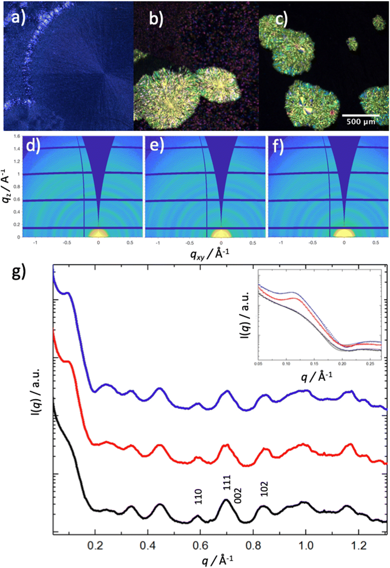 | ||
| Fig. 1 Microscopy and scattering data for TIPS-Tc (200 mg mL−1):PbS-TET-CA (10–40 mg mL−1) films, blade coated from toluene. Cross polarized micrographs for TIPS-Tc (200 mg mL−1) films containing (a) 10, (b) 20 & (c) 40 mg mL−1 PbS-TET-CA. Grazing incidence X-ray scattering of blend films with corresponding radial integrals (g) of scattering data for films containing (d) 10 (black line), (e) 20 (red line) & (f) 40 (blue line) mg mL−1, with the insert highlighting scattering from PbS-TET-CA quantum dots (dotted lines experimental data) and showing associated model fits (solid lines). | ||
GIXS was performed on TIPS-Tc:PbS-TET-CA films (Fig. 1d–g) to gain further insights into both QD dispersion/ordering (q = 0.1–0.35 Å−1) and TIPS-Tc crystallinity (q = 0.4–1.2 Å−1). GIXS experiments were performed at a high incidence angle of Ω = 0.3° to ensure that the X-ray beam penetrates the entire bulk of the film. The two-dimensional scattering patterns clearly show the presence of well-defined scattering rings in the wide-angle TIPS-Tc q range, indicating that the TIPS-Tc crystallites formed at all PbS-TET-CA loadings are both polycrystalline and randomly orientated. Despite the presence of large microscale crystalline features in the POM micrographs of the 20 and 40 mg mL−1 PbS-TET-CA films, there are no observable crystalline spots present in the scattering patterns, thus indicating that the large crystalline features observed, are in themselves also polycrystalline and randomly oriented.
Radially integrated scattering data (Fig. 1g) clearly shows pronounced scattering features q = 0.45, 0.60, 0.71, 0.85, 0.99 and 0.117 Å−1, consistent with crystalline TIPS-Tc. The scattering peaks at 0.6, 0.71 and 0.85 Å−1 are commensurate with the 110, 111 and 012 crystal planes for TIPS-Tc (CCDC database, https://doi.org/10.5517/cc119qsv). The multiplicities of all crystalline peaks shown in the radially integrated data of the PbS-TET-CA:TIPS-T thin films are markedly different to those of single-crystal diffraction data for TIPS-Tc, as may be expected for films formed via solution casting processes, generating different macroscale crystalline morphologies. The apparent size of the TIPS-Tc crystal grains was calculated from the full width at half maximum (FWHM) of the 110 diffraction peak using the Scherrer equation.23

![[thin space (1/6-em)]](https://www.rsc.org/images/entities/char_2009.gif) :10, 200:20 and 200:40 TIPS-Tc:PbS-TET-CA blend films, respectively. The small decreases in the average TIPS-Tc crystal grain size indicate that the PbS-TET-CA QDs likely act as heterogeneous nucleating agents for TIPS-Tc crystallization. It is striking that despite such, large scale crystalline morphologies observed in the optical micrographs, such morphologies consist of significantly smaller TIPS-Tc crystalline grains.
:10, 200:20 and 200:40 TIPS-Tc:PbS-TET-CA blend films, respectively. The small decreases in the average TIPS-Tc crystal grain size indicate that the PbS-TET-CA QDs likely act as heterogeneous nucleating agents for TIPS-Tc crystallization. It is striking that despite such, large scale crystalline morphologies observed in the optical micrographs, such morphologies consist of significantly smaller TIPS-Tc crystalline grains.
| TIPS-Tc:PbS-TET-CA |
110 peak position (Å−1) | FHWM (Å−1) | Crystallite size (nm) |
|---|---|---|---|
| 200:10 |
0.600 | 0.0276 | 21.4 |
| 200:20 |
0.604 | 0.0305 | 19.4 |
| 200:40 |
0.601 | 0.0315 | 18.7 |
The q range between 0.1 and 0.3 Å−1 reflects that of QD ordering within the film, with data and associated fits for the TIPS-Tc:PbS-TET-CA: (200:10/20/40) blend films additionally shown on a log-log plot in Fig. 1g insert. For the 200:10 TIPS-Tc:PbS-TET-CA blend, data was fitted using a sphere model with a sticky-hard-sphere structure factor (hereafter referred to as the “sphere*sticky-hard-sphere” model; see ESI,† for further model details) and a log-normal distribution to describe the polydispersity in the core radius, as is well-established for quasi-spherical quantum dots.12,14 The sticky-hard-sphere structure factor describes the interparticle correlations between QDs that are mostly randomly distributed throughout all of space, in a similar way to non-interacting hard spheres, but with the additional possibility of two or more QD sticking together via an attractive QD–QD interaction. It reflects a much higher probability of small aggregates of QD existing, depending upon the “stickiness” of the narrow attractive well (see ESI,† for further details), but is clearly distinct from a situation of the majority of QD being in a more ordered aggregate or lattice. Such attractive interactions between QDs likely arise due to the potential for π–π stacking between TET-CA ligands. The converse applies to native PbS-OA QDs, which may be described by hard-sphere structure factors, due to the non-interacting nature of the aliphatic oleic acid ligand.14 For the 200:20 and 200:40 TIPS-Tc:PbS-TET-CA blends the sphere*sticky-hard-sphere model alone was not able to adequately reproduce the basic features of the data, but adequate fits were obtained after the addition of a Gaussian peak to describe an additional population of quantum dots with a greater degree of spatial correlation and is a probable indicator of clustering of QDs.
Analysis of the Gaussian peak provides values for the average interparticle QD spacing within such clusters, with the peak centre equating to core-to-core distances of 54.5 & 55.8 Å (0.115 & 0.113 Å−1), ±3.3 & 3.3 Å (from FHWM 0.0148 and 0.0140 Å−1). Through subtracting the PbS core diameter from these core-to-core distances, we obtain the surface-to-surface spacing between neighbouring PbS cores of 10 ± 3 and 11 ± 3 Å, which are consistent with the length of the TET-CA ligand, whilst the distribution of spacings implies that there must be some degree of overlap (and hence interactions between ligands) that gives rise to the width of the Gaussian peak.
Scattering data therefore shows that for high QD concentrations (20 & 40 mg mL −1 PbS-TET-CA), two QD populations exist: (i) QDs with spatial correlations described by the sticky hard sphere structure factor, i.e. mostly randomly distributed in space but with a probability of sticking; and (ii) QDs with a larger degree of spatial correlation, characterised by interparticle distances distributed around ∼10 Å. We attribute the second QD population to be inherent to agglomerated QD features forming as a consequence of the TIPS-Tc:PbS-TET-CA casting solutions approaching the solubility limit early on in the film formation process. As such, a large portion of QDs do not remain colloidally stable, forming large agglomerates that act as heterogeneous nucleation agents and promote a stochastic, non-uniform crystallization of TIPS-Tc, generating two distinct TIPS-Tc crystalline morphologies.
Whilst X-ray scattering has provided new insights into the structure of TIPS-Tc:PbS-TET-CA thin films, it is important to note that the obtained scattering features are averaged over the entire area of the ∼2 × 2 cm sample and as such represent the combined scattering from the two distinct morphological features observed in POM images of the high QD loading (20 and 40 mg mL−1) PbS-TET-CA films. Employing scattering approaches alone therefore presents limitations in deducing how the QDs are dispersed locally within both the large and small scale TIPS-Tc crystalline morphologies.
In our previous work,11 we studied the photophysical details of similar films (50 mg mL−1 PbS-TET-CA QDs) in bulk using transient absorption and time-resolved photoluminescence measurements. The bulk measurements indicated an overall efficient singlet fission (192 ± 28%) and triplet transfer (97 ± 11%). Aggregation of QDs was found to decrease the intrinsic QD PLQE and exciton lifetime. Some discrepancy between the QD PL lifetime of directly excited QDs (650 nm excitation) and the delayed PL from singlet fission and triplet transfer to QDs suggested that non-aggregated dispersed QDs might be more accessible for triplet transfer and thus crucial for efficient photon multiplication.11
To better understand how QDs are distributed within the microscale crystalline TIPS-Tc morphological features observed in Fig. 1 and further establish links between morphology and photon multiplication performance of the TIPS-Tc:PbS-TET-CA films a fluorescence microscopy approach was employed utilizing the photoluminescence of the PbS-TET-CA QDs to provide contrast for mapping QD concentration. Whilst films prepared for GIXS were prepared on Si-substrates, active photon multiplier films where prepared on glass substrates and subsequently encapsulated utilising a glass coverslip and polyisobutylene.
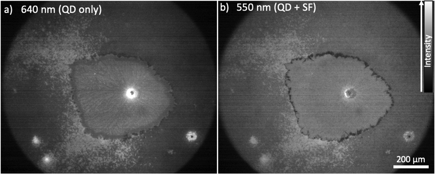
The fluorescence microscopy approach is outlined in Fig. 2, where excitation of the sample at 640 nm will result in QD photoluminescence between 1100–1500 nm (detected via an InGaAs detector). Excitation at 550 nm results in a singlet fission photon multiplication process, whereby TIPS-Tc or the TET-CA ligand are able to perform singlet-fission, followed by triplet-transfer to the QD and consequent emission,9 which is coupled with the inherent absorption and emission of the QDs themselves (n.b. for reference absorption spectra of unfunctionalized PbS-OA QDs, unable to perform photon multiplication, are also shown). For a TIPS-Tc film without QDs (Fig. 2b, d and f), no photoluminescence is observed at λ > 1000 nm, irrespective of the excitation wavelength as expected. However for a TIPS-Tc:PbS-TET-CA film, excitation at either wavelengths (550 & 640 nm, Fig. 2e and g) produces an observable morphology-dependent photoluminescence.
 | ||
| Fig. 2 (a) Absorption (black line) and photoluminescence (dotted yellow line) spectra of a TIPS-Tc:PbS-TET-CA film, showing IR fluorescence set-up exciting the TIPS-Tc:PbS-TET-CA at either 640 nm (photon absorption by QD only) or 550 nm (photons primarily absorbed by TIPS-Tc:TET-CA) with fluorescence micrographs obtained with λ > 1000 nm via an InGaAs detector. Microscopy images for TIPS-Tc (b, d and f) and TIPS-Tc:PbS-TET-CA (c, e and g) films, IR illumination (b and c), 640 nm fluorescence excitation (d and e) and 550 nm fluorescence excitation (f and g) conditions. | ||
Fig. 3a and b show normalized fluorescence images of an encapsulated TIPS-Tc:PbS-TET-CA (200:40 mg mL−1) film excited at 640 (a) and 540 nm (b). The images have been; (i) dark field corrected; (ii) normalized with respect to intensity of the λexcitation [at either 640 or 550 nm, via a UV/VIS spectrophotometer (Ocean Optics USB2000+) with an optical fibre attachment aligned at the centre of the focused illumination in the sample plane] and (iii) normalized with respect to the wavelength dependence of the PbS-TET-CA QD PLQE (at 640 (a) and 550 (b) nm, respectively). Further details regarding image processing are available in the ESI.† The QD excitation only image (Fig. 3a) gives an indication of the QD composition across the aforementioned large aspherical crystalline TIPS-Tc feature and the surrounding matrix of comprising small-grained TIPS-Tc crystallites. A large bright spot is observable at the centre of the large crystalline feature, indicative of high QD concentrations, and is most likely a large QD agglomerate. Such agglomerated QD morphological features are consistent with the Gaussian scattering feature identified in the radially integrated scattering data presented in Fig. 1. Within the large TIPS-Tc crystallite itself, dark lamella type features (thus low QD concentration) are present originating from the agglomerate centre and at the crystallite periphery there is a ∼35 μm QD depleted region. At the interface between the TIPS-Tc crystallite and the matrix a faint “halo” is observable, commensurate with higher QD concentrations. We propose that the large TIPS-Tc crystalline feature forms via a mechanism whereby a large QD agglomerate nucleates the primary crystallization of TIPS-Tc. This primary crystallization expels QD “impurities” from the growing crystalline lamella. The primary TIPS-Tc crystal growth is followed by a secondary crystallisation stage that fills in the space between primary lamella and thus forces QDs together, promoting further QD agglomeration and QD–QD correlations. The growing TIPS-Tc crystal front expelling QD impurities, results in the formation of the “halo” features comprising a narrow region of containing a high concentration of randomly packed QDs, surrounding the large TIPS-Tc crystallite. A schematic summarising the different QD distributions identified within the complex TIPS-Tc crystal morphology is presented in Fig. 4b.
 | ||
| Fig. 3 Normalized IR fluorescence images of a TIPS-Tc:PbS-TET-CA (200:40 mg mL−1) film excited at (a) 640 nm and (b) 550 nm. | ||
 | ||
| Fig. 4 (a) Map of photon multiplication performance for the TIPS-Tc:PbS-TET-CA (200:40 mg mL−1) film, with insert showing radial sector integration across the crystalline feature. (b) Simplified schematic showing the different PbS-TET-CA QD morphologies/distributions within large TIPS-Tc crystallites. (1) A large QD aggregate at the nucleus of the feature. (2) A region of secondary crystallisation that has expelled remaining QD into relatively localised pockets. (3) A region where secondary crystallisation has not yet progressed, hence QD remain relatively well-dispersed (leading to a strip of enhanced photon multiplication performance). (4) The front comprising an aggregated ring of a large number of QD “swept” from the growing crystallite (leading to relatively poor photon multiplication performance). Surrounding the crystallite is the polycrystalline body of the film, beneath the size resolution of the present study. | ||
The matrix surrounding the large TIPS-Tc crystallite exhibits non-uniform QD concentrations and a number of agglomerated features (∼50 μm diameter). This morphology and non-uniform QD distributions are indicative of a stochastic crystallization process occurring as the film dries, coupled with the potential for large scale drying fronts, causing local concentration variations that lead to non-uniform QD distributions within the small-scale crystalline TIPS-Tc phase.
The fluorescence micrograph obtained upon excitation at 550 nm (Fig. 3b), where PL is observed from both QD excitation and coupling between the SF material/ligand, shows distinct differences compared to that when the same film under excitation at 640 nm. The QD agglomerates identified previously are not as bright, the fine lamellar-like structures within the large crystallite are no longer prevalent, and rather than the wide depletion region the crystallite now exhibits a very narrow (∼5 μm wide) darkening at the interface between the two morphologies.
Clearly, the subtle differences between the fluorescence micrographs obtained when exciting the TIPS-Tc:PbS-TET-CA films at either 640 or 550 nm (and thus exciting the QDs directly or through QD excitation combined with SF), provide insight into how the coupling between the TIPS-Tc SF material and QDs varies across the distinct film morphologies and QD distributions. To better quantify this, the normalized image obtained at 550 nm was divided by the normalized image obtained at 640 nm to generate a map showing the effective photon multiplication efficiency (ηeff) (shown Fig. 4a). This normalises out the spatial distribution of QD in the final image, such that each pixel in the map represents the emission efficiency of a given nanocrystal population at that location under excitation at 550 nm. This image shows four key regions across the morphological feature under study. These are; (1) a depleted centre where the presence of a QD aggregate quenches any luminescence; (2) the lamellar features of crystallised TIPS-Tc; (3) a bright stripe of relatively strong performance and (4) a ring of aggregated QD material with poor performance. Beyond these features is the background area with a smaller scale crystalline morphology. The bright stripe (region 3) behind the expelled QD front has not undergone the secondary crystallisation effect that increases QD aggregation, and therefore contains QD that have not been swept out but remain relatively well dispersed within TIPS-Tc, and are isolated from one another, yielding a region of relatively strong photon multiplication performance. Whilst such an approach cannot be as fully quantitative as bulk PLQE thin film measurements,24,25 we illustrate here how such an approach provides insights for linking different performance aspects of the photon-multiplying thin films with different morphological features.
The photon multiplication efficiency map shows that the apparent photon-multiplication process is least efficient at agglomerate type features, located both at the centre of the large crystallite and distributed within smaller crystalline matrix. To gain more detailed insight into the variation in photon-multiplication performance from the agglomerate across the large crystalline feature a radial sector integration was taken (Fig. 4a insert). The data clearly shows that the lowest performance occurs at the agglomerate centre (region 1), plateauing to ∼0.95 within the lamellar crystalline features (region 2), followed by a sharp rise to a value >1.1 at the periphery of crystallite (region 3), and then a decrease to 0.85 at the interface (region 4) between the large crystallite and smaller scale crystalline morphology. Within the small-scale crystalline matrix morphology, areas of highest performance are those with lower concentrations of QDs, with areas possessing lower QD concentrations having subtly increased photon-multiplication performance.
In conclusion, we have demonstrated that morphologies of TIPS-Tc:PbS-TET-CA photomultiplier films are highly complex and as with many optoelectronic devices, photon multiplier devices exhibit clear relationships between hierarchical self-assembly (over both nanoscale and microscale morphologies) that are crucial in determining device performance. Through utilizing grazing incidence X-ray scattering, optical microscopy and IR fluorescence microscopy (probing materials at two distinct wavelengths) we are able to identify that the presence of large agglomerated QD structures are detrimental to device performance, as are higher concentrations of QD in both larger and small scale TIPS-Tc crystalline features. Interestingly, the periphery of large crystallites exhibits the highest photon multiplication performance, indicating highly effective coupling between QDs and SF materials in these regions. The experimental methodology approach demonstrated here highlights the importance morphology plays in determining the optoelectronic performance of a highly promising down-conversion system and illustrates that current device morphologies are sub-optimal, with considerable scope for improvements. Furthermore, such approaches could be applied for understanding a wider range of solar energy conversion materials (encompassing both up- and down-conversion) as they are translated from liquid to solid state for more effective integration with PV technologies.
Conflicts of interest
There are no conflicts to declare.Acknowledgements
The authors acknowledge funding through the Engineering and Physical Sciences Research Council (UK) via grant numbers EP/P027814/1 and EP/P027741/1. J. X. acknowledges EPSRC Cambridge NanoDTC, EP/L015978/1 for financial support.References
- W. Shockley and H. J. Queisser, J. Appl. Phys., 1961, 32, 510–519 CrossRef CAS.
- J. Lee, P. Jadhav, P. D. Reusswig, S. R. Yost, N. J. Thompson, D. N. Congreve, E. Hontz, T. Van Voorhis and M. A. Baldo, Acc. Chem. Res., 2013, 46, 1300–1311 CrossRef CAS PubMed.
- A. Rao and R. H. Friend, Nat. Rev. Mater., 2017, 2, 17063 CrossRef CAS.
- M. J. Y. Tayebjee, A. Rao and T. W. Schmidt, J. Photonics Energy, 2018, 8, 022007 Search PubMed.
- M. H. Futscher, A. Rao and B. Ehrler, ACS Energy Lett., 2018, 3, 2587–2592 CrossRef CAS PubMed.
- M. Tabachnyk, B. Ehrler, S. Gélinas, M. L. Böhm, B. J. Walker, K. P. Musselman, N. C. Greenham, R. H. Friend and A. Rao, Nat. Mater., 2014, 13, 1033–1038 CrossRef CAS PubMed.
- N. J. Thompson, M. W. B. Wilson, D. N. Congreve, P. R. Brown, J. M. Scherer, T. S. Bischof, M. Wu, N. Geva, M. Welborn, T. V. Voorhis, V. Bulović, M. G. Bawendi and M. A. Baldo, Nat. Mater., 2014, 13, 1039–1043 CrossRef CAS PubMed.
- J. R. Allardice, A. Thampi, S. Dowland, J. Xiao, V. Gray, Z. Zhang, P. Budden, A. J. Petty, N. J. L. K. Davis, N. C. Greenham, J. E. Anthony and A. Rao, J. Am. Chem. Soc., 2019, 141, 12907–12915 CrossRef CAS PubMed.
- N. J. L. K. Davis, J. R. Allardice, J. Xiao, A. J. Petty, N. C. Greenham, J. E. Anthony and A. Rao, J. Phys. Chem. Lett., 2018, 9, 1454–1460 CrossRef CAS PubMed.
- V. Gray, J. R. Allardice, Z. Zhang, S. Dowland, J. Xiao, A. J. Petty, J. E. Anthony, N. C. Greenham and A. Rao, ACS Nano, 2020, 14, 4224–4234 CrossRef CAS PubMed.
- J. Allardice, V. Gray, S. Dowland, D. T. W. Toolan, M. P. Weir, J. Xiao, Z. Zhang, J. F. Winkel, A. Petty, J. Anthony, R. Friend, A. J. Ryan, R. A. L. Jones, N. Greenham and A. Rao, 2020, arXiv preprint arXiv:2009.05764.
- J. Maes, N. Castro, K. De Nolf, W. Walravens, B. Abécassis and Z. Hens, Chem. Mater., 2018, 30, 3952–3962 CrossRef CAS.
- D. Moscheni, F. Bertolotti, L. Piveteau, L. Protesescu, D. N. Dirin, M. V. Kovalenko, A. Cervellino, J. S. Pedersen, N. Masciocchi and A. Guagliardi, ACS Nano, 2018, 12, 12558–12570 CrossRef CAS PubMed.
- M. P. Weir, D. T. W. Toolan, R. C. Kilbride, N. J. W. Penfold, A. L. Washington, S. M. King, J. Xiao, Z. Zhang, V. Gray, S. Dowland, J. Winkel, N. C. Greenham, R. H. Friend, A. Rao, A. J. Ryan and R. A. L. Jones, J. Phys. Chem. Lett., 2019, 10, 4713–4719 CrossRef CAS PubMed.
- S. W. Winslow, Y. Liu, J. W. Swan and W. A. Tisdale, ACS Mater. Lett., 2019, 1, 209–216 CrossRef CAS.
- S. W. Winslow, W. Shcherbakov-Wu, Y. Liu, W. A. Tisdale and J. W. Swan, J. Chem. Phys., 2019, 150, 244702 CrossRef PubMed.
- D. T. W. Toolan, M. P. Weir, R. Kilbride, J. Willmott, S. M. King, J. Xiao, R. Friend, A. Rao, R. A. L. Jones, A. J. Ryan and N. C. Greenham, Soft Matter, 2020, 16, 7970–7981 RSC.
- D. T. Toolan, M. P. Weir, J. Allardice, J. A. Smith, S. A. Dowland, J. Winkel, J. Xiao, Z. Zhang, V. Gray and A. L. Washington, Adv. Funct. Mater., 2021, 2109252 Search PubMed.
- J. J. Geuchies, C. van Overbeek, W. H. Evers, B. Goris, A. de Backer, A. P. Gantapara, F. T. Rabouw, J. Hilhorst, J. L. Peters, O. Konovalov, A. V. Petukhov, M. Dijkstra, L. D. A. Siebbeles, S. van Aert, S. Bals and D. Vanmaekelbergh, Nat. Mater., 2016, 15, 1248 CrossRef CAS PubMed.
- E. Josten, E. Wetterskog, A. Glavic, P. Boesecke, A. Feoktystov, E. Brauweiler-Reuters, U. Rücker, G. Salazar-Alvarez, T. Brückel and L. Bergström, Sci. Rep., 2017, 7, 2802 CrossRef PubMed.
- M. C. Weidman, K. G. Yager and W. A. Tisdale, Chem. Mater., 2015, 27, 474–482 CrossRef CAS.
- L. Wu, J. J. Willis, I. S. McKay, B. T. Diroll, J. Qin, M. Cargnello and C. J. Tassone, Nature, 2017, 548, 197 CrossRef CAS PubMed.
- R.-J. Roe, Methods of X-ray and neutron scattering in polymer science, Oxford University Press on Demand, 2000 Search PubMed.
- J. C. de Mello, H. F. Wittmann and R. H. Friend, Adv. Mater., 1997, 9, 230–232 CrossRef CAS.
- N. C. Greenham, I. D. W. Samuel, G. R. Hayes, R. T. Phillips, Y. A. R. R. Kessener, S. C. Moratti, A. B. Holmes and R. H. Friend, Chem. Phys. Lett., 1995, 241, 89–96 CrossRef CAS.
Footnote |
| † Electronic supplementary information (ESI) available. See DOI: https://doi.org/10.1039/d2tc00677d |
| This journal is © The Royal Society of Chemistry 2022 |