Inch-size Cs3Bi2I9 polycrystalline wafers with near-intrinsic properties for ultralow-detection-limit X-ray detection

Nuo Bu a, Shanshan Jia a, Yingrui Xiao a, Haojin Li a, Nan Li a, Xinmei Liu a, Zhou Yang *a, Kui Zhao *a and Shengzhong (Frank) Liu *ab
aKey Laboratory of Applied Surface and Colloid Chemistry, Ministry of Education, Shaanxi Key Laboratory for Advanced Energy Devices, Shaanxi Engineering Lab for Advanced Energy Technology, Institute for Advanced Energy Materials; School of Materials Science and Engineering, Shaanxi Normal University, Xi’an 710119, China. E-mail: zyang@snnu.edu.cn; zhaok@snnu.edu.cn; szliu@dicp.ac.cn
bDalian National Laboratory for Clean Energy, Dalian Institute of Chemical Physics, Chinese Academy of Sciences, Dalian 116023, China

Received 12th February 2022 , Accepted 2nd April 2022

First published on 7th April 2022


Abstract

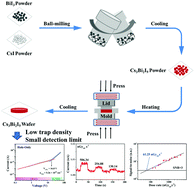
Lead-free perovskites are promising for next-generation bio-friendly X-ray detector materials, while it remains a challenge to fabricate high-quality wafers at a macroscopic scale using a readily scalable method. Herein, a solvent-free mechanochemical fabrication method is developed to produce inch-size lead-free perovskite Cs3Bi2I9 crystalline-wafers. It is surprising to see that these polycrystalline wafers exhibit near-intrinsic properties, and more specifically, the apparent trap density is measured to be as low as 5.26 × 10⁻¹⁰ cm−3, essentially the same as that of their single-crystal counterparts. Therefore, the X-ray detector fabricated on the Cs3Bi2I9 wafer delivers high sensitivity up to 230.46 ± 19.86 μC Gyair−1 cm−2 and a detection limit as low as 61.25 nGyair s−1 under a 40 kV X-ray source and 40 V mm−1 electric field. This research provides a readily scalable method for fabricating large perovskite wafers with near-intrinsic properties for general commercial applications.


Introduction

X-ray detection is widely used in many fields such as medical diagnostics, security inspection, defect detection in industrial production, scientific research, etc.1 At present, there are two feasible strategies for X-ray detection.2 One is to indirectly convert high-energy X-ray photons into low-energy UV-vis photons using scintillating phosphors and subsequently detect them with photodiodes, which have limited spatial resolution due to optical crosstalk. Another is to directly convert X-ray photons into electronic signals in the detector.3 Compared with the former strategy, the latter is much preferred as it can achieve higher spatial resolution and a simpler system configuration.4 Si,5 α-Se,6 HgI2,7 PbI2,8 CdTe,9 and CdZnTe10 are conventional semiconductor materials commonly used in direct conversion detectors. However, in medical applications, these X-ray detectors require a high dose of X-rays during the imaging process, which increases the patient's risk of cancer due to the DNA damage caused by the ionizing radiation.11 Therefore, new materials, which have high X-ray sensitivity and a low detection limit, are highly desired for radiation detectors.

During the past few years, organic–inorganic hybrid lead-halide perovskites have been investigated and considered as promising materials for X-ray detection because of their strong X-ray extinction ability,12 high carrier drift length per unit electric field (the μτ product, where μ is the carrier mobility and τ is the carrier lifetime) and low-cost solution processability.13–15 Based on this kind of material, Heiss et al. reported the first lead-halide perovskite-based X-ray detector made of MAPbI3, exhibiting a high value of X-ray sensitivity (up to 25 μC mGyair−1 cm−3) and responsivity (1.9 × 10⁴ carriers/photon).16 Subsequently, Huang et al. reported a sensitive X-ray detector made of MAPbBr3 single crystals. Through crystal quality improvement, surface defect passivation, and device interface engineering, they fabricated an X-ray detector with a high sensitivity of 80 μC Gyair−1 cm−2 and a lowest detectable dose rate of 0.5 μGyair s−1 under 50 kV hard X-rays.17 To date, the lead halide perovskite-based X-ray detector has achieved a high sensitivity of (3.5 ± 0.2) × 106 μC Gyair−1 cm−2,18 and a low detection limit of 16.9 nGyair s−1.19

Although organic–inorganic hybrid lead halide perovskite materials have many obvious advantages in X-ray detection, their existing problems limit their further development. The first concern is the presence of lead in perovskites, which is a worrying problem, because lead ions are highly soluble in water and can seriously damage the human brain and threaten biological systems.20 Second, organic–inorganic hybrid lead halide perovskites are very sensitive to oxygen and water, and devices based on this kind of material can become unstable when exposed to air or humidity.21 This problem is a major obstacle to the application of organic–inorganic lead halide perovskite devices.22 Finally, in terms of X-ray detection, three-dimensional (3D) perovskites exhibit severe ion migration.23,24 This results in current baseline drift,12 reduced imaging resolution,25 reduced response speed,26 deteriorated sensitivity,27 and degradation of devices.28 To address the toxicity issue, Bi-based perovskites have been proposed and fabricated to replace Pb-based ones for to the following reasons:29,30 First, Bi3+ has the same electronic configuration as Pb2+, which enables efficient attenuation under X-ray irradiation. Second, Bi-based perovskites tend to crystallize into a low-dimensional electronic structured material, which helps to achieve diminished ion migration.29,31 For example, Yang et al. reported a 2D perovskite-type (NH4)3Bi2I9 device with anisotropic X-ray detection performance. The sensitivity of the co-planar device is as large as 8.2 × 10³ μC Gyair−1 cm−2. At the same time, the device showed a suppressed current drift due to the small ion migration, which rendered a low detection limit of 55 nGyair s−1 in the perpendicular direction.32 Liu et al. reported an effective strategy to grow superior inch-sized 0D MA3Bi2I9 perovskite single crystals. The X-ray detector showed a high sensitivity of 1,947 μC Gyair−1 cm−2, a low detection limit of 83 nGyair s−1, and a short response time of 23.3 ms.26 Tang et al. found a new 2D A3B2X9 perovskite derivative Rb3Bi2I9 with high X-ray attenuation coefficients. The assembled X-ray detector exhibited a high μτ value of 2.51 × 10⁻³ cm2 V−1, a good sensitivity of 159.7 μC Gyair−1 cm−2, and a low detection limit of 8.32 nGyair s−1. The device also exhibited good stability toward external bias and continuous X-ray radiation.27 To date, much of the research on Bi-based perovskites for X-ray detection has focused on the development of growth of single crystals. However, none of these single crystals is large enough for large-area device applications. Moreover, the long growth duration for single crystals causes difficulty in scalable production for future commercialization.

Here, we demonstrate compact zero-dimensional Cs3Bi2I9 wafers with a large size exhibiting the near-intrinsic optoelectronic properties of the corresponding single crystals for efficient X-ray detection. Large-size polycrystalline wafers were prepared quickly via a simple method combining ball-milling and hot-pressing. The optical and electronic properties were then investigated in detail. The wafers exhibit a low defect state density, a high resistivity, a large μτ value, and a high X-ray attenuation capability. Finally, the device based on the wafer achieved an efficient photoresponse to hard X-rays with a sensitivity of 230.46 ± 19.86 μC Gyair−1 cm−2 and a detection limit as low as 61.25 nGyair s−1 under a 40 kV X-ray source and 40 V mm−1 electric field.

Experimental section

Materials

BiI3 (99.999%) and CsI (99.99%) were purchased from Aladdin Reagents Ltd. All reagents were used as received.

Synthesis of Cs3Bi2I9 powder

Cs3Bi2I9 powder was prepared by a simple ball-milling method. For ball milling, we weighed 3 mmol of BiI3 and 4.5 mmol of CsI, which were simply mixed and transferred to an 80 mL zirconia milling jar containing small zirconia balls (ball-to-material ratio of 10[thin space (1/6-em)]:[thin space (1/6-em)]1). The powders were milled in a high-energy ball mill at 400 rpm for 20 minutes and then the milling process was paused for 10 min to cool the jar. The procedure was repeated until the milling time of one hour was reached.

Fabrication of Cs3Bi2I9 polycrystalline wafers

1.54 g of the obtained Cs3Bi2I9 powder was poured into the mold and pressed at 150 °C and 10 MPa pressure for one hour. Through the hot-pressing process, the powder was deformed under high pressure and high temperature to produce a dense, dark-red, Cs3Bi2I9 polycrystalline wafer with a mirror-like surface. The diameter of the wafer is 2 cm and the thickness is 950 μm.

Fabrication of the Cs3Bi2I9 polycrystalline-based X-ray detector

The Cs3Bi2I9 X-ray detector has the vertical structure Au/Cs3Bi2I9/Au, and the effective area (electrode area) of the device is 3.142 mm2, which was obtained by deposition of gold electrodes ∼30 nm thick on both sides of the polycrystalline sample by vacuum evaporation.

Material characterization

X-ray diffraction (XRD) patterns were measured using a diffractometer (model DH-2700) with Cu Kα radiation. Thermogravimetric analysis (TGA) was performed on an SDT-Q600 V20.9 (Build 20). The sample was placed in an Al2O3 crucible and heated from room temperature to 800 °C at a ramp rate of 5 °C min−1 under flowing nitrogen gas with a flow rate of 100 mL min−1. Approximately 5 mg of Cs3Bi2I9 polycrystalline wafer/powder was used for the TGA measurements. The UV-vis absorbance spectrum of Cs3Bi2I9 polycrystalline wafer/powder was recorded at room temperature using a UV-3600 UV-Vis-NIR spectrophotometer in the transmission mode with an integrating sphere attachment operating in the 350–850 nm region. A simple plate capacitor was built to measure the dielectric constant of the Cs3Bi2I9 wafer. The device configuration was Au/Cs3Bi2I9/Au, in which the Cs3Bi2I9 wafer served as the dielectric layer. The capacitance was measured as a function of frequency in the dark, using an Agilent 4294A precision impedance analyzer (Agilent Technologies, Santa Clara, CA, USA) at room temperature. The cross-sectional images of the Cs3Bi2I9 wafer were investigated using a field-emission scanning electron microscope (Hitachi, SU-8020). The mobility–lifetime (μτ) product was obtained by fitting IV curves acquired with a Keithley 2450 SourceMeter in the dark and under illumination (the illumination conditions: 560 nm visible light with an intensity of 9.5 mW cm−2).

X-Ray detector performance measurements

An X-ray source with an Ag anode has been used without a collimator (Mini X-ray, AMETEK). The X-rays exit from the Mini X-ray in a 120° cone, and 2 mm-thick Al foil was used as a filter. The acceleration voltage of the tube was set at 40 kV, and the current was adjusted to control the dose rate. The sample was placed 20 cm away from the X-ray source. The dose rate was measured using a dosemeter (Model DDX6-WL, Radcal), which was placed 20 cm away, facing the X-ray source, and centered at the same height of the X-ray source. The X-ray responses of the wafer-based detector were directly measured using a Keithley 2450 SourceMeter. For stability testing, the 2 mm-thick Al foil filter was not used to increase the X-ray dose rate.

Results and discussion

The properties of the obtained powder and wafer

Fig. 1 shows the fabrication procedure of Cs3Bi2I9 wafers via the combination of ball-milling and hot-pressing. The precursors of BiI3 and CsI (molar ratio of 1[thin space (1/6-em)]:[thin space (1/6-em)]1.5) powders were milled in a high-energy ball mill at 400 rpm for one hour, followed by hot-pressing in a mold at 150 °C and 10 MPa pressure for one hour. The achieved Cs3Bi2I9 wafer is ca. 2 cm in size and ca. 950 μm thick, with a dark-red color and a mirror-like shiny surface (Fig. S1, ESI), suggesting a high-quality wafer.33
image file: d2tc00599a-f1.tif
Fig. 1 Schematic illustration showing the fabrication process of the large-scale wafer using ball-milling and hot-pressing methods.

The crystal structures of the Cs3Bi2I9 powder and wafer were first evaluated using X-ray powder diffraction (XRD) analysis. The XRD patterns of the powder agree well with the simulation result (Fig. 2a), indicating the formation of Cs3Bi2I9. The Cs3Bi2I9 wafer exhibits an increased diffraction intensity in contrast to its powder counterpart (Fig. 2b). The enhancement of crystallinity of the wafer should be ascribed to further crystallization of the powder during the hot-pressing process. Planar-view and cross-sectional scanning electron microscopy (SEM) analyses were performed to probe the morphological details of the wafers (Fig. S2 and S3, ESI). We observed a flat surface and densely packed grains, without cracks or voids on the wafer surface and in the bulk. The grain size is up to 5 μm, which is much larger in contrast to that prepared via the traditional solution-coating method.34,35 The large grains and compactness are beneficial for both carrier transportation in the device and diminishing carrier trapping at grain boundaries.36


image file: d2tc00599a-f2.tif
Fig. 2 (a) XRD patterns of the Cs3Bi2I9 powder and the simulation results. (b) Comparison of the XRD patterns of Cs3Bi2I9 powder and wafer. Inset showing a photograph of the Cs3Bi2I9 wafer.

The thermostability of the Cs3Bi2I9 powder and wafer was evaluated by performing thermogravimetric (TG) analysis. We did not observe weight loss of the powder or wafer (Fig. 3a) until the temperature increased above 450 °C. This indicates excellent thermal stability of the achieved wafer comparable to that of its single-crystal counterpart.37,38


image file: d2tc00599a-f3.tif
Fig. 3 (a) Thermogravimetric analysis (TGA) results for both powder and wafer. (b) Absorption spectra of both powder and wafer. Inset showing the corresponding Tauc plot. (c) Frequency-dependent capacitance and dielectric constant curves of the Cs3Bi2I9 wafer. (d) Dark IV plot of a hole-only device using the space-charge-limited current (SCLC) method. (e) Resistivity measurement of the Cs3Bi2I9 wafer. (f) Bias-dependent light-induced signal current and the corresponding charge carrier mobility-lifetime (μτ) product for the Au/Cs3Bi2I9 wafer/Au device.

The light absorption properties of the powder and wafer were measured using a UV-vis absorption spectrometer (Fig. 3b). Both the powder and wafer exhibit a bandgap of 2.07 eV, which is the same as for the single crystal.39–41

The electric properties of the wafer were evaluated. The dielectric constant (ε) profile was measured and is shown in Fig. 3c for the Cs3Bi2I9 wafer. The relative dielectric constant was calculated to be 11.96 according to the formula38,42

 
image file: d2tc00599a-t1.tif(1)
where C is the measured capacitance, d is the thickness of the sample, A is the device area, and ε0 is the vacuum permittivity. To evaluate the electric properties of the Cs3Bi2I9 wafer, we performed space-charge-limited current (SCLC) analysis (Fig. 3d) for the Au/Cs3Bi2I9/Au device based on the formula43
 
image file: d2tc00599a-t2.tif(2)
where ε0 is the vacuum permittivity, εr is the relative dielectric constant, ntrap is the trap state density, q is the elemental charge, and L is the wafer thickness. The trap state density (ntrap) was determined to be 5.26 × 1010 cm−3. It is close to the previously reported value of 1.4 × 1010 cm−3 for Cs3Bi2I9 single crystals,38 indicating the high quality of the obtained wafer and possible high defect tolerance of the Cs3Bi2I9 material.

As shown in Fig. 3e, by fitting the dark IV curve, the resistivity of the Cs3Bi2I9 wafer can be estimated to be 1.33 × 10¹⁰ Ω cm. This value is comparable to that of its single-crystal counterpart (e.g., 2.79 × 10¹⁰ Ω cm reported by Liu et al.38 and 1.12 × 10⁹ Ω cm reported by Wu et al.37) and is at least two orders of magnitude higher than that of lead-based perovskites.3,44,45 High resistivity is beneficial for suppressing the noise current to increase the signal-to-noise ratio.

Photoconductivity measurement was carried out for the Cs3Bi2I9 wafer with a device structure of Au/Cs3Bi2I9/Au under 560 nm laser excitation with an intensity of 9.5 mW cm−2. The bias-dependent light-induced signal current is shown in Fig. 3f. The mobility–lifetime (μτ) product, which is used for evaluating the charge extraction efficiency of optoelectronic devices, was derived by fitting the bias-current curve with a modified Hecht equation:11,46,47

 
image file: d2tc00599a-t3.tif(3)
where I0 is the saturated photocurrent, L is the device thickness, V is the applied bias, τ is the carrier lifetime, and μ is the carrier mobility. The μτ value was determined to be 1.67 × 10⁻⁴ cm2 V−1. Furthermore, the μτ product was also estimated by fitting the current response under X-ray photons and found to be 1.08 × 10⁻⁴ cm2 V−1 (seen in Fig. S3, ESI), which is comparable to the values of most low-dimensional perovskite single crystals and polycrystals3,44,45 (e.g., 4.43 × 10⁻⁴ cm2 V−1 for the (BDA)PbI4 single crystal,42 5.1 × 10⁻⁴ cm2 V−1 for the (F-PEA)2PbI4 single crystal,48 2 × 10⁻⁴ cm2 V−1 for the MAPbI3 wafer,12 4.6 × 10⁻⁵ cm2 V−1 for the MA3Bi2I9 wafer,22 3.6 × 10⁻⁵ cm2 V−1 for the Cs3Bi2Br3I6 wafer,49 and 8.5 × 10⁻⁵ cm2 V−1 for Cs2AgBiBr6/(C38H34P2)MnBr450).

X-ray response of the hot-pressed Cs3Bi2I9 wafer

We further evaluated the feasibility of the Cs3Bi2I9 wafer for X-ray detection. Fig. 4a shows absorption coefficients as a function of photon energy for the Cs3Bi2I9 wafer and previously reported semiconductors for X-ray detection including Cs2AgBiBr6, BA3Bi2I9, MA3Bi2I9, MAPbI3, Si, and α-Se, which were calculated based on the database provided by NIST X-COM.51 The attenuation coefficient of Cs3Bi2I9 is much higher than those of Si and α-Se, and is also higher than those of Cs2AgBiBr6, BA3Bi2I9, MA3Bi2I9, and MAPbI3. Accordingly, the curve of the relationship between thickness and attenuation efficiency can be calculated (Fig. 4b). The attenuation of 40 KeV X-ray photons can exceed 99% when the wafer thickness is 480 μm, and is as high as 99.99% when the wafer thickness is 950 μm, which means almost all X-ray photons impinging on the prepared Cs3Bi2I9 could be absorbed. The high X-ray attenuation capability of the Cs3Bi2I9 wafer is beneficial for reducing charge collection loss while still attenuating enough X-ray photons. A schematic of the Cs3Bi2I9 polycrystalline-based X-ray detector structure is shown in Fig. S5 (ESI). Fig. 4c shows the X-ray response of the Cs3Bi2I9 wafer exposed to X-ray illumination with a dose rate ranging from 0.97 to 14.60 μGyair s−1 and under an electric field of 40 V mm−1. The on/off photocurrent responses of the Cs3Bi2I9 polycrystalline-based X-ray detector under different electric fields (5, 10, 20, 30, and 40 V mm−1) and the same dose rates are shown in Fig. S6a to e (ESI). The photocurrent density linearly increases with the applied electric field (Fig. 4d).
image file: d2tc00599a-f4.tif
Fig. 4 (a) Absorption coefficients as a function of photon energy for the Cs3Bi2I9 wafer and previously reported semiconductors for X-ray detection including Cs2AgBiBr6, BA3Bi2I9, MA3Bi2I9, MAPbI3, Si, and α-Se. (b) Thickness-dependent attenuation efficiencies to 40 keV X-ray photons for the Cs2AgBiBr6, Cs3Bi2I9, BA3Bi2I9, MA3Bi2I9, MAPbI3, Si and α-Se semiconductors. (c) Photocurrent of the X-ray detector based on the Cs3Bi2I9 wafer at an electric field of 40 V mm−1 and various dose rates. (d) Photocurrent density versus X-ray dose rate at biases of 5–40 V and dose rates of 0.97–14.60 μGyair s−1. (e) X-Ray sensitivity as a function of applied electric field of the X-ray detector based on the Cs3Bi2I9 wafer. (f) Gain factor of the X-ray detector based on the Cs3Bi2I9 wafer as a function of dose rate under various electric fields.

The sensitivity of the X-ray detector can be estimated by fitting the slope of the photocurrent density-dose rate curves and is shown in Fig. 4e. The sensitivity reaches 230.46 ± 19.86 μC Gyair−1 cm−2 at an electric field of 40 V mm−1. This value is comparable to the values obtained for the state-of-art commercialized materials (ca. 300 μC Gyair−1 cm−2 for Cd1−xZnxTe,10,11 and ca. 20 μC Gyair−1 cm−2 for α-Se6,44), which, however, require a working electric field up to 10[thin space (1/6-em)]000 V mm−1. The gain factor (G) of the device at different electric fields and dose rates was estimated. First, the theoretical current induced by impact ionization has been calculated according to the equation52

 
Ip = φβe(4)
in which φ is the X-ray photon absorption rate, representing the number of photons absorbed per second, and β is the maximum number of photogenerated carriers per photon. The X-ray photon absorption rate φ is53
 
image file: d2tc00599a-t4.tif(5)
where ε is the fraction of absorbed photons (herein, 100% for the wafer), D is the X-ray dose rate, Φ/X is the number of photons per unit of exposure at 20 keV photons that is close to the peak of our X-ray source,17 and S is the area of the device. The maximum number of photogenerated carriers per photon, β, was calculated by utilizing the equation54
 
image file: d2tc00599a-t5.tif(6)
in which Eg is the band gap of the Cs3Bi2I9 wafer. Then, the gain factor of the photoelectric detector can be calculated as55
 
image file: d2tc00599a-t6.tif(7)
where IR is the response current. As the dose rate decreases from 14.6 μGyair s−1 to 0.97 μGyair s−1, the gain factor gradually increases from 7.1 to 97.2 under an electric field of 40 V mm−1 (Fig. 4f). This phenomenon is generally observed in photoconductive photodetectors, and is attributed to the fact that carriers tend to fill into shallower traps with a smaller gain with the increase of the irradiation intensity, which is known as the dynamic-range-enhancing gain compression.26,53,56,57

The limit of detection (LoD) is another critical parameter to evaluate the detection performance of an X-ray detector. The minimum detection limit is determined by evaluating the signal-to-noise ratio (SNR) of the detector. According to the definition of the International Union of Pure and Applied Chemistry (IUPAC),52 the detection limit is defined as the equivalent dose rate that produces a signal that is 3 times greater than the signal noise.32 The SNR was calculated according to the following equation:58,59

 
image file: d2tc00599a-t7.tif(8)
where the signal current (Is) was derived by subtracting the average dark current (Id) from the average photocurrent (Ip) utilizing
 
Is = ĪpĪd(9)
and the noise current (In) was obtained by calculating the standard deviation of the photocurrent using the following expression:
 
image file: d2tc00599a-t8.tif(10)

The current response characteristics of the device under X-ray excitation are shown in Fig. 5a with a dose rate from 130.14 to 506.34 nGyair s−1 and in Fig. S7 (ESI) with a dose rate from 182.61 to 1103.04 nGyair s−1. The X-ray dose rate-dependent SNR of the Cs3Bi2I9 detector is shown in Fig. 5b, from which the LoD was determined to be as low as 61.25 nGyair s−1. The low detection limit is beneficial for reducing the dose of radiation a person receives during a routine X-ray examination process. The X-ray detection performance of the Cs3Bi2I9 polycrystalline-based device and other lead-free perovskite detectors are listed in Table S1 (ESI).


image file: d2tc00599a-f5.tif
Fig. 5 (a) X-Ray photoresponse characteristics of the device with dose rates from 130.14 to 506.34 nGyair s−1 under an electric field of 40 V mm−1. (b) Dose rate dependent SNR of the device under an electric field of 40 V mm−1. The LoD is derived from the fitting line with an SNR of 3.

The stability of an X-ray detector is another important metric for practical application. Therefore, we also tested the stability of the Cs3Bi2I9 X-ray detector under continuous X-ray irradiation under an electric field of 40 V mm−1 and radiation dose rate of 42.885 μGyair s−1. As shown in Fig. S8 (ESI), we found negligible changes in photocurrent during continuous X-ray irradiation for 1 h with a received dose of 154.386 mGyair, which indicates the excellent operational stability of this Cs3Bi2I9 wafer-based X-ray detector.

Conclusion

In conclusion, we have successfully prepared a compact zero-dimensional Cs3Bi2I9 wafer with a large size exhibiting near-intrinsic optoelectronic properties for efficient X-ray detection. The hot-pressing during fabrication enables high-quality crystallization of the material and, therefore, near-intrinsic properties were observed. The bandgap is 2.07 eV, and the trap density is as low as 5.26 × 10⁻¹⁰ cm−3, both of which are quite close to the values of the single-crystal counterparts. Finally, we demonstrate the feasibility of the large wafer for X-ray detection, achieving a sensitivity of 230.46 ± 19.86 μC Gyair−1 cm−2 and an ultralow detection limit of 61.25 nGyair s−1 under a 40 kV X-ray source and 40 V mm−1 electric field. This work promotes the rapid development of lead-free perovskite wafers at macroscopic scales for application in optoelectronic devices.

Author contributions

S. (F.) L., K. Z. and Z. Y. conceived and supervised the project. N. B. synthesized the powder and fabricated the devices. N. B., S. J., Y. X., H. L. and X. L. characterized the material optoelectronic properties. N. B. and N.L. contributed to the SEM measurement. N. B., S. J. and Y. X. measured the performance of the X-ray detector. S. (F.) L., K. Z., Z. Y. and N. B. wrote the paper, and all the authors reviewed the paper.

Conflicts of interest

There are no conflicts to declare.

Acknowledgements

This work was supported by the National Natural Science Foundation of China (61974085/61604091/91733301), the Funded Projects for the Academic Leaders and Academic Backbones, Shaanxi Normal University (18QNGG009), the National University Research Fund (GK202003041), the DNL Cooperation Fund CAS (DNL180311), the 111 Project (B14041) and the Changjiang Scholars and Innovative Research Team (IRT_14R33).

References

  1. H. Wu, Y. Ge, G. Niu and J. Tang, Matter, 2021, 4, 144–163 CrossRef CAS.
  2. Y. C. Kim, K. H. Kim, D. Y. Son, D. N. Jeong, J. Y. Seo, Y. S. Choi, I. T. Han, S. Y. Lee and N. G. Park, Nature, 2017, 550, 87–91 CrossRef CAS PubMed.
  3. Y. Zhou, J. Chen, O. M. Bakr and O. F. Mohammed, ACS Energy Lett., 2021, 6, 739–768 CrossRef CAS.
  4. W. Heiss and C. Brabec, Nat. Photonics, 2016, 10, 288–289 CrossRef CAS.
  5. M. Guerra, M. Manso, S. Longelin, S. Pessanha and M. L. Carvalho, J. Instrum., 2012, 7, C10004 CrossRef.
  6. S. Kasap, J. Phys. D: Appl. Phys., 2000, 33, 2853 CrossRef CAS.
  7. G. Zentai, L. D. Partain, R. Pavlyuchkova, C. Proano, G. F. Virshup, L. Melekhov, A. Zuck, B. N. Breen, O. Dagan and A. Vilensky, Medical Imaging 2003: Physics of Medical Imaging, 2003, 5030, 77–91 CAS.
  8. A. Owens and A. Peacock, Nucl. Instrum. Methods Phys. Res., Sect. A, 2004, 531, 18–37 CrossRef CAS.
  9. Y. M. Ivanov, V. Kanevsky, V. Dvoryankin, V. Artemov, A. Polyakov, A. Kudryashov, E. Pashaev and Z. J. Horvath, Phys. Status Solidi C, 2003, 840–844 CrossRef CAS.
  10. Y. Eisen and A. Shor, J. Cryst. Growth, 1998, 184, 1302–1312 CrossRef.
  11. H. Wei and J. Huang, Nat. Commun., 2019, 10, 1066 CrossRef PubMed.
  12. S. Shrestha, R. Fischer, G. J. Matt, P. Feldner, T. Michel, A. Osvet, I. Levchuk, B. Merle, S. Golkar, H. Chen, S. F. Tedde, O. Schmidt, R. Hock, M. Rührig, M. Göken, W. Heiss, G. Anton and C. J. Brabec, Nat. Photonics, 2017, 11, 436–440 CrossRef CAS.
  13. A. K. Jena, A. Kulkarni and T. Miyasaka, Chem. Rev., 2019, 119, 3036–3103 CrossRef CAS PubMed.
  14. F. P. G. de Arquer, A. Armin, P. Meredith and E. H. Sargent, Nat. Rev. Mater., 2017, 2, 1–17 Search PubMed.
  15. Y. He, I. Hadar and M. G. Kanatzidis, Nat. Photonics, 2021, 16, 14–26 CrossRef.
  16. S. Yakunin, M. Sytnyk, D. Kriegner, S. Shrestha, M. Richter, G. J. Matt, H. Azimi, C. J. Brabec, J. Stangl, M. V. Kovalenko and W. Heiss, Nat. Photonics, 2015, 9, 444–449 CrossRef CAS PubMed.
  17. H. Wei, Y. Fang, P. Mulligan, W. Chuirazzi, H.-H. Fang, C. Wang, B. R. Ecker, Y. Gao, M. A. Loi, L. Cao and J. Huang, Nat. Photonics, 2016, 10, 333–339 CrossRef CAS.
  18. Y. Liu, Y. Zhang, X. Zhu, J. Feng, I. Spanopoulos, W. Ke, Y. He, X. Ren, Z. Yang, F. Xiao, K. Zhao, M. Kanatzidis and S. F. Liu, Adv. Mater., 2021, 33, 2006010 CrossRef CAS PubMed.
  19. Y. Huang, L. Qiao, Y. Jiang, T. He, R. Long, F. Yang, L. Wang, X. Lei, M. Yuan and J. Chen, Angew. Chem., Int. Ed., 2019, 58, 17834–17842 CrossRef CAS PubMed.
  20. B. Yang, L. Yin, G. Niu, J. H. Yuan, K. H. Xue, Z. Tan, X. S. Miao, M. Niu, X. Du, H. Song, E. Lifshitz and J. Tang, Adv. Mater., 2019, 31, 1904711 CrossRef CAS PubMed.
  21. D. Ghoshal, T. Wang, H. Z. Tsai, S. W. Chang, M. Crommie, N. Koratkar and S. F. Shi, Adv. Opt. Mater., 2019, 7, 1900039 CrossRef.
  22. S. Tie, W. Zhao, D. Xin, M. Zhang, J. Long, Q. Chen, X. Zheng, J. Zhu and W.-H. Zhang, Adv. Mater., 2020, 32, 2001981 CrossRef CAS PubMed.
  23. H. Kim, J. S. Kim, J.-M. Heo, M. Pei, I.-H. Park, Z. Liu, H. J. Yun, M.-H. Park, S.-H. Jeong and Y.-H. Kim, Nat. Commun., 2020, 11, 1–13 CrossRef CAS PubMed.
  24. Y. Lin, Y. Bai, Y. Fang, Q. Wang, Y. Deng and J. Huang, ACS Energy Lett., 2017, 2, 1571–1572 CrossRef CAS.
  25. B. Yang, W. Pan, H. Wu, G. Niu, J. H. Yuan, K. H. Xue, L. Yin, X. Du, X. S. Miao, X. Yang, Q. Xie and J. Tang, Nat. Commun., 2019, 10, 1989 CrossRef PubMed.
  26. Y. Liu, Z. Xu, Z. Yang, Y. Zhang, J. Cui, Y. He, H. Ye, K. Zhao, H. Sun, R. Lu, M. Liu, M. G. Kanatzidis and S. F. Liu, Matter, 2020, 3, 180–196 CrossRef.
  27. M. Xia, J. H. Yuan, G. Niu, X. Du, L. Yin, W. Pan, J. Luo, Z. Li, H. Zhao, K. H. Xue, X. Miao and J. Tang, Adv. Funct. Mater., 2020, 30, 1910648 CrossRef CAS.
  28. Y. Yuan and J. Huang, Acc. Chem. Res., 2016, 49, 286–293 CrossRef CAS PubMed.
  29. C. Wu, Q. Zhang, G. Liu, Z. Zhang, D. Wang, B. Qu, Z. Chen and L. Xiao, Adv. Energy Mater., 2019, 10, 1902496 CrossRef.
  30. L. Zhang, K. Wang and B. Zou, ChemSusChem, 2019, 12, 1612–1630 CrossRef CAS PubMed.
  31. S. Ge, X. Guan, Y. Wang, C. H. Lin, Y. Cui, Y. Huang, X. Zhang, R. Zhang, X. Yang and T. Wu, Adv. Funct. Mater., 2020, 30, 2002110 CrossRef CAS.
  32. R. Zhuang, X. Wang, W. Ma, Y. Wu, X. Chen, L. Tang, H. Zhu, J. Liu, L. Wu, W. Zhou, X. Liu and Y. M. Yang, Nat. Photonics, 2019, 13, 602–608 CrossRef CAS.
  33. Y. Xiao, S. Jia, N. Bu, N. Li, Y. Liu, M. Liu, Z. Yang and S. F. Liu, J. Mater. Chem. A, 2021, 9, 25603–25610 RSC.
  34. H. Zhang, G. Dun, Q. Feng, R. Zhao, R. Liang, Z. Gao, T. Hirtz, M. Chen, X. Geng and M. Liu, IEEE Trans. Electron Devices, 2020, 67, 3191–3198 CAS.
  35. L. Basiricò, S. P. Senanayak, A. Ciavatti, M. Abdi-Jalebi, B. Fraboni and H. Sirringhaus, Adv. Funct. Mater., 2019, 29, 1902346 CrossRef.
  36. S. Sajid, S. Khan, A. Khan, D. Khan, A. Issakhov and J. Park, Sol. Energy, 2021, 225, 1001–1008 CrossRef CAS.
  37. S. Wei, S. Tie, K. Shen, T. Zeng, J. Zou, Y. Huang, H. Sun, L. Luo, X. Zhou, A. Ren, X. Zheng, D. Zhao and J. Wu, Adv. Opt. Mater., 2021, 9, 2101351 CrossRef CAS.
  38. Y. Zhang, Y. Liu, Z. Xu, H. Ye, Z. Yang, J. You, M. Liu, Y. He, M. G. Kanatzidis and S. F. Liu, Nat. Commun., 2020, 11, 2304 CrossRef CAS PubMed.
  39. K. M. McCall, C. C. Stoumpos, S. S. Kostina, M. G. Kanatzidis and B. W. Wessels, Chem. Mater., 2017, 29, 4129–4145 CrossRef CAS.
  40. K. M. McCall, Z. Liu, G. Trimarchi, C. C. Stoumpos, W. Lin, Y. He, I. Hadar, M. G. Kanatzidis and B. W. Wessels, ACS Photonics, 2018, 5, 3748–3762 CrossRef CAS.
  41. L. Zhang, C. Liu, L. Wang, C. Liu, K. Wang and B. Zou, Angew. Chem., Int. Ed., 2018, 57, 11213–11217 CrossRef CAS PubMed.
  42. Y. Shen, Y. Liu, H. Ye, Y. Zheng, Q. Wei, Y. Xia, Y. Chen, K. Zhao, W. Huang and S. F. Liu, Angew. Chem., Int. Ed., 2020, 59, 14896–14902 CrossRef CAS PubMed.
  43. X. Song, Q. Li, J. Han, C. Ma, Z. Xu, H. Li, P. Wang, Z. Yang, Q. Cui, L. Gao, Z. Quan, S. F. Liu and K. Zhao, Adv. Mater., 2021, 33, 2102190 CrossRef CAS PubMed.
  44. Z. Li, F. Zhou, H. Yao, Z. Ci, Z. Yang and Z. Jin, Mater. Today, 2021, 48, 155–175 CrossRef CAS.
  45. L. Gao and Q. Yan, Sol. RRL, 2020, 4, 1900210 CrossRef.
  46. C. C. Stoumpos, C. D. Malliakas, J. A. Peters, Z. Liu, M. Sebastian, J. Im, T. C. Chasapis, A. C. Wibowo, D. Y. Chung and A. J. Freeman, Cryst. Growth Des., 2013, 13, 2722–2727 CrossRef CAS.
  47. L. Yin, H. Wu, W. Pan, B. Yang, P. Li, J. Luo, G. Niu and J. Tang, Adv. Opt. Mater., 2019, 7, 1900491 CrossRef CAS.
  48. H. Li, J. Song, W. Pan, D. Xu, W. A. Zhu, H. Wei and B. Yang, Adv. Mater., 2020, 32, 2003790 CrossRef CAS PubMed.
  49. M. Daum, S. Deumel, M. Sytnyk, H. A. Afify, R. Hock, A. Eigen, B. Zhao, M. Halik, A. These and G. J. Matt, Adv. Funct. Mater., 2021, 31, 2102713 CrossRef CAS.
  50. W. Li, L. Liu, M. Tan, Y. He, C. Guo, H. Zhang, H. Wei and B. Yang, Adv. Funct. Mater., 2021, 31, 2107843 CrossRef CAS.
  51. M. J. Berger, J. H. Hubbell, S. M. Seltzer, J. Chang, J. S. Coursey, R. Sukumar, D. S. Zucker and K. Olsen, URL https://physics.nist.gov/PhysRefData/Xcom/Text/XCOM.html, 2010.
  52. W. Pan, B. Yang, G. Niu, K. H. Xue, X. Du, L. Yin, M. Zhang, H. Wu, X. S. Miao and J. Tang, Adv. Mater., 2019, 31, 1904405 CrossRef CAS PubMed.
  53. J. M. Boone and J. A. Seibert, Med. Phys., 1997, 24, 1661–1670 CrossRef CAS PubMed.
  54. W. Pan, H. Wu, J. Luo, Z. Deng, C. Ge, C. Chen, X. Jiang, W.-J. Yin, G. Niu, L. Zhu, L. Yin, Y. Zhou, Q. Xie, X. Ke, M. Sui and J. Tang, Nat. Photonics, 2017, 11, 726–732 CrossRef CAS.
  55. M. Hu, S. Jia, Y. Liu, J. Cui, Y. Zhang, H. Su, S. Cao, L. Mo, D. Chu, G. Zhao, K. Zhao, Z. Yang and S. F. Liu, ACS Appl. Mater. Interfaces, 2020, 12, 16592–16600 CrossRef CAS PubMed.
  56. L. Li, X. Liu, H. Zhang, B. Zhang, W. Jie, P. J. Sellin, C. Hu, G. Zeng and Y. Xu, ACS Appl. Mater. Interfaces, 2019, 11, 7522–7528 CrossRef CAS PubMed.
  57. G. Konstantatos, I. Howard, A. Fischer, S. Hoogland, J. Clifford, E. Klem, L. Levina and E. H. Sargent, Nature, 2006, 442, 180–183 CrossRef CAS PubMed.
  58. H. Li, X. Song, C. Ma, Z. Xu, N. Bu, T. Yang, Q. Cui, L. Gao, Z. Yang, F. Gao, G. Zhao, Z. Chen, Z. Ding, K. Zhao and S. F. Liu, J. Energy Chem., 2021, 64, 209–213 CrossRef.
  59. X. Zheng, W. Zhao, P. Wang, H. Tan, M. I. Saidaminov, S. Tie, L. Chen, Y. Peng, J. Long and W.-H. Zhang, J. Energy Chem., 2020, 49, 299–306 CrossRef.

Footnote

Electronic supplementary information (ESI) available. See DOI: https://doi.org/10.1039/d2tc00599a

This journal is © The Royal Society of Chemistry 2022