
 Open Access Article
 This Open Access Article is licensed under a Creative Commons Attribution-Non Commercial 3.0 Unported Licence
A heavily doped germanium pyramid array for tunable optical antireflection in the broadband mid-infrared range†
Bongkwon
Son‡
ab,
Sang-Ho
Shin‡
a,
Yuhao
Jin
a,
Yikai
Liao
a,
Zhi-Jun
Zhao
c,
Jun-Ho
Jeong
 c,
Qi Jie
Wang
a,
Xincai
Wang
b,
Chuan Seng
Tan
*ad and
Munho
Kim
*a
c,
Qi Jie
Wang
a,
Xincai
Wang
b,
Chuan Seng
Tan
*ad and
Munho
Kim
*a
aSchool of Electrical and Electronic Engineering, Nanyang Technological University, 50 Nanyang Avenue, 639798, Singapore. E-mail: TanCS@ntu.edu.sg; munho.kim@ntu.edu.sg
bSingapore Institute of Manufacturing Technology (SIMTech), A*STAR, 2 Fusionopolis Way, #08-04, Innovis, 138634, Singapore
cNano-Convergence Mechanical Systems Research Division, Korea Institute of Machinery and Materials, 156, Gajeongbuk-ro, Yuseong-gu, Daejeon 34103, South Korea
dLow Energy Electronic Systems (LEES), Singapore-MIT Alliance for Research and Technology (SMART), 138602, Singapore
First published on 18th March 2022
Abstract
In this work, we report a heavily doped germanium (Ge) inverted pyramid array as a suitable candidate for tunable antireflection in the mid-infrared (MIR) range. Inverted Ge pyramid structures are formed by the metal-assisted chemical etching process. The heavy doping profile in a box shape is obtained via the KrF laser annealing process. The inverted pyramid serves as an effective antireflective surface structure, while the heavy doping layer acts as a high reflector, resulting from the modulated permittivity of Ge. It is observed that the reflectance of the inverted pyramid array made on undoped Ge is suppressed. In contrast, the reflectance of the pyramids after doping is increased in the wavelength range larger than 15 μm. The reflectance is consistent in the wavelength range smaller than 7 μm. A systematic study reveals that the doping concentration and depth are important parameters determining the ability to modulate the reflection spectra. The proposed heavily doped inverted Ge pyramid array paves the way toward a tunable and complementary metal-oxide-semiconductor-compatible antireflection structure in the MIR range.
Introduction
Surface reflection is caused by a large difference in the refractive index at the interface. It is one of the major limiting factors which reduce both absorption and transmission. Antireflection schemes are widely used to suppress the surface reflection in various optical systems such as cameras, solar cells, and bio-, and molecular sensors.1–3 In particular, a mid-infrared (MIR) range, which ranges from 2 to 16 μm, covers atmospheric windows and the molecular fingerprint. The blackbody radiation at 300 K shows an emission peak around 10 μm. This property leads to vast applications in MIR optical sensing and communications such as civilian and military purposes in tracking and positioning.4 Most MIR transparent materials possess a high reflective index larger than 2. The surface made of materials with a high refractive index results in low transmittance due to the surface reflection loss associated with a refractive index (ne). The normal incident illumination in materials with sapphire optics (ne = 1.6) results in a transmittance of 95%, while the transmittance decreases to 64% for materials with germanium optics (ne = 4.0). Therefore, diverse antireflection techniques have been actively investigated to enhance the energy efficiency of optical systems.5–9Among them, the textured surfaces (e.g., black silicon (Si) and germanium (Ge)) effectively reduce the reflection in visible and near-infrared ranges,10–12 leading to the development of high performance photonic and optoelectronic devices.13–15 As reported recently, the textured surfaces have the potential to provide efficient antireflection capability in the MIR range. For example, Si nanowires displayed a low reflection below 10% in the wavelength range up to 15 μm.16 In addition, the pyramid surfaces show low reflectance, which is similar to the nanowire surfaces.17 However, such antireflective structures suffer from low reflectance in the MIR range, which is critical for chemical detection, target recognition, and fundamental studies of cavity quantum electrodynamics.18
Alternatively, the metasurface is an attractive candidate, which can tune the reflectance and transmittance windows by changing the geometric conditions. Micro- or nano-metal structures have been proposed to tune core spectral windows in the MIR range.19,20 In addition, the metal coatings on the textured surfaces result in high transmittance in the core spectral window and high reflectance out of the spectral window.21 However, the metals are lossy and some metals (e.g., Au and Ag) are not compatible with the complementary metal-oxide-semiconductor (CMOS) process. It is well known that the optical properties of semiconductors can be controlled by doping.22–24 In particular, heavily doped semiconductors have been introduced to replace conventional metals due to their plasmonic behavior in the MIR range.25 Ge is one of the promising candidates to adjust the optical properties due to the small effective mass, low loss, and excellent CMOS compatibility. Heavily doped Ge with a doping depth of 1 μm displayed high reflectance in the MIR range.26 However, the absorption in the doped layer is high in the MIR range due to the carrier scattering.
In this work, we propose a heavily doped inverted Ge pyramid array for tunable optical antireflection in the MIR range. The inverted pyramid array is formed by a hydrogen fluoride (HF)-free metal-assisted chemical etching (MacEtch) process. The heavy doping concentration in a box shape is obtained by ion implantation, followed by the KrF excimer laser annealing process. Optical reflectance is measured using a Fourier transform infrared spectrometer (FTIR) in the wavelength range from 2 to 25 μm. The undoped Ge pyramid displays a low reflectance below 0.3 in the wavelength above 15 μm and the reflectance is further reduced at a wavelength below 7 μm. The doped Ge pyramid array displays different behaviors: (1) high reflectance of 0.6 in the wavelength range of 15 to 25 μm and (2) low reflectance smaller than 0.1 in the wavelengths of 2 to 7 μm. A systematic study on the doped Ge pyramid array indicates that doping profiles (i.e., concentration and depth) alter the reflectance and transmittance spectra significantly. In addition, the spectra of heavily doped Ge with the inverted pyramid texture are comparable to the ones of noble metals. Therefore, the heavily doped Ge pyramid array can be an excellent candidate to replace the noble metals for optical antireflection due to its excellent tunability and CMOS compatibility.
Results and discussions
Fig. 1(a) represents the sheet resistance profile (SRP) analysis for the planar Ge samples after the laser annealing process. The doping profiles of three different cases (i.e., Doping A, B, and C) were varied by the dopant dose and the laser annealing conditions.27 The box shapes of n-type doping profiles were obtained. This is because the laser annealing process caused an ultra-high temperature above 1000 °C in a shallow region in nanoseconds, resulting in a super-saturated doping concentration in a shallow region. The activated dopants were redistributed over a region of 100 nm for Doping B and C, while Doping A had the dopant distribution in 300 nm depth. The increase in the number of pulse irradiation caused deeper doping profiles. The slightly lower doping concentration at the surface should be attributed to oxygen in the air during the laser annealing.28,29 Notably, the Raman peak of the Ge transverse optical phonon was recovered to 300.6 cm−1 after the laser annealing process as shown in Fig. S1 (ESI†).30 This indicates that Ge was recrystallized during the laser annealing process.31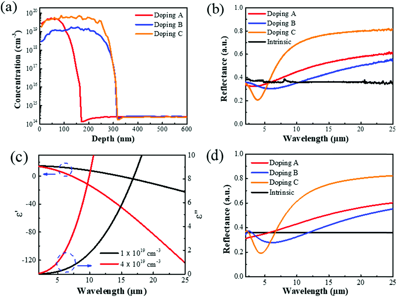 | ||
| Fig. 1 (a) n-type doping profiles of Doping A, B, and C. (b) Measured reflectance spectra of the intrinsic and doped Ge for Doping A, B, and C. (c) Calculated real (ε′) and imaginary part (ε′′) of Ge permittivity as a function of wavelength. The n-type doping profile with the doping concentration of 1 × 10¹⁹ and 4 × 1019 cm−3 were used for the calculation. (d) Simulated reflectance spectra of the intrinsic and doped Ge for Doping A, B, and C. The doping conditions for Doping A, Doping B, and Doping C are summarized in Table S1 (ESI†). | ||
Fig. 1(b) represents the reflectance spectra of the planar Ge samples. The reflectance spectrum of undoped planar Ge was measured to be 0.36 across the wavelength range measured. The reflectance spectra of the planar Ge with Doping A, B, and C were varied in the different wavelength regions. The reflectance near a wavelength of 3 μm dropped down to 0.21, while the reflectance in the wavelength range longer than 10 μm was higher than 0.40. The modulation of the reflectance spectra of the doped Ge is attributed to the changes in the permittivity of the Ge with different doping profiles because the doping profile can modulate the real (ε′) and imaginary part (ε′′)22 of Ge permittivity. The Drude model suffices to determine the permittivity. The Ge permittivity can be expressed by the following equations,32
 | (1) |
 | (2) |
 | (3) |
We introduce the inverted Ge pyramid texture to further reduce the reflectance in the wavelength range of 2 to 7 μm. It has been reported that the inverted pyramid texture displays a lower reflectance than the upright pyramid one.33 In addition, the surface area of the inverted pyramid structures is less than the upright pyramid structures, resulting in the low surface recombination loss.34Fig. 2(a) shows the schematic fabrication flow for the heavily doped inverted Ge pyramid array. The pristine undoped Ge samples were spin-coated with the photoresist and patterned by photolithography. Then, TiN was deposited on the photoresist-patterned surface via sputtering. The square TiN meshes with a square length of 4 μm and a spacing of 4 μm were obtained by the lift-off process. The MacEtch began in the open area where the Ge surface was exposed to etching solution.35 TiN meshes served as a catalyst in the MacEtch process.17 The schematic process mechanism of the MacEtch is shown in Fig. S5(a and b) (ESI†). The undercut was induced by longer etching, resulting in the larger inverted pyramid size.36 The additional etch time caused continuous inverse pyramid structures. The undercutting process is required to form continuous inverted Ge pyramids for low reflectance. The SEM image of the MacEtched inverted Ge pyramid with the undercut region is shown in Fig. S5(c) (ESI†). The width and height of the inverted pyramid were 6 and 5 μm, respectively. A core spectral window of reflectance and transmittance is demonstrated in the MIR range, resulting from the structure parameters of the inverted pyramid. Notably, the core spectral range can be adjusted towards a longer wavelength range by increasing the pyramid size.37 The angle between the straight sidewall and the wafer surface was 54.7°, which corresponds to the angle between (100) and (111) orientations. The ion implantation was performed on both the planar and textured Ge surfaces, followed by the KrF laser annealing process. The phosphorous (P) dopant dose was selected to be 1 × 10¹⁵ and 4 × 1015 cm−2. The laser fluence of 825 mJ cm−2 for 1 and 10 pulse irradiation was used for laser annealing. Fig. 2(b and c) show the top-view and cross-sectional scanning electron microscope (SEM) images of the inverted pyramid array, respectively.
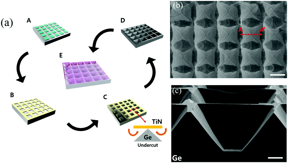 | ||
| Fig. 2 (a) Fabrication process flow of the heavily doped inverted Ge pyramid array: A. Ge sample (grey) with the patterned photoresist (green). B. Ge sample with TiN-patterned surfaces (yellow) after the lift-off process. C. The MacEtched inverted pyramid array. The undercut etching was conducted to form a continuous pyramid structure. D. TiN was delaminated by undercut etching of Ge. E. The surface of the inverted pyramid array was doped by ion implantation and subsequent laser annealing. (b) Top view SEM image of the inverted pyramid Ge array. The scale bar is 5 μm. (c) Cross-sectional SEM image of the inverted pyramid array along the dashed line A–A′ shown in (b). Scale bar is 2 μm. Note that the planar bottom region is due to sample cutting. | ||
Fig. 3 shows the reflectance and transmittance spectra of the inverted pyramid array made on both undoped and doped Ge. Simulated reflectance and transmittance spectra are also presented for comparison purposes. Fig. 3(a) shows the reflectance and transmittance spectra of the inverted undoped Ge pyramid. The reflectance spectrum of the planar Ge is included in the plot. The reflectance of the inverted Ge pyramid array was reduced in the broadband MIR range. Particularly, the reflectance was smaller than 0.10 when the wavelength was shorter than 7 μm. The reduction in the reflectance originates from the generation of lateral modes in the inverted pyramid array. Under normal illumination, the guided lateral mode is induced in the pyramid array. The induced lateral modes change the propagation path of the normal incident light, which results in the light scattering effect.27,36,38 The reflectance was continuously increased from 7 to 25 μm. Accordingly, the transmittance was 0.90 at 5 μm and it decreased to 0.70 at 25 μm. It is worth noting that the spectra of the inverted pyramid array follow the equation of 1 = R + T for intrinsic Ge because there is no absorption in this wavelength range, where R and T are the reflectance and the transmittance, respectively. The reflectance of the as-implanted inverted Ge pyramid array is shown in Fig. S2 (ESI†). No noticeable change was observed. Fig. 3(b–d) show the reflectance and transmittance spectra of the inverted Ge pyramid array with the doping profiles of Doping A, B, and C, respectively. The reflectance is consistent before and after the laser annealing process where the wavelength was smaller than 7 μm. However, the reflectance of three cases (i.e., Doping A, B, and C) continuously increased to 0.33, 0.45, and 0.55 at 15 μm. They kept increasing and reached 0.40, 0.55, and 0.62, respectively, at 25 μm. The increased reflectance of the laser-annealed Ge results from the recrystallization during the laser annealing process. Accordingly, the transmittance at 25 μm was reduced when the wavelength increased from 2 to 25 μm. The surface morphology after the laser annealing was investigated via the transmission electron microscopy (TEM) analysis as shown in Fig. S3(a–g) (ESI†). A thin amorphous Ge layer was observed with a thickness less than 10 nm from the center, sidewall, and edge of the inverted pyramid in Fig. S3(e–g) (ESI†), respectively. In addition, single crystallinity maintained in depth larger than 10 nm, indicating that the damaged Ge caused by the ion implantation was recrystallized after the laser annealing process. Fig. 3(c and d) represent the reflectance spectra of the inverted pyramid with the doping profile of Doping B and C, respectively. In comparison with Doping A, the reflectivity of the pyramid array with Doping C is enhanced to be 0.6 in the wavelength above 15 μm. The enhanced reflectance of Doping C results from a high doping concentration. The real permittivity decreases significantly when the doping concentration increases. The reflectance of the inverted pyramid array with Doping B displays 0.55 at 25 μm. The change in the reflectance between Doping B and C originates from the doping depth. Notably, the reflectance of the inverted pyramid array with Doping B is higher than the ones with Doping A although the doping depth is shallow. This implies that the doping depth is the dominant factor which determines the reflectance. Notably, no noticeable change in the reflectance is observed at 200, 250, and 300 K because Ge permittivity is consistent (Fig. S4 (ESI†)). It is also expected that the large incidence angle could result in high reflectance due to the high Fresnel coefficients.39
 | ||
| Fig. 3 Reflectance and transmittance spectra of the inverted pyramid array for (a) intrinsic and doped Ge with the doping profiles of (b) Doping A, (c) Doping B, and (d) Doping C obtained by FTIR and FDTD. The reflectance spectrum of the undoped planar Ge is displayed in (a) as the grey line for comparison purpose. The doping conditions for Doping A, Doping B, and Doping C are summarized in Table S1 (ESI†). | ||
It is important to investigate the variation in reflectance with different doping depth and concentration to optimize the doping profiles. Fig. 4(a and b) show the calculated reflectance and transmittance spectra of the inverted pyramid Ge array with the various doping profiles, respectively. The FDTD method was used to simulate the optical spectra in the wavelength range from 5 to 30 μm. The reflectance increased with doping concentration from intrinsic to 8 × 1019 cm−3 in the wavelength above 5 μm (Fig. 4(a)). The transmittance was decreased from 0.70 to nearly zero as shown in Fig. 4(b). In contrast, the transmittance was high in the wavelength range below 7 μm, which is comparable with the metal coatings on textured Si surfaces.21 However, the transmittance was reduced with increasing doping concentration in the short wavelength range. This is because heavily doped layers result in high absorption due to the enhanced extinction coefficient.22 The transmittance should be high enough in the core spectral window for high-efficiency antireflection. Thus, it should be required to choose the appropriate doping concentration to optimize the reflectance and transmittance. It should also be noted that doping depth can alter the reflectance and transmittance spectra of the pyramid array. The reflectance and transmittance spectra of the inverted pyramid Ge array can be adjusted by the doping depth as shown in Fig. 4(c) and (d), respectively. The doping concentration was selected to be 2 × 1019 cm−3 to study the effect of doping depth on the spectra. In Fig. 4(c), the reflectance was increased with the increasing doping depth in the wavelength range longer than 15 μm. Specifically, the reflectance was increased to 0.70 with the increasing doping depth up to 1000 nm, while the reflectance was maintained below 0.10 in the wavelength range smaller than 7 μm. In addition, the transmittance was decreased with the increasing doping depth (Fig. 4(d)). The transmittance was smaller than 0.10 in the wavelength range longer than 15 μm, while the transmittance was larger than 0.70 in the wavelength range shorter than 7 μm. The absorption coefficient increases with increasing doping concentration in the MIR range due to the plasmonic behavior.22 Therefore, the enhanced absorption reduces the transmittance in the calculated wavelength range.
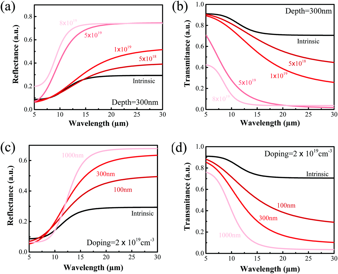 | ||
| Fig. 4 (a) Simulated reflectance and (b) transmittance spectra of the heavily doped inverted Ge pyramid array with different doping concentrations. The doping depth is fixed to be 300 nm. (c) Simulated reflectance and (d) transmittance spectra of the inverted Ge pyramid array with different doping depths. The doping concentration is fixed to be 2 × 1019 cm−3. The reflectance and transmittance spectra are obtained by the FDTD simulation. | ||
Conclusions
In conclusion, we have demonstrated an inverted Ge pyramid array combined with n-doping with various doping profiles for tunable antireflection in the MIR range. The inverted pyramid array and high doping concentrations are realized by the MacEtch and KrF laser annealing process, respectively. The inverted pyramid texture serves as the effective antireflective structure in the broad MIR wavelength range. In addition, the heavy doping profiles result in high reflectance due to the modulated permittivity of Ge. We also find that the reflectance and transmittance can be further modulated by the doping concentration and doping depth. It should be noted that the high reflectance higher than 0.60 is achieved in heavily doped pyramid structures with a doping concentration of 4 × 1019 cm−3. It has an increase in reflectance approximately two times that of the intrinsic one. The effect of doping profiles (i.e., doping concentration and depth) on the reflectance and transmittance is thoroughly analyzed by the FDTD simulation. Our results provide a robust and viable method to tune the reflectance and transmittance for advanced CMOS compatible MIR photonic and optoelectronic applications.Experimental section
Formation of a Ge inverted pyramid array by MacEtch
Undoped Ge wafers were cleaned using acetone, isopropyl alcohol (IPA), and deionized (DI) water. The prebaked Ge pieces were spin-coated with a photoresist (AZ-5214) and patterned by photolithography. Subsequently, TiN was deposited on the photoresist-patterned surfaces via sputtering. The lift-off process was conducted in the acetone solution. The square TiN meshes with a square length of 4 μm and the space of 4 μm were obtained. An etching mixture consisting of potassium permanganate (KMnO4) (1.27 mM) and DI water (15.82 mM) was used for the MacEtch process at 60 °C for 120 min.Formation of heavy doping profiles
Phosphorus (P) ion implantation was performed at 25 keV for n-type doping at room temperature. The ion implantation dose was selected to be 1 × 10¹⁵ and 4 × 1015 cm−2. The ion beam was tilted with 7° to the normal to the wafer surface. After the ion implantation, a KrF excimer laser was implemented for the dopant activation. A Roaster mode with a single spot size of 200 × 200 μm2 was used. The laser fluence was selected to be 825 mJ cm−2. The n-type profile for Doping A was obtained with 4 × 1015 cm−2 for single pulse irradiation. The doping profiles for Doping B and C were obtained with the dopant dose of 1 × 10¹⁵ and 4 × 1015 cm−2 for 10 pulses irradiation, respectively.Finite-difference time-domain (FDTD) simulation
The real and imaginary parts of permittivity of Ge were obtained from ref. 20 and 28. A plane-wave light source was selected for normal incident illumination. A perfectly matched layer (PML) was used in the z-axis. The reflectance and transmittance monitors were positioned at the back side of the light source and at the Ge depth of 10 μm, respectively. The simulation window was applied in 6 μm × 6 μm in the x–y plane and 20 μm in the z direction.Characterization of the heavily doped Ge pyramid structure
Top and cross-sectional images of the inverted Ge pyramid array were taken using a field emission scanning electron microscope (FESEM, Sirion, FEI Netherlands). SRP was conducted to obtain the doping concentration of the planar Ge samples. The SRP method was performed in a 100 × 100 μm2 area to obtain the activated doping concentration. The Bevel angle was 0.00192° with the step increment of 2 μm. The probe load was calibrated to be 2.6 g. The reflectance spectra were obtained using a Vertex 70v FTIR spectrometer in the wavelength range from 2 to 25 μm.Data availability statement
The data that support the findings of this study are available from the corresponding author upon reasonable request.Conflicts of interest
The authors declare no conflict of interest.Acknowledgements
This work was supported by the National Research Foundation, Singapore, under its Competitive Research Program (CRP Award NRF-CRP19-2017-01), A*STAR Programmatic Funds (A18A7b0058), AME IRG and YIRG grants (A20E5c0095 and A2084c0066), Ministry of Education AcRF Tier 1 (2021-T1-002-031 (RG112/21)), Ministry of Education AcRF Tier 2 (T2EP50120-0003 and T2EP50121-0001 (MOE-00180-01)), and the Nanyang Technological University (NTU) start-up grant (M4082289.040). The authors acknowledge the support of the Nanyang NanoFabrication Centre (N2FC).References
- R. Dickie, R. Cahill, V. Fusco, H. S. Gamble and N. Mitchell, THz Frequency Selective Surface Filters for Earth Observation Remote Sensing Instruments, IEEE Trans. Terahertz Sci. Technol., 2011, 1(2), 450–461 Search PubMed.
- A. K. Rashid and Q. Zhang, “A Low-Cost Terahertz Frequency Selective Structure”, 2020 IEEE International Conference on Computational Electromagnetics (ICCEM), (2020) DOI:10.1109/ICCEM47450.2020.9219339.
- H. D. Liu, B. Yang, M. R. Mao, Y. Liu, Y. M. Chen, Y. Cai, D. J. Fu, F. Ren, Q. Wan and X. J. Hu, Enhanced thermal stability of solar selective absorber based on nano-multilayered TiAlON films deposited by cathodic arc evaporation, Appl. Surf. Sci., 2020, 501, 144025 CrossRef CAS.
- A. A. Bushunov, M. K. Tarabrin and V. A. Lazarev, Review of Surface Modification Technologies for Mid-Infrared Antireflection Microstructures Fabrication, Laser Photonics Rev., 2021, 15(5), 2000202 CrossRef CAS.
- S. S. K. Poushi, H. Mahmoudi, M. hofbauer, B. Steindl and H. Zimmermann, Photon detection probability enhancement using an antireflection coating in CMOS-based SPADs, Appl. Opt., 2021, 60(25), 7815–7820 CrossRef PubMed.
- A. Dan, H. C. Barshilia, K. Chattopadhyay and B. Basu, Solar energy absorption mediated by surface plasma polaritons in spectrally selective dielectric-metal-dielectric coatings: A critical review, Renewable Sustainable Energy Rev., 2017, 79, 1050–1077 CrossRef.
- K. Xu, M. Du, L. Hao, J. Mi, Q. Yu and S. Li, A review of high-temperature selective absorbing coatings for solar thermal applications, J. Materiom., 2020, 6, 167–182 CrossRef.
- H. D. Liu, T. R. Fu, M. H. Duan, Q. Wan, C. Luo, Y. M. Chen, D. J. Fu, F. Ren, Q. Y. Li, X. D. Cheng, B. Yang and X. J. Hu, Structure and thermal stability of spectrally selective absorber based on AlCrON coating for solar-thermal conversion applications, Sol. Energy Mater. Sol. Cells, 2016, 157, 108–116 CrossRef CAS.
- F. Cao, D. Kraemer, L. Tang, Y. Li, A. P. Litvinchuk, J. Bao, G. Chen and Z. Ren, A high-performance spectrally-selective solar absorber based on a yttria-stabilized zirconia cermet with high-temperature stability, Energy Environ. Sci., 2015, 10, 3040–3048 RSC.
- X. Liu, P. R. Coxon, M. Peters, B. Hoex, J. M. Cole and D. J. Fray, Black silicon: fabrication methods, properties and solar energy applications, Energy Environ. Sci., 2014, 7, 3223–3263 RSC.
- T. P. Pasanen, J. Isometsä, M. Garin, K. Chen, V. Vähänissi and H. Savin, Nanstructured Germanium with >99% Absorption at 300–1600 nm Wavelengths, Adv. Opt. Mater., 2020, 8, 2000047 CrossRef CAS.
- T. Kawase, A. Mura, K. Dei, K. Nishitani, K. Kawai, J. Uchikoshi, M. Morita and K. Arima, Metal-assisted chemical etching of Ge(100) surfaces in water toward nanoscale patterning, Nanoscale Res. Lett., 2013, 8, 151 CrossRef PubMed.
- Z.-J. Zhao, S.-H. Shin, S. Y. Lee, B. Son, Y. Liao, S. Hwang, S. Jeon, H. Kang, M. Kim and J.-H. Jeong, Direct Chemisorption-Assisted Nanotransfer Printing with Wafer-Scale Uniformity and Controllability, ACS Nano, 2022, 16, 378–385 CrossRef CAS PubMed.
- S. An, Y. Liao, S. Shin and M. Kim, Black Germanium Photodetector Exceeds External Quantum Efficiency of 160%, Adv. Mater. Technol., 2021, 2100912 Search PubMed.
- B. Son, H. Zhou, Y. Lin, K. H. Lee and C. S. Tan, Gourd-shaped hole array germanium (Ge)-on-insulator photodiodes with improved responsivity and specific detectivity at 1,550 nm, Opt. Express, 2021, 29(11), 16520–16533 CrossRef CAS PubMed.
- Y. Nishijima, R. Komatsu, S. Ota, G. Seniutinas, A. Balčytis and S. Juodkazis, Anti-reflective surfaces: Cascading nano-microstructuring, APL Photonics, 2016, 1, 076104 CrossRef.
- Y. Liao, S. H. Shin, Y. Jin, Q. J. Wang and M. Kim, Producing Microscale Ge Textures via Titanium Nitride- and Kickel-Assisted Chemical Etching with CMOS-Compatibility, Adv. Mater. Interfaces, 2021, 8, 2100937 CrossRef CAS.
- L. Yang, L. Mo, T. Chen, E. Forsberg and S. He, A checkerboard selective absorber with excellent spectral selectivity, J. Appl. Phys., 2015, 118, 183103 CrossRef.
- B. Zhang, J. Hendrickson, N. Nader, H.-T. Chen and J. Guo, Metasurface optical antireflection coating, Appl. Phys. Lett., 2014, 105, 241113 CrossRef.
- W. Streyer, K. Feng, Y. Zhong, A. J. Hoffman and D. Wasserman, Selective absorbers and thermal emitters for far-infrared wavelengths, Appl. Phys. Lett., 2015, 107, 081105 CrossRef.
- L. Huang, C.-C. Chang, B. Zeng, J. Nogan, S.-N. Luo, A. J. Taylor, A. K. Azad and H.-T. Chen, Bilayer Metasurfaces for Dual- and Broadband Optical Antireflection, ACS Photonics, 2017, 4, 2111–2116 CrossRef CAS.
- J. Frigerio, A. Ballabio, G. Isella, E. Sakat, G. Pellegrini, P. Biagioni, M. Bollani, E. Napolitani, C. Maganelli, M. Virgilio, A. Grupp, M. P. Fischer, D. Brida, K. Gallacher and D. J. Paul, Tunability of the dielectric function of heavily doped germanium thin films for mid-infrared plasmonics, Phys. Rev. B: Condens. Matter Mater. Phys., 2016, 94, 085202 CrossRef.
- L. Baldassarre, E. Sakat, J. Frigerio, A. Samarelli, K. Gallacher, E. Calandrini, G. Lsella, D. J. Paul, M. Ortolani and P. Biagioni, Midinfrared Plasmon-Enhanced Spectroscopy with Germanium Antennas on Silicon Substrates, Nano Lett., 2015, 15, 7225–7231 CrossRef CAS PubMed.
- H. Chong, Z. Xu, Z. Wang, J. Yu, T. Biesner, M. Dressel, L. Wu, Q. Li and H. Ye, CMOS-Compatible Antimony-Doped Germanium Epilayers for Mid-Infrared Low-Loss High-Plasma-Frequency Plasmonics, ACS Appl. Mater. Interfaces, 2019, 11, 19647–19653 CrossRef CAS PubMed.
- G. Pellegrini, L. Baldassare, V. Giliberti, J. Frigerio, K. Gallacher, D. J. Paul, G. Isella, M. Ortolani and P. Biagioni, Benchmarking the Use of Heavily Doped Ge for Plamonics and Sensing in the Mid-Infrared, ACS Photonics, 2018, 5, 3601–3607 CrossRef CAS.
- Z. Wang, H. Chong, J. Yang and H. Ye, Study on epsilon crossover wavelength tuning of heavily doped germanium-on-silicon in mid-infrared range, Opt. Express, 2019, 27(23), 33724–33736 CrossRef CAS PubMed.
- R. Milazzo, G. Impellizzeri, D. Piccinotti, A. La Magna, G. Fortunato, D. De Salvador, A. Carnera, A. Portavoce, D. Mangelinck, V. Privitera and E. Napolitani, Impurity and defect interfactions during laser thermal annealing in Ge, J. Appl. Phys., 2016, 119, 045702 CrossRef.
- G. Impellizzeri, E. Napolitani, S. Boninelli, G. Fisicaro, M. Cuscunà, R. Milazzo, A. La Magna, G. Fortunato, F. Priolo and V. Privitera, B-doping in Ge by excimer laser annealing, J. Appl. Phys., 2013, 113, 113505 CrossRef.
- R. Milazzo, E. Napolitani, G. Impellizzeri, G. Fisicaro, S. Boninelli, M. Cuscunà, D. De Salvador, M. Mastromatteo, M. Italia, A. La Magna, G. Fortunato, F. Priolo, V. Privitera and A. Carnera, N-type doping of Ge by As implantation and excimer laser annealing, J. Appl. Phys., 2014, 115, 053501 CrossRef.
- J. H. Parker, Jr., D. W. Feldman and M. Ashkin, Raman Scattering by Silicon and Germanium, Phys. Rev., 1967, 155, 712 CrossRef.
- J. Biswas, N. Pradhan, D. Biswas and S. Das, Impact of Punch-through Stop Implants on Channel Doping and Junction Leakage for Ge p-FinFET Applications, IEEE Trans. Electron Devices, 2019, 66(4), 1635–1641 CAS.
- R. Soref, J. Hendrickson and J. W. Cleary, Mid- to ling-wavelength infrared plasmonic-photonics using heavily doped n-Ge/Ge and n-GeSn/GeSn heterostructures, Opt. Express, 2012, 20(4), 3814–3824 CrossRef CAS PubMed.
- D. Zhang, S. Jiang, K. Tao, R. Jia, H. Ge, X. Li, B. Wang, M. Li, Z. Ji, Z. Gao and Z. Jin, Fabrication of inverted pyramid structure for high-efficiency silicon solar cells using metal assisted chemical etching method with CuSO4 etchant, Sol. Energy Mater. Sol. Cells, 2021, 230, 11200 Search PubMed.
- M. K. Basher, M. K. Hossain and M. A. R. Akand, Effect of surface texturization on minority carrier lifetime and photovoltaic performance of monocrystalline silicon solar cell, Optik, 2019, 176, 93–101 CrossRef CAS.
- M. Kim, S. Yi, J. D. Kim, X. Yin, J. Li, J. Bong, D. Liu, S.-C. Liu, A. Kvit, W. Zhou, X. Wang, Z. Yu, Z. Ma and X. Li, Enhanced Performance of Ge Photodiodes via Monolithic Antireflection Texturing and α-Ge Self-Passivation by Inverse Metal-Assisted Chemical Etching, ACS Nano, 2018, 12, 6748–6755 CrossRef CAS PubMed.
- S.-H. Shin, Y. Liao, B. Son, Z.-J. Zhao, J.-H. Jeong, C. S. Tan and M. Kim, A highly ordered and damage-free Ge inverted pyramid array structure for broadband antireflection in the mid-infrared, J. Mater. Chem. C, 2021, 9, 9884–9891 RSC.
- Y. W. Chen, P. Y. Han and X.-C. Zhang, Tunable broadband antireflection structures for silicon at terahertz frequency, Appl. Phys. Lett., 2009, 94, 041106 CrossRef.
- Y. Nishijima, R. Komatsu and S. Ota, Anti-reflective surface: Cascading nano-/microstructuring, APL Photonics, 2016, 1, 076103 CrossRef.
- V. Magnin, J. Harari, M. Halbwax, S. Bastide, D. Cherfi and J.-P. Vilcot, Angle-dependent ray tracing simulations of reflections on pyramidal textures for silicon solar cells, Sol. Energy, 2014, 110, 378–385 CrossRef CAS.
Footnotes |
| † Electronic supplementary information (ESI) available. See DOI: 10.1039/d2tc00141a |
| ‡ These authors contributed equally to this work. |
| This journal is © The Royal Society of Chemistry 2022 |