
 Open Access Article
 This Open Access Article is licensed under a
 Creative Commons Attribution 3.0 Unported Licence
Unit cell distortion and surface morphology diversification in a SnTe/CdTe(001) topological crystalline insulator heterostructure: influence of defect azimuthal distribution†
Adrian
Sulich
 *a,
Elżbieta
Łusakowska
a,
Wojciech
Wołkanowicz
a,
Piotr
Dziawa
a,
Janusz
Sadowski
ab,
Badri
Taliashvili
a,
Tomasz
Wojtowicz
c,
Tomasz
Story
ac and
Jaroslaw Z.
Domagala
a
*a,
Elżbieta
Łusakowska
a,
Wojciech
Wołkanowicz
a,
Piotr
Dziawa
a,
Janusz
Sadowski
ab,
Badri
Taliashvili
a,
Tomasz
Wojtowicz
c,
Tomasz
Story
ac and
Jaroslaw Z.
Domagala
a
aInstitute of Physics, Polish Academy of Sciences, Aleja Lotnikow 32/46, PL 02 668 Warsaw, Poland. E-mail: sulich@ifpan.edu.pl
bDepartment of Physics and Electrical Engineering, Linnaeus University, 391 82 Kalmar, Sweden
cInternational Research Centre MagTop, Institute of Physics, Polish Academy of Sciences, Aleja Lotnikow 32/46, PL 02 668 Warsaw, Poland
First published on 5th January 2022
Abstract
Challenges and opportunities arising from molecular beam epitaxial growth of topological crystalline insulator heterostructures composed of a rock-salt SnTe(001) layer of varying thickness (from 80 nm to 1000 nm) and a zinc blende 4 μm thick CdTe(001) buffer layer grown on a commercial GaAs(001) substrate with 2° off-cut toward the [100] direction were studied with a focus on crystal lattice strain, unit cell symmetry breaking and surface quality. The results indicate that the CdTe buffer is almost fully relaxed whereas in SnTe layers slight anisotropic relaxation is observed that varies from 86.2% to 98.3% with the layer thickness increasing. The relaxation process involves formation of misfit dislocations, mainly of Lomer-type (consisting of two associated 60° dislocations), both at CdTe/GaAs and SnTe/CdTe interfaces. Azimuthal spatial distribution of defects is anisotropic due to a disparity of 60° dislocation mobility toward orthogonal [−110] and [110] crystallographic directions. This results in a monoclinic distortion of the SnTe unit cell, as observed especially in the layers grown without additional Te molecular flux. A reflections selection method is proposed to measure such crystal deformations. Qualitatively new morphology of the SnTe surface of a reduced symmetry with nanoripple-like structures oriented close to the 〈100〉 (or, rarely, to 〈120〉) crystallographic in-plane direction is observed. The possible mechanism of their formation is dislocation-driven while their extended shape and predominant crystalline orientation may be influenced by the anisotropy of defect azimuthal distribution. Due to the magnitude of measured lattice strain (∼10−3) the monoclinic distortion in SnTe(001) layers is expected to be large enough to affect their physical properties, e.g., offering the way of controlling the crystal-symmetry-protected surface states (deformation-induced opening of the energy gap in the spectrum of metallic topological surface states). Thus, it may serve as an additional degree of freedom in designing topological spintronic devices.
Introduction
Tin telluride (SnTe) is a IV–VI narrow-gap semiconductor well known for infrared optoelectronic and thermoelectric applications, with SnTe/PbTe substitutional alloys being constituent materials of modern thermoelectric generators designed for use in the mid-temperature range.1 A recent breakthrough discovery of the topological crystalline insulator (TCI) properties of SnTe-based IV–VI alloys2–14 has brought to light a new exciting and useful feature of this class of materials. It is related to an expected almost dissipation-free electron transport mechanism via topological surface or edge states, with great technological potential in novel low-power-consumption electronic devices.15The topological properties of a crystalline material, also fulfilling other indispensable criteria, such as electronic band inversion in given points of a Brillouin zone and strong spin orbit coupling, are governed by symmetry. In SnTe rock-salt cubic crystals the topological states exist on specific crystal facets, including important highest symmetry surfaces {100}, {110}, and {111}, with a key topological role of {110} mirror-plane symmetry.3–14 Any symmetry breaking mechanism will inevitably affect these properties. In the specific case of SnTe it is largely known both from theoretical modelling16,17 and from experiment.18 Theoretical analysis of the influence of crystal lattice distortions of various symmetries is shown, e.g. in the seminal paper by M. Serbyn and L. Fu.19 There have also been experimental observations of distortion-induced opening of the gap in metallic topological surface states – all important for the electrical and infrared optoelectronic properties of SnTe and SnSe-based materials.8,9,20
Further progress of this field, nowadays based mostly on bulk materials, critically needs development of functional multilayer heterostructures deposited on a proper commercially available substrate. In particular, investigation of the molecular beam epitaxial (MBE) growth of SnTe on GaAs – a commonly used substrate for many semiconductors – is highly desirable, since the substrates for epitaxy matched to SnTe (with the lattice parameter close to 6.3 Å) are scarce and/or very expensive (e.g. InSb). Our work vitally contributes to solving this important application problem by analysis of SnTe/CdTe heterostructure growth.
SnTe, CdTe and GaAs are semiconductor materials that have been known for a long time and extensively investigated in various aspects (see for example ref. 21–51); their basic structural parameters (crystal structure, lattice parameter a0 and coefficient of linear thermal expansion α) are listed in Table 1. However, papers devoted to the crystallographic study of SnTe(001) layers grown on GaAs with a CdTe(001) buffer, as well as of CdTe(001) layers on GaAs, are not very abundant to our knowledge.47–51 Thus detailed investigations of such heterostructures are potentially useful for further technological development of both already well-established fields of layered thermoelectrics and infrared detectors as well as in new fields of electric and optical topological heterostructures.
| Compound | Crystal structure | a 0 (Å) | Type of data | Ref. | α (10−6 1/K) | Ref. |
|---|---|---|---|---|---|---|
| a Measurements were performed at room temperature (293 K–298 K) and at atmospheric pressure. | ||||||
| GaAs | Zinc blende | 5.65321(3) | Powder diffractiona | 52 | 5.73 | 53 |
| CdTe | Zinc blende | 6.4827 | Single-crystal diffractiona | 54 | 6.0 | 55 |
| 4.8 | 49 | |||||
| ZnTe | Zinc blende | 6.106(1) | Single-crystal diffractiona | 56 | 8.4 | 57 |
| SnTe | Rock salt | 6.3198 | Single-crystal diffractiona | 8 | 20 | 55 |
The aim of our research is to perform a comprehensive structural analysis of SnTe(001) epitaxially grown on CdTe(001)/GaAs over a broad, practically relevant, range of SnTe layer thickness, strain, stoichiometry, and growth regimes with evaluation of the crystallographic quality of the samples, lattice strain, unit cell symmetry and size, epitaxial relation of misorientation of the respective layers, distribution of defects, and surface morphology. Such analysis helps to recognize the challenges and opportunities arising upon MBE growth of SnTe thin crystalline films on GaAs substrates, especially with respect to the control of the unit cell deformation, determined by lattice or thermal mismatch, as well as surface morphology.
We show this experimentally and propose a model explaining the origin of the intriguing epitaxial relation observed between the semiconductor layers in the (001)-oriented SnTe/CdTe/GaAs heterostructure, involving a crystal structure (zinc blende GaAs and CdTe vs. rock-salt SnTe) and lattice parameter Δa/a = 2.5% SnTe-CdTe mismatch. Due to formation of a distinct dislocations network one observes a reduction in the expected four-fold crystal symmetry of the SnTe layer with formation of a monoclinic unit cell and with broadening of the linear ripple-type structures present on its surface in comparison with the tetragonal one. In the case of breaking the (110) mirror plane symmetry, opening of the gap in the Dirac-cone-type electron spectrum of topological TCI surface states is expected – the important effect for developing new electronic or far infrared optoelectronic devices.
Preparation of samples
Each heterostructure was grown using two separate molecular beam epitaxial setups (for the growth of II–VI and IV–VI semiconductors, respectively). The successful procedure developed by us involves the growth of a Te-capped CdTe/GaAs compliant substrate, followed by the transfer to the IV–VI MBE growth chamber, thermal decapping of Te (controlled in situ by reflection high energy electron diffraction – RHEED) and subsequent growth of the SnTe layer.During the first stage a 4 μm thick CdTe buffer layer is grown on the GaAs(001) substrate with a 2° off-cut toward the [100] direction, see Fig. 1. The same kind of CdTe buffer was earlier used by us for the growth of closely related PbTe/CdTe heterostructures.58 The lattice parameter of rock-salt PbTe is equal to 6.46 Å, i.e. it is almost lattice matched to CdTe (6.48 Å). This GaAs substrate has a surface composed of terraces with A-type and B-type steps.59,60 The A-type steps occur along the [1−10] direction and have smooth edges. The B-type step edges are oriented toward [110] and are much rougher with numerous kink-sites which during the layer growth increase the nucleation rate.61 Geometrical estimation for the 2° off-cut (001) surface results in a terrace width of around 40 Å. However, their accurate value is unknown due to GaAs surface reconstruction (variously arranged As dimers) depending on many factors, e.g., off-cut direction and temperature. The values of terrace width known from the literature for GaAs(001) with 2° off-cut along the [110] direction are in the range of 50 Å–120 Å.62 The 2° off-cut toward the [100] direction reduces the problem of CdTe twinning and enables the growth of a high quality epitaxial film.59 CdTe can grow on GaAs(001) with two possible crystal directions, [001] or [111]. To enhance the occurrence of the former, an additional very thin (ca. 7 nm) ZnTe layer is first deposited on GaAs(001).63 ZnTe is known to suppress the growth of the CdTe layer with (111) orientation by biasing the Stransky–Krastanov growth mode.64 The ZnTe/GaAs mismatch is smaller than the CdTe/GaAs one: 8% and 14.7%, respectively.65
 | ||
| Fig. 1 Scheme of the substrate and buffer layer structures: (a) GaAs terraces and off-cut (the width of the terrace is about 30 times the height of the step); (b) azimuthal twist of CdTe terraces in reference to the direction of GaAs terraces; (c) tilt of the (100) planes in the CdTe lattice in reference to the same planes in the GaAs lattice (the SnTe (001) planes nearly parallel to the (001) CdTe planes). | ||
At the second stage, just before transferring the sample into another MBE system, tellurium oxides were etched using bromomethanol (0.5% of Br2).
The remaining amorphous tellurium coating was desorbed in the MBE growth chamber at a temperature T ≈ 250 °C–300 °C. The recovered surface revealed a clear streaky RHEED pattern corresponding to the atomically smooth surface of the monocrystalline CdTe buffer layer. Subsequently this layer was refreshed by deposition of 50 nm thick CdTe. Next the SnTe layer with a thickness in the range of 20 nm to 1000 nm was grown at 310 °C with a beam equivalent pressure of SnTe molecular flux around (4.75 ± 0.85) × 10−7 mbar. Only in the case of two samples was the growth temperature different, 370 °C and 270 °C. For all the samples the regime of small Te excess corresponding to the thermodynamically expected non-stoichiometry in SnTe was fulfilled. According to the phase diagrams presented in ref. 66 and 67, the homogeneity region of the Sn–Te system covers a composition of Sn1−xTe where x is in the range from 0.004 to 0.035. To check the influence of deviation from stoichiometry we used two sources – SnTe and Te. Various Te/SnTe molecular beam flux ratios, in the range from 0 to 0.0156 were applied.
Experimental techniques
Assessment of the samples’ crystallographic quality and the measurements of lattice strain, layer misorientation and defect distribution were carried out using a high-resolution X-ray diffraction (HR XRD) technique. We apply a Philips X'Pert MRD diffractometer with CuKα1 radiation (λ = 1.5406 Å), equipped with: an X-ray mirror (forming the primary divergent beam to quasi-parallel), four-fold bounce, an asymmetrically cut Ge(220) monochromator in the incident beam path and an arm with two proportional detectors in the reflected beam path. One of the detectors is fully opened (in the so-called double-axis configuration) and the second is preceded by the three-bounce Ge(220) analyzer crystal (triple-axis configuration). The divergence of an output beam in the horizontal plane is equal to 21 arcseconds (′′). A set of performed measurements and a research methodology applied to their interpretation is described in detail in the ESI.†The surface morphology of the samples was studied using a Bruker Dimension Icon Atomic Force Microscope (AFM). The measurements were performed in the tapping mode, which is the safest for the measured surface. In the tapping mode measurements are carried out by tapping the surface with the oscillating tip. This eliminates shear forces which can damage soft samples and reduce image resolution. Lateral resolution on most samples in this operating mode is from 1 nm to 5 nm. We have used the silicon probes model OTESPA with a nominal tip radius of curvature from 5 nm to 10 nm. The probed areas are: 2 × 2 μm, 6 × 6 μm, 10 × 10 μm, and 50 × 50 μm. We used the Section and Roughness functions to analyse the images. Depth, height, width, and angular measurements were performed with the Section function. The Root Mean Square (RMS) parameter was applied for the roughness analysis.
Results and discussion
General crystallographic quality of the samples
The preliminary measurements show that the mean full width at half maximum values of rocking curves (RC FWHM) for 004 reflections coming from the individual layers in the samples are: 300” for CdTe (the lowest measured value: 205′′ and the highest: 535′′) and 889′′ for SnTe (the lowest value: 468′′ and the highest: 2427′′). Thus, the mean values are comparable with the reported data.63,68,69 The individual FWHM values for SnTe depend significantly on the layer thickness (see Fig. 2).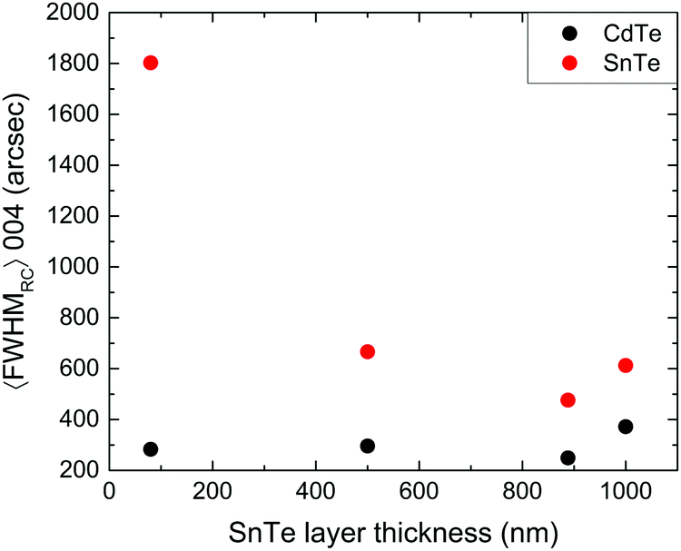 | ||
| Fig. 2 Rocking curve's FWHM of 004 reflections for CdTe and SnTe layers in the investigated samples. The results were twice averaged: for two perpendicular directions: [110] and [−110] and, afterward, for the groups of samples with respective SnTe layer thicknesses. | ||
The highest values (above 1000′′) measured for the 80 nm SnTe samples should be attributed to the slightly higher concentration of defects rather than to the small layer thickness. The contribution of a small layer thickness to the increase of the symmetrical 004 RC FWHM value can be estimated as ∼200′′ (by a simulation of RC from an ideal 80 nm SnTe layer). In the case of the thinnest SnTe layer (20 nm) the RC measurement was not possible because of the too low signal intensity. Therefore, the sample is investigated only with AFM. The quality of the samples does not correlate with the Te/SnTe molecular beam flux ratio in the studied range. Likewise, there is no significant difference in the defect concentrations in the CdTe and SnTe layers between the directions horizontal and vertical to the sample surface, which is denoted by the fact that the analysis of the RC FWHM of asymmetrical reflections (−1−15 for CdTe and −2−26 for SnTe) supplied similar results to those obtained for the 004 reflections.
XRD examination confirmed that in accordance with the producer's specification the GaAs substrate off-cut is approximately the same (2 ± 0.06°) and it is directed towards the same crystallographic direction [100] denoted by the comparable values of GaAs off-cut azimuthal angle ∼41° with the lowest measured value 37° and the highest 44°, obtained at the same sample alignment during the measurement and with the error limits estimated to be ±4°. In the set of investigated samples we found distinct CdTe/GaAs (001) crystallographic plane misorientation (tilt) up to 0.8°. For the sake of clarity, we note that the crystallographic directions lying on the (001) plane in both the substrate and the buffer are parallel. At the same time we observe that the CdTe surface “drops” not along the GaAs off-cut direction [100] but is twisted up to 23°, see Fig. 3a and b. We name it the azimuthal angle twist. The average values of CdTe/GaAs plane misorientation (tilt) and its azimuthal angle change for the groups of samples with particular SnTe thickness are up to 0.6° and up to 18°, respectively. As it was established, the tilt is created by a network of misfit dislocations70 and is proportional to the lattice mismatch between the substrate and the layer.71 Thus, this kind of network must be present in our samples. Moreover, the mechanism of the generation of the tilt in layers deposited on vicinal substrates is based on the strain relaxation asymmetry consisting of predominant emergence of misfit dislocations with the opposite “out-of-plane” component of the Burgers vector.72
 | ||
| Fig. 3 Influence of SnTe layer thickness on: (a) the relative layers’ plane misorientation (α) of CdTe/GaAs and SnTe/CdTe; (b) the relative layers’ plane misorientation azimuthal angle change (Δφ). | ||
The differences in CdTe/GaAs plane misorientation and its azimuthal angle change in the individual samples are charted in Fig. 3. The range of the results diversification shows that the individual pieces of used CdTe/GaAs substrate are not identical, despite the fact they were made in the same laboratory. SnTe/CdTe plane misorientation and its azimuthal angle variation are significantly smaller than those for CdTe/GaAs. The misorientation is up to 0.12° (average values for particular groups with the same SnTe thickness: up to 0.08°) and the azimuthal angle change is up to 2° (average values: up to 1°). These smaller values can be explained by a smaller mismatch between SnTe and CdTe than in the case of CdTe and GaAs. They are also consistent with previous observations indicating that the tilt is inversely proportional to the preliminary defect density,72 which must be higher in SnTe. Besides that, it can be reduced by reactions between dislocations.72
Strain relaxation degree in the CdTe buffer and SnTe layer
The investigated samples have “in-plane” lattice parameters a‖ of CdTe buffer in the range of 6.471–6.485 (±0.003) Å with 〈a‖〉 = 6.481 (±0.003) Å and “out-of-plane” lattice parameters a⊥ in the range of 6.4852–6.4864 (±0.0002) Å with 〈a⊥〉 = 6.4855 (±0.0002) Å. The measurement uncertainty for the “out-of-plane” lattice parameter amounts to ±0.0002 Å and for the “in-plane” ±0.003 Å for both the CdTe buffer and SnTe layers.As known from the literature, the bulk lattice parameter value of cubic CdTe is equal to 6.4827(8).54 Thus, in the samples a small tetragonal distortion of the CdTe unit cell occurs and has an in-plane compressive nature, due to a‖ < a⊥. The differences in a‖ values measured at different azimuthal angles (φ) (reflection −115 and −1−15) do not exceed a measurement uncertainty ±0.003 Å, therefore a deformation of the order higher than the tetragonal one does not occur.
An exception is one of the two samples grown with an 80 nm SnTe layer and at the Te/SnTe molecular flux ratio equal to 0, for which the azimuthal difference of a‖ amounts to 0.012 Å which may indicate the presence of a monoclinic deformation. Similarly, the differences of a⊥ are also not bigger than the measurement uncertainty range (in this case ±0.0002 Å), except for the same sample, with a difference of a⊥ equal to 0.00095 Å. Thus, the buffer layer in this sample is less standard than in the other ones.
The tetragonal distortion detected in SnTe is tensile (due to a‖ > a⊥), distinctly larger than in CdTe and largest for the samples with the thinnest layer, see Fig. 4a. It has also been ascertained that in some samples, mainly grown at the molecular flux ratio Te/SnTe = 0, a⊥ values calculated from the tetragonal crystal unit depend on the azimuthal angle and the differences between them are significantly bigger than the measurement uncertainty (0.003 Å), see Fig. 4b.
 | ||
| Fig. 4 (a) Influence of SnTe layer thickness on lattice parameters in SnTe; the calculations were done using the tetragonal or monoclinic unit cell model (appropriate for the detected distortion) and the results were twice averaged: for two perpendicular directions: [110] and [−110] and, afterward, for the groups of samples with respective SnTe layer thicknesses. (b) Differences of “in-plane” lattice parameters in SnTe, calculated using the tetragonal unit cell model; the red line depicts the value of measurement uncertainty (0.003 Å). The points above the red line clearly show that the tetragonal model is not appropriate for the samples indicated. | ||
This suggests the presence of monoclinic deformation of the SnTe unit cell; a similar type of deformation was earlier reported for GexSi1−x layers grown on vicinal Si(001).73 A unit cell deformation to a lower than orthorhombic symmetry order was also found in partially relaxed InGaAs/InxAl1−xAs/InP (the structure was rhomboidal, since for the zinc blende unit cell the monoclinic deformation is unlikely);74 and in strained, hexagonal InGaN, deposited on off-cut GaN (00.1) (in this case the structure was triclinic).75 It is possible that some kind of angular deformation of the unit cell occurred also in mismatched heterostructures of InGaAs/GaAs76 and InP/InAlAs/InGaAs,77 however, the results referred to in these papers were interpreted differently (orthorhombic symmetry was assumed).
As is well-known, the typical value of the bulk, cubic SnTe lattice parameter is 6.315 Å![[thin space (1/6-em)]](https://www.rsc.org/images/entities/char_2009.gif) 78 and it can vary from 6.302 Å to 6.327 Å, depending on the crystal stoichiometry.79 In the studied layers, the SnTe lattice parameter a‖ (calculated according to the revealed type of unit cell deformation, tetragonal or monoclinic) is in the range of 6.327–6.346 (±0.003) Å with 〈a‖〉 = 6.334 (±0.003) Å. It is worth noting that the a‖ parameter calculated from the monoclinic model is equal to the averaged value of a‖ calculated from the tetragonal model for the [−1−10] and [−110] directions. The calculations for the monoclinic structure were based on the mathematical relationship between the interplanar distance and lattice parameters,80 quoted in the ESI.† This equation was simplified for the reflections: 00l1 (in our experiment it was 004), −h−hl2 and h−hl2 (−2−26 at two perpendicular azimuthal angles: 0° and 90°). The families of 00l1, −h−hl2 and h−hl2 reflections are most convenient for measurement and calculations in the case of such monoclinic unit cell distortion as it was revealed in our samples.
78 and it can vary from 6.302 Å to 6.327 Å, depending on the crystal stoichiometry.79 In the studied layers, the SnTe lattice parameter a‖ (calculated according to the revealed type of unit cell deformation, tetragonal or monoclinic) is in the range of 6.327–6.346 (±0.003) Å with 〈a‖〉 = 6.334 (±0.003) Å. It is worth noting that the a‖ parameter calculated from the monoclinic model is equal to the averaged value of a‖ calculated from the tetragonal model for the [−1−10] and [−110] directions. The calculations for the monoclinic structure were based on the mathematical relationship between the interplanar distance and lattice parameters,80 quoted in the ESI.† This equation was simplified for the reflections: 00l1 (in our experiment it was 004), −h−hl2 and h−hl2 (−2−26 at two perpendicular azimuthal angles: 0° and 90°). The families of 00l1, −h−hl2 and h−hl2 reflections are most convenient for measurement and calculations in the case of such monoclinic unit cell distortion as it was revealed in our samples.
Assuming A1(2) = 1/d2−h−hl2(−hhl2), where d−h−hl2(−hhl2) – the interplanar distance for the −h−hl2 (−hhl2) reflex, we get simple dependencies:
| a⊥ = l1 × d00l1; |
| cos(γ) = (A2−A1)/(A2 + A1−2 × (l2/(a⊥))2); |
| a‖ = 2h/(sin(γ) × (A2 + A1 − 2 × (l2/(a⊥))2)0.5). |
The difference of gamma angle from 90° in the unit cell of SnTe is in the range of 0.041–0.119° with the mean value 〈Δγ〉 = 0.072°. Its magnitude does not exhibit any strong dependence on the layer thickness, but seems to be correlated with the SnTe growth rate, see Fig. 5.
 | ||
| Fig. 5 Aberrance of gamma angle in the unit cell of SnTe from 90° as a function of SnTe layer growth rate controlled by SnTe flux as quantified by equivalent partial pressure. The asterisk refers to data which is difficult to clarify; it was measured for a sample with 80 nm SnTe grown at molecular flux ratio Te/SnTe = 0. | ||
The “out-of-plane” SnTe lattice parameter (determined analogously, according to the type of unit cell deformation) is in the range of 6.3203–6.3268 (±0.0002) Å with 〈a⊥〉 = 6.3230 Å. The mean value of a⊥– arelax for that layer is equal to −0.0004 Å and of a‖ − arelax amounts to 0.011 Å.
The azimuthal differences in SnTe a⊥ in our samples are not bigger than the measurement uncertainty (0.0002 Å), except the two samples with 80 nm SnTe grown at molecular flux ratio Te/SnTe = 0 where Δa⊥ = 0.0013 Å and 0.0003 Å.
Using mathematical procedures described in the ESI† we calculated the vertical (ε⊥) and horizontal (ε‖) strains and also the lattice relaxation percentage R% of the layers. For the calculations we apply the following C11 and C12 constants of elastic stiffness at room temperature: for CdTe C11 = 5.351 × 10¹⁰ N m−2, C12 = 3.681 × 10¹⁰ N m−2 (ref. 81) and for SnTe C11 = 10.43 × 10¹⁰ N m−2, C12 = 0.178 × 10¹⁰ N m−2 (ref. 82).
For the buffer and SnTe the strains and relaxations results are visualized in Fig. 6. The calculations show that the strain in CdTe is compressive (because ε‖ < 0 and ε⊥ > 0) and in SnTe it is tensile (ε‖ > 0 and ε⊥ < 0).
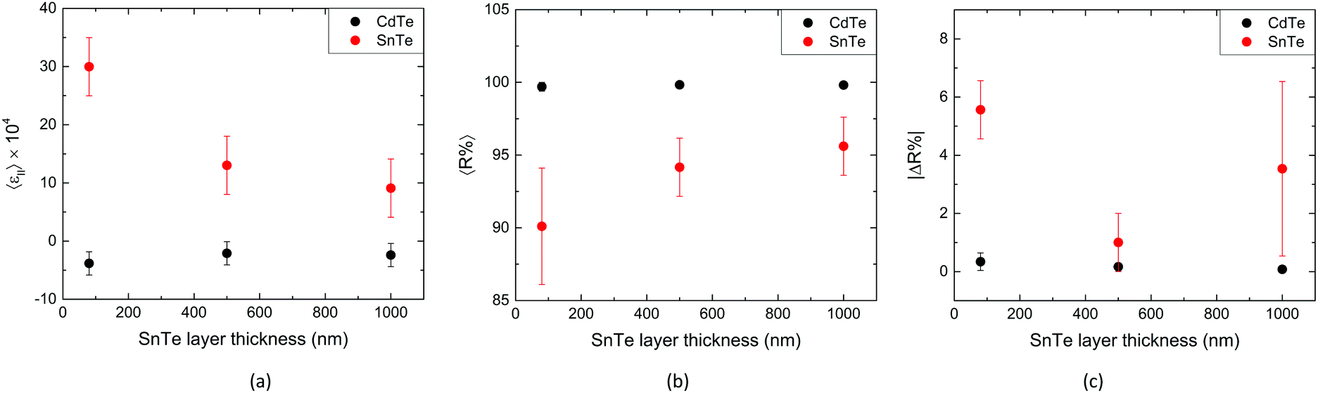 | ||
| Fig. 6 Influence of SnTe layer thickness on: (a) the mean horizontal strain in CdTe and SnTe; (b) the mean horizontal strain percentage relaxation in CdTe and SnTe; (c) the mean horizontal strain relaxation azimuthal anisotropy (φ = 0° vs. 90°) |ΔR%| in CdTe and SnTe. The results were twice averaged: for two perpendicular directions: [110] and [−110] and, afterward, for the groups of samples with respective SnTe layer thicknesses. | ||
On the basis of the values of C11 and C12 for CdTe and SnTe it was possible to predict that in the case of CdTe the absolute values of the vertical and horizontal strains should be comparable but in SnTe the horizontal strain modulus should be over 30 times greater than the vertical one. Indeed, for the buffer layer, determined absolute values of ε⊥ and ε‖ are comparable. They are also low: ε⊥ does not exceed 7.6 × 10⁻⁴ and ε‖ does not decline below −9.81 × 10⁻⁴. Moreover, the results confirm that the strain in CdTe does not depend significantly on the SnTe layer thickness, see Fig. 6a. The average value of the horizontal strain is −2.8 × 10⁻⁴. It follows that CdTe is almost fully relaxed. The relaxation reaches the average value 〈R%〉 = 99.8%, and only slight or negligible azimuthal anisotropy (φ = 0° vs. 90°) of horizontal strain and relaxation: Δ〈ε‖〉 = 2.5 × 10⁻⁴ and Δ〈R%〉 = 0.2% occurs in the buffer.
However, there is a noticeable horizontal strain in SnTe, dependent on the layer thickness and the largest in the samples with the thinnest layer (80 nm), see Fig. 6a. The extreme measured values of the strain are: −2.5 × 10⁻⁴ (minimum) and 46.4 × 10⁻⁴ (maximum), with 〈ε‖〉 = 17.4 × 10⁻⁴. The strain with a magnitude in the order of 1 × 10⁻³ is expected to be sufficient to cause opening of the energy gap in the spectrum of metallic topological surface states. The average azimuthal strain anisotropy Δ〈ε‖〉 is equal to 10.1 × 10⁻⁴, thus it is over four times larger than in CdTe. Relaxation of SnTe increases with the layer thickness, see Fig. 6b. The minimal value of it, averaged for the two orthogonal crystallographic directions [110] and [−110] is 86.2%. The average value of relaxation for the groups of samples with respective SnTe layer thicknesses amounts to 〈R%〉 = 93.3% and its average anisotropy Δ〈R%〉 = 3.4% (over seventeen times larger than in CdTe). The maximum measured anisotropy of the SnTe relaxation is ∼6.5%, see Fig. 6c.
To find a more complex model of the measured strain in CdTe and SnTe a thermal strain of those layers is taken into account, in a manner described in the ESI.† The calculated magnitude of the horizontal thermal strain in CdTe is in the order of 1 × 10⁻⁴ (with the assumption that α = 6 × 10⁻⁶ 1/K). It is negligible, because α coefficients in CdTe and GaAs are comparable, see Table 1. In SnTe, the horizontal thermal strain is in the order of 40.6 × 10⁻⁴. As easily noticed, the values of the measured horizontal strain in CdTe are negative, hence it must be caused not by the difference of its thermal expansion coefficient in relation to the GaAs substrate (which would give positive values), but by another factor; probably by the bilateral compression of CdTe by GaAs and SnTe (as both have unit cells smaller than CdTe), and that force not only offsets the negligible thermal strain in CdTe but furthermore results in its own, excessive strain.
The measured horizontal strain present in SnTe is positive and slightly smaller than the expected value of thermal strain ∼40 × 10−4. Its reduction may be caused by a relaxation process, which starts already during the growth of the layer. Hence, the horizontal strain in SnTe can be interpreted as a residual thermal strain. The values of micro-strain, calculated on the grounds of the Williamson–Hall plots (see the ESI†) are comparable with the values of vertical strain; they are in the order of 10−4 for both the CdTe and SnTe layers. The plots also provide information about the presence of micromosaics – the grains have size ca. 50–100 nm (in CdTe) and 30–60 nm (in SnTe).
Morphology of the samples
To check the initial surface morphology, AFM inspection of the reference CdTe buffer layer was carried out. The reference sample was only thermally treated at around 250 °C to desorb a protective amorphous tellurium layer. This uncovered CdTe buffer layer reveals a grainy surface without any additional visible structures at this scale (2 μm × 2 μm, see Fig. 7a). | ||
| Fig. 7 Atomic force microscopy images of the reference sample (only CdTe buffer layer), (001) oriented surface at different scales: (a) 2 × 2 μm; (b) 10 × 10 μm; (c) 50 × 50 μm. Cross-sections of the sample with 1000 nm SnTe grown at molecular flux ratio Te/SnTe = 0.0051 along one of {110} crystallographic planes, scales: (d) 10 × 10 μm; (e) 6 × 6 μm. The SnTe cross-section, visible in (e), has a ragged surface because it is cut not along the easy cleavage crystallographic direction (it is different in SnTe than in CdTe or GaAs: 〈100〉 vs. 〈110〉). | ||
The mean planar size of the randomly arranged grains is about 44.7 nm. AFM images on a larger scale (10 μm × 10 μm and 50 μm × 50 μm) show broad (width ca. 3 μm) ridges arranged along the crystallographic direction close to 〈110〉 (see Fig. 7b and c).
In the sample with a 1000 nm SnTe layer grown at molecular flux ratio Te/SnTe = 0.0051 the cross section along one of the {110} crystallographic planes (perpendicular to the surface) shows that numerous defects of CdTe are present (see Fig. 7d, upper part of the image). They create slightly bent lines and we suppose that on the intersection surface we are dealing with an image of the side surfaces of the column, slightly twisted in relation to each other.
A similar picture to that shown in Fig. 7d was shown in ref. 83 where the authors analysed the growth of CdTe by the sputtering technique at room temperature. There, too, the vertical lines at the cleavage were associated with the columnar growth of grains. Very similar images are typically obtained for the AFM cross section of the GaN layer columnar grown on a sapphire (00.1) substrate.84
As is known from the literature, numerous edge Lomer dislocations must be present in CdTe. It was previously determined via TEM that this kind of dislocation, having a 1/2[1−10] component in their Burgers vector, accommodates most of the misfit at the CdTe/GaAs interface, together with only a small amount of 60° dislocations (about 90% vs. 10%).85,86 Generally, Lomer dislocations are interpreted as two associated 60° dislocations from various {111} crystallographic planes86 and some of them undergo dissociation into 60° dislocations.85 As was stated, around the Lomer dislocations large crystal lattice distortion occurs.85 In the CdTe layer other dislocations were also detected, located at a distance of 20–25 nm from the interface, lying in the (1−11) plane and having 1/2[0 −1−1] and 1/2[10−1] components in their Burgers vector.85
Similarly to the reference sample with only a CdTe buffer layer, the sample with the thinnest SnTe layer (20 nm) has a surface with pronounced tiny seeds, but they are slightly bigger than the grains on the CdTe buffer surface – their widths reach around 100 nm (see Fig. 8a). Also, for samples with an 80 nm SnTe layer and the lowest molecular flux ratio Te/SnTe = 0, tiny seeds are observed (see Fig. 8d), however they start to arrange themselves.
 | ||
| Fig. 8 Atomic force microscopy images (scale 2 × 2 μm) of two series of samples with increasing SnTe layer thickness (described in the picture), grown at 310 °C at various Te/SnTe molecular beam flux ratios: (a–c) Te/SnTe = 0.0093; (d–f) Te/SnTe = 0. | ||
As the thickness of the SnTe layer or Te/SnTe molecular beam flux ratio increase, the seeds undergo a coalescence and form ripple-like elongated structures. It is clearly noticeable in Fig. 8b that these objects consist of small square-shaped grains. We found that the nanoripples are (statistically) ordered mainly along 〈100〉 and rarely on the 〈120〉 (inclined of ∼26° from 〈100〉 and ∼18° from 〈110〉) crystallographic direction (see Fig. 8b, c, e and f). Within the given sample with such developed morphology, the planar width of nanoripples is quite uniform, (190 ± 10) nm. The predominant direction of these nanostructures (〈100〉 or 〈120〉) does not correlate with the GaAs off-cut direction, because the azimuthal angles (φ) of the off-cut are the same for all the samples within the limit of error (±4°).
For the samples with thick SnTe layers (500 nm or 1000 nm) the nature of surface morphology evolution does not depend on the Te/SnTe molecular flux ratio. A set of samples grown with different ratios of molecular beam fluxes (0 or 0.0093) show similar transition from square-shaped grains into nanoripples (see Fig. 8). However, at a higher Te/SnTe molecular flux ratio slightly narrower nanoripples are formed for the same SnTe layer thickness (see, for example, Fig. 8bvs.Fig. 8e). This may indicate an influence of the additional Te molecular flux on the final quality of the sample's surface. The nanoripples’ width also seems to be dependent on the SnTe unit cell distortion – for the tetragonal type the nanostructures are narrower than for the monoclinic one (see Fig. 9, and also other AFM images, shown in the ESI†).
 | ||
| Fig. 9 Atomic force microscopy images (scale 1 × 1 μm) of samples with the same thickness of SnTe layer (500 nm) and different unit cell distortion type: (a) tetragonal; (b) monoclinic. The edges of each image and the axis are parallel to the 〈110〉 crystallographic directions. | ||
As is easy to notice, the nanostructures shown in Fig. 9a are made up of regular, square-like islands, grown in a symmetrical manner but the nanostructures visible in Fig. 9b have an elongated shape, disclosing different growth routes, with a significant tendency to coalesce the islands toward the 〈110〉 directions. On the nanoripples’ surface of some samples the atomic steps (∼0.3–0.6 nm high) are visible, see Fig. 10.
 | ||
| Fig. 10 Atomic force microscopy images of a sample with 80 nm SnTe, grown at molecular flux ratio Te/SnTe = 0: (a) scale 1 × 1 μm; (b) scale 0.4 × 0.4 μm; (c) section with shown atomic step heights (∼0.3–0.6 nm), depicting the area assigned by the blue line in (b). | ||
The quantitative data taken from AFM are shown in Fig. 11. They disclose that the mean roughness (image Rq parameter) of the samples with tetragonal distortion of SnTe noticeably increases with the layer thickness (see Fig. 11a). In the case of monoclinic deformation the range of Rq changes is much smaller; the parameter reaches a maximum for 500 nm thickness of SnTe and then declines, see Fig. 11a.
 | ||
| Fig. 11 Influence of SnTe layer thickness on: (a) mean sample surface roughness (Rq parameter); (b) nanostructure width (spectral period). (c) Surface nanostructure width (spectral period) as a function of γ angle in the SnTe unit cell. Investigated area enfolds 2 × 2 μm for all AFM measurements. The square-shaped point in the plot (c) refers to the data measured for the sample with SnTe unit cell distortion which may be interpreted as situated on the border of tetragonal and monoclinic type (it is the sample related to the on line point in Fig. 4c). | ||
Similarly, the mean width of nanoripples (spectral period parameter) exhibits a statistical tendency to increase with an increase of the layer thickness (see Fig. 11b) however the character of the changes is different for tetragonal and monoclinic distortion of the SnTe unit cell. For the first type the width of nanoripples increases at the SnTe thickness of 1000 nm, whereas for the second one a maximum of the spectral period parameter occurs at the SnTe thickness of 500 nm. The mean width of nanoripples is also dependent on the magnitude of the gamma angle aberrance in the SnTe unit cell from the value of 90°, see Fig. 11c. For a small aberrance (∼0.04°) from this angle, the spectral period is also quite small; see the square-shaped point in Fig. 11c. Next, the spectral period arises to reach the maximum at the Δγ close to 0.053° and to drop slowly above this value.
Azimuthal defect distribution and dislocation density in the CdTe buffer and SnTe layer
Knowing that the half-width of the rocking curve is partly influenced by linear defects we use the term azimuthal defect distribution to show the dependence of RC FWHM on azimuthal angle for all symmetric reflections for both CdTe and SnTe layers in two exemplary samples with 1000 nm SnTe, grown at Te/SnTe molecular flux ratios of 0.0089 and 0.0051 (see Fig. 12 with plots based on a 006 reflection; more plots are shown in the ESI†).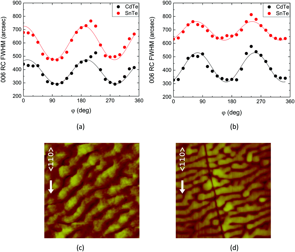 | ||
| Fig. 12 Dependence of 006 RC FWHM on azimuthal angle in CdTe and SnTe layers and atomic force microscopy images (scale: 2 × 2 μm) for two exemplary samples with the same 1000 nm thick SnTe layers: (a and c) sample grown at molecular flux ratio Te/SnTe = 0.0089, nanoripples close to 〈100〉; (b and d) samples grown at ratio Te/SnTe = 0.0051, nanoripples close to 〈120〉. | ||
As can be seen, there occur pronounced and regular FWHM fluctuations, which denote azimuthal anisotropy of defect distribution in the investigated samples. Moreover, the shape of FWHM fluctuations for CdTe is exactly repeated by the curve corresponding to SnTe, they differ only in the amplitude. That is a fingerprint of a reproduction of defect distribution in buffer by the SnTe layer.
Of course, the fluctuations of RC FWHM are partially influenced also by the azimuthal dependence of the off-cut angle and by the measured reflection (as shown by the formula quoted in the ESI from ref. 87); however, in the case of our samples this impact is significantly smaller than the changes caused by the defect distribution anisotropy. For example, for 006 reflection the calculated FWHM fluctuation amplitudes due to the off-cut are in the sample grown at molecular flux ratio Te/SnTe = 0.0051:25′′ for CdTe and 42′′ for SnTe and in the sample grown at ratio Te/SnTe = 0.0089:22′′ for CdTe and 34′′ for SnTe. Thus, they can be ignored in the interpretation of the results (full analysis illustrated with plots is presented in the ESI†).
Applying Ayers plots (FWHM2 as a function of tan2θ88) we estimated the maximum and minimum dislocation density (D) in CdTe and SnTe layers (details in the ESI†). As easily noticed, the value of D calculated from this plot depends on the azimuthal angle (it results from the dependence of FWHM on the azimuthal angle). The D maxima and minima were determined by fitting the experimental FWHM curves with a sine function, as shown by the example for 006 reflections in Fig. 12. The estimated maximal and minimal D values in the samples grown at Te/SnTe = 0.0051 and Te/SnTe = 0.0089 are tabularized in Table 2. It is easy to notice that for both CdTe and SnTe in the minimum and the maximum of the curve from Fig. 12 there is about two-fold difference in the dislocation density.
| Sample | Te/SnTe = 0.0051 | Te/SnTe = 0.0089 | ||
|---|---|---|---|---|
| Layer | CdTe | SnTe | CdTe | SnTe |
| D minimal × 10−8 [cm−2]/φ | 1.5 ± 1/∼158° | 5 ± 5/∼161° | 1.6 ± 0.4/∼102° | 7 ± 3.5/∼96° |
| D maximal × 10−8 [cm−2]/φ | 6 ± 0.7/∼75° | 12 ± 4/∼70° | 3.5 ± 2/∼11° | 16 ± 2/∼0° |
Presumable mechanism of SnTe surface nanoripples formation during the layer growth
We infer that the mechanism of SnTe surface nanoripples formation can be dislocation-driven and is perhaps also related to the CdTe buffer layer defect structure and its surface morphology.It is known from the literature that lattice mismatched zinc blende semiconductor layers, such as CdTe/GaAs, first accommodate the lattice misfit by a tetragonal homogenous strain in the epilayer. The grown layer is pseudomorphic until the thickness of the layer exceeds the critical thickness, which is 1.2 nm (∼4 monolayers) for ZnTe/GaAs89 and 1.6 nm (∼5 monolayers) for CdTe/ZnTe.90 The second factor boosting the lattice distortion is the difference in the thermal expansion coefficients between the layer and the substrate, e.g. CdTe/GaAs.47 After achieving a critical thickness the strain starts to relax by generation of 60° misfit dislocations at the interface.48
However, most of the misfit at the CdTe/GaAs interface is relaxed by the edge Lomer dislocations,85,86 consisting of two associated 60° dislocations.85,86 With increasing layer thickness the threading dislocation lines develop with a slip.91
It was reported that if the mismatch between the substrate and the epilayer is larger than 3%, the growth of the layer is consistent with the Stranski–Krastanov mode, where relaxation is manifested as island formation rather than by misfit dislocations.90
Another mechanism of the strongly mismatched layer relaxation process, proposed for the ZnTe/GaAs(001) heterostructure,89 involves a growth mode transition from 2D to 3D. According to that model a nucleation of many islands occurs, especially in the case of compounds with a short diffusion length (typical for II–VI compounds) grown on a substrate with a large density of kink-sites. Next, when the layer reaches the critical thickness it starts to relax the accumulated strain. The relaxation suppresses the Stranski–Krastanov growth mode, increases the growth rate and brings on coalescence of the islands. The above mentioned processes – islands creation, strain relaxation and islands coalescence are competing during the development of the surface morphology. It was determined that the 3D growth mode causes expansion of {n11} planes and surface ridges arise along the [1−10] crystallographic direction in thick ZnTe layers.89 These results are in good agreement with our observation of the broad ripples along the 〈110〉 crystallographic direction on the surface of the CdTe buffer layer (shown in Fig. 7b and c). However, the ripples in our case are much broader than those described in ZnTe (∼3 μm vs. ∼0.4 μm).
In thick CdTe (or ZnTe) layers on GaAs a periodic distribution of misfit dislocations and anisotropic relaxation of the layer occur. There the density of [−110]-oriented dislocations is higher than that of the [110]-oriented ones. This is caused by the lower energy barrier formation of this kind of dislocation, as well as by a higher mobility in the [−110] crystallographic direction.51 This phenomenon is determined by a different structure of the dislocation core (based on another chemical element) and leads to the anisotropic broadening of the recorded rocking curves of symmetrical 004 reflection. In the CdTe strain relaxation processes the GaAs substrate off-cut is also involved, similarly to that reported for InxGa1−xAs layers on GaAs.92 It was also observed that the [−110] crystallographic direction is energetically favoured in GaAs as the direction along which Mn dimers in (Ga, Mn)As are created.93
During the first stage of SnTe growth, SnTe nucleation occurs, spread over the whole sample surface. This process is promoted by a buffer layer surface roughness which is a source of kink-sites and thus inhibits the diffusion, similarly to the ZnTe in the GaAs case.89 According to the results of other investigations, in a thin (∼1 nm) rock-salt structured layer deposited on an immiscible zinc blende host material formation of quantum dots via a self-organization process is possible.94 Thus, an initial generation of SnTe islands on the CdTe surface seems to be highly probable. It was reported that the first ∼4 monolayers of SnTe can grow in the zinc blende structure forced by the crystal structure of the CdTe buffer layer. Subsequently, whereas the SnTe layer becomes thicker, the relaxation takes places and its crystal structure transforms into a stable rock-salt one, as was observed for SnTe/CdTe(110)95 grown along the 〈110〉 direction.
The misfit dislocations created in the CdTe buffer seem to affect defects in the SnTe layer. This is visible as inclined lines in the upper parts of the image in Fig. 7e. For thick-capped layers the threading dislocations can form so-called dislocation dipoles consisting of pairs of dislocations at the CdTe/GaAs and SnTe/CdTe interfaces.96 A new dislocations relaxing lattice misfit at the SnTe/CdTe interface (2.5%, the forces are tensile for the SnTe lattice) are expected as well. However the latter misfits are significantly smaller than the former ones (14.7%, the forces are compressive for the CdTe lattice). As shown by us, the defect structure of the CdTe buffer is reproduced by SnTe. Moreover, the azimuthal angles of the FWHM maxima can be interpreted as associated with the nanoripples with predominant [100] or [120] directions, because it is visible that the angles in the sample with 1000 nm SnTe grown at molecular flux ratio Te/SnTe = 0.0051 are shifted in comparison to the sample grown at ratio Te/SnTe = 0.0089, which is correlated with the difference of the nanoripples’ direction (compare the sine plots and AFM images in Fig. 12).
The change in the surface morphology associated with the SnTe layer thickness, illustrated in Fig. 8 for two series of samples, can be interpreted as dislocation-driven. The relaxation processes locally improve the growth (i.e. in the meaning of the crystal structure) in the area above the dislocations and as a result cause an enhancement of the surface corrugation.97 The differences in the nanoripple widths depend on the Te/SnTe molecular flux ratio and can be associated with the tendency to a weaker development of the (001) surface than the (111) one under conditions of Te-rich crystal growth.98 It is possible that a lateral growth via (111) planes occurs.
We could assume also a possibility of migration and ordering of the small grains along the 〈110〉 crystallographic directions while the dislocation slides. A similar mechanism of evolution of the surface morphology was observed in SnTe single microcrystals grown by chemical vapor deposition (CVD).99 The authors observed migration of small surface pits and merging to form more complicated nanostructures. However, during the CVD growth the temperature was much higher than the growth temperature of our samples (500 °C vs. ∼300 °C) thus the diffusion and migration processes reported in ref. 98 were probably more efficient than in our crystals.
The final shape of the nanostructures can be influenced by the interactions between complementary 60° dislocations coming from the CdTe buffer layer. Four possible types of such interactions are described for films grown on (001) oriented substrates.100
An alternative mechanism of nanoripple creation can be based on a so-called meandering process, driven by diffusion and a Schwöbel barrier. Such a phenomenon was described for the GaN(000−1) surface.101 The diffusion-driven mechanism of self-organization of other nanostructures was observed and simulated in PbTe/CdTe multilayers.102,103 However, in such a case the nanoripples should not be formed, and in particular they would not consist of square-shaped grains as is observed in Fig. 8b. Moreover, the azimuthal anisotropy of RC FWHM is not predicted in this mechanism. Thus, the mechanisms based on diffusion only seem to be excluded. Whereas it is expected that the diffusion anisotropy can affect the shape of SnTe seeds at the early stage of layer growth on a CdTe surface. We suppose that the dislocation driven mechanisms play an important role when the SnTe layer is thick enough (over ∼4 monolayers). We attribute the CdTe/GaAs lattice misorientation to the strain relaxation anisotropy during CdTe buffer layer growth. This anisotropy is determined by the difference in dislocation mobility toward the [110] and [−110] crystallographic directions.
Another alternative mechanism for nanoripple growth would be based on step-bunching, but it can also be excluded, for two reasons. First, SnTe nanoripples are dramatically broader than the estimated GaAs terrace width (180 nm–200 nm vs. only 40 Å). Second, SnTe does not grow directly on GaAs terraces but on the CdTe surface, shaped into its own ripples, arranged toward the 〈110〉, not toward the 〈100〉 direction.
Conclusions
The results of our studies show that in the MBE-grown SnTe/CdTe(001) heterostructures the rock-salt SnTe layer and the zinc blende CdTe buffer undergo a tetragonal crystal distortion, almost fully relaxed by the formation of misfit dislocations at the interfaces. In SnTe the azimuthal strain anisotropy occurs with an average value equal to 6.1 × 10⁻⁴, whereas in CdTe it is about twelve times smaller. There is a noticeable CdTe/GaAs crystal lattice misorientation up to 0.8° with a change of azimuthal angle up to 23° and an anisotropic defect distribution.The relaxation of the materials constituting the investigated heterostructures is almost complete – only some residual thermal strain in SnTe and small negative strain in CdTe occur, which is probably caused by the bilateral compression of CdTe between GaAs and SnTe. The relaxation in SnTe is slightly anisotropic, up to ∼6.5%, which may be caused by a lower mobility of dislocations toward the [110] crystallographic direction in comparison to the [−110] one. In some samples monoclinic deformation of the SnTe unit cell is observed with the γ angle deviation from 90° in the range of 0.041–0.119°. This seemingly small deformation actually importantly changes the crystal symmetry of the TCI SnTe layer, thus lowering it from the four-fold to the two-fold one.
The samples’ surface morphology is diversified depending on the thickness of the SnTe layer. The thinnest (20 nm or 80 nm) layers are characterized by the surface structure composed of randomly distributed grains. With increasing SnTe layer thickness the nanoripples start to appear on the (001) surface, along distinct crystallographic directions: 〈100〉 or 〈120〉. The mechanism of nanoripple formation is dislocation-driven. At the first stage, it involves the generation of small grains, which next coalesce due to a local improvement in the crystal growth in the area above the dislocations or migrate with dislocations to join together and mold into the extended forms of nanoripple.
For a higher Te/SnTe molecular flux ratio, slightly narrower nanoripples are formed (for the same thickness of SnTe layer). Narrower nanoripples are observed for the tetragonal type of distortion, for thinner layers, and for small γ aberrance (∼0.04°). Above the aberrance of about 0.053° the spectral period of nanostructures slowly drops.
The observed anisotropy of crystal defect distribution in SnTe layers grown on a CdTe (001)/GaAs substrate can be a source of lowering the crystal symmetry, therefore influencing the protection mechanism warranting the existence of TCI states. Breaking one of the {110} mirror plane symmetries protecting the TCI states is known to open the energy gap in the metallic Dirac-like spectrum of surface states resulting in a transition to topologically trivial state. The measured monoclinic distortion in SnTe(001) layers (lattice strain ∼10−3) is large enough to cause the opening of such an energy gap. Detailed analysis of the symmetry and morphology of the SnTe layer surface is also of critical importance for implementation of one-dimensional topological states recently found experimentally along atomic steps of odd monolayer height on the (001) surface of the closely related TCI IV-VI materials system, Pb1−xSnxSe.104,105 Thus, the monoclinic deformation in the samples investigated by us may be useful from the point of view of spintronics because it can serve as an additional degree of freedom or a control parameter in devices based on various SnTe, Pb1−xSnxTe, and Pb1−xSnxSe layered heterostructures.
Author contributions
Adrian Sulich: conceptualization (the idea of an article), investigation (part of the HR XRD studies), formal analysis (calculations, interpretation of the SnTe surface nanoripples formation mechanism), visualization (most of the figures, Tables 1 and 2) and writing – original draft; Elżbieta Łusakowska: investigation (AFM studies), visualization (AFM images); Wojciech Wołkanowicz, Piotr Dziawa and Badri Taliashvili: resources (growth of the investigated samples); Tomasz Story and Tomasz Wojtowicz: supervision (coordination of the sample growth); Jaroslaw Z. Domagala: investigation (part of the HR XRD studies), methodology (the method of the crystal unit cell monoclinic deformation measurement), visualization (Fig. 1) and supervision (coordination of experimental works). The authors that contributed to validation of the obtained results: Adrian Sulich, Jaroslaw Z. Domagala, Elżbieta Łusakowska, Piotr Dziawa, Tomasz Story, Wojciech Wołkanowicz, and Janusz Sadowski. The authors involved in writing – review & editing: Adrian Sulich, Piotr Dziawa, Tomasz Story, Jaroslaw Z. Domagala, and Janusz Sadowski.Conflicts of interest
There are no conflicts to declare.Acknowledgements
This research was partially supported by the Foundation for Polish Science through the International Research Agendas Programme co-financed by the EU within SG OP (Tomasz Story, Tomasz Wojtowicz) and by the National Science Centre (Poland) research project UMO 2017/27/B/ST3/02470 (Elżbieta Łusakowska, Wojciech Wołkanowicz), and UMO-2019/35/B/ST3/03381 (Piotr Dziawa and Janusz Sadowski).References
- G. Tan, F. Shi, S. Hao, H. Chi, T. P. Bailey, L. D. Zhao, C. Uher, Ch Wolverton, V. P. Dravid and M. G. Kanatzidis, J. Am. Chem. Soc., 2015, 137(35), 11507 CrossRef CAS PubMed.
- L. Fu, Phys. Rev. Lett., 2011, 106(10), 106802 CrossRef PubMed.
- T. H. Hsieh, H. Lin, J. Liu, W. Duan, A. Bansil and L. Fu, Nat. Commun., 2012, 3, 982 CrossRef PubMed.
- J. E. Moore, Nature, 2010, 464(7286), 194 CrossRef CAS PubMed.
- P. Dziawa, B. J. Kowalski, K. Dybko, R. Buczko, A. Szczerbakow, M. Szot, E. Łusakowska, T. Balasubramanian, B. M. Wojek, M. H. Berntsen, O. Tjernberg and T. Story, Nat. Mater., 2012, 11(12), 1023 CrossRef CAS PubMed.
- K. Sun, Nat. Mater., 2015, 14(3), 262 CrossRef CAS PubMed.
- Y. Ando and L. Fu, Annu. Rev. Condens. Matter Phys., 2015, 6(1), 361 CrossRef CAS.
- K. Dybko, M. Szot, A. Szczerbakow, M. U. Gutowska, T. Zajarniuk, J. Z. Domagala, A. Szewczyk, T. Story and W. Zawadzki, Phys. Rev. B, 2017, 96, 205129 CrossRef.
- B. M. Wojek, M. H. Berntsen, V. Jonsson, A. Szczerbakow, P. Dziawa, B. J. Kowalski, T. Story and O. Tjernberg, Nat. Commun., 2015, 6, 8463 CrossRef CAS PubMed.
- Y. Okada, M. Serbyn, H. Lin, D. Walkup, W. Zhou, C. Dhital, M. Neupane, S. Xu, Y. J. Wang, R. Sankar, F. Chou, A. Bansil, M. Z. Hasan, S. D. Wilson, L. Fu and V. Madhavan, Science, 2013, 341, 1496 CrossRef CAS PubMed.
- Y. Tanaka, Z. Ren, T. Sato, K. Nakayama, S. Souma, T. Takahashi, K. Segawa and Y. Ando, Nat. Phys., 2012, 8, 800 Search PubMed.
- S.-Y. Xu, C. Liu, N. Alidoust, M. Neupane, D. Qian, I. Belopolski, J. D. Denlinger, Y. J. Wang, H. Lin, L. A. Wray, G. Landolt, B. Slomski, J. H. Dil, A. Marcinkova, E. Morosan, Q. Gibson, R. Sankar, F. C. Chou, R. J. Cava, A. Bansil and M. Z. Hasan, Nat. Commun., 2012, 3, 1192 Search PubMed.
- J. Shen, Y. Jung, A. S. Disa, F. J. Walker, C. H. Ahn and J. J. Cha, Nano Lett., 2014, 14(7), 4183 CrossRef CAS PubMed.
- S. Safaei, P. Kacman and R. Buczko, Phys. Rev. B, 2013, 88, 045305 CrossRef.
- M. J. Gilbert, Commun. Phys., 2021, 4, 70 CrossRef CAS.
- C. Yue, S. Jiang, H. Zhu, L. Chen, Q. Sun and D. W. Zhang, Electronics, 2018, 7, 225 CrossRef CAS.
- F. Schindler, A. M. Cook, M. G. Vergniory, Z. Wang, S. S. P. Parkin, B. A. Bernevig and T. Neupert, Sci. Adv., 2018, 4, eaat0346 CrossRef PubMed.
- S. H. Kooi, G. van Miert and C. Ortix, Phys. Rev. B, 2020, 102, 041122(R) CrossRef.
- M. Serbyn and L. Fu, Phys. Rev. B, 2014, 90, 035402 CrossRef CAS.
- I. Zeljkovic, Y. Okada, M. Serbyn, R. Sankar, D. Walkup, W. Zhou, J. Liu, G. Chang, Y. J. Wang, M. Z. Hasan, F. Chou, H. Lin, A. Bansil, L. Fu and V. Madhavan, Nat. Mater., 2015, 14, 318 CrossRef CAS PubMed.
- Q. Zhang, B. Liao, Y. Lan, K. Lukas, W. Liu, K. Esfarjani, C. Opeil, D. Broido, G. Chen and Z. Ren, Proc. Natl. Acad. Sci. U. S. A., 2013, 110(33), 13261 CrossRef CAS PubMed.
- K. Chang, T. P. Kaloni, H. Lin, A. Bedoya-Pinto, A. K. Pandeya, I. Kostanovskiy, K. Zhao, Y. Zhong, X. Hu, Q.-K. Xue, X. Chen, S.-H. Ji, S. Barraza-Lopez and S. S. P. Parkin, Adv. Mater., 2019, 31, 1804428 CrossRef PubMed.
- G. Balakrishnan, L. Bawden, S. Cavendish and M. R. Lees, Phys. Rev. B, 2013, 87, 140507 CrossRef.
- G. Xie, Z. Li, T. Luo, H. Bai, J. Sun, Y. Xiao, L.-D. Zhao, J. Wu, G. Tan and X. Tang, Nano Energy, 2020, 69, 104395 CrossRef CAS.
- W. W. Yu, L. Qu, W. Guo and X. Peng, Chem. Mater., 2003, 15(14), 2854 CrossRef CAS.
- X. Wu, Sol. Energy, 2004, 77, 803 CrossRef CAS.
- D. Yue, X. Qian, Z. Zhang, M. Kan, M. Ren and Y. Zhao, ACS Sustainable Chem. Eng., 2016, 4, 6653 CrossRef CAS.
- J. Peng, Q. Huang, Y. Liu, P. Liu and C. Zhang, Sens. Actuators, B, 2019, 294, 157 CrossRef CAS.
- H. Ohno, A. Shen, F. Matsukura, A. Oiwa, A. Endo, S. Katsumoto and Y. Iye, Appl. Phys. Lett., 1996, 69, 363 CrossRef CAS.
- S. Adachi, J. Appl. Phys., 1985, 58(3), R1 CrossRef CAS.
- D. Jung, P. G. Callahan, B. Shin, K. Mukherjee, A. C. Gossard and J. E. Bowers, J. Appl. Phys., 2017, 122, 225703 CrossRef.
- L. Balaghi, G. Bussone, R. Grifone, R. Hübner, J. Grenzer, M. Ghorbani-Asl, A. V. Krasheninnikov, H. Schneider, M. Helm and E. Dimakis, Nat. Commun., 2019, 10(1), 2793 CrossRef PubMed.
- P. L. Moody, H. C. Gatos and M. C. Lavine, J. Appl. Phys., 1960, 31(9), 1696 CrossRef CAS.
- H. A. Mar, K. T. Chee and N. Salansky, Appl. Phys. Lett., 1984, 44(2), 237 CrossRef.
- J. N. Zemel, J. D. Jensen and R. B. Schoolar, Phys. Rev., 1965, 140(1A), A330 CrossRef.
- A. E. Muslimov, A. V. Butashin, V. I. Mikhailov, I. M. Shapiev, A. M. Ismailov, E. G. Novoselova, I. S. Smirnov and V. M. Kanevsky, Crystallogr. Rep., 2015, 60(4), 561 CrossRef CAS.
- W. J. Yin, J. H. Yang, K. Zaunbrecher, T. Gessert, T. Barnes, Y. Yan and S. H. Wei, Appl. Phys. Lett., 2015, 107(14), 141607 CrossRef.
- K. Tang, X. Zhu, W. Bai, L. Zhu, J. Bai, W. Dong, J. Yang, Y. Zhang, X. Tang and J. Chu, J. Alloys Compd., 2016, 685, 370 CrossRef CAS.
- M. F. Vargas-Charry and C. Vargas-Hernández, Mater. Sci. Semicond. Process., 2015, 31, 561 CrossRef CAS.
- J. Wang, N. Wang, H. Huang and W. Duan, Chin. Phys. B, 2016, 25(11), 117313 CrossRef.
- M. Saghir, M. R. Lees, S. J. York, S. A. Hindmarsh, A. M. Sanchez, M. Walker, C. F. McConville and G. Balakrishnan, J. Indian Inst. Sci., 2016, 96(2), 121 Search PubMed.
- Z. Li, S. Shao, N. Li, K. McCall, J. Wang and S. X. Zhang, Nano Lett., 2013, 13(11), 5443 CrossRef CAS PubMed.
- M. G. Williams, R. D. Tomlinson and M. J. Hampshire, Solid State Commun., 1969, 7(24), 1831 CrossRef CAS.
- T. F. Smith, J. A. Birch and J. G. Collins, J. Phys. C-Solid State Phys., 1976, 9, 4375 CrossRef CAS.
- P. Bauer Pereira, I. Sergueev, S. Gorsse, J. Dadda, E. Mueller and R. P. Hermann, Phys. Status Solidi B, 2013, 250(7), 1300 CrossRef CAS.
- N. Berchenko, R. Vitchev, M. Trzyna, R. Wojnarowska-Nowak, A. Szczerbakow, A. Badyla, J. Cebulski and T. Story, Appl. Surf. Sci., 2018, 452, 134 CrossRef CAS.
- H. Tatsuoka, H. Kuwabara, H. Fujiyasu and Y. Nakanishi, J. Appl. Phys., 1989, 65(5), 2073 CrossRef CAS.
- K. Wichrowska, J. Z. Domagala, T. Wosinski, S. Chusnutdinow and G. Karczewski, Acta Phys. Pol., A, 2014, 126(5), 1083 CrossRef.
- H. Tatsuoka, H. Kuwabara, Y. Nakanishi and H. Fujiyasu, J. Appl. Phys., 1990, 67(11), 6860 CrossRef CAS.
- J. F. Wang, K. Kikuchi, B. H. Koo, Y. Ishikawa, W. Uchida and M. Isshiki, J. Cryst. Growth., 1998, 187(3–4), 373 CrossRef CAS.
- J. Domagała, J. Bąk-Misiuk, J. Adamczewska, Z. R. Zytkiewicz, E. Dynowska, J. Trela, D. Dobosz, E. Janik and M. Leszczyński, Phys. Status Solidi A, 1999, 171(1), 289 CrossRef.
- M. E. Straumanis and C. D. Kim, Acta Crystallogr., 1965, 19(2), 256 CrossRef CAS.
- J. S. Blakemore, J. Appl. Phys., 1982, 53, R123 CrossRef CAS.
- M. K. Rabadanov, I. A. Verin, Y. M. Ivanov and V. I. Simonov, Kristallografiya, 2001, 46(4), 703 CrossRef CAS.
- S. Schreyeck, K. Brunner, L. W. Molenkamp, G. Karczewski, M. Schmitt, P. Sessi, M. Vogt, S. Wilfert, A. B. Odobesko and M. Bode, Phys. Rev. Mater., 2019, 3, 024203 CrossRef CAS.
- M. K. Rabadanov, Kristallografiya, 1995, 40(3), 505 CAS.
- B. H. Lee, J. Appl. Phys., 1970, 41, 2988 CrossRef CAS.
- M. Szot, K. Dybko, P. Dziawa, L. Kowalczyk, E. Smajek, V. Domukhovski, B. Taliashvili, P. Dłużewski, A. Reszka, B. J. Kowalski, M. Wiater, T. Wojtowicz and T. Story, Cryst. Growth Des., 2011, 11(11), 4794 CrossRef CAS.
- H. Nishino, S. Murakami and Y. Nishijima, Jpn. J. Appl. Phys., 1999, 38(10R), 5775 CrossRef CAS.
- E. J. Heller, Z. Y. Zhang and M. G. Lagally, Phys. Rev. Lett., 1993, 71(5), 743 CrossRef CAS PubMed.
- Y. Nabetani, A. Wakahara and A. Sasaki, J. Appl. Phys., 1995, 78(11), 6461 CrossRef CAS.
- M. D. Pashley, K. W. Haberern and J. M. Gaines, Appl. Phys. Lett., 1991, 58(4), 406 CrossRef CAS.
- H. Shtrikman, M. Oron, A. Raizman and G. Cinader, J. Electron. Mater., 1988, 17(2), 105 CrossRef CAS.
- H. A. Mar, R. Salansky and K. T. Chee, Appl. Phys. Lett., 1984, 44, 898 CrossRef CAS.
- H. Nishino, I. Sugiyama and Y. Nishijima, J. Appl. Phys., 1996, 80, 3238 CrossRef CAS.
- Z. Ren, Y. Lan and Q. Zhang, Advanced Thermoelectrics: Materials, Contacts, Devices, and Systems, CRC Press, 2017 Search PubMed.
- E. I. Rogacheva, G. V. Gorne, N. K. Jigareva and A. B. Ivanova, Izv. Akad. Nauk SSSR, Neorg. Mater., 1991, 27(2), 267 CAS.
- P. Y. Su, C. Lee, G. C. Wang, T. M. Lu and I. B. Bhat, J. Electron. Mater., 2014, 43(8), 2895 CrossRef CAS.
- U. A. Mengui, E. Abramof, P. H. O. Rappl and A. Y. Ueta, Braz. J. Phys., 2006, 36(2A), 324 CrossRef CAS.
- Y. G. Sidorov, M. V. Yakushev, V. S. Varavin, A. V. Kolesnikov, E. M. Trukhanov, I. V. Sabinina and I. D. Loshkarev, Phys. Solid State, 2015, 57(11), 2151 CrossRef CAS.
- Y. Sidorov, I. Loshkarev, I. Sabinina, E. Trukhanov, V. Varavin, M. Yakushev and A. Kolesnikov, Phys. Status Solidi C, 2016, 13(7–9), 425 CrossRef CAS.
- F. Riesz, J. Appl. Phys., 1996, 79, 4111 CrossRef CAS.
- D. J. Eaglesham, D. M. Maher, H. L. Fraser, C. J. Humphreys and J. C. Bean, Appl. Phys. Lett., 1989, 54, 222 CrossRef CAS.
- O. Yastrubchak, J. Bak-Misiuk, E. Łusakowska, J. Kaniewski, J. Z. Domagala, T. Wosiński, A. Shalimov, K. Regiński and A. Kudla, Phys. B, 2003, 340–342, 1082 CrossRef CAS.
- M. Krysko, J. Z. Domagala, R. Czernecki and M. Leszczynski, J. Appl. Phys., 2013, 114, 113512 CrossRef.
- O. Yastrubchak, T. Wosiński, J. Z. Domagała, E. Łusakowska, T. Figielski, B. Pecz and A. L. Tóth, J. Phys.: Condens. Matter, 2004, 16, S1 CrossRef CAS.
- O. Yastrubchak, J. Z. Domagała, T. Wosiński, A. Kudła and K. Regiński, Phys. Status Solidi C, 2005, 2(6), 1943 CrossRef CAS.
- S. Miotkowska, E. Dynowska, I. Miotkowski, A. Szczerbakow, B. Witkowska, J. Kachniarz and W. Paszkowicz, J. Cryst. Growth., 1999, 200, 483 CrossRef CAS.
- Semiconductors, ed. R. Poerschke, Springer, Berlin, 1992 Search PubMed.
- M. Martínez-Ripoll, http://www.xtal.iqfr.csic.es/Cristalografia/, Accessed 3 March 2021, Dept. de Cristalografia y Biol. Estruc. c/Serrano 119 E-28006 Madrid (Espania).
- D. G. Thomas, J. Appl. Phys., 1961, 32(10), 2298 CrossRef CAS.
- A. J. Miller, G. A. Saunders and Y. K. Yogurtcu, J. Phys. C-Solid State Phys., 1981, 14(11), 1569 CrossRef CAS.
- E. Camacho-Espinosa, E. Rosendo, T. Díaz, A. I. Oliva, V. Rejon and J. L. Peña, Superficies Vacio, 2014, 27(1), 15 Search PubMed.
- D. A. Stocker, E. F. Schubert, W. Grieshaber, K. S. Boutros and J. M. Redwing, Appl. Phys. Lett., 1998, 73(14), 1925 CrossRef CAS.
- S. Kret, D. Paweł, D. Piotr and J.-Y. Laval, Philos. Mag., 2003, 83(2), 231 CrossRef CAS.
- S. Kret, P. Dłużewski, P. Dłużewski and E. Sobczak, J. Phys.: Condens. Matter, 2000, 12, 10313 CrossRef CAS.
- D. K. Bowen and B. K. Tanner, High Resolution X-Ray Diffractometry and Topography, Taylor & Francis, London, Bristol, PA, 1998 Search PubMed.
- J. E. Ayers, J. Cryst. Growth., 1994, 135, 71 CrossRef CAS.
- M. Longo, N. Lovergine and A. M. Mancini, J. Vac. Sci. Technol., B: Nanotechnol. Microelectron.: Mater., Process., Meas., Phenom., 1998, 16, 2650 CrossRef CAS.
- K. Pinardi, S. C. Jain, H. E. Maes, R. Van Overstraeten and M. Willander, J. Appl. Phys., 1998, 83(9), 4724 CrossRef CAS.
- J. W. Matthews, S. Mader and T. B. Light, J. Appl. Phys., 1970, 41(9), 3800 CrossRef CAS.
- R. S. Goldman, K. L. Kavanagh, H. H. Wieder, S. N. Ehrlich and R. M. Feenstra, J. Appl. Phys., 1998, 83(10), 5137 CrossRef CAS.
- M. Birowska, C. Śliwa, J. A. Majewski and T. Dietl, Phys. Rev. Lett., 2012, 108(23), 237203 CrossRef CAS PubMed.
- H. Groiss, I. Daruka, K. Koike, M. Yano, G. Hesser, G. Springholz, N. Zakharov, P. Werner and F. Schäffler, APL Mater., 2014, 2, 012105 CrossRef.
- H. Höchst, D. W. Niles, M. A. Engelhardt and I. Hernández-Calderón, J. Vac. Sci. Technol., A, 1989, 7(3), 775 CrossRef.
- S. C. Jain, A. H. Harker and R. A. Cowley, Philos. Mag. A, 1997, 75(6), 1461 CAS.
- M. Albrecht, S. Christiansen, J. Michler, W. Dorsch, H. P. Strunk, P. O. Hansson and E. Bauser, Appl. Phys. Lett., 1995, 67, 1232 CrossRef CAS.
- V. L. Deringer and R. Dronskowski, ChemPhysChem, 2013, 14, 3108 CrossRef CAS PubMed.
- P. Liu, Y. Xie, E. Miller, Y. Ebine, P. Kumaravadivel, S. Sohn and J. J. Cha, J. Phys. Chem. Solids, 2019, 128, 351 CrossRef.
- Y. B. Bolkhovityanov, A. S. Deryabin, A. K. Gutakovskii and L. V. Sokolov, J. Appl. Phys., 2011, 109, 123519 CrossRef.
- F. Krzyżewski, M. A. Załuska-Kotur, H. Turski, A. Feduniewicz-Żmuda and C. Skierbiszewski, Numerical Study of Meandered Step Patterns at GaN(000-1) Surface, 2018, contributed lecture, 47th International School & Conference on the Physics of Semiconductors “Jaszowiec 2018”, Szczyrk.
- M. Mińkowski, M. A. Załuska-Kotur, S. Kret, S. Chusnutdinow, S. Schreyeck, K. Brunner and L. W. Molenkamp, J. Alloys Compd., 2018, 747, 809 CrossRef.
- M. Mińkowski, M. A. Załuska-Kotur, Ł. A. Turski and G. Karczewski, J. Appl. Phys., 2016, 120, 124305 CrossRef.
- P. Sessi, D. Di Sante, A. Szczerbakow, F. Glott, S. Wilfert, H. Schmidt, T. Bathon, P. Dziawa, M. Greiter, T. Neupert, G. Sangiovanni, T. Story, R. Thomale and M. Bode, Science, 2016, 354(6317), 1269 CrossRef CAS PubMed.
- J. Jung, A. Odobesko, R. Boshuis, A. Szczerbakow, T. Story and M. Bode, Phys. Rev. Lett., 2021, 126, 234402 CrossRef PubMed.
Footnote |
| † Electronic supplementary information (ESI) available. See DOI: 10.1039/d1tc05733b |
| This journal is © The Royal Society of Chemistry 2022 |