
 Open Access Article
 This Open Access Article is licensed under a
 Creative Commons Attribution 3.0 Unported Licence
Correlating the chemical structure and charge transport ability of dibenzofulvene-based hole transporting materials for stable perovskite solar cells†
M.
Leoncini
ab,
A.-L.
Capodilupo
 *a,
D.
Altamura
c,
C.
Giannini
c,
G.
Accorsi
a,
E.
Fabiano
de,
A.
Rizzo
a,
G.
Gigli
ab and
S.
Gambino
*a
*a,
D.
Altamura
c,
C.
Giannini
c,
G.
Accorsi
a,
E.
Fabiano
de,
A.
Rizzo
a,
G.
Gigli
ab and
S.
Gambino
*a
aCNR NANOTEC – Istituto di Nanotecnologia, c/o Campus Ecotekne, Via Monteroni, 73100 Lecce, Italy. E-mail: agostina.capodilupo@nanotec.cnr.it; salvatore.gambino@nanotec.cnr.it
bDipartimento di Matematica e Fisica “E. De Giorgi”, Università del Salento, c/o Campus Ecotekne, via Arnesano, 73100 Lecce, Italy
cCNR IC – Istituto di Cristallografia, via Amendola 122/O, 70126, Bari, Italy
dCNR IMM – Istituto di Microelettronica e Microsistemi, c/o Campus Ecotekne, Via Monteroni, 73100, Lecce, Italy
eIIT – Istituto Italiano di Tecnologia, Centre for Biomolecular Nanotechnologies, Via Barsanti 14, Lecce 73010, Italy
First published on 23rd March 2022
Abstract
Hole transporting materials (HTMs) play a crucial role in developing highly efficient and stable perovskite solar cells (PSCs). Their function is to extract and transport hole carriers, but at the same time protect the perovskite layer from environmental conditions (n–i–p PSCs). Therefore, there is a need to develop new HTMs to better balance all of the above functions and performances to make efficient, stable and possibly low-cost PSCs. To address these issues, we studied the structure–performance relationship of a series of recently synthesized star-shaped molecules characterized by a dibenzofulvene core, a thiophene ring and three arylamino moieties, but varying in size (thiophene number) and shape (anchoring position of arylamines to the core). By the interplay between size and shape, we managed to tune the hole mobility by up to three orders of magnitude, and our best compound (T2N3) showed a zero-field mobility value (3 × 10⁻⁵ cm2 V−1 s−1) comparable to that of spiro-OMeTAD. Not only the mobility but also the main charge transport parameters were analyzed from the temperature-dependent space charge limited current characteristics. Usually, this analysis relies on simplified empirical equations but in the present case they were extracted by solving drift-diffusion equations. More importantly, we parametrized the field and temperature mobility dependence by simulating hopping transport via sites located on either regular grids or randomly distributed ones. The resulting transport parameters were correlated with the structure and morphology of the materials. The relatively good mobility of T2N3 combined with its good film-forming properties, which translates into good interaction with perovskites (efficient hole extraction), led to PSC efficiencies comparable to those of spiro-OMeTAD. Moreover, the laboratory synthesis of T2N3 was simpler and cheaper than that of commercially available spiro-OMeTAD. Importantly, non-encapsulated solar cells employing T2N3 showed an 80% efficiency lifetime of 2400 h (100 days), which is triple that of spiro-OMeTAD based ones. Thus, we propose T2N3 as a promising alternative to the expensive and poorly stable spiro-OMeTAD.
1. Introduction
Great efforts have been made in recent years to seek alternative hole-transporting materials (HTMs), for perovskite based solar cells (PSCs), to replace the widely used spiro-OMeTAD (spiro for short), whose difficult synthesis, high cost,1 and poor moisture stability,2 constitute major obstacles for the large-scale production of PSCs. To date, lots of small molecules based on different cores, such as thiophene, porphyrin, carbazole, fluorene derivatives and several others, have been employed in PSCs as alternatives to spiro.3–9 The effects of different cores on the material properties and device performances have also been reported.10We recently designed a series of star-shaped dibenzofulvene (DBF) based molecules, labelled as TN3, T2N3, mTN3 and mT2N3, which consist of a central π-linker DBF core and three peripheral arylamino moieties. We have already reported the synthesis, electrochemical characterization and study of the intramolecular electron transfer of these materials as a function of the position of the arylamino moieties on the DBF core.11 This family of materials presented several advantages such as a straightforward synthesis, a high conversion yield, and hence potentially low-cost, and an excellent radical cation stability. However, in our previous work,11 we considered mainly molecules in solution. Here, we report solid-state studies, which are of fundamental importance, to understand the suitability of these compounds as HTM candidates in real devices.
In the present work, we studied the correlation between the chemical structure of materials and their hole transfer and transport ability, in order to explore the possibility of using them as HTMs in PSCs. Indeed, the role of an HTM is to extract positive charges from the active light absorbing layer and transport them to the electrode; thus, good charge transport, appropriate energy levels, and high film quality are its fundamental prerequisites. The charge transport properties of these new compounds were studied by temperature dependent space charge limited current (SCLC) measurements,12 which were analysed using both analytical and numerical drift-diffusion model fits to define the main parameters governing the charge transport mechanism. From the SCLC analysis, the best compound was found to be T2N3, whose zero-field mobility was 3 × 10⁻⁵ cm2 V−1 s−1 that compares favorably with that of spiro (5 × 10⁻⁵ cm2 V−1 s−1). Theoretical calculations and cyclic voltammetry were conducted to obtain electronic configurations and the highest occupied molecular orbital (HOMO) energy levels. The latter matches closely with the valence band of a prototypical perovskite absorbing layer such as MAPbI3 (MAPI), thus potentially ensuring an effective hole transfer. Furthermore, scanning electron microscopy (SEM) characterization indicates the formation of homogenous and compact HTM films, which along with the time-resolved photoluminescence decay curves indicates an efficient hole extraction. In particular, PSC performances based on T2N3 showed an average power conversion efficiency (PCE) of about 16%, which compares favorably with that of the spiro-based control device. In addition, our T2N3-based PSCs showed a superior lifetime, retaining 80% of their initial efficiency for a time-scale triple that of the reference sample based on spiro. In summary, our results demonstrated that T2N3 offers a good balance between efficiency, stability and low cost. Thus, this work provides important information for the design and development of a new family of simple and stable HTMs for large-scale solar cell production.13–16
2. Results and discussion
2.1 Molecular design and optical properties
The synthetic route to obtain the materials has been reported in our recent work.11 The examined dibenzofulvene derivatives are displayed in Fig. 1 with the nomenclature used throughout the text. DBF cores having the two side arm arylamino moieties linked at positions 2 and 7 are named TN3 and T2N3, while the ones linked at positions 3 and 6 are named mTN3 and mT2N3. The third arylamino center is conjugated to DBF by thiophene rings (one or two) introduced at the exocyclic position. All compounds are highly soluble in most common organic solvents, which makes them suitable for the solution casting process. The solid state UV-vis absorption spectra of the four compounds are shown in Fig. S1 (ESI†). The absorption maxima in the visible range depend on the anchoring position of the arylamines on the DBF core: compounds TN3 and T2N3 showed a main peak at 390 nm and a second one at around 480 or 500 nm, respectively, while mTN3 and mT2N3 showed only one peak at 480 or 500 nm. In particular, the 20 nm red-shift of the peak centered at around 500 nm, observed in compounds T2 (mT2N3 and T2N3), compared to that of compounds mTN3 and TN3 centered at 480 nm, might depend on the number of thiophene rings, which are responsible for the extended conjugation length of the T2 compounds.17,18 Lastly, we observed a small feature in the region around 620 nm for all four compounds. Because this feature is not present in solution,11 we may speculate that it belongs to an intermolecular CT excitation involving the formation of a ground- or excited-state complex.19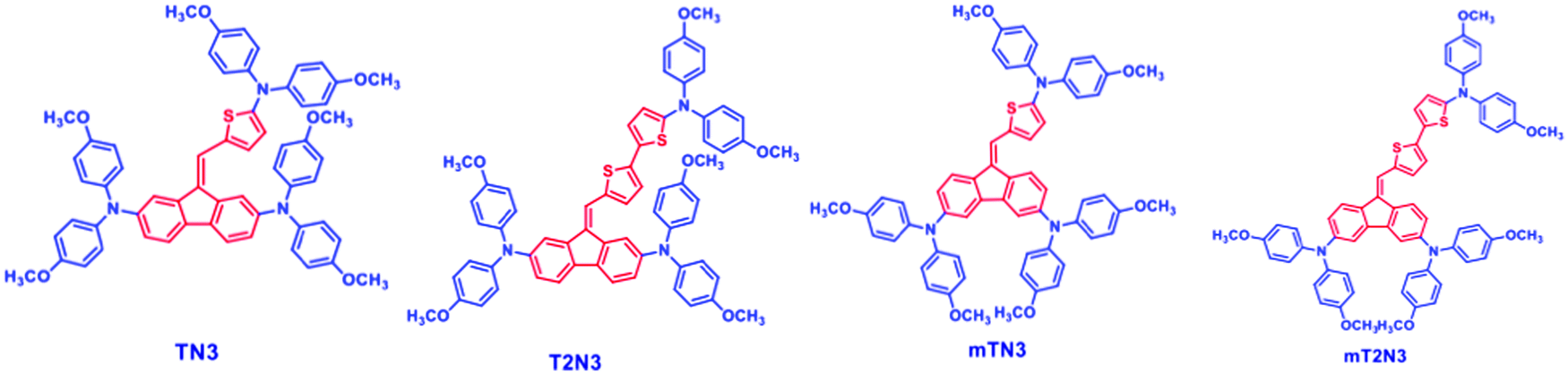 | ||
| Fig. 1 Chemical structure of compounds TN3, T2TN3, mTN3 and mT2N3. | ||
2.2 Electronic properties
A good alignment of the four compounds’ HOMO levels with the valence band of the solar cell absorbing layer, to achieve an efficient hole injection, is one of the fundamental prerequisites to make them suitable HTM candidates. Thus, the HOMO levels of the four materials, including spiro, were estimated using cyclic voltammetry.11 The calculated HOMO energy levels together with the lowest unoccupied molecular orbital (LUMO) values are reported in Fig. 2 (colored box). | ||
| Fig. 2 Energy level diagram, as determined experimentally by cyclic voltammetry, for the HTMs studied in the present work (colored box). | ||
The molecular geometry and electron density distribution were investigated using density functional theory (DFT) calculations.11 The DFT calculations revealed that the main orbital contributions to the HOMO level come from the peripheral arylamino side arms and the DBF bridge for compounds TN3 and T2N3. Meanwhile, it comes mainly from the DBF bridge and the thiophene units in compounds mTN3 and mT2N3, as shown in Fig. 3. From this analysis, a first insight into the carrier–transport properties of the studied compounds can already be obtained. Indeed, more delocalized HOMO orbitals lead to a larger hole transfer integral.
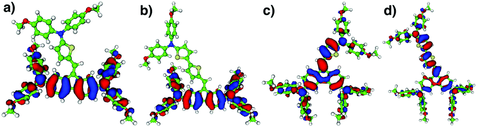 | ||
| Fig. 3 Isodensity plots of the highest occupied molecular orbitals (HOMOs) of (a) TN3, (b) T2N3, (c) mTN3 and (d) mT2N3 extracted from DFT calculations. | ||
2.3 Structural properties
For all of the investigated materials, it was not possible to grow any single-crystal. Thus, grazing incidence wide angle scattering (GIWAXS) experiments were performed on thin films of the new compounds and spiro to gain an insight into their structural properties.20 All GIWAXS patterns were collected with a 0.18° incidence angle, and were characterized by continuous diffraction rings, indicating the random orientation of the molecular domains. In Fig. 4, the 2D- and 1D-folded GIWAXS patterns related to the T2N3 and spiro samples, collected at a 206 mm sample-detector distance, are reported. All other HTM samples considered here exhibited diffraction patterns similar to the T2N3 one, as shown in Fig. S2 (ESI†). A wider diffraction ring is ascribed to the main amorphous fraction in the sample; two (for the new compounds) and one (for spiro) more inner diffraction rings are representative of the nanoscale order and are therefore ascribed to the minority fraction of ordered molecules. | ||
| Fig. 4 2D and 1D-folded GIWAXS patterns from spiro and T2N3 thin films, collected at a 206 mm sample–detector distance. Diffraction rings due to nanoscale periodicities are indicated by arrows, showing two different periodicities for T2N3 (1.60 ± 0.05 nm and 0.94 ± 0.05 nm) and only one periodicity for spiro (1.4 ± 0.05 nm). 2D data are integrated over an 80° azimuthal range in the OFF-specular direction in order to get rid of the sample reflectivity. | ||
It was found that the inner rings are clearly visible in the patterns of the T2N3 and TN3 samples even for a relatively short integration time (∼50 min), indicating a higher degree of nanoscale order in these samples, whereas the rings are hardly visible in mT2N3 and mTN3 (Fig. S2, ESI†). However, it has been verified that, for a much longer integration time (a few hours), very weak similar rings can be recognized in the patterns relevant to the mT2N3 and mTN3 samples (not shown) as well, indicating a similar nanoscale packing for all four molecules considered here. In particular, as shown in Fig. 4, the new compounds are characterized by two distinct repetition distances of 1.60 ± 0.05 and 0.94 ± 0.05 nm, whereas spiro is characterized by a unique repetition distance of 1.40 ± 0.05 nm. This is consistent with the higher isotropic characteristic of the spiro molecule, compared to the other ones that arrange with different packing periodicities along two different axes. Indeed, the 1.4 nm periodicity measured for spiro matches its inter-molecular (center-to-center) distance;21–23 thus, we can argue that the 1.6 and 0.94 nm periodicities found for TN3, T2N3, mTN3, and mT2N3 represent their inter-molecular distances along two packing directions.
2.4 Hole transport properties
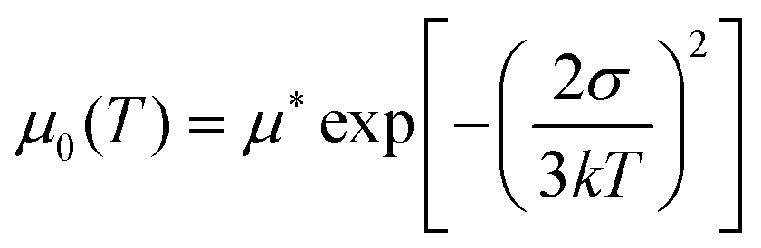
Another important feature of HTMs is their ability to transport charges. We tried to correlate the effect of the difference in the size and shape of our molecules with their electronic transport properties. The charge mobility was studied by performing SCLC measurements,24,25 such as measuring charge transport in the direction perpendicular to the film, which is the direction most relevant for photovoltaic applications or light emitting diodes.26,27 The SCLC technique requires the formation of unipolar-devices characterised by ohmic contacts to pursue a bulk-limited charge transport.28 Eventually, the use of symmetric contacts would be also helpful to avoid any undesired effects due to the presence of a built-in voltage (Fig. S5 and 6, ESI†). For the above reasons, hole-only devices, characterized by ohmic and symmetric contacts, were prepared by spin-casting solutions of TN3, T2N3, mTN3 and mT2N3 onto pre-patterned ITO substrates, with the following stack structure: ITO/PEDOT:PSS/HTM/MoO3/Au. To evaluate the key parameters of charge transport, J–V curves were analysed in terms of the SCLC model, according to the Murgatroyd–Gill (MG) equation:24,29 | (1) |
 | (2) |
 | (3) |
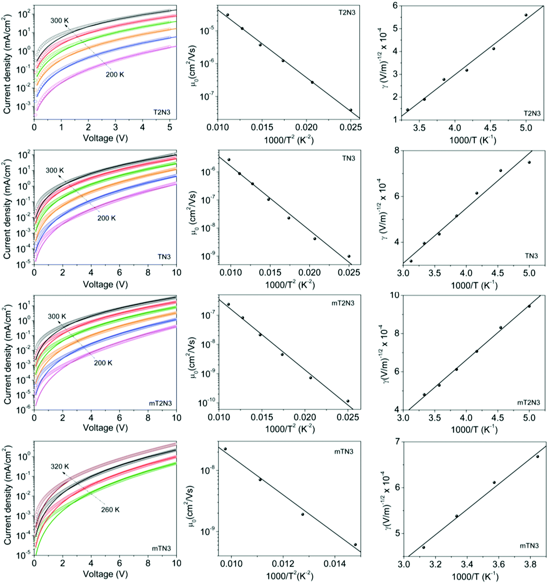 | ||
| Fig. 5 Temperature dependent current–voltage characteristics (left column). The extracted γ values plotted against 1/T (right column) and zero-field mobility against 1/T2 (middle column). Solid lines represent the best fit according to eqn (1)–(3), respectively. All measurements have been performed in a temperature range of 200–300 K with a 20 K step. | ||
We found (Table S1, ESI†) that by changing the anchoring position of arylamines on the DBF core, the mobility increased by two orders of magnitude as we moved from mTN3 and mT2N3 to TN3 and T2N3, respectively. This can be nicely explained by our DFT calculations, which show that, in TN3 and T2N3 (a and b in Fig. 3), the frontier electron density is localized on DBF and the two side arylamino units have an almost uniform distribution, whereas in mTN3 and mT2N3 (c and d in Fig. 3), the reduced coupling of the side groups to DBF, due to the different anchoring positions, reduces the contribution of both arylamino units in favour of a frontier electron distribution localized on DBF and the thiophene units. Hence, in compounds TN3 and T2N3, the larger charge delocalization favours the overlap between the molecular orbitals and thus the electronic coupling, leading to a higher hole mobility.30 We also performed SCLC measurements on spiro to directly compare our compounds with the “benchmark”. We found (Fig. S3a, ESI†) that there is a good match between the J–V characteristics of spiro and T2N3, leading to similar mobility values (3–5 × 10⁻⁵ cm2 V−1 s−1), thus making the latter one a promising candidate for PSCs.
Fig. 5 (left column) shows a deviation of the fit (solid line) from the experimental data (symbols) at low voltages (<2 V). This is due to the analytical modelling procedure (eqn (1)) that does not consider the current diffusion term, which is on the other hand negligible at a larger bias where the drift current dominates. Additionally, we applied drift–diffusion (DD) modelling31 that considers both drift and diffusion terms and it is not constrained to the space-charge-limited region (slope > 2) as eqn (1) and the sub-2 slope of the J–V curves can be reproduced (Fig. 6). All four material fittings were obtained without using any additional trapping parameters. Fig. 6 shows the experimental J–V curves against temperature (symbols), which have been analysed using the DD model parametrized according to the extended-GDM (eGDM) (dashed blue lines)32 and the effective temperature-GDM (ET-GDM) mobility dependence.33,34 The latter model consists of two versions, one calibrated using kinetic Monte Carlo calculations on a regular lattice (solid red lines) and the other on a random lattice instead (dotted black lines). All the above models are integrated in a freeware DD solver.35 The resulting extracted parameters are reported in Tables S2 (ESI†). For all compounds, there is no significant difference in the fit quality (slope > 2) nor in the extracted disorder and zero-field mobility (see Tables S1 and S2, ESI†) between the DD model and the empirical MG equation. Thus, this demonstrates the good reliability of the analytical model, at least in the present case.
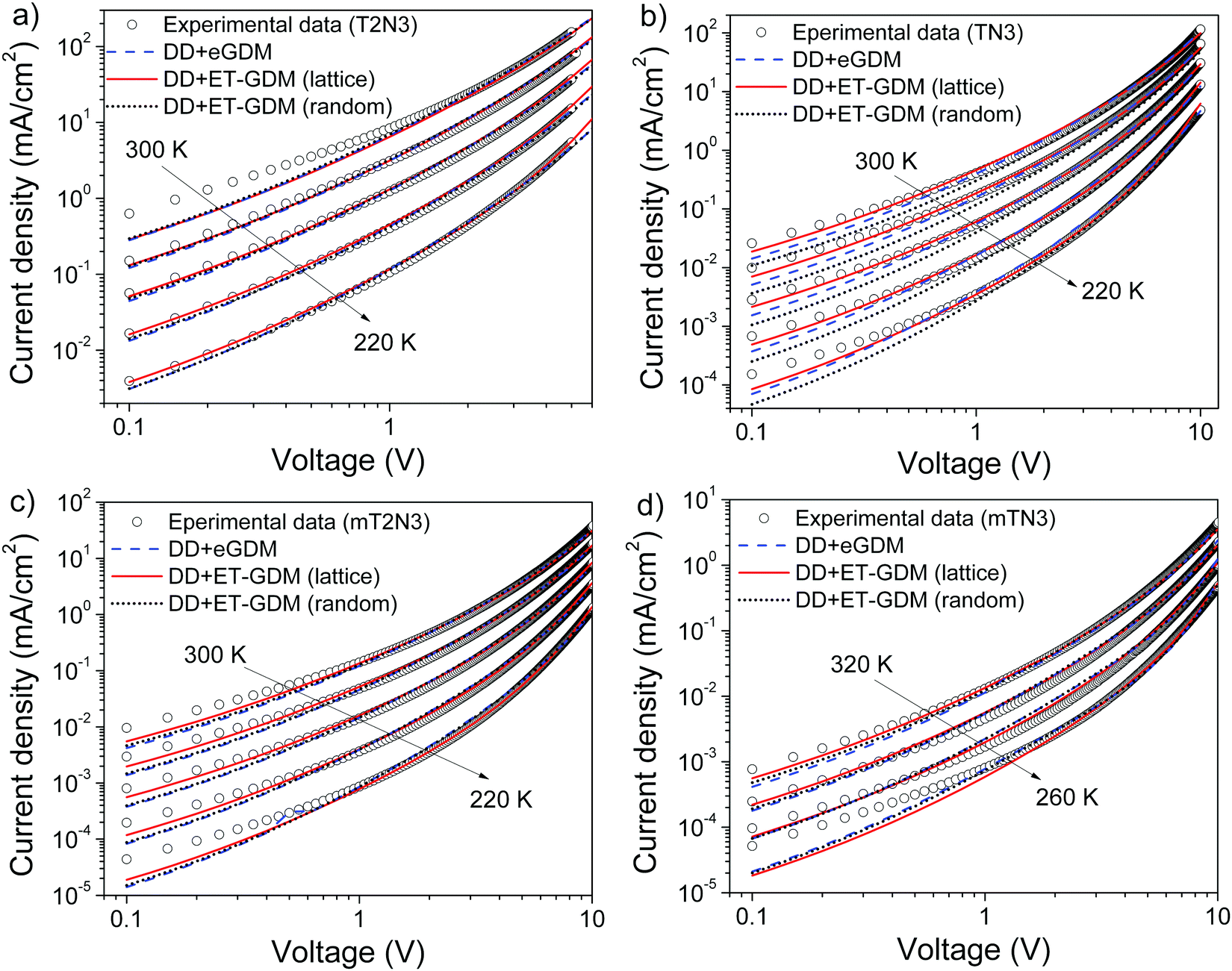 | ||
| Fig. 6 Current density–voltage characteristics at different temperatures for (a) T2N3, (b) TN3, (c) mT2N3, and (d) mTN3. Symbols represent the experimental data and the lines are numerical drift–diffusion model fits with mobilities described using the eGDM (dashed blue lines), lattice ET-GDM (solid red lines) and random ET-GDM (dotted black lines). | ||
Visually, it seems that both the eGDM and ET-GDM fit well the J–V curves; however, it can be seen from Fig. S7 (ESI†) that the ET-GDM (lattice) fits better the slope–voltage characteristics in the whole range of temperatures investigated, but especially in the low range. A possible reason lies in the assumption that, in the eGDM, the charge transport mechanism is based on nearest-neighbour hopping (nnH) on a cubic lattice, i.e. the hopping distance is constant and equal to the nearest-neighbour one, which can be hindered at low temperature. Meanwhile, the ET-GDM accounts for a more realistic “irregular” hopping considering a variable range hopping (VRH).24,31,34 In this latter case, non-neighbour hopping towards more energetically favourable sites is allowed, describing better the scenario of charge transport at low temperatures. Furthermore, the reason behind the better fit of the lattice ET-GDM compared to the random one may be due to the fact that materials might have a significant short-range order, even if a long-range order is absent (amorphous). In other words, the random model will probably overestimate the spatial disorder. This hypothesis is consistent with our GIWAXS patterns that reveal the presence of a short-range order within the investigated materials (see Fig. 4).
Considering the ET-GDM (lattice) as a more appropriate model, the extracted charge localization radius (α) was about 4 Å and the inter-site distance (αNN) was found to be on average around 1.7 nm for compounds mTN3, mT2N3, and TN3 and 1 nm for T2N3 (Table S2, ESI†). The average inter-site distances match well with the two periodicities already found by our GIWAXS measurements. We can suppose that charge transport in compounds mTN3, mT2N3, and TN3 takes place along the ordered structure having a periodicity of 1.6 nm, which forms a percolation path through which the holes move more easily across the amorphous bulk, while in T2N3, the holes move along the direction having a shorter periodicity (1 nm). At present, we do not have enough evidence to clearly identify the reason for the two different hopping paths, as no preferred orientation of the ordered domains can be observed from the GIWAXS patterns. Energy disorder shows also an appreciable variation upon structural modification. The extracted σ value of compound T2N3 is the smallest one, indicating a higher degree of local order within the amorphous phase in this compound. This is consistent with the GIWAXS patterns that are characterized by more intense diffraction peaks for compound T2N3.
2.5 Perovskite solar cell realization and characterization
PSCs with an n–i–p configuration (Fig. 2) were fabricated to investigate the potential of our compounds as HTMs. Solar cell performances, employing T2N3, TN3, mTN3 and spiro as the reference, were measured under AM 1.5G illumination, and the results are displayed through the current density–voltage plots (reverse scans) in Fig. 7a. The sample mT2N3 does not lie in Fig. 7 due to its poor film quality (further details in the ESI†).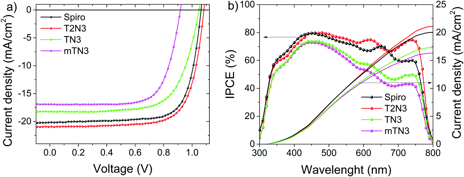 | ||
| Fig. 7 (a) Reverse current–voltage characteristics and (b) incident photon to current conversion efficiency (IPCE) spectra and integrated current densities. | ||
To investigate the reproducibility of our results, statistics of the main solar cell parameters are summarized and presented in Fig. 8. Comparing our newly synthesized materials, the T2N3-based PSCs exhibit the best performances with an average open-circuit voltage (Voc) of (1.08 ± 0.01) V, a short circuit current density (Jsc) of (20.7 ± 0.5) mA, and a fill factor (FF) of (71 ± 2)%, leading to a PCE of (15.8 ± 0.6)%. Such performances also compare well with the reference device based on spiro,36–38 see Table S3 (ESI†). Removing a thiophene ring along the arylamino branched arm, the TN3 based PSC showed a lower PCE (13.5 ± 0.7)%, together with a Voc of (1.01 ± 0.03) V, a Jsc of (19.0 ± 0.9) mA and an FF of (69 ± 2)%. Meanwhile, changing the anchoring position of the arylamine side arms to the DBF core, an obvious decrease of the device performance is observed, and the resulting mTN3 based PSCs showed an efficiency of (11 ± 1)%. A summary of the devices’ average main solar cell parameters is reported in Table S3 (ESI†).
 | ||
| Fig. 8 J SC (a), Voc (b), FF (c), and PCE (d) distributions of PSCs based on different HTMs. | ||
The performances of the PSCs were further confirmed by the incident photon to current conversion efficiency (IPCE) spectra as presented in Fig. 7b. The IPCE spectra of all HTMs exhibit a broad spectral coverage in the entire visible range. Indeed, the integrated photocurrent densities confirm that T2N3 is characterized by a higher current density of 21.6 mA cm−2, compared to 17.3 and 16.3 mA cm−2 for the devices with TN3 and mTN3, respectively. The above values are in good agreement with Jsc determined from the J–V curves.
Furthermore, the film morphology can play a crucial role in current extraction. A smoother HTM surface is beneficial for hole extraction and transport within the films, resulting in better photovoltaic performances. Scanning electron microscopy (SEM) images showed (Fig. 9) that the investigated compounds (including spiro) form a homogenous, uniform and pin-hole free thin film, suggesting a good film coverage of the perovskite layer. These results along with their amorphous nature, see Section 2.3, are all positive findings for the formation of a good HTM/perovskite interface, which is crucial for an efficient charge transfer.17
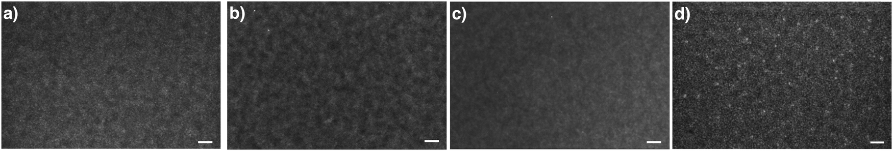 | ||
| Fig. 9 SEM images of (a) spiro, (b) T2N3, (c) TN3, and (d) mTN3 thin films on top of a perovskite layer. Scale bar is 1 μm. | ||
In order to experimentally investigate the efficiency of hole transfer, we performed steady-state photoluminescence (PL) and time-resolved (TRPL) decay measurements. The PL spectra of the neat MAPI film along with spiro, TN3, T2N3, and mTN3 films deposited on top of the perovskite (MAPI/HTMs) are shown in Fig. 10a. It can be seen that there is a strong PL signal at 770 nm from the neat perovskite film, which is severely quenched in the MAPI/HTM samples, indicating an effective hole transfer from the perovskite to the HTMs. The degrees of quenching of all HTMs (including spiro) are quite similar at about 98.5% (estimated by the ratio between area profiles), which is consistent with the decay values shown in Fig. 10b. The average carrier lifetime of the bi-layered samples was obtained using eqn (4) according to the method described by Lakowicz,39
 | (4) |
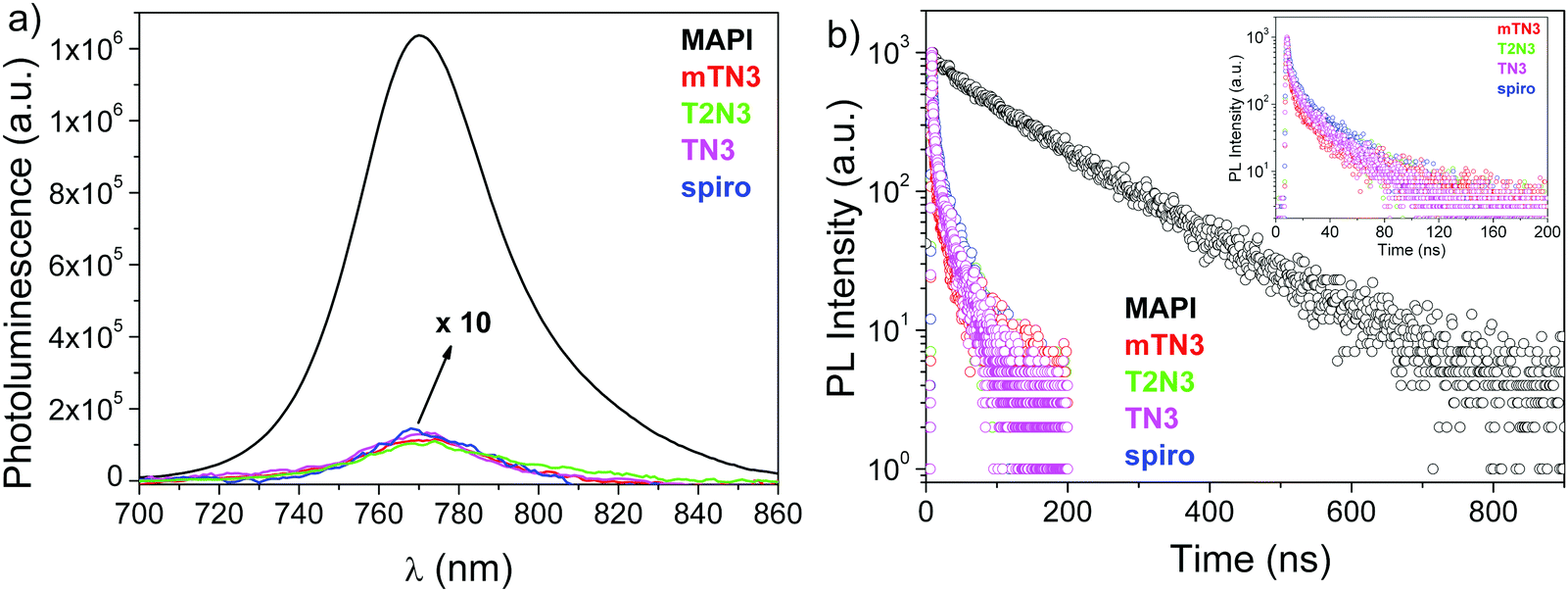 | ||
| Fig. 10 (a) Steady-state PL spectra and (b) time resolved PL decay curves of a pristine MAPI film and of MAPI coated with spiro, T2N3, TN3 and mTN3 on top. | ||
In an n–i–p solar cell configuration, the HTM also plays another important role in protecting the perovskite layer from harmful external factors, such as moisture. Therefore, analysis of the long-term stability of both T2N3- and spiro-based PSCs was performed over 2400 h (100 days). Devices were stored under an ambient atmosphere with a relative humidity (RH) of 50–60% at about 22 °C under dark conditions. The J–V curves of non-encapsulated devices were examined at different time intervals. An initial moderate decrease in solar cell efficiency, as expected for non-encapsulated cells, was shown for both devices (Fig. 11), retaining 80% of their initial value up to 800 h of the aging test. Since then, the efficiency of spiro-based PSCs continuously started to decrease, reaching 30% of its initial value after 1200 h. Meanwhile, the T2N3-based PSCs still continued to maintain 80% of their initial performance up to 2400 h, which is triple the 80% efficiency lifetime of the reference sample. The longer-term stability of T2N3-based PSCs may be attributed to their better hydrophobic nature; indeed, the degradation of spiro-based devices due to moisture has been previously reported.17 It is well-known that hydrophilic dopants in spiro cause moisture-induced degradation pathways, leading to the instability of the devices.40 This is not the case for T2N3-based devices. To understand the reason behind their superior stability, we performed water contact angle measurements of both pristine (undoped) and doped materials. T2N3 and spiro pristine films showed a similar contact angle value of 91° indicating the same degree of hydrophobicity. After doping, it was found that the doping elements have a great impact on the hydrophobicity of spiro, its contact angle value decreased down to 71°, while doping had a negligible effect on T2N3, which showed a water contact angle of 84°, Fig. S9 (ESI†). This result indicates a relatively higher hydrophobicity of T2N3, suggesting a better protection of the HTM/perovskite interface from water ingress, which directly contributes to the improved stability.41,42 We can clearly see, from the optical images of both PSCs (Fig. 11, inset), that before being exposed to the atmosphere, both samples exhibited a shiny brown color. After exposing the sample to ambient conditions, the prominent degradation of the perovskite film in the spiro-based PSC is apparent, and the perovskite film became dull. Meanwhile, only a slight degradation can be observed for the perovskite covered by T2N3.
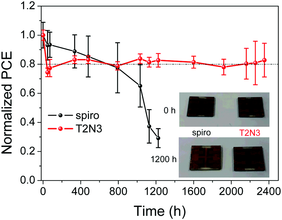 | ||
| Fig. 11 Long-term stabilities of PSCs based on T2N3 (red dots) and spiro (black dots). PSCs were stored under ambient air (22 °C and 50–60% RH) without any encapsulation. The inset shows a picture of both samples at 0 h (fresh) and after 1200 h. | ||
In summary, we used the well-known MAPI as a “prototype” perovskite, although more efficient perovskite absorbing layers have already been reported in the literature,43,44 because HTMs are the focus of this investigation. Keeping this in mind, we demonstrated the potential of T2N3 as a suitable HTM for the realization of PSCs having efficiencies comparable to those of spiro, but with a longer-term stability and a simpler and cheaper synthesis procedure.
3. Conclusions
In conclusion, the electronic structure, the structural and optoelectronic properties of a series of newly synthesized star-shaped organic small molecules have been studied by cyclic voltammetry, DFT calculations, GIWAXS and SCLC measurements, in order to correlate the properties of materials to device performances such as efficiencies and lifetimes.In particular, their ability to transport charges (holes) from the perovskite to the counter electrode was studied by temperature dependent space charge limited current measurements, in combination with analytical and drift–diffusion modelling to extract the charge transport main parameters. From the SCLC analysis, the best compound was found to be T2N3, whose zero-field mobility was similar to that of spiro (3 × 10⁻⁵ cm2 V−1 s−1). Indeed, PSCs based on T2N3 showed efficiencies comparable to that of spiro, but, in addition, T2N3 protected more efficiently the underneath perovskite active layer from environmental agents, leading to a solar cell lifetime triple that of spiro-based PSCs. These results, along with a facile and cheaper synthesis cost, make T2N3 a promising candidate for the large scale production of PSCs.
4. Experimental
Compounds T2N3, TN3, mT2N3 and mTN3 were synthesized according to a previously reported procedure.11Materials
Ultra-dry 99.999% lead(II) iodide (PbI2) (metal basis) was purchased from Alfa Aesar; methylammonium iodide (MAI) was obtained from Greatcell Solar; PEDOT:PSS Al 4083 was supplied from Heraeus; [6,6]-phenyl C61 butyric acid methyl ester (PCBM) was purchased from Nano-c; tin(IV) oxide 15 wt% colloidal solution was purchased from Alfa Aesar; bis(trifluoromethane)sulfonimide lithium salt (Li-TFSI), 4-tert-butylpyridine (tBP), and MoO3 powder were from Sigma Aldrich.UV-vis absorption spectra were recorded using a Varian Cary 3000 spectrophotometer.
The electrochemical characterization of the compounds was carried out by cyclic voltammetry (CV) using an Autolab (Metrhom Mod.) potentiostat. A typical three-electrode cell was assembled with a glassy carbon disk-working electrode, a Pt wire auxiliary electrode, and an Ag/AgCl nonaqueous reference electrode. Cyclic voltammograms were acquired at 50 mV s−1 in 1 mM compound solutions prepared in an electrolyte solution, consisting of 0.1 M tetrabutylammonium hexafluorophosphate (TBAPF6) in dichloromethane (CH2Cl2). All of the solutions were previously degassed with N2. The CV curves of the ferrocenium/ferrocene (Fc+/Fc) couple (1 mM) were recorded under the same conditions as those of all of the other compound solutions and used as the external reference for potential calibration.
DFT computations
All calculations were performed using the TURBOMOLE45,46 program with the PBE0-1/3 functional47 and a def2-TZVP basis set.48GIWAXS measurements
GIWAXS data were collected using a Rigaku (GI)SAXS/(GI)WAXS instrument equipped with an FR-E+ superbright rotating anode microscource (Cu Kα, λ = 1.5405 Å) coupled to a three-pinhole camera through a Confocal Max Flux optics.49 An image plate detector with offline readout (RAXIA) was employed at a sample-to-detector distance (SDD) of 87 mm or 206 mm, as specified in the text. Data were calibrated by using Si (NIST) or Ag-Behenate standard powders. The pressures in the sample chamber and flight tube were kept at ∼5 × 10⁻² mbar. The incidence angle was fixed at αi = 0.18° for all samples, in order to eliminate substrate scattering. Correction for geometric projection on a flat detector (for the shorter SDD) was performed using the in-house developed SUNBIM freeware program suite.50SEM characterization
Morphological SEM characterization was performed using a ZEISS Sigma 300 field emission SEM (FE-SEM) instrument in high vacuum and high-resolution mode, equipped with a Gemini column and an integrated high efficiency in-lens detector. A 5 kV voltage acceleration was used.Solar cell realization and characterization
The MAPI solution was prepared according to the literature51 by solubilizing an equimolar stoichiometry, i.e. MAI![[thin space (1/6-em)]](https://www.rsc.org/images/entities/char_2009.gif) :PbI2:DMSO = 1:1:1, in DMF (precursor concentration 48 wt%). Spiro-OMETAD (70 mM) and HTM compound (25 mM) solutions were prepared by dissolving in chlorobenzene along with tBP, and Li-TFSI in acetonitrile (520 mg ml−1), at a molar ratio of 1:0.5:3.3 (Spiro/HTMs:Li-TFSI:tBP). The solutions were prepared inside an N2 filled glove box. The n–i–p solar cells were realized as follows: glass/ITO/SnO2/PCBM/MAPI/HTM/MoO3/Au. ITO coated glass substrates were cleaned by ultrasonication in acetone and 2-propanol, and then underwent oxygen plasma treatment. SnO2, 2.5 wt% colloidal solution in water, was deposited on top of ITO by spin coating at 4000 rpm for 60 s and annealed at 150 °C for 30 min in air. PCBM (10 mg ml−1 in chlorobenzene) was then deposited on top at 2000 rpm for 30 s and annealed at 100 °C for 20 min in a glove box. Subsequently, the MAPI was spin coated on top of the PCBM at 4000 rpm for 25 s and 10 s before finally 200 μL of toluene was dropped on the films and annealed at 100 °C for 10 min. Our HTMs, including spiro, were sequentially deposited onto the active layer at 4000 rpm for 20 s. Finally, thin films of MoO3 (10 nm) and Au (80 nm) were deposited through a shadow mask by high vacuum thermal evaporation, defining an active area of about 0.04 cm2.
:PbI2:DMSO = 1:1:1, in DMF (precursor concentration 48 wt%). Spiro-OMETAD (70 mM) and HTM compound (25 mM) solutions were prepared by dissolving in chlorobenzene along with tBP, and Li-TFSI in acetonitrile (520 mg ml−1), at a molar ratio of 1:0.5:3.3 (Spiro/HTMs:Li-TFSI:tBP). The solutions were prepared inside an N2 filled glove box. The n–i–p solar cells were realized as follows: glass/ITO/SnO2/PCBM/MAPI/HTM/MoO3/Au. ITO coated glass substrates were cleaned by ultrasonication in acetone and 2-propanol, and then underwent oxygen plasma treatment. SnO2, 2.5 wt% colloidal solution in water, was deposited on top of ITO by spin coating at 4000 rpm for 60 s and annealed at 150 °C for 30 min in air. PCBM (10 mg ml−1 in chlorobenzene) was then deposited on top at 2000 rpm for 30 s and annealed at 100 °C for 20 min in a glove box. Subsequently, the MAPI was spin coated on top of the PCBM at 4000 rpm for 25 s and 10 s before finally 200 μL of toluene was dropped on the films and annealed at 100 °C for 10 min. Our HTMs, including spiro, were sequentially deposited onto the active layer at 4000 rpm for 20 s. Finally, thin films of MoO3 (10 nm) and Au (80 nm) were deposited through a shadow mask by high vacuum thermal evaporation, defining an active area of about 0.04 cm2.
Solar cells were characterized in air, under the standard conditions of light intensity (100 mW cm−2, AM1.5) using a solar simulator (Newport 91160A) and a source measurement unit (Keithely 2400). The current–voltage characteristics of the devices were acquired in the voltage range of −0.2 to 1.2 V. The IPCE was measured in air using a power source (Newport xenon lamp, 140 W, 67005) coupled with a monochromator (Newport Cornerstore 260 Oriel 74125), a photodiode (Newport Oriel 71675_71580) and a dual channel optical power/energy meter (Newport 2936-C).
SCLC device realization and characterization
Devices for SCLC measurements were realized as follows: glass/ITO/Pedot:PSS/HTM/MoO3/Au. The substrate cleaning process was the same as that reported above. PEDOT:PSS was filtered using a 0.45 μm PVDF syringe filter, and then it was spun onto ITO at 4000 rpm for 60 s and annealed at 140 °C for 20 min in air. Then, the substrates were loaded inside a glove box, and spiro or our HTMs, dissolved in chlorobenzene at a concentration of 70 mg mL−1, were spun at 2000 rpm for 20 s. Finally, a MoO3/Au metal contact was deposited through a shadow mask by high vacuum thermal evaporation, defining an active area of about 0.04 cm2. The devices were characterized within a sample stage (Linkam LTS420E-P) under dynamic vacuum. The temperature was varied between 300 and 220 K while the current–voltage characteristics were recorded using a computer controlled pico-ammeter (HP 4140B).Spectroscopic measurements
Uncorrected emission spectra were recorded using an Edinburgh FLS980 spectrometer equipped with a peltier-cooled Hamamatsu R928 photomultiplier tube (185–850 nm). An Edinburgh Xe900 450 W xenon arc lamp was used as the exciting light source. Corrected spectra were obtained via a calibration curve supplied with the instrument. Emission lifetimes in the ps–μs range were determined with the single photon counting technique by means of the same Edinburgh FLS980 spectrometer using a laser diode as the excitation source (1 MHz, λexc = 407 nm) and a Hamamatsu MCP R3809U-50 (time resolution 20 ps) as the detector. Experimental uncertainties are estimated to be ±8% for lifetime determinations and ±5 nm for emission peaks.Conflicts of interest
There are no conflicts to declare.Acknowledgements
The authors gratefully thank Sonia Carallo for technical support and Elisabetta Perrone for performing contact angle measurements. S. G. would like to thank Prof. Martijn Kemerink (Centre for Advanced Materials, Ruprecht-Karls-Universität Heidelberg, Germany) for useful discussions about SCLC data analysis. This work was supported by “Tecnopolo per la medicina di precisione” (TecnoMed Puglia) —Regione Puglia: DGR n.2117 del 21/11/2018, CUP: B84I18000540002 and “Tecnopolo di Nanotecnologia e Fotonica per la medicina di precisione” (TECNOMED)—FISR/MIUR-CNR: delibera CIPE n.3449 del 7-08-2017, CUP: B83B17000010001, funded by the Italian Ministry of University and Scientific Research (MIUR) and Regione Puglia. A.R. gratefully acknowledges the project Best4U – “Tecnologia per celle solari bifacciali ad alta Efficienza a 4 terminali per utility scale” funded by the Italian Ministry of University ad Scientific Research (MIUR), Bando PON R&I 2014-2020 e FSC “Avviso per la presentazione di Progetti di Ricerca Industriale e Sviluppo Sperimentale nelle 12 aree di Specializzazione individuate dal PNR 2015-2020” – decreto concessione agevolazione protocollo 991 del 21 maggio 2019 MIUR (contract number: PON ARS01_00519; CUP B88D19000160005).References
- Spiro-MeOTAD 99% (HPLC) | 207739-72-8 [Internet]. [cited 2021 Sep 14], available from: https://www.sigmaaldrich.com/IT/it/product/aldrich/792071.
- T. Niu, W. Zhu, Y. Zhang, Q. Xue, X. Jiao and Z. Wang, et al., D–A–π–A–D-type dopant-free hole transport material for low-cost, efficient, and stable perovskite solar cells, Joule, 2021, 5(1), 249–269, DOI:10.1016/j.joule.2020.12.003.
- H. Tang, C. Yan, J. Huang, Z. Kan, Z. Xiao and K. Sun, et al., Benzodithiophene-based small-molecule donors for next-generation all-small-molecule organic photovoltaics, Matter, 2020, 3(5), 1403–1432, DOI:10.1016/j.matt.2020.09.001.
- K. Rakstys, C. Igci and M. K. Nazeeruddin, Efficiency vs. stability: Dopant-free hole transporting materials towards stabilized perovskite solar cells, Chem. Sci., 2019, 10(28), 6748–6769 RSC , available from: http://xlink.rsc.org/?DOI=C9SC01184F.
- C. Rodríguez-Seco, M. Méndez, C. Roldán-Carmona, L. Cabau, A. M. Asiri and M. K. Nazeeruddin, et al., Benzothiadiazole aryl-amine based materials as efficient hole carriers in perovskite solar cells, ACS Appl. Mater. Interfaces, 2020, 12(29), 32712–32718, DOI:10.1021/acsami.0c07586.
- T. Malinauskas, M. Saliba, T. Matsui, M. Daskeviciene, S. Urnikaite and P. Gratia, et al., Branched methoxydiphenylamine-substituted fluorene derivatives as hole transporting materials for high-performance perovskite solar cells, Energy Environ. Sci., 2016, 9(5), 1681–1686 RSC , available from: http://xlink.rsc.org/?DOI=C5EE03911H.
- Š. Daškevičiūtė, N. Sakai, M. Franckevičius, M. Daškevičienė, A. Magomedov and V. Jankauskas, et al., Nonspiro, fluorene-based, amorphous hole transporting materials for efficient and stable perovskite solar cells, Adv. Sci., 2018, 5(4), 1700811, DOI:10.1002/advs.201700811.
- A. A. Sutanto, V. Joseph, C. Igci, O. A. Syzgantseva, M. A. Syzgantseva and V. Jankauskas, et al., Isomeric carbazole-based hole-transporting materials: Role of the linkage position on the photovoltaic performance of perovskite solar cells, Chem. Mater., 2021, 33(9), 3286–3296, DOI:10.1021/acs.chemmater.1c00335.
- J.-Y. Shao and Y.-W. Zhong, Design of small molecular hole-transporting materials for stable and high-performance perovskite solar cells, Chem. Phys. Rev., 2021, 2(2), 021302, DOI:10.1063/5.0051254.
- R. Iacobellis, S. Masi, A. Rizzo, R. Grisorio, M. Ambrico and S. Colella, et al., Addressing the function of easily synthesized hole transporters in direct and inverted perovskite solar cells, ACS Appl. Energy Mater., 2018, 1(3), 1069–1076, DOI:10.1021/acsaem.7b00208.
- A.-L. Capodilupo, E. Fabiano, L. Franco, S. Gambino, M. Leoncini and G. Accorsi, et al., Control of electron transfer processes in multidimensional arylamine-based mixed-valence compounds by molecular backbone design, J. Phys. Chem. A, 2021, 125(36), 7840–7851, DOI:10.1021/acs.jpca.1c05435.
- M. Kuik, G.-J. J. A. H. Wetzelaer, H. T. Nicolai, N. I. Craciun, D. M. De Leeuw and P. W. M. Blom, 25th anniversary article: Charge transport and recombination in polymer light-emitting diodes, Adv. Mater., 2014, 26(4), 512–531 CrossRef CAS PubMed , available from: http://www.advmat.de.
- Y. Sun, T. Liu, Y. Kan, K. Gao, B. Tang and Y. Li, Flexible organic solar cells: Progress and challenges, Small Sci., 2021, 1(5), 2100001, DOI:10.1002/smsc.202100001.
- R. Ma, K. Zhou, Y. Sun, T. Liu, Y. Kan and Y. Xiao, et al., Achieving high efficiency and well-kept ductility in ternary all-polymer organic photovoltaic blends thanks to two well miscible donors, Matter, 2022, 5(2), 725–734, DOI:10.1016/j.matt.2021.12.002.
- M. Leoncini, R. Giannuzzi, A. Giuri, S. Colella, A. Listorti and V. Maiorano, et al., Electronic transport, ionic activation energy and trapping phenomena in a polymer-hybrid halide perovskite composite, J. Sci. Adv. Mater. Devices, 2021, 6(4), 543–550 CrossRef CAS , available from: https://linkinghub.elsevier.com/retrieve/pii/S2468217921000575.
- F. Bisconti, A. Giuri, R. Suhonen, T. M. Kraft, M. Ylikunnari and V. Holappa, et al., One-step polymer assisted roll-to-roll gravure-printed perovskite solar cells without using anti-solvent bathing, Cell Rep. Phys. Sci., 2021, 2(11), 100639, DOI:10.1016/j.xcrp.2021.100639.
- Y.-D. Lin, K.-M. Lee, S. H. Chang, T.-Y. Tsai, H.-C. Chung and C.-C. Chou, et al., Molecularly engineered cyclopenta[2,1-b;3,4-b′]dithiophene-based hole-transporting materials for high-performance perovskite solar cells with efficiency over 19%, ACS Appl. Energy Mater., 2021, 4(5), 4719–4728, DOI:10.1021/acsaem.1c00328.
- J. Zhang, B. Xu, L. Yang, C. Ruan, L. Wang and P. Liu, et al., The importance of pendant groups on triphenylamine-based hole transport materials for obtaining perovskite solar cells with over 20% efficiency, Adv. Energy Mater., 2018, 8(2), 1701209, DOI:10.1002/aenm.201701209.
- G. Mallesham, C. Swetha, S. Niveditha, M. E. Mohanty, N. J. Babu and A. Kumar, et al., Phosphine oxide functionalized pyrenes as efficient blue light emitting multifunctional materials for organic light emitting diodes, J. Mater. Chem. C, 2015, 3(6), 1208–1224, 10.1039/C4TC01753F.
- Z. Wang, K. Gao, Y. Kan, M. Zhang, C. Qiu and L. Zhu, et al., The coupling and competition of crystallization and phase separation, correlating thermodynamics and kinetics in OPV morphology and performances, Nat. Commun., 2021, 12(1), 332, DOI:10.1038/s41467-020-20515-3.
- Y. Li, H. Li, C. Zhong, G. Sini and J.-L. Brédas, Characterization of intrinsic hole transport in single-crystal spiro-OMeTAD, npj Flex Electron., 2017, 1(1), 2, DOI:10.1038/s41528-017-0002-0.
- P. Ganesan, K. Fu, P. Gao, I. Raabe, K. Schenk and R. Scopelliti, et al., A simple spiro-type hole transporting material for efficient perovskite solar cells, Energy Environ. Sci., 2015, 8(7), 1986–1991, 10.1039/C4EE03773A.
- N. B. Kotadiya, A. Mondal, S. Xiong, P. W. M. Blom, D. Andrienko and G. A. H. Wetzelaer, Rigorous characterization and predictive modeling of hole transport in amorphous organic semiconductors, Adv. Electron Mater., 2018, 4(12), 1800366, DOI:10.1002/aelm.201800366.
- N. Felekidis, A. Melianas and M. Kemerink, Automated open-source software for charge transport analysis in single-carrier organic semiconductor diodes, Org. Electron., 2018, 61, 318–328 CrossRef CAS , available from: https://linkinghub.elsevier.com/retrieve/pii/S156611991830301X.
- M. Nikolka, K. Broch, J. Armitage, D. Hanifi, P. J. Nowack and D. Venkateshvaran, et al., High-mobility, trap-free charge transport in conjugated polymer diodes, Nat. Commun., 2019, 10(1), 2122 CrossRef PubMed , available from: http://www.nature.com/articles/s41467-019-10188-y.
- I a. Wright, P. J. Skabara, J. C. Forgie, A. L. Kanibolotsky, B. González and S. J. Coles, et al., Electronic, redox and charge transport properties of an unusual hybrid structure: A bis(septithiophene) bridged by a fused tetrathiafulvalene (TTF), J. Mater. Chem., 2011, 21(5), 1462 RSC , available from: http://xlink.rsc.org/?DOI=c0jm02293d.
- S. Gambino, S.-C. Lo, Z. Liu, P. L. Burn and I. D. W. Samuel, Charge transport in a highly phosphorescent iridium(III) complex-cored dendrimer with double dendrons, Adv. Funct. Mater., 2012, 22(1), 157–165, DOI:10.1002/adfm.201101727.
- J. A. Röhr, D. Moia, S. A. Haque, T. Kirchartz and J. Nelson, Exploring the validity and limitations of the Mott–Gurney law for charge-carrier mobility determination of semiconducting thin-films, J. Phys.: Condens. Matter, 2018, 30(10), 1–13, DOI:10.1088/1361-648X/aaabad.
- P. N. Murgatroyd, Theory of space-charge-limited current enhanced by Frenkel effect, J. Phys. D: Appl. Phys., 1970, 3(2), 308 CrossRef , available from: http://stacks.iop.org/0022-3727/3/i=2/a=308?key=crossref.80ae82ee2628e4b26b9db6a9a43f9049.
- D. Alberga, G. F. Mangiatordi, F. Labat, I. Ciofini, O. Nicolotti and G. Lattanzi, et al., Theoretical investigation of hole transporter materials for energy devices, J. Phys. Chem. C, 2015, 119(42), 23890–23898, DOI:10.1021/acs.jpcc.5b08981.
- T. Upreti, Y. Wang, H. Zhang, D. Scheunemann, F. Gao and M. Kemerink, Experimentally validated hopping-transport model for energetically disordered organic semiconductors, Phys. Rev. Appl., 2019, 12(6), 064039, DOI:10.1103/PhysRevApplied.12.064039.
- W. F. Pasveer, J. Cottaar, C. Tanase, R. Coehoorn, P. A. Bobbert and P. W. M. Blom, et al., Unified description of charge-carrier mobilities in disordered semiconducting polymers, Phys. Rev. Lett., 2005, 94, 20, DOI:10.1103/PhysRevLett.94.206601.
- S. Marianer and B. I. Shklovskii, Effective temperature of hopping electrons in a strong electric field, Phys. Rev. B: Condens. Matter Mater. Phys., 1992, 46(20), 13100–13103, DOI:10.1103/PhysRevB.46.13100.
- J. O. Oelerich, A. V. Nenashev, A. V. Dvurechenskii, F. Gebhard and S. D. Baranovskii, Field dependence of hopping mobility: Lattice models against spatial disorder, Phys. Rev. B, 2017, 96(19), 195208, DOI:10.1103/PhysRevB.96.195208.
- GitHub – mkemerink/FitSCLC: Automated open-source model for reliable charge transport analysis in organic semiconductor diodes. [cited 2021 Nov 13], available from: https://github.com/mkemerink/FitSCLC.
- R. Azmi, S. Y. Nam, S. Sinaga, Z. A. Akbar, C.-L. Lee and S. C. Yoon, et al., High-performance dopant-free conjugated small molecule-based hole-transport materials for perovskite solar cells, Nano Energy, 2018, 44, 191–198, DOI:10.1016/j.nanoen.2017.12.002.
- J. Yan, Z. Lin, Q. Cai, X. Wen and C. Mu, Choline chloride-modified SnO2 achieving high output voltage in MAPbI3 perovskite solar cells, ACS Appl. Energy Mater., 2020, 3(4), 3504–3511, DOI:10.1021/acsaem.0c00038.
- Y.-D. Lin, K.-M. Lee, B.-Y. Ke, K.-S. Chen, H.-C. Cheng and W.-J. Lin, et al., Rational design of cyclopenta[2,1-b;3,4-b′]dithiophene-bridged hole transporting materials for highly efficient and stable perovskite solar cells, Energy Technol., 2019, 7(2), 307–316, DOI:10.1002/ente.201800939.
- J. R. Lakowicz, Principles of fluorescence spectroscopy, Princ. Fluoresc. Spectrosc., 2006, 1–954 Search PubMed.
- Z. Deng, M. He, Y. Zhang, F. Ullah, K. Ding and J. Liang, et al., Design of low crystallinity spiro-typed hole transporting material for planar perovskite solar cells to achieve 21.76% efficiency, Chem. Mater., 2021, 33(1), 285–297, DOI:10.1021/acs.chemmater.0c03772.
- D. Vaitukaityte, Z. Wang, T. Malinauskas, A. Magomedov, G. Bubniene and V. Jankauskas, et al., Efficient and stable perovskite solar cells using low-cost aniline-based enamine hole-transporting materials, Adv. Mater., 2018, 30(45), 1803735, DOI:10.1002/adma.201803735.
- X. Zhu, X. Ma, Y. Wang, Y. Li, C. Gao and Z. Wang, et al., Hole-transporting materials incorporating carbazole into spiro-core for highly efficient perovskite solar cells, Adv. Funct. Mater., 2018, 29(5), 1807094, DOI:10.1002/adfm.201807094.
- C. Shen, Y. Wu, H. Zhang, E. Li, W. Zhang and X. Xu, et al., Semi-locked tetrathienylethene as a building block for hole-transporting materials: Toward efficient and stable perovskite solar cells, Angew Chem., Int. Ed., 2019, 58(12), 3784–3789, DOI:10.1002/anie.201811593.
- J. Zhou, X. Yin, Z. Dong, A. Ali, Z. Song and N. Shrestha, et al., Dithieno[3,2-b:2′,3′-d]pyrrole cored p-type semiconductors enabling 20% efficiency dopant-free perovskite solar cells, Angew. Chem., Int. Ed., 2019, 58(39), 13717–13721, DOI:10.1002/anie.201905624.
- TURBOMOLE | Program Package for Electronic Structure Calculations [Internet]. [cited 2021 Nov 6], available from: https://www.turbomole.org/.
- F. Furche, R. Ahlrichs, C. Hättig, W. Klopper, M. Sierka and F. Weigend, Turbomole, Wiley Interdiscip. Rev.: Comput. Mol. Sci., 2014, 4(2), 91–100, DOI:10.1002/wcms.1162.
- C. A. Guido, E. Brémond, C. Adamo and P. Cortona, Communication: One third: A new recipe for the PBE0 paradigm, J. Chem. Phys., 2013, 138(2), 021104, DOI:10.1063/1.4775591.
- F. Weigend, M. Häser, H. Patzelt and R. Ahlrichs, RI-MP2: Optimized auxiliary basis sets and demonstration of efficiency, Chem. Phys. Lett., 1998, 294(1–3), 143–152, DOI:10.1016/S0009-2614(98)00862-8.
- D. Altamura, R. Lassandro, F. A. Vittoria, L. De Caro, D. Siliqi and M. Ladisa, et al., X-ray microimaging laboratory (XMI-LAB), J. Appl. Crystallogr., 2012, 45(4), 869–873 CrossRef CAS , available from: http://scripts.iucr.org/cgi-bin/paper?rg5012.
- D. Siliqi, L. De Caro, M. Ladisa, F. Scattarella, A. Mazzone and D. Altamura, et al., SUNBIM: A package for X-ray imaging of nano- and biomaterials using SAXS, WAXS, GISAXS and GIWAXS techniques, J. Appl. Crystallogr., 2016, 49(3), 1107–1114 CrossRef CAS , available from: http://scripts.iucr.org/cgi-bin/paper?vg5039.
- N. Ahn, D. Y. Son, I. H. Jang, S. M. Kang, M. Choi and N. G. Park, Highly reproducible perovskite solar cells with average efficiency of 18.3% and best efficiency of 19.7% fabricated via lewis base adduct of lead(II) iodide, J. Am. Chem. Soc., 2015, 137(27), 8696–8699, DOI:10.1021/jacs.5b04930.
Footnote |
| † Electronic supplementary information (ESI) available. See DOI: 10.1039/d1tc05690e |
| This journal is © The Royal Society of Chemistry 2022 |