
 Open Access Article
 This Open Access Article is licensed under a Creative Commons Attribution-Non Commercial 3.0 Unported Licence
Engineering the sign of circularly polarized emission in achiral polymer – chiral small molecule blends as a function of blend ratio†‡
Li
Wan§¶
 abc,
Jessica
Wade§
abc,
Xuhua
Wang
ac,
Alasdair J.
Campbell||
ac and
Matthew J.
Fuchter
*bc
abc,
Jessica
Wade§
abc,
Xuhua
Wang
ac,
Alasdair J.
Campbell||
ac and
Matthew J.
Fuchter
*bc
aDepartment of Physics, Imperial College London, South Kensington Campus, London SW7 2AZ, UK
bDepartment of Chemistry and Molecular Sciences Research Hub, Imperial College London, White City Campus, 82 Wood Lane, London W12 0BZ, UK. E-mail: m.fuchter@imperial.ac.uk
cCentre for Processable Electronics, Imperial College London, South Kensington Campus, London SW7 2AZ, UK
First published on 25th February 2022
Abstract
Circularly polarized organic light-emitting diodes (CP-OLEDs) that demonstrate both state-of-the-art efficiency and strongly circularly polarized (CP) electroluminescence have proved a considerable technical challenge. Furthermore, multiple factors – from film thickness to device structure – have been shown to influence the sign of the emitted CP light, independent of the handedness (absolute stereochemistry) of the chiral emitter. Here we report CP-OLEDs using a blend of poly(9,9-dioctylfluorene-alt-bithiophene) (F8T2) and a chiral small molecule additive (1-aza[6]helicene, aza[6]H). We demonstrate CP-OLEDs with an impressive electroluminescence dissymmetry (gEL) > 0.3 and a current efficiency of 0.53 cd A−1 and brightness of 3023 cd m−2. While at low aza[6]H loadings, F8T2 blends are consistent with previous observations of CP dissymetric inversion as a function of film thickness/excitation mode, a higher loading of aza[6]H (∼40 wt%) removes such dependencies while retaining excellent g-factors. The materials disclosed will allow for further mechanistic studies of chiral polymeric materials and provide new opportunities for chiroptical optimisation in films and devices.
Introduction
The use of chiral organic semiconductors in optoelectronic devices has attracted considerable scientific interest. One reason for this is the potential to improve the energy efficiency of organic light emitting diodes (OLEDs): the direct emission of CP luminescence from the active layers of OLEDs could significantly reduce optical losses caused by the anti-glare filters used in state-of-the-art displays.1 A key figure of merit for CP-OLEDs is the degree of CP luminescence, which can be defined by the dissymmetry or g-factor (eqn (1)).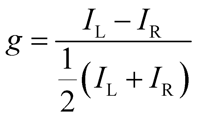 | (1) |
In the pursuit of large g-factors and high quantum efficiencies, a wide range of CP emissive materials have been explored, including light-emitting polymers (LEPs), phosphorescent metal complexes, thermally activated delayed fluorescent (TADF) emitters and perovskites.2 Although triplet-harvesting TADF and phosphorescent emitters can achieve high device efficiencies, the luminescence g-factors are generally negligible (g ≈ 10−2–10−4).3–5 On the other hand, LEPs display large g-factors (e.g. g ≈ 1.0), and the potential to optimise device performance through device engineering and molecular design. The majority of reported chiral LEPs can be categorized into two groups: (1) LEPs with chiral side chains;6,7 and (2) blend systems consisting of device-optimized achiral LEPs and non-emissive chiral small molecule additives.8–11 Our previous studies have demonstrated that such LEPs have very large intrinsic chiroptical activity without the need for polymer alignment, partly due to the formation of chiral polymer phases with large inter-chain excitonic coupling.8,10,12
To date, much of our work on achiral LEPs with chiral additives has concerned the use of poly(9,9-dioctylfluorene-alt-benzothiadiazole) (F8BT) blended with 1-aza[6]helicene (hereafter, aza[6]H). Through rigorous studies of this key blend system, we have discovered a number of interesting trends with respect to the sign of the emitted CP light relative to the handedness/absolute stereochemistry of the chiral active layer. These include luminescence dissymmetry factors that depend on film thickness,13 device architecture,8 and whether the CP emission is photo- or electro-luminescence. However, one parameter that has not been well explored is the influence of the LEP and chiral small molecule additive blend ratio and the effect that such a ratio has on chiroptical activity and device performance.
In this study, we focus on an alternative polymer: poly(9,9-dioctylfluorene-alt-bithiophene) (F8T2, Fig. 1a), an archetypal semiconducting polymer that has been extensively studied as the (non-chiral) active layer in OLEDs,14 organic field-effect transistors,15 and organic solar cells.16 In separate work, it has been demonstrated that, in enantiopure chiral solvents, F8T2 can form helical π–π aggregates which exhibit circular dichroism (CD) and CP photoluminescence (CP PL) (∣gabs∣ ≈ 0.1, ∣gPL∣≈ 0.065).17,18 Here we show that F8T2:aza[6]H blends can be used as the active layer in CP-OLEDs and allow for the observation of fascinating dependencies in the gPL and gEL data on blend ratio. In contrast to the polymeric systems we have previously studied, F8T2:[P]/[M]-aza[6]H blends can tolerate a much higher aza[6]H loading, due to the similar HOMO levels of the two materials (∼ 5.4 eV).19 Enabled by this potential for increased aza[6]H loading, we find that the sign of CP luminescence depends not only on active layer thickness, but also on the wt% of aza[6]H. These intriguing results further highlight the fascinating chiroptical phenomena at play in achiral LEP – chiral additive blends and expands the repertoire of polymers compatible with this approach for effective polymer CP-OLEDs.
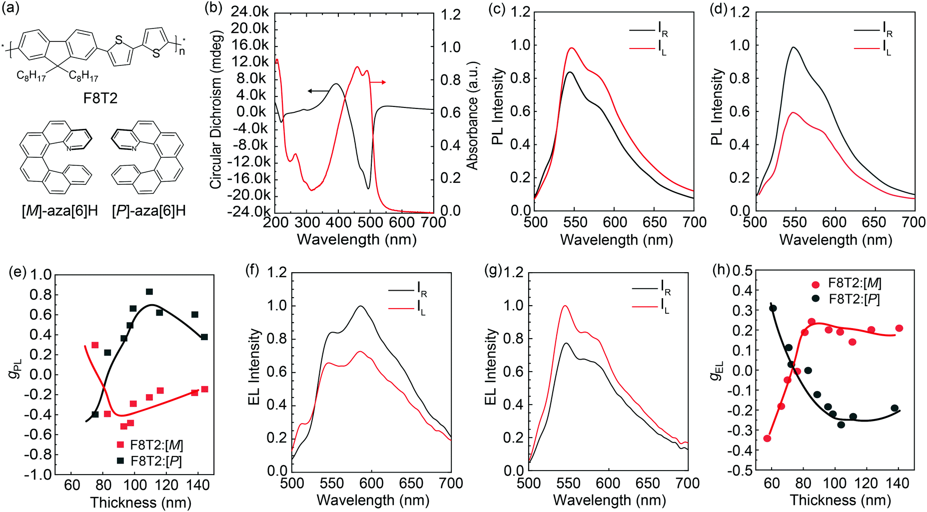 | ||
| Fig. 1 (a) Molecular structures of F8T2 and [M]/[P]-aza[6]H; (b) Circular dichroism spectra and absorption spectra of 100 nm F8T2:10 wt% [M]-aza[6]H film; CP PL of (c) 72 nm and (d) 100 nm F8T2:10 wt% [M]-aza[6]H films; (e) gPL of the F8T2:10 wt% [M]-aza[6]H film as a function of film thickness; CP EL of F8T2:10 wt% [M]-aza[6]H OLEDs with an active layer thickness of (f) 58 nm and (g) 100 nm; (h) gEL as a function of film thickness. OLED device structure: ITO/PEDOT:PSS/TFB/F8T2:10 wt% [M]-aza[6]H/Ca/Al. | ||
Results and discussion
The optical absorption and CD spectra of F8T2:10 wt% aza[6]H blends have previously been reported by our group (Fig. 1b and Fig. S25 in Ref10). Reflectance corrected F8T2:10 wt% aza[6]H thin films exhibit a large thickness independent gabs of ∼ 1.3,10 which we have recently exploited as the active layers of CP photodetectors.20 Here, we focus on the luminescence, and measure the CP emission of F8T2:aza[6]H for the first time. Thin film and device fabrication and all other experimental procedures are described in the Experimental Details and the ESI‡ (Fig. S1, ESI‡).Following our previously optimized annealing process,10 the handedness of the CP PL of F8T2:10 wt% aza[6]H is found to invert as film thickness is increased (Fig. 1c–e). For example, for F8T2:[M], left-handed (LH) CP PL is observed in thin (72 nm) films, whilst right-handed (RH) CP PL is observed when film thickness > 100 nm (Fig. 1c and d). [P]- and [M]-aza[6]H blended F8T2 films exhibit a maximal gPL (λ = 546 nm) = +0.62 and −0.52 for 100 nm thick films, respectively. Similar to the PL, we also observe an inversion of gEL with increasing active layer thickness (Fig. 1f–h) in CP-OLEDs (ITO/PEDOT:PSS/TFB/F8T2:aza[6]H/Ca/Al). Together with our previous data,11,13 the inversion of gPL and gEL as a function of film thickness has now been robustly observed in two polymeric systems, with crossover points at ∼120 nm (F8BT13) and ∼80 nm (F8T2), respectively (Fig. S2, ESI‡). It should also be highlighted that, for the range of active layers considered (60–140 nm), the gEL and gPL of F8T2:10 wt% aza[6]H are of opposite signs. This fascinating chiroptical phenomenon was also apparent in our inverted F8BT:10 wt% aza[6]H devices,7 and may be due to the complex processes involved with electronically generated excitons in chiral LEP phases. The consistency of this experimental observation in two different polymers suggests a more fundamental origin, which requires further investigation.
The J–V–L, current efficient (CE) and power efficiency (PE) of F8T2:10 wt% aza[6]H CP OLEDs with various active layer thickness are shown in Fig. 2. This thickness range covers the crossover points of gPL and gEL (Fig. 1c and f, see absorption and CD spectra for this range in Fig. 4a and c). Due to the known low PLQE of F8T2,14,19 the turn-on voltage Von ranged from 3.5 V to 5.4 V (at 1.0 cd m−2) and brightness from 1120 cd m−2 to 3200 cd m−2 (at 10 V). We observed the best device performance with the thickness of 73 nm in terms of the efficiency (CE = 0.48 cd A−1) and luminance (3200 cd m−2).
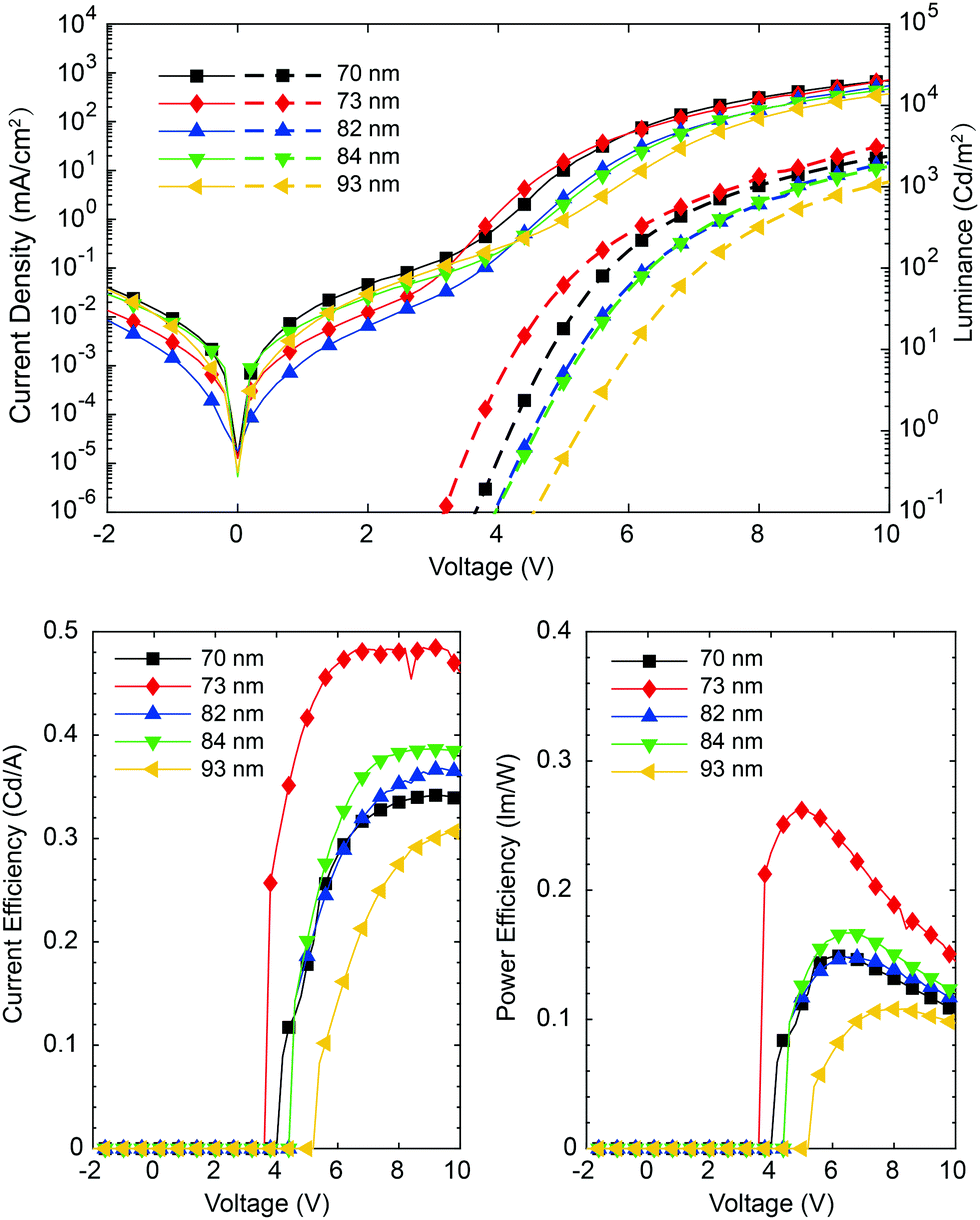 | ||
| Fig. 2 J–V–L, CE and PE curves of F8T2:aza[6]H devices with increasing active layer thickness. | ||
Upon further evaluation of the F8T2:aza[6]H blends, it became apparent that F8T2 allowed for increased aza[6]H loading than F8BT or PFO. Previously, we found that increasing the wt% of aza[6]H > 10% in F8BT:aza[6]H blends resulted in a dramatic decrease of brightness, which renders it challenging to reliably measure gEL.11,13 Given the similar HOMO levels of F8T2 and aza[6]H (∼5.4 eV), a wider range of blend ratios can be studied without aza[6]H acting as a hole trap. We therefore conducted a more extensive inspection of the impact on the relative wt% of the blend components (LEP, aza[6]H) on the chiroptical properties for the first time. The wt% aza[6]H was varied from 10 wt% to 40 wt% (Fig. 4). We note that ratios higher than 40 wt% were not possible due to the formation of crystalline aza[6]H domains, resulting in poor morphology and device operation. As shown in Fig. 4b and Fig. S3 (ESI‡), the electronic transitions of aza[6]H (λ = 350 nm) become visible in the UV-Vis spectra of high wt% blends. For aza[6]H > 20 wt%, polymer emission in the PL spectrum (Fig. S4, ESI‡) is also blue-shifted, which we suggest is caused by disruption of polymer chain packing by excess aza[6]H. This, in turn, reduces the effective conjugation length and results in higher energy emission.21,22 Importantly, the dissymmetry inversion as a function of active layer thickness is no longer observed at the maximum aza[6]H loading (40 wt%): gPL and gEL have the same sign (g ∼ 0.3, Fig. 3). Furthermore, the ellipticity and strength of the Cotton bands of the lowest energy electronic transition decreases as aza[6]H loading is increased (Fig. 4d). To rigorously assess the thickness dependence of CP EL it is essential to combine optical modelling with device engineering (e.g. modifying the electrode reflectivity, tuning the position of the recombination zone), as has been previously demonstrated.13,23,24
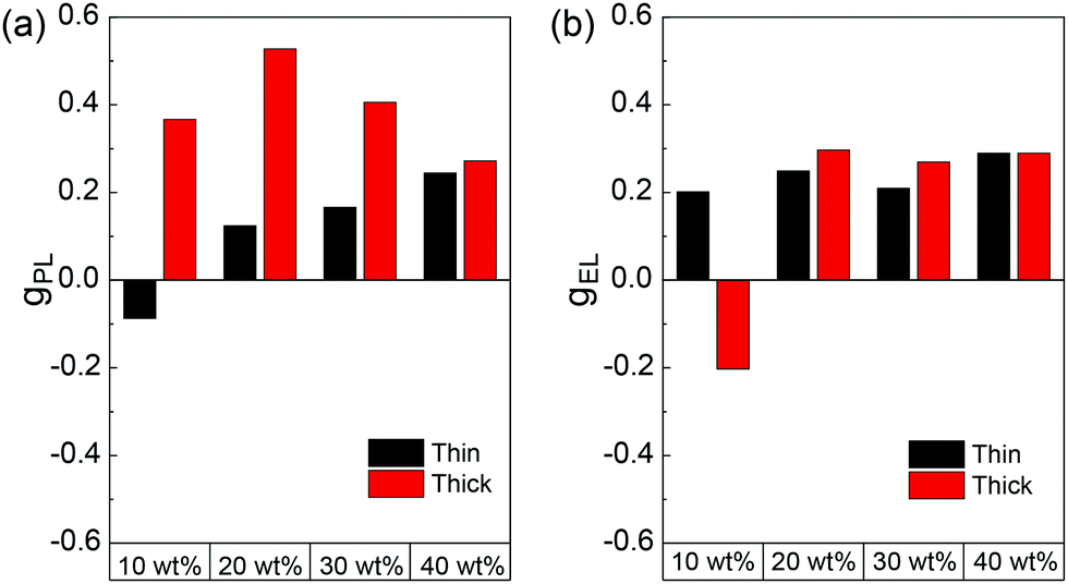 | ||
| Fig. 3 (a) gPL and (b) gEL of thin (∼60 nm) and thick (∼100 nm) F8T2:[P]-aza[6]H films and devices. | ||
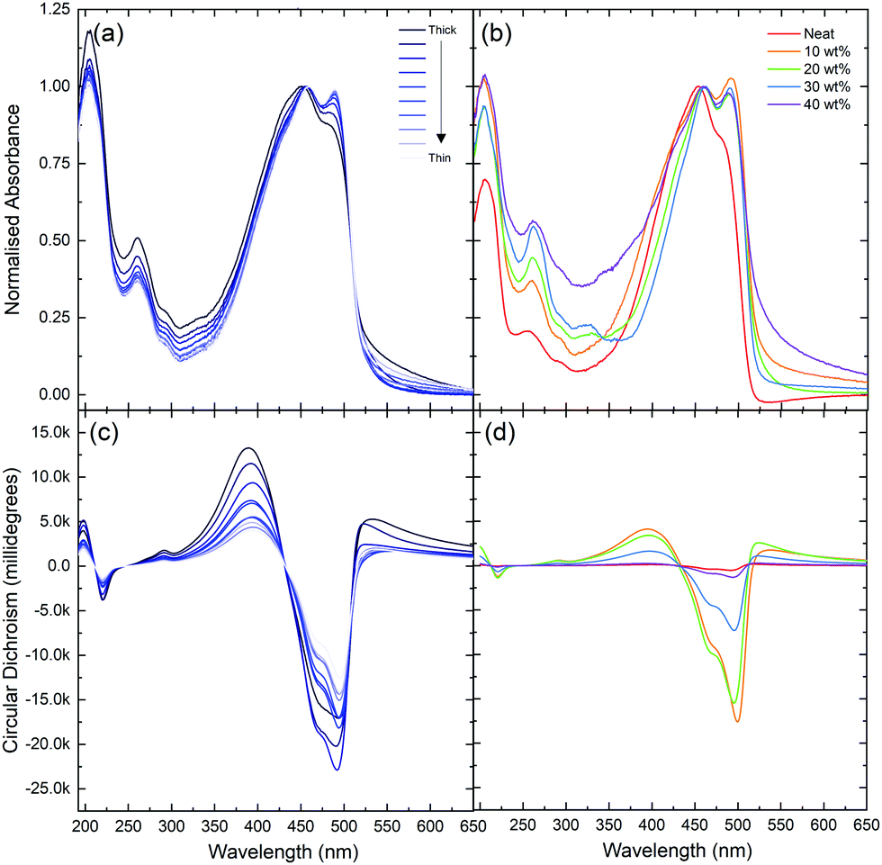 | ||
| Fig. 4 (a and b) Absorption and (c and d) circular dichroism spectra for (a and d) F8T2:10 wt% [M]-aza[6]H blends as a function of film thickness and (b and d) 100 nm thick F8T2: [M]-aza[6]H blends as a function of aza[6]H loading ratio. | ||
The device efficiency of F8T2:[P]-aza[6]H CP OLEDs with thin active layers (60 nm, Fig. 5) increases with aza[6]H wt%. In fact, the 40 wt% aza[6]H device exhibits the best device performance (CE = 0.53 cd A−1, L = 3020 cd m−2 at 10 V) of any aza[6]H blend devices considered here. This impressive device performance indicates that by carefully considering the energy levels of both the achiral polymer and chiral small molecule additive, CP OLEDs with both high gEL and improved device performance can be realized.
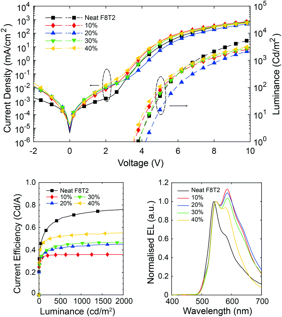 | ||
| Fig. 5 J–V–L, efficiency curves and EL of F8T2:[P]-aza[6]H 60 nm devices with increasing blending ratios of [P]-aza[6]H. | ||
Taken together, this study further confirms that multiple factors influence the sign of the emitted CP light for these materials, independent of the handedness (absolute stereochemistry) of the chiral (polymer) emitter. As described by Duong and co-workers, the coupling of excited states in conjugated LEPs results in degenerate S1 states that give rise to CP PL.18 This implies that in the majority of cases, the sign of CP PL should be consistent with the sign of the CD. However, our previously reported CP-OLEDs,8,9,13 and this work, indicate that film thickness, device architecture and active layer composition also influence the CP emission. The oppositely handed gPL and gEL in F8T2:10 wt% aza[6]H blends also indicate that the mechanisms that underpin the strong CP EL in LEPs are not the same as those that can be used to rationalize the CP PL.
We further show that CP dissymmetry inversion, as a function of active layer thickness, is no longer observed at increased aza[6]H loadings. We attribute this outcome to an increase in the proportion of aza[6]H in the blend, which has a significant effect on polymer structure and packing. Ultimately, it is the structural change of the chiral polymeric phase that determines such chiroptical behaviour,8,10,12 which are impacted by aza[6]H loading. Despite the effect on polymer morphology, very respectable levels of gPL and gEL are still achieved (∼0.3) at high aza[6]H loadings.
Conclusions
Chiral emitters based on LEPs continue to achieve luminescence dissymmetries orders of magnitudes greater than other systems (e.g. g ≈ 1.0). In particular, achiral LEP – chiral small molecule additive blends have presented a simple approach to generate strong CP luminescence of tunable handedness with impressive device performances and many interesting chiroptical phenomena have already been reported. In this study, we have expanded the number of polymers suited to such an approach, through the use of the LEP F8T2. F8T2 blends with low aza[6]H loading further confirm previous observations that highly dissymmetric CP luminescence can be achieved, where the sign of the CP light is thickness dependent and dependent on whether the excitons are optically or electronically generated within the active layer. The same is not true for high wt% aza[6]H blends however, where the overall handedness of the emitted light depends solely on the absolute stereochemistry of the active layer (i.e. F8T2:40 wt% [P]-aza[6]H thin films gEL ∼ +0.3, thick films gEL ∼ +0.3). It is evident that further experimental (for example, evaluating how excited state populations are impacted by drift currents through chiral polymer phases) and theoretical work is required to fully understand and optimize these chiral LEP systems and the CP handedness dependencies and such studies are ongoing in our group.Materials and methods
Materials
1-Aza[6]helicene was prepared as previously reported and separated using preparative chiral HPLC. F8T2 was provided by Sumitomo Chemical Co., Ltd and used without further purification.Solution preparation and thin film deposition
F8T2 was dissolved with a variety of mixing ratios of aza[6]helicene (0, 10 wt%, 20 wt%, 30 wt% and 40 wt%) in toluene (15 mg mL−1). Thin films of various thickness are controlled by spin speed (1200–5000 rpm) and deposited on fused silica substrates. All annealed samples were annealed for 10 min under a nitrogen atmosphere (glovebox, <0.1 ppm H2O, <0.1 ppm O2). The film thicknesses of all films were measured using a Dektak 150 surface profiler.OLED fabrication and characterization
Prepatterned ITO substrates (Thin Film Devices Inc) were rinsed in an ultrasonic bath with acetone, isopropyl alcohol (IPA) and Hellmanex III (Hellma GmbH) and deionized water before deposition of poly(3,4-ethylenedioxythiophene):poly(styrenesulfonate) (PEDOT:PSS) (H.C. Starck GmbH) (55 nm). Then, aza[6]helicene blended F8T2 with varying thickness was spin-coated (1200–5000 rpm) onto PEDOT:PSS. Afterwards, a 25 nm Ca layer capped by a 100 nm Al layer was thermally evaporated onto the organic layer under vacuum level of 1 × 10⁻⁷ mbar. J–V–L characterization (pixel area = 0.045 cm2) was performed using a Keithley 2400 and Konica Minolta LS-110 Luminance Meter via a computer controlled Labview program. EL spectra were measured using an Ocean Optics USB 2000 charge-coupled device spectrophotometer.Photophysical and morphology characterisation
Absorption and PL spectra of the blends at various thickness and blending ratios were measured by a Cary 300 UV-Vis spectrometer (Agilent Technologies) and a FluoroMax-3 (Horiba Jobin Yvon), respectively. Left-handed and right-handed CP PL spectra were acquired using a linear polarizer and quarter-wave plate prior to a FluoroMax-3 spectrometer. The background introduced by the polarizer, the quarter-wave plate and the silica substrates were corrected by using the CP PL results from a blank sample. The dissymmetry factor g in the CP PL spectra was calculated from the equation g = 2(IL − IR)/(IL + IR), |g| ≤ 2. IL and IR are the left-handed and right-handed emission intensities respectively. A similar method was used to analyse the CP EL spectra. EL spectra from the OLED was recorded using an Ocean Optics USB 2000 charge-coupled spectrophotometer.Author contributions
L. W. and J. W. contributed equally to this work.Conflicts of interest
The authors declare the following competing financial interest(s): M. Fuchter is an inventor on a patent concerning chiral blend materials (WO2014016611).Acknowledgements
This work was supported by EPSRC research grants EP/P000525/1, EP/L016702/1 and EP/R00188X/1. We would like to thank the Diamond B23 beamline for assistance with chiroptical measurements.Notes and references
- R. Singh, K. N. Narayanan Unni and A. Solanki and Deepak, Opt. Mater., 2012, 34, 716–723 CrossRef.
- D.-W. W. Zhang, M. Li and C.-F. F. Chen, Chem. Soc. Rev., 2020, 49, 1331–1343 RSC.
- M. Li, Y. Wang, D. Zhang, L. Duan and C. Chen, Angew. Chem., Int. Ed., 2020, 59, 3500–3504 CrossRef CAS PubMed.
- Z. Wu, H. Han, Z. Yan, X. Luo, Y. Wang, Y. Zheng, J. Zuo and Y. Pan, Adv. Mater., 2019, 31, 1900524 CrossRef PubMed.
- X. Shang, L. Wan, L. Wang, F. Gao and H. Li, J. Mater. Chem. C, 2022, 10, 2400–2410 RSC.
- D. Di Nuzzo, C. Kulkarni, B. Zhao, E. Smolinsky, F. Tassinari, S. C. J. Meskers, R. Naaman, E. W. Meijer and R. H. Friend, ACS Nano, 2017, 11, 12713–12722 CrossRef CAS PubMed.
- J. Gilot, R. Abbel, G. Lakhwani, E. W. Meijer, A. P. H. J. H. J. Schenning and S. C. J. J. Meskers, Adv. Mater., 2010, 22, E131–E134 CrossRef CAS PubMed.
- L. Wan, J. Wade, X. Shi, S. Xu, M. J. Fuchter and A. J. Campbell, ACS Appl. Mater. Interfaces, 2020, 12, 39471–39478 CrossRef CAS PubMed.
- L. Wan, X. Shi, J. Wade, A. J. Campbell and M. J. Fuchter, Adv. Opt. Mater., 2021, 9, 2100066 CrossRef CAS.
- J. Wade, J. N. Hilfiker, J. R. Brandt, L. Liirò-Peluso, L. Wan, X. Shi, F. Salerno, S. T. J. J. Ryan, S. Schöche, O. Arteaga, T. Jávorfi, G. Siligardi, C. Wang, D. B. Amabilino, P. H. Beton, A. J. Campbell and M. J. Fuchter, Nat. Commun., 2020, 11, 6137 CrossRef CAS.
- Y. Yang, R. C. Da Costa, D. M. Smilgies, A. J. Campbell and M. J. Fuchter, Adv. Mater., 2013, 25, 2624–2628 CrossRef CAS PubMed.
- B. Laidlaw, J. Eng, J. Wade, X. Shi, F. Salerno, M. J. Fuchter and T. J. Penfold, Chem. Commun., 2021, 57, 9914–9917 RSC.
- L. Wan, J. Wade, F. Salerno, O. Arteaga, B. Laidlaw, X. Wang, T. Penfold, M. J. Fuchter and A. J. Campbell, ACS Nano, 2019, 13, 8099–8105 CrossRef CAS PubMed.
- P. A. Levermore, R. Jin, X. Wang, J. C. de Mello and D. D. C. Bradley, Adv. Funct. Mater., 2009, 19, 950–957 CrossRef CAS.
- J. Veres, S. D. Ogier, S. W. Leeming, D. C. Cupertino and S. M. Khaffaf, Adv. Funct. Mater., 2003, 13, 199–204 CrossRef CAS.
- J. H. Huang, C. Y. Yang, Z. Y. Ho, D. Kekuda, M. C. Wu, F. C. Chien, P. Chen, C. W. Chu and K. C. Ho, Org. Electron., 2009, 10, 27–33 CrossRef CAS.
- Y. Kawagoe, M. Fujiki and Y. Nakano, New J. Chem., 2010, 34, 637 RSC.
- S. T. Duong and M. Fujiki, Polym. Chem., 2017, 8, 4673–4679 RSC.
- R. Jin, P. a Levermore, J. Huang, X. Wang, D. D. C. Bradley and J. C. deMello, Phys. Chem. Chem. Phys., 2009, 11, 3455–3462 RSC.
- M. D. Ward, J. Wade, X. Shi, J. Nelson, A. J. Campbell and M. J. Fuchter, Adv. Opt. Mater., 2021, 2101044 Search PubMed.
- F. C. Spano and C. Silva, Annu. Rev. Phys. Chem., 2014, 65, 477–500 CrossRef CAS PubMed.
- F. C. Spano, Acc. Chem. Res., 2010, 43, 429–439 CrossRef CAS PubMed.
- F. Zinna, M. Pasini, F. Galeotti, C. Botta, L. Di Bari and U. Giovanella, Adv. Funct. Mater., 2017, 27, 1603719 CrossRef.
- D.-M. Lee, J.-W. Song, Y.-J. Lee, C.-J. Yu and J.-H. Kim, Adv. Mater., 2017, 29, 1700907 CrossRef PubMed.
Footnotes |
| † Dedication: To the memory of Professor Alasdair James Campbell. |
| ‡ Electronic supplementary information (ESI) available. See DOI: 10.1039/d1tc05403a |
| § These authors contributed to this work equally. |
| ¶ Present address: Department of Physics, Chemistry and Biology, Linköping University, Linköping 58183, Sweden. |
| || Deceased. |
| This journal is © The Royal Society of Chemistry 2022 |