
 Open Access Article
 This Open Access Article is licensed under a Creative Commons Attribution-Non Commercial 3.0 Unported Licence
Interconnected three-dimensional anodized aluminum oxide (3D-AAO) metamaterials using different waveforms and metal layers for RGB display technology applications†
Cristina V.
Manzano
 ,
Julia
Rodríguez-Acevedo
,
Olga
Caballero-Calero
and
Marisol
Martín-González
*
,
Julia
Rodríguez-Acevedo
,
Olga
Caballero-Calero
and
Marisol
Martín-González
*
Instituto de Micro y Nanotecnología, IMN-CNM, CSIC (CEI UAM + CSIC) Isaac Newton, 8, E-28760, Tres Cantos, Madrid, Spain. E-mail: cristina.vicente@csic.es; marisol.martin@csic.es
First published on 5th January 2022
Abstract
Research into the artificial reproduction of vibrant colours in natural creatures and the reproduction of their structural colours has generated considerable interest. One inorganic material that has been studied for the generation of these artificial colours is anodic aluminium oxide (AAO). For example, 3D anodic aluminium oxide (3D-AAO) metamaterials act as distributed Bragg reflectors. This study examines the effect of the application of various waves (square, sinusoidal, and sawtooth) during the generation of 3D-AAO on the optical and morphological properties of these 3D metamaterials. The effect of the waveform in the colours and hues has been explained by a theoretical model. Furthermore, the work analyses how colour can be improved by depositing a thin metal layer on top, obtaining, from a simplistic point of view, a combination of two effects: a Bragg reflector (3D-AAO) and an optical reflector (metal mirror). For that, different metals like Au, Pt, and Cr have been studied. The thickness of the metal layer has been theoretically modelled. This study paves the way for a new approach to developing structural colours for their use in for example RGB display technologies.
1. Introduction
The bright colours of the creatures of nature have aroused considerable interest.1 Many living creatures exhibit photonic behaviour in different parts due to their internal micro/nanoscale structure. In recent years, the study of materials capable of reproducing the same photonic effects of these natural systems has increased due to the wide range of possible fields of application. One of these fields is electronic display technology, where perfect control over colour generation is essential, and for this reason, plasmonic structural colours have received great attention.2 There are different techniques to fabricate these plasmonic structural colours, such as electron beam3 or laser lithography,4 focused ion beam,5 colloidal self-assembly,6 inkjet printing,7 anodization,8etc. Anodization of aluminum, makes it possible to obtain anodic aluminium oxide nanostructures.The fabrication of photonic crystals using anodic aluminium oxide (AAO) was first published in 1999 by Masuda et al.9 and the first study where a changed colour was observed was reported in 2007.10 In this last study, a combination of linear and sinusoidal waves was applied to obtain a modulation in the pore diameter along with the longitudinal pores of the alumina. One year later, Gösele's group11 published for the first time pulsed anodization between mild and hard anodization regimes to obtain different modulation in the pore diameter along the alumina thickness. Modulated Au and Ni nanowires inside these types of templates were electrodeposited by Sulka et al.12 in 2011. In the same year, Yisen et al.13 reported the application of these nanostructures anodized by pulsed anodization between mild and hard anodization as photonic crystals; and one year later, Sulka et al.14 published the use of these nanotemplates as Bragg reflectors. Several studies were reported by Santos et al.15–17 on the morphological and optical properties of modulated AAO but not in interconnected 3D nanochannels. In 2014, our group reported for the first time a new method based on pulsed anodization followed by a chemical etching to obtain interconnected three-dimensional nanochannels inside anodic aluminium oxide (3D-AAO) nanostructures.18 The study of the optical properties of these 3D-AAO templates was analysed in detail,19,37 showing a Bragg reflector behaviour. Additionally, the fabrication of metamaterials of different materials and properties (semiconductors, magnetic, and polymeric materials) have been produced inside these 3D-AAO templates and the novel properties of these metamaterials are studied.20–23,38–40 In all these studies, the 3D-AAO were produced by a square wave combining hard and mild conditions during anodization with an ulterior chemical etching to obtain the interconnected nanopores. In 2019, a study with sinusoidal and sawtooth waveforms applied during anodization to modulate the alumina was performed. The optical properties of the obtained AAO nanostructures were also reported. The applied pulses in that work were between a positive voltage and their reversed voltage, to accelerate the corrosion of the alumina,24 which is different to the approximation used in this work. Moreover, the different waveforms have not yet been applied to the fabrication of 3D-AAO templates. In addition, their influence on the structural colours has not been performed. The anodization is a cost-effective and scalable to industry method, due to the possibility to fabricate them in large areas. This approach seems ideal for electronic display technology. For this reason, a study focusing on the influence of different waves during the pulsed anodization is indispensable for the development of not only RGB devices but also new metamaterials based on these nanostructures.
Finally, to increase the degrees of freedom (layer's material and thickness) that can be modified to generate a larger palette of colors in the 3D-AAO, a thin metal layer was deposited on the 3D-AAO. It is well-known in more conventional porous aluminas that their colours can be tuned by adding a metal layer on top.8,25–29 But the effect of those metal coatings on 3D-AAO nanostructures has never been studied.
In this work, the 3D-AAO metamaterials are produced by applying three different waves (square, sinusoidal or sinusoid, and sawtooth) during pulsed anodization. This makes possible to control both the length between the consecutive transversal pores of 3D-AAO (because of the period used between the pulses) and the shape, width, and height (aspect ratio) of the transversal pores (due to the type of wave used). This approach is a new way to tune the shape and aspect ratio of these Bragg reflectors. The effect of the different applied waves (square, sinusoidal, and sawtooth) on the optical and morphological properties of the nanostructures was analysed from both the experimental and the theoretical points of view. Additionally, a thin metal layer was deposited on the three different 3D-AAO nanostructures to activate the structural colour found in these anodized films three different metals (Au, Cr, and Pt) were used, obtaining a combination of two effects, Bragg reflector (3D-AAO nanostructures) and an optical reflector (metal mirror).
2. Results and discussion
2.1. Anodization curves of 3D-AAO Bragg reflectors using different applied waves
To change the photonic behaviour of the Bragg reflectors based on ordered three-dimensional anodic aluminium oxide (3D-AAO) nanostructures, three different wave-shapes were used in the second anodization step: square, sinusoidal, and sawtooth. The thickness of the nanostructures depends on the total number of pulses. In this study, the number of pulses was set at 150 to ensure manipulation and a total thickness of 35 μm was achieved.As it is explained in the Experimental section, a chemical etching is carried out after the second anodization, which consists of pulsed anodization between soft and hard anodization. It is during this chemical etching where the transversal channels of the nanostructures are opened, given that the alumina anodized during the hard anodization has a faster etching rate than the alumina made during the mild anodization. By controlling the chemical etching time, it is possible to open the transverse interconnecting channels. At the end of the process, the longitudinal and transversal channels are interconnected, forming the three-dimensional anodic aluminium oxide (3D-AAO) nanostructures. Table 1 shows the anodization conditions and etching time used for the different three-dimensional AAO nanostructures. Each of these nanostructures was fabricated with each applied wave (square, sinusoidal, and sawtooth). This table also collects the etching time for the different rest times (180, 240, 300, and 360 s).
| V r (V) | t r (s) | V p (V) | t p (s) | Total anodization time (s) | Etching time for square (s) | Etching time for sinusoidal (s) | Etching time for sawtooth (s) |
|---|---|---|---|---|---|---|---|
| 25 | 180 | 33 | 2 | 28![[thin space (1/6-em)]](https://www.rsc.org/images/entities/char_2009.gif) 800 800 |
1398 | 1424 | 1413 |
| 25 | 240 | 33 | 2 | 37920 |
1261 | 1740 | 1756 |
| 25 | 300 | 33 | 2 | 46800 |
1581 | 1749 | 1618 |
| 25 | 360 | 33 | 2 | 55920 |
2110 | 2221 | 2281 |
The optimum etching time to open the transverse pores differed depending on the wave used in the anodization and the total thickness of the template. It can be concluded that when the overall thickness is increased the total etching time is also increased. So, the opening of the transverse pores needs to be optimized for each type of template. Moreover, the etching time for the square wave is lower than that of sinusoidal or sawtooth.
Fig. 1 shows the current density as a function of time for the different waveforms when the rest time is 180 s. In this figure, the recuperation time (time required for the current density to go back to a mild anodization steady value) are compared. It is interesting to note that when a square wave is applied, the longest recuperation time is required, in comparison to the sinusoidal, and sawtooth waves, which are similar. This can be explained by the fact that in the square wave the alumina remains the longest under hard anodization conditions. Whereas the sawtooth is the shortest. This behaviour was observed no matter the resting time used (240, 300, and 360 s) to obtain the different Bragg reflectors.
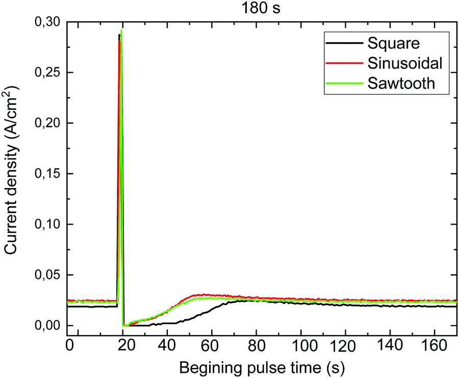 | ||
| Fig. 1 Current density versus time for the different waves (square, sinusoidal, and sawtooth) for a rest time of 180 s. | ||
2.2. Effect of applied waves on the optical properties and morphology of 3D-AAO Bragg reflectors
The reflectance spectra based on the wavelength of the different 3D-AAO can be found in Fig. 2A–D. The inset in Fig. 2A–D shows the optical images of these nanostructures obtained with different waves and rest periods. From the reflectance spectra, it can be concluded that when the rest time is higher the maximum reflected wavelength is shifted to red, as it can be observed by the optical images, the hue is different depending on the type of wave used (see inset of Fig. 2A–D).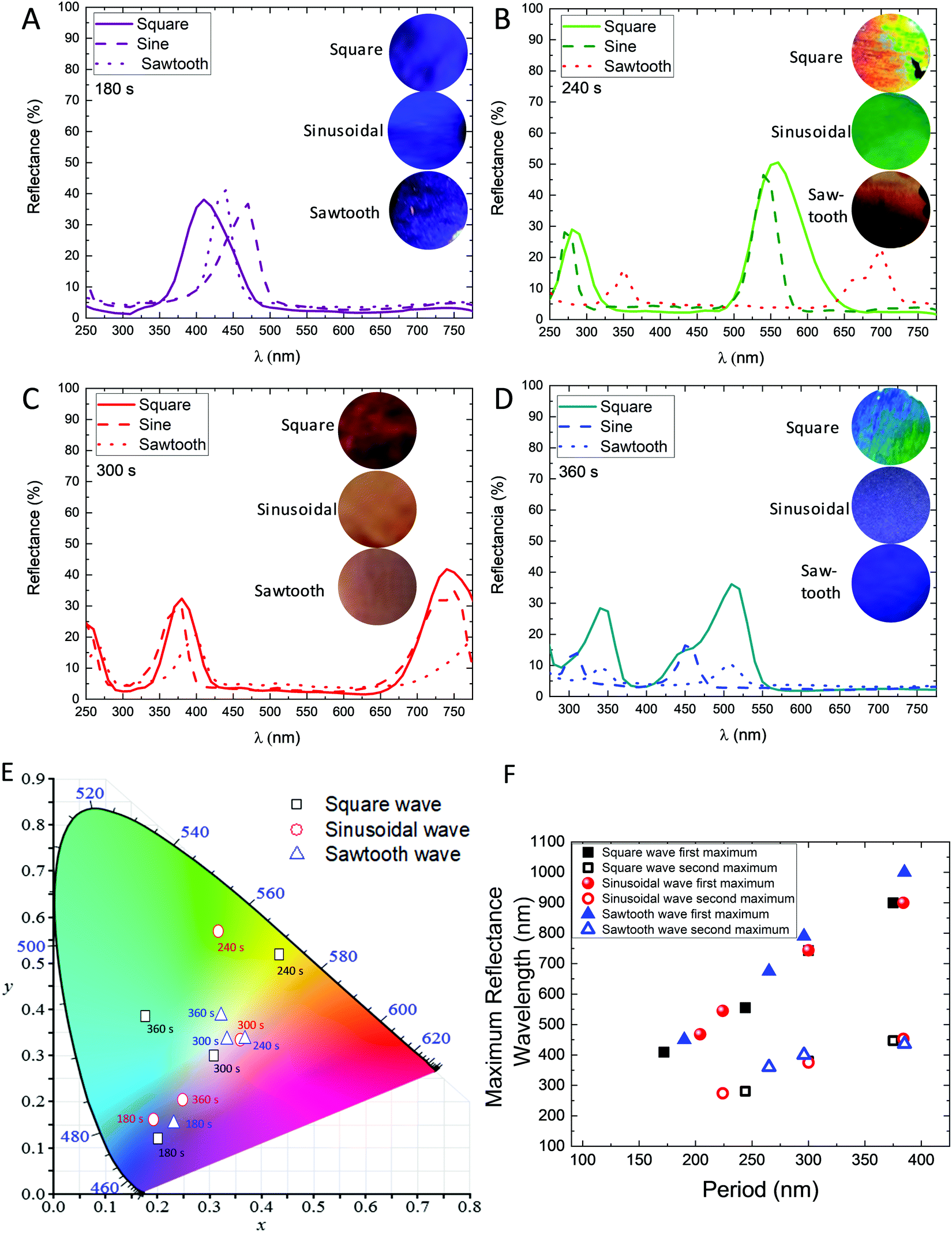 | ||
| Fig. 2 UV-Vis reflectance spectra as a function of the wavelength of 3D-AAO nanostructures or different waves and rest times. (A) 180 s, (B) 240 s, (C) 300 s, and (D) 360 s. In the inset, optical images of 3D-AAO colour for different waves and resting times were studied. (E) Colour diagram (chromaticity, xy) of 3D-AAO nanostructures for different waveforms and rest times between pulses in seconds, and (F) maximum wavelength of the experimental reflectance spectra as a function of the period (sum of the distance of two adjacent pores plus the length of the pores). Closed symbols represent the first maximum obtained, and open symbols, the second maximum. In both graphs, black represents the 3D-AAO generated by a square wave, red show those generated using a sinusoidal wave, and blue are those fabricated by the sawtooth wave. | ||
The different rest periods result in similar transversal pore distances, regardless of the applied wave (see Fig. 2E and F). The small variations are due to the difference in the etching time between them. As expected, when the maximum of the wavelength obtained in the reflectance spectra is plotted as a function of the period of the 3D structure, an almost linear behaviour is observed (see Fig. 2F), given that this parameter defines the Bragg structure created. The xy (chromaticity) was calculated from the reflectance as a function of wavelength for each nanostructure. Fig. 2E shows the colour diagram (xy) of the different nanostructures obtained in this study. In the inset of the figure, it can be observed the values of the period between the transversal channels of each nanostructure. As it can be observed in Fig. 2E, the colours and hues are different for nanostructures anodized under different waveforms, even when the period between two transversal channels is the same. It can be concluded that, while the colour in these Bragg reflectors can be nanoengineered depending on the period between transversal channels, the hues can be tuned by the different waves applied. Therefore, the type of wave used can introduce an extra parameter to modify the internal structure of these 3D-AAO templates covering the whole colour gamut. This variation is due to the morphological structure of the alumina, given that the porosity of the transversal channels is different depending on the applied wave, as is shown in FE-SEM images of Fig. 3.
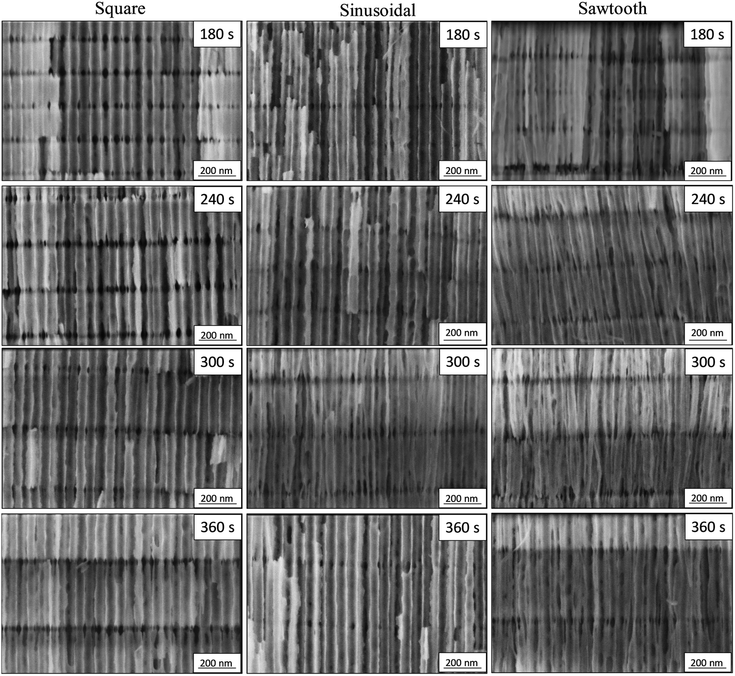 | ||
| Fig. 3 FE-SEM images of all the fabricated 3D-AAOs: left square wave, centre sinusoidal wave, right sawtooth wave. The different rest times are (from top to bottom), 180 s, 240 s, 300 s, and 360 s. | ||
From the FE-SEM images, the width and length of the transversal pores of the 3D-AAO were calculated, to know the effect of the applied wave on the morphology of the transversal pores. These values were measured in three different parts of each nanostructure (close to the top, bottom, and middle parts), where six measurements were taken in each of these parts. The values given in Table 2 represent the average over different measurements taken from different SEM images. The pore diameter of the longitudinal channels was measured on the top view of FE-SEM images of the nanostructures, and an average of several measurements gave pore diameters of 55, 54, and 53 nm for square, sinusoidal, and sawtooth waves, respectively; the pore diameter of the longitudinal pores is the same independently on the applied wave.
| Wave | Resting time (s) | TP width (nm) | TP height (nm) | TP inter-distance (nm) | Total 3D-AAO thickness (μm) |
|---|---|---|---|---|---|
| Square | 180 | 29 | 52 | 120 | 29 ± 3 |
| Square | 240 | 32 | 56 | 188 | 39 ± 4 |
| Square | 300 | 26 | 59 | 241 | 47 ± 5 |
| Square | 360 | 26 | 55 | 320 | 61 ± 6 |
| Sinusoidal | 180 | 22 | 45 | 159 | 32 ± 3 |
| Sinusoidal | 240 | 25 | 35 | 189 | 37 ± 4 |
| Sinusoidal | 300 | 23 | 48 | 252 | 48 ± 5 |
| Sinusoidal | 360 | 22 | 49 | 335 | 52 ± 5 |
| Sawtooth | 180 | 16 | 74 | 116 | 30 ± 3 |
| Sawtooth | 240 | 20 | 78 | 187 | 45 ± 5 |
| Sawtooth | 300 | 15 | 74 | 222 | 48 ± 5 |
| Sawtooth | 360 | 23 | 84 | 301 | 59 ± 6 |
Based on morphological characterization, it can be concluded that when a square wave is applied, the transverse pores are wider than when a sinusoidal wave is used. In the case of the sawtooth wave, the pores obtained are narrower than in the previous cases. The width of the pores is larger when a square wave is applied than when sinusoidal or sawtooth waves are used being the narrowest the sawtooth wave. The largest height of the transversal pores is found for the sawtooth wave, while the smallest height is observed for the sinusoidal wave. For the three studied cases, the pores have an oval shape; being the pores which present the most oval shape those obtained using a sawtooth wave (the largest difference between the dimensions of the width and height) and the lowest oval shape the anodized using the sinusoidal wave (the smallest difference between the dimensions of the width and height). In conclusion, the shape of the transverse pores can be controlled by the applied wave, or in other words, the ovality of the interconnected nanochannels depends on the total time the system is in hard anodization conditions. The distance between two pores, measured from the bottom part of one of the pores to the top part of the other pore, is larger when the rest time is longer, as expected. This distance is similar independently on the applied wave for the same rest time. The shape of the wave applied modified the morphological properties of the transversal channels of the 3D-AAO nanostructures and, then, the porosity of these channels. The observed change in the porosity leads to a different refractive index in the transversal channels.19 This makes that the optical behaviour of the 3D-AAO nanostructures is different for each wave.
In addition, the thickness of the nanostructures was measured from FE-SEM images (see Table 2). The thickness was similar for the different waves; however, this magnitude depends strongly on the rest time, as it was reported before.19 The thickness was found to be approximately 30, 40, 50, and 60 μm for rest times of 180, 240, 300, and 360 s, respectively. It is important to note that the three-dimensional nanostructures anodized using square and sinusoidal waveforms exhibit better mechanical stability than the nanostructures obtained using sawtooth waves.
To reproduce the experiments, a model to represent these Bragg reflector structures was applied based, on the theoretical model of ref. 19, which should lead to the corresponding reflectance spectra obtained experimentally. Therefore, the model was formed by superlattices of alternating layers of (1) the longitudinal nanoporous layer –n1– with (2) a layer where transversal nanochannels –n2– are present (see Fig. 4A–E). For the model, the experimental geometrical parameters obtained by SEM were used. For 3D-AAO obtained by square waveform, the theoretical reflectance obtained matched the experimental one for all the rest times used (see Fig. 4D and E). For that, a slight modification in the refractive index value of the alumina versus the one in the database of the program used for the simulations was required. That was because the porous alumina is amorphous and has a lower value.8 The match between the experiment and theoretical results corroborates that the square wave model can be explained using two different refractive indexes (n1 and n2), observing two different porosities in the 3D-AAO nanostructures. Then, 3D-AAO nanostructures anodized using a square wave can be modelled using superlattices of alternating layers model of two different refractive indexes due to the change of the porosity observed in the nanostructures between the transversal and longitudinal channels caused by the application of mild and hard anodization, respectively.
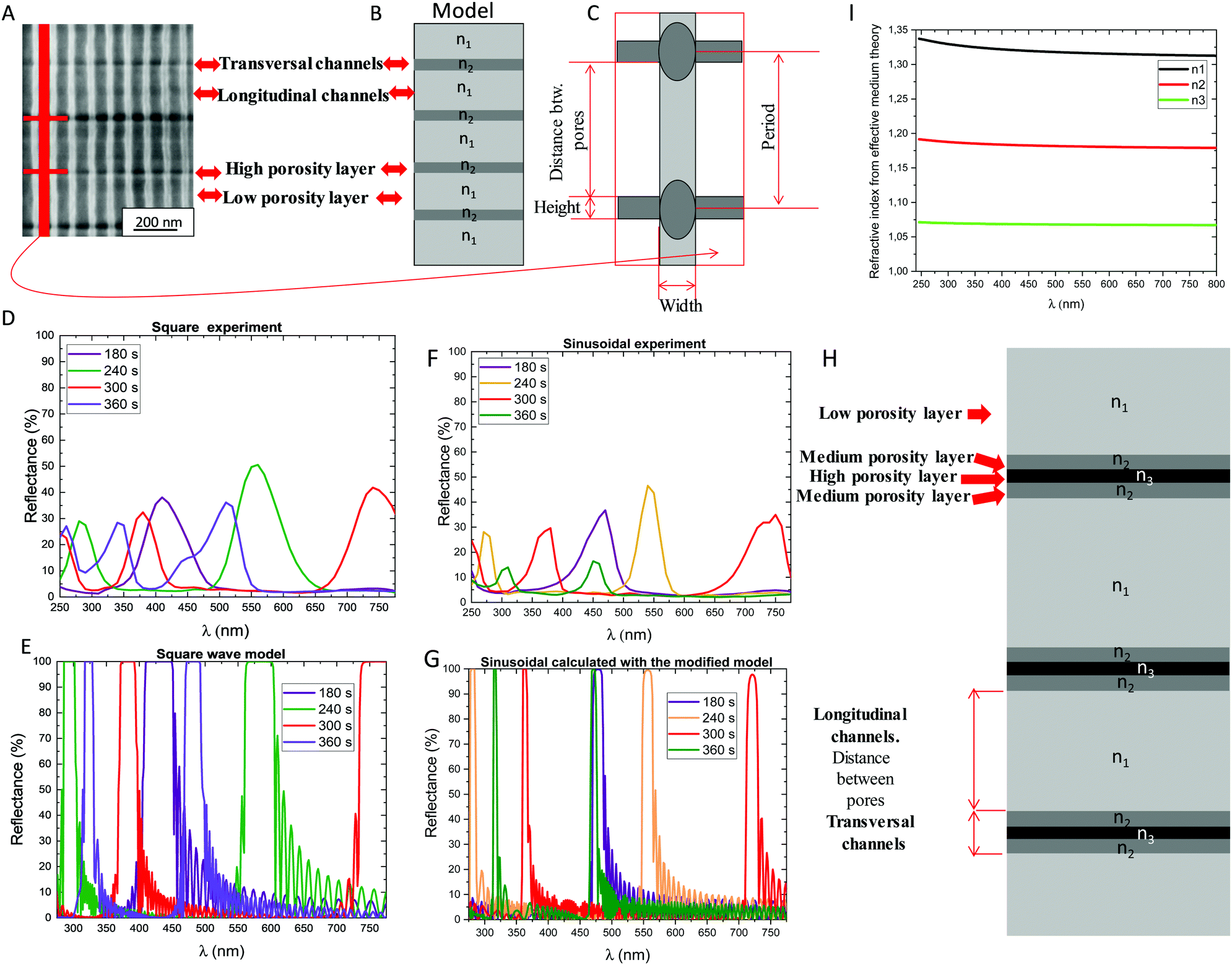 | ||
| Fig. 4 (A) Detail of SEM image of a cross-sectional view of a free-standing 3D-AAO and the schematic view of the channel structure, (B) interpretation of the schematic view into the model, where the longitudinal channels are substituted by a low porosity layer with a thickness which corresponds to the “distance between adjacent pores” measured experimentally, and the regions of the connecting transversal channels are substituted by a higher porosity layer with a thickness corresponding to the length of the nanopores measured, and (C) shows an inset in the schematic view showing the correspondence between the period of the periodic structure, the length of the nanopores and the distance between two adjacent nanopores, (D) experimental reflectance spectra collected for the different 3D-AAOs fabricated with square waves and different rest pulses, and (E) the theoretical reflectance spectra obtained with the theoretical model of layers depicted for the square wave. Comparison between the (F) experimentally obtained spectra for the different rest times in the case of the sinusoidal wave and (G) the theoretically obtained maxima when the model is modified to consider the different morphology of the transversal channels. This was made by substituting the layer that represents the transversal channels by three layers of different porosities, as schematically depicted in figure. (H). (I) Refractive index from effective medium theory as a function of the wavelength. As it can be seen, theory and experiment are in good agreement. | ||
In the case of the 3D-AAO metamaterials fabricated with the other waves (sinusoidal and sawtooth), the model of the alternating layers with the geometrical parameters extracted from the morphological characterization did not reproduce the obtained experimental spectra (see Fig. S1A–D of the ESI†). As a result, it had to be modified to consider somehow the different morphologies of the transverse pores measured by FE-SEM. This was done by maintaining the properties of the layers that correspond to the longitudinal pores in the structures (that is, the effective index of those layers and the distances measured by SEM) but modifying the properties of the layers corresponding to the parts of the transversal channels, to consider their different morphologies. These affect the porosity of those layers and, therefore, the effective index obtained by the effective medium theory.
In the case of the sinusoidal wave, the layer representing the transversal channels was modelled using three different layers. Therefore, three different refractive indexes are considered in this model (n1, n2 and n3), to represent three different porosities in the 3D-AAO sinusoidal wave fabricated nanostructures. The index corresponding to the longitudinal layer, n1, is the same as in the case of the square wave. Nevertheless, to consider that the porosity in the transversal channels in the sinusoidal wave is not homogeneous, two additional layers were implemented. The experimental results could be simulated theoretically (see Fig. 4F–H) using a superlattice of alternating layers, but in this case, introducing three different refractive indexes due to the three different porosities observed.
In the case of the sawtooth, the mismatch between the square wave model and the experiment was the largest (see Fig. S1B and D, ESI†), and due to the complex morphology, that it presents, it was not straightforward to reproduce the results with a simple superlattice model, by only changing the properties of the layers associated to the transversal channels. For the sawtooth wave, the width of the transversal channels’ changes depending on the applied rest time, for this reason, it is not possible to perform a model which can simulate the experiments. This change in the width modifies the porosity, and consequently, the refractive index for each rest time.
Then, it is evident that the changes in the optical response for each of the nanostructures (hues) produced with different waves should be related to both the morphology of the transversal pores and the final porosity of the transversal layer, as the model corroborates for the cases of square and sinusoidal waves.
In order to use these nanostructures as emerging display technologies2 such as RGB devices, the activation of the colours observed in 3D-AAO nanostructures is fundamental. The observed colours can be enhanced by the deposition of a metal layer on the 3D-AAO Bragg reflectors. To achieve this, a metallic layer of 100 nm of Au, Cr, and Pt was deposited on the surface of the structure. The 3D-AAO colour changes can be observed in Fig. 5, obtaining a combination of two effects, the effect of a Bragg reflector (3D-AAO nanostructures) and the effect of an optical reflector (metal mirror). These experiments were only performed in the nanostructures anodized using square and sinusoidal waves due to the low mechanical stability of the 3D-AAO nanostructures anodized using the sawtooth wave.
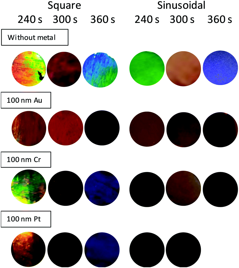 | ||
| Fig. 5 Optical images of the 3D-AAO nanostructures after 100 nm Au, Cr, and Pt metal deposition. | ||
The hue before and after the metallization is slightly different, and that hue depends on the metal deposited. From the simulated reflectance spectra (Fig. 6B and C), it is shown that the main different appears between Au and the other two metals (Cr and Pt), that explains the slight difference in the hue. To understand the behaviour of the reflectance in the 3D-AAO upon the different metals evaporated, the simplistic simulation explained above of the alternating layers for the structures formed with the square wave was modified to include 100 nm of the different metals.
Fig. 6A presents the results from two different rest times for the square wave templates. The deposit of platinum and chromium have a higher and flatter reflectance over the entire visible range. The observed colour is due to two contributions, the colour of the 3D nanostructure and the colour of the metal. Depending on the deposited metal, the colour of the 3D nanostructure can be modified. This behaviour is completely different to the behaviour observed when a metal layer is deposited on the 1D-AAO nanostructure, where the final colour is only due to the metal deposited because the original nanostructures are transparent.
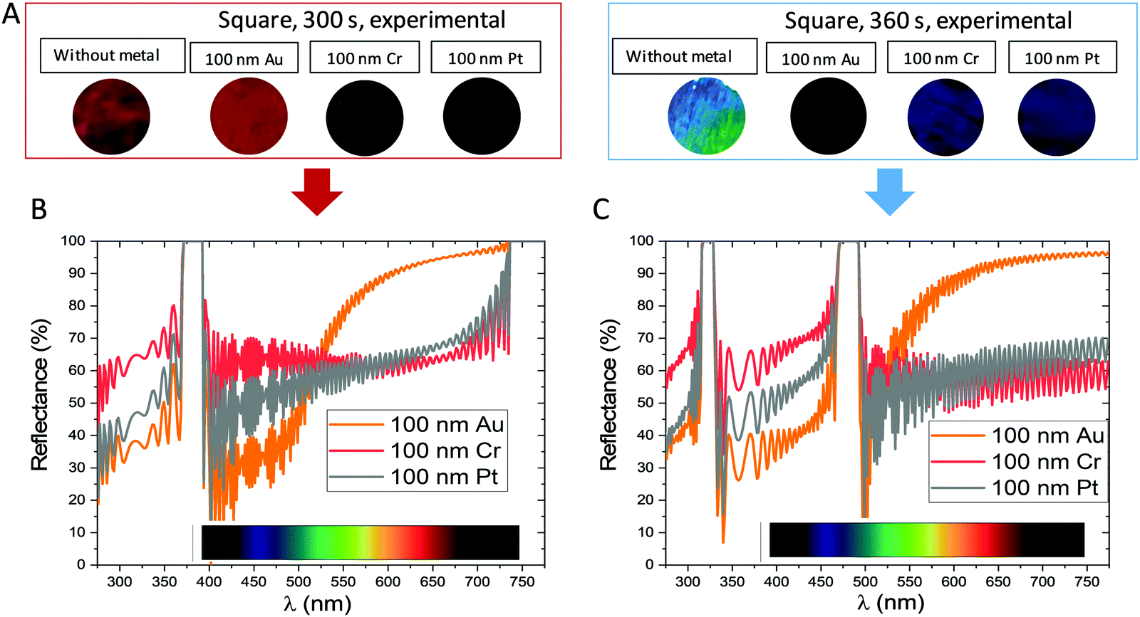 | ||
| Fig. 6 (A) Detail of the photo of the different colours that the different 3D-AAO fabricated with square wave present after the deposit of Au, Cr, and Pt, (B and C) simulated reflectance spectra of the 3D-AAOs with the different deposited metals (orange Au, red Cr, and grey Pt) for 300 s and 360 s rest time, respectively. The colour scale has been included in (B and C) as an extra guide for the resulting colours explained in the text. | ||
In the case of 300 s rest time, the 3D-AAO nanostructures with Pt or Cr deposited show no particular colour, and this can be understood when seeing the simulated spectra, given that they have maxima in the infrared and ultraviolet range. In the case of the gold deposit, it presents an orange-red colour, which corresponds to the simulated reflectance, where the gold presents a higher reflectance in the orange-red part of the spectrum. In the case of 360 s rest time, the three metals produce a blueish colouration of the structure, being much more metallic and well defined for chromium and platinum than for gold. Again, when the simulated spectra are considered, it is easy to see that both Pt and Cr again show a high reflectance throughout all the visible spectra, but this time with a maximum corresponding to blue, which gives the structures this metallic blue colouration. In the case of gold deposit, this blue colour is less strong, given that apart from the maxima in the blue region, the simulated spectrum also presents another of high reflectance around the same region as before, and thus, the colour is less defined, and the metallic shine is less evident than with the other two metallic layers. Then, the modified model for simulating the nanostructures (Fig. 6B and 7C), can also predict the effect of metallic layers and how they will modify and enhance the structural colouration of the 3D-AAO nanostructures.
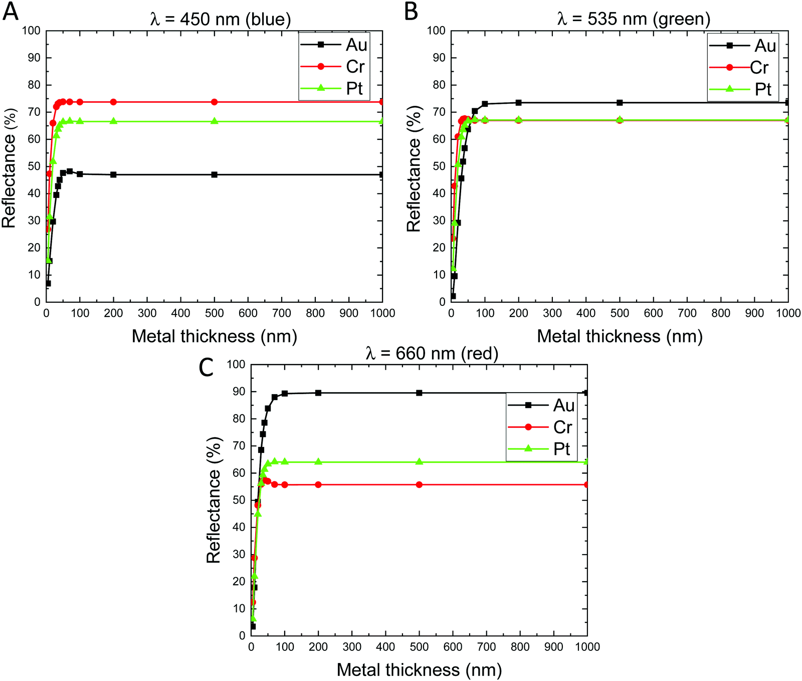 | ||
| Fig. 7 Simulated reflectance as a function of the metal thickness for the 3D-AAO/metal nanostructures generated by a square wave for different wavelengths: (A) 450 (blue), (B) 535 (green), and (C) 660 (red). | ||
Once that the model works for the 3D-AAO nanostructures anodized applying the square and sinusoidal waves with different metals evaporated, the metal thickness (from 5 to 1000 nm) for the case of Au, Cr, and Pt was analysed for a 3D-AAO Bragg reflector anodized using a square wave with a period of 360 s using the previous model (see Fig. S2, ESI†).
Fig. 7 shows the simulated reflectance as a function of the metal thickness for the 3D-AAO/metal nanostructures for three different wavelengths: 450, 535, and 660 nm. This figure was obtained using the simulated data of Fig. S2 (ESI†). As it is shown in Fig. 7, for metal thicknesses in the range of 5 to 70 nm there is an enhancement in the colour upon increasing the metal thickness. But, for thicknesses upon 100 nm, the observed colour becomes practically identical, so no big improvements are obtained by layers thicker than 100 nm. This behaviour is observed independently of the metal deposited on top (Au, Cr or Pt) and of the wavelength studied (450, 535, and 660).
In the case of 450 nm, the highest reflectance (∼0.75) observed is for Cr; while the smallest is observed for Au (∼0.45). So, the blue colour (which roughly corresponds to the range of 450–495 nm) is enhanced by adding Cr metal. For 535 nm the highest reflectance (∼0.75) is obtained for Au, and the reflectance is similar for Cr and Pt (∼0.65). So, it can be concluded that the green colour (which is in the range from 495 to 570 nm) is improved by the deposition of an Au layer on 3D-AAO templates. In the case of 660 nm, the highest reflectance (∼0.9) observed is for Au; while the smallest is observed for Cr (∼0.55). Then, the red colour (which is in the range 620–770 nm) is enhanced by the addition of an Au metal film on top. In conclusion, depending on the desired colour for the RGB device, the metal deposited on the 3D-AAO nanostructure can be Au for the enhancement of red and green, and Cr for blue. While Pt does not seem to be a good option for the color range studied.
3. Conclusions
3D-AAO metamaterials have been fabricated using different waveforms (square, sinusoidal, and sawtooth) during pulse anodization. For the three waveforms, the transversal pores have an oval shape. The ovality is controlled by the type of waveform used. The largest width of oval transversal pores was obtained when a square wave was applied and the smallest one was observed for the sawtooth wave. The largest height of the transversal pores was obtained when the nanostructures were anodized using the sawtooth, while the smallest height observed was for the case of the sinusoidal wave. The distance between two transversal adjacent pores depends on the resting time, but it is similar independently on the applied wave. The thickness of the 3D-AAO nanostructures depends on the rest period, but it does not depend on the applied wave. 3D-AAO anodized using square and sinusoidal waves offer better mechanical stability than the nanostructures obtained with a sawtooth wave.It can be also concluded by studying their optical properties that the colour found in these nanostructures depends on the period between transversal channels, while the colour and the hue of these nanostructures depends on the waveform, which is related to the internal morphology (porosity) of the transversal pores. To understand it a theoretical model was used. A two layers model with two different refractive indexes are used for square wave fabricated 3D-AAOs. While for sinusoidal waves the model used to fit their optical response, is more complex. This explains why the hue observed is different for the same resting times, but different wave shapes. The nanostructures with a rest time of 360 s present also a response in the near-infrared region, while the rest of the nanostructures have a certain response only in the UV-Vis region.
Furthermore, we have shown that an additional way of tuning the colour of 3D-AAO nanostructures is by depositing a thin metal layer, obtaining the combination of two effects, the effect of a Bragg reflector (3D-AAO nanostructures) and the effect of an optical reflector (metal mirror). We have deposited Au, Cr, or Pt. Different hues are observed before and after the metallization, which has been studied by a theoretical model. Thus, changes and properties of future experiments can be predicted, and the structural colouration enhanced and tuned. The thickness of the metal layer has been concluded to be 70 nm. Depending on the desired colour, the metal deposited on the 3D-AAO nanostructure must be different. For blue, Cr is the best choice, while for green or red colours, Au is the best option. The combination of the 3D-AAO nanostructures and a thin metal film deposited on the nanostructures opens a new path for nanoengineering this structure for RGB display technology applications.
4. Experimental methods
4.1. Fabrication of 3D-AAO Bragg reflectors using different applied waves and metals deposition
Three-dimensional self-ordered anodic aluminium oxide films were fabricated using a two-step anodization process30 under conditions similar to those used in previous manuscripts.18,19 The electrolyte, temperature, and voltage applied were 0.3 M H2SO4, 0 °C, and 25 V, respectively. The first anodization step consists of applying a constant potential for a certain time to obtain the ordering of the pores.31–34 After removing the alumina formed in this first step, the second anodization consists of pulsed anodization between mild (during specific rest time) and hard anodization (during a pulse time) conditions, between two different potentials (25 V and 33 V, respectively). Once the process of anodization was complete, the aluminium substrate was removed using a CuCl2 and HCl aqueous solution, and the barrier layer was opened using 10 wt% H3PO4 for 10 min at 30 °C. Consequently, a 3D-AAO membrane was obtained, after chemical etching using 5 wt% H3PO4 at 35 °C was performed to open the transversal pores, as it was done in previous works for 3D-AAO structures.18,19In this work, three different waves have been applied in the second step: square, sinusoidal, and sawtooth waves. The pulse time (tp) was maintained for 2 s (up to 33 V). For each type of wave, the rest time (tr) was varied between 180, 240, 300, and 360 s (at 25 V) to change the distance between traversal channels. The maximum current density was limited to 0.3 A cm−2 to prevent damage in the anodic aluminium oxide structures, as it was explained in previous studies.18 A scheme of these different waves, along with the important parameters involved, are shown in Fig. 8.
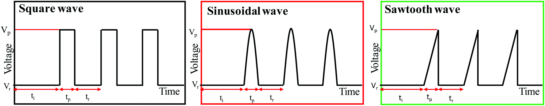 | ||
| Fig. 8 Diagram of the different waves applied during the pulsed anodization. Where Vp is pulsed voltage, Vp is pulsed voltage, Vr is rest voltage, ti is the initial time, tp is pulsed time, and tr is rest time. | ||
To carry out the experiments it was necessary the development of a LabVIEW® program to control the actual voltage provided by the power sources during the experiment and control the different parameters of the pulsed anodization (rest times, number of pulses, type of pulse, etc.). The MATLAB® Script tool of LabVIEW® was used to generate the different waves required by defining the function, then feeding them to the LabVIEW® control program.
Finally, the 100 nm gold, chromium, and platinum layers were deposited by electron beam. These metals were chosen due to their significant ability to improve interference and colour tuning capabilities.28 The metal deposition times were 1100, 934, and 1100 s for Au, Cr, and Pt, respectively.
4.2. Characterization of 3D-AAO Bragg reflectors using different applied waves
Morphological characterization was conducted using high-resolution field emission scanning electron microscopy (FE-SEM, FEI VERIOS 460) with a 2 kV accelerating voltage. Reflectance spectroscopy measurements of AAO films were performed using a PerkinElmer Lambda 950 UV-VIS spectrophotometer ranging from 250 to 775 nm. To evaluate the colour obtained in these nanostructures RGB (red, green, and blue) values are normally used, given that RGB is the primary colour model to describe all the colours of the visible light spectrum. These values can be expressed in Yxy values, which describe luminance (Y) and chromaticity (xy). From the UV-Vis reflectance values of the nanostructures, the Yxy values using the CIE 1931 colour space were calculated.35The validation of the experimental results was made by using a simplified model of the 3D-AAO structure, in which 80 layers of alternating effective refractive indexes were used to simulate the whole structure. This model is similar to that used in ref. 19, and the effective refractive index was obtained from the effective medium theory with the same porosities as those reported in that work for a 3D structure fabricated with a square wave. The CompleteEASE® software has been used to simulate the different structures, using its advanced database to obtain the dispersion relation of the different involved materials and to perform the simulation from 250 to 775 nm. Take into account that the reflectance was considered with unpolarized white light, at normal incidence. Ref. 36 was used to model the dielectric function of the metals considered. Finally, to understand the behaviour of the reflectance once the different metals were evaporated on the nanostructures, an additional layer of Cr, Pt, or Au was added to the simulated structure and the obtained reflectance was compared to the colours obtained experimentally.
Conflicts of interest
The authors declare no competing financial interest.Acknowledgements
M. S. M. G. wants to acknowledge the MINECO project PID2020-118430GB-100 and Intramural 2D-MESES 201950E057. C. V. M. acknowledges financial support from “Atracción de Talento Investigador” de la Comunidad de Madrid, contract 2019-T1/IND-13541. We would like to acknowledge Adrián Isaac Pérez Barroso for the development of LabVIEW and MatLab programs to control the pulsed anodization with different waves. We acknowledge the service from the MiNa Laboratory at IMN, and funding from CM (Project SpaceTec, S2013/ICE2822), MINECO (Project CSIC13-4E-1794) and EU (FEDER, FSE). We acknowledge support of the publication fee by the CSIC Open Access Publication Support Initiative through its Unit of Information Resources for Research (URICI).References
- P. Vukusic and J. R. Sambles, Nature, 2003, 424, 852–855 CrossRef CAS PubMed.
- K. Xiong, D. Tordera, M. P. Jonsson and A. B. Dahlin, Rep. Prog. Phys., 2019, 82, 024501 CrossRef CAS PubMed.
- B.-R. Lu, C. Xu, J. Liao, J. Liu and Y. Chen, Opt. Lett., 2016, 41, 1400–1403 CrossRef CAS PubMed.
- J.-M. Guay, A. Calà Lesina, G. Côté, M. Charron, D. Poitras, L. Ramunno, P. Berini and A. Weck, Nat. Commun., 2017, 8, 16095 CrossRef CAS PubMed.
- Y. Zhao, Y. Zhao, S. Hu, J. Lv, Y. Ying, G. Gervinskas and G. Si, Materials, 2017, 10, 944 CrossRef PubMed.
- L. Wang, R. J. H. Ng, S. Safari Dinachali, M. Jalali, Y. Yu and J. K. W. Yang, ACS Photonics, 2016, 3, 627–633 CrossRef CAS.
- S. Sardar, P. Wojcik, E. S. H. Kang, R. Shanker and M. P. Jonsson, J. Mater. Chem. C, 2019, 7, 8698–8704 RSC.
- C. V. Manzano, D. Ramos, L. Pethö, G. Bürki, J. Michler and L. Philippe, J. Phys. Chem. C, 2018, 122, 957–963 CrossRef CAS.
- H. Masuda, M. Ohya, H. Asoh, M. Nakao, M. Nohtomi and T. Tamamura, Jpn. J. Appl. Phys., 1999, 38, L1403–L1405 CrossRef.
- B. Wang, G. T. Fei, M. Wang, M. G. Kong and L. D. Zhang, Nanotechnology, 2007, 18, 365601 CrossRef.
- W. Lee, K. Schwirn, M. Steinhart, E. Pippel, R. Scholz and U. Gosele, Nat. Nanotechnol., 2008, 3, 234–239 CrossRef CAS PubMed.
- G. D. Sulka, A. Brzózka and L. Liu, Electrochim. Acta, 2011, 56, 4972–4979 CrossRef CAS.
- Y. Liu, Y. Chang, Z. Ling, X. Hu and Y. Li, Electrochem. Commun., 2011, 13, 1336–1339 CrossRef CAS.
- D. S. Grzegorz and H. Katarzyna, Nanotechnology, 2012, 23, 075303 CrossRef PubMed.
- A. Santos, J. Mater. Chem. C, 2017, 5, 5581–5599 RSC.
- C. S. Law, S. Y. Lim, R. M. Macalincag, A. D. Abell and A. Santos, ACS Appl. Nano Mater., 2018, 1, 4418–4434 CrossRef CAS.
- L. K. Acosta, F. Bertó-Roselló, E. Xifre-Perez, C. S. Law, A. Santos, J. Ferré-Borrull and L. F. Marsal, ACS Appl. Mater. Interfaces, 2020, 12, 19778–19787 CrossRef CAS PubMed.
- J. Martín, M. Martín-González, J. Francisco Fernández and O. Caballero-Calero, Nat. Commun., 2014, 5, 5130 CrossRef PubMed.
- A. Ruiz-Clavijo, Y. Tsurimaki, O. Caballero-Calero, G. Ni, G. Chen, S. V. Boriskina and M. Martín-González, ACS Photonics, 2018, 5, 2120–2128 CrossRef CAS.
- A. Ruiz-Clavijo, O. Caballero-Calero and M. Martín-González, Nanomaterials, 2018, 8(5), 345 CrossRef PubMed.
- P. M. Resende, R. Sanz, O. Caballero-Calero and M. Martín-González, Adv. Opt. Mater., 2018, 6, 1800408 CrossRef.
- A. Ruiz-Clavijo, S. Ruiz-Gomez, O. Caballero-Calero, L. Perez and M. Martin-Gonzalez, Phys. Status Solidi RRL, 2019, 13, 1900263 CrossRef CAS.
- O. Caballero-Calero and M. Martín-González, in Magnetic Nano- and Microwires, ed. M. Vázquez, Woodhead Publishing, 2nd edn, 2020, pp. 3–20 DOI:10.1016/B978-0-08-102832-2.00001-3.
- S. Zhang, Q. Xu, S. Feng, C. Sun, Q. Peng and T. Lan, Opt. Mater., 2019, 98, 109488 CrossRef CAS.
- X. Wang, H. Zhang, D. Zhang, Y. Ma, H. J. Fecht and J. Z. Jiang, Microsc. Res. Tech., 2012, 75, 698–701 CrossRef CAS PubMed.
- M. Pashchanka, S. Yadav, T. Cottre and J. J. Schneider, Nanoscale, 2014, 6, 12877–12883 RSC.
- J. Xue, Z.-K. Zhou, Z. Wei, R. Su, J. Lai, J. Li, C. Li, T. Zhang and X.-H. Wang, Nat. Commun., 2015, 6, 8906 CrossRef CAS PubMed.
- W. Xulongqi, Z. Dongxian, Z. Haijun, M. Yi and J. Z. Jiang, Nanotechnology, 2011, 22, 305306 CrossRef PubMed.
- L. Wang, X. Qin, D. Ji, J. P. Parry, J. Zhang, C. Deng, G. Ding, Q. Gan, H. Zeng and X. Xu, Appl. Surf. Sci., 2015, 355, 139–144 CrossRef CAS.
- H. Masuda and K. Fukuda, Science, 1995, 268, 1466–1468 CrossRef CAS PubMed.
- C. V. Manzano, J. P. Best, J. J. Schwiedrzik, A. Cantarero, J. Michler and L. Philippe, J. Mater. Chem. C, 2016, 4, 7658–7666 RSC.
- C. V. Manzano, J. Martín and M. S. Martín-González, Microporous Mesoporous Mater., 2014, 184, 177–183 CrossRef CAS.
- J. Martín, C. V. Manzano, O. Caballero-Calero and M. Martín-González, ACS Appl. Mater. Interfaces, 2013, 5, 72–79 CrossRef PubMed.
- J. Martín, C. V. Manzano and M. Martín-González, Microporous Mesoporous Mater., 2012, 151, 311–316 CrossRef.
- M. M. Giusti, R. E. Wrolstad and D. E. Smith, in Food Analysis Laboratory Manual, ed. S. S. Nielsen, Springer US, Boston, MA, 2010, pp. 171–177 DOI:10.1007/978-1-4419-1463-7_21.
- E. D. Palik, in Handbook of Optical Constants of Solids, ed. E. D. Palik, Academic Press, Burlington, 1997, pp. xvii–xviii DOI:10.1016/B978-012544415-6.50003-0.
- A. Ruiz-Clavijo, O. Caballero-Calero and M. Martín-González, Nanoscale, 2021, 13(4), 2227–2265 RSC.
- P. M. Resende and M. Martin-Gonzalez, Mater. Adv., 2022 10.1039/D1MA00863C.
- P. M. Resende, E. Gutiérrez-Fernández, M. H. Aguirre, A. Nogales and M. Martín-González, Polymer, 2021, 212, 123145 CrossRef CAS.
- A. Ruiz-Clavijo, O. Caballero-Calero, C. V. Manzano, X. Maeder, A. Beardo, X. Cartoixà, F. X. Álvarez and M. Martín-Gonzálezm, ACS Appl. Energy Mater., 2021, 4(12), 13556–13566 CrossRef CAS.
Footnote |
| † Electronic supplementary information (ESI) available. See DOI: 10.1039/d1tc05209h |
| This journal is © The Royal Society of Chemistry 2022 |