
Improving the charge injection in bottom contact organic transistors by carbon electrodes
Congcong
Huang
a,
Xiaohai
Ding
ab,
Xiaochen
Ren
 *a,
Xi
Yu
*a and
Wenping
Hu
*a
*a,
Xi
Yu
*a and
Wenping
Hu
*a
aTianjin Key Laboratory of Molecular Optoelectronic Sciences, Department of Chemistry, School of Science, Tianjin University & Collaborative Innovation Center of Chemical Science and Engineering (Tianjin), Tianjin, 300072, China. E-mail: renxiaochen@tju.edu.cn; xi.yu@tju.edu.cn; huwp@tju.edu.cn
bSchool of Physics and Electronic Information Engineering, Qinghai Nationalities University, Xining, 810007, China
First published on 17th January 2022
Abstract
The electrode/organic semiconductor interface in OFETs is critical to device performance. Traditional metal electrodes often produce an unfavorable interfacial dipole when they are in contact with organic semiconductors, inducing a larger injection barrier. Here, we report an amorphous carbon film formed by a pyrolysis photoresist as the bottom contact source/drain electrode of the OFETs to improve the charge injection. The carbon electrodes show a good conductivity and a work function of −4.67 eV. Although its work function is lower than that of Au, the device shows ten-fold enhancement in mobility compared to Au electrodes. The UPS results further prove that there is a favorable orientation of the interface dipole between the carbon electrode and the DNTT organic semiconductor film, thus reducing the carrier injection barrier and improving the device performance. This finding is beneficial to reducing the contact resistance of the OFET device, which is known as the bottleneck to further scale down the device for high frequency applications.
Organic field-effect transistors (OFETs) have attracted great attention for their promising applications in integrated circuits,1 radio-frequency identification tags (RFIT)2,3 and sensor arrays,4 due to their light weight, mechanical flexibility and low cost fabrication processes. Although many high-mobility organic semiconductor materials have been demonstrated to provide the possibility of achieving high-performance of electronic devices, it remains a challenge to reach effective electrical contact, which hinders further development of deployable electronics.5 The contact of the organic semiconductor layer and the source/drain (S/D) electrode in the OFETs significantly affects the field effect performance. When the work functions of the source and drain electrodes mismatch the transport energy level of the organic semiconductor, there may be a great energy barrier for hole or electron injection. In this case, charge injection becomes a limiting factor for subsequent device operation, usually manifesting as large contact resistance and non-ohmic current–voltage behavior, thus prohibiting the further scaling down of the device since the channel resistance keeps decreasing with the device dimensions, but the contact resistance remains constant. Extensive efforts have been devoted to reducing the contact resistance, such as metal alloying,6–8 contact doping9,10 and self-assembled monolayers.11,12 However, all these methods have shortcomings such as complicated processes and difficulties in large-scale manufacturing. Besides, in OFETs with bottom-gate and bottom-contact structures, the performance of the device is often not satisfactory when using conventional metal electrodes,13 due to the interface dipole layers of unfavorable orientation often produced at metal/organic contacts in the fabrication process that can shift the contact barrier heights.14,15 Therefore, it is important to find an alternative electrode material to replace metals. In addition to the basic requirements for electrodes, the electrode materials should also be compatible with organic semiconductors to achieve high device performance and ease of patterning in circuit fabrication.16
Carbon electrodes are widely used in analytical and industrial electrochemistry due to their excellent charge transfer properties. Compared with other electrode materials, carbon materials have many advantages, including low cost, wide working range, good electrochemical inertness and electrocatalytic activity for various redox reactions.17 In addition, carbon materials can be modified by various non covalent and covalent methods, thus significantly expanding the application of carbon electrodes.18 The non covalent modification mainly depends on the π–π interaction between the carbon surface and the adsorbate. The most commonly used reactions for covalent modification of carbon surfaces are diazonium ion reduction,19 amine oxidation20 and photochemical reaction.21
Pyrolysis is an effective method to prepare various carbon materials, especially in the fields of electrochemical sensors, batteries, capacitors, and Micro-Electro-Mechanical System (MEMS) devices.22 Pyrolytic photoresist film (PPF) which was reported in 1985 for photolithography and 1997 for microelectronics and mechanical manufacturing23 is an amorphous carbon material with sp2 hybridization. Raman spectroscopy and TEM show that PPF formed at 1000–1100 °C is similar in structure to glassy carbon (GC), with a resistivity of ∼0.006 Ω cm and is easier to produce with low cost. It's readily available, mechanically strong, thermally stable, and patternable by photolithography.24 At present, PPF substrates have been widely used in electrochemical sensors, microelectrochemical systems, and molecular electronics.24 However, the use of PPF as an electrode in organic field-effect transistors has not been reported.
In this contribution, we use the amorphous carbon film formed by a high temperature pyrolysis photoresist as the source/drain electrode of an organic field-effect transistor. The results show that the performance of the bottom contact OFET can be significantly improved by using carbon electrodes. The maximum mobility of the device is 1.09 cm2 V−1 s−1, Ion/Ioff is close to 107, and the threshold voltage is −12.5 V. The UPS results provide a quantitative measurement of the charge injection barrier for organic semiconductor/carbon electrode interfaces, which reveals that the interface dipole with favorable orientation is the key to reducing the barrier height. This finding enhances the understanding of the charge injection process for non-metal electrodes in OFET applications.
The fabrication process of patterned PPF electrodes is illustrated in Fig. 1. The 300 nm-thick SiO2 on a heavily doped Si wafer was used as the substrate for all the samples. The substrates were cleaned by sonication in sequential baths of acetone, and isopropanol for 10 minutes each, dried by blowing N2 gas (99.9% purity) at room temperature, and then treated with oxygen plasma for 10 minutes. The PPF samples were prepared using a procedure adapted from ref. 25. An AZ4620 photoresist and propylene glycol methyl ether acetate were mixed in a volume ratio of 1![[thin space (1/6-em)]](https://www.rsc.org/images/entities/char_2009.gif) :3 to prepare a solution with a concentration of 25%. The solution was dripped onto a silicon wafer, and then spin-coated at 2000 rpm to form a photoresist film with a thickness of about 300 nm. A photomask was aligned onto the photoresist film surface and the patterned photoresist array was obtained through mature photolithography technology. The patterned photoresist was placed in a tube furnace with heating to 1000 °C for 1 hour, using 95% nitrogen and 5% hydrogen, and the gas flow rate was 400 sccm. Then, the substrates with patterned PPF electrodes were obtained.
:3 to prepare a solution with a concentration of 25%. The solution was dripped onto a silicon wafer, and then spin-coated at 2000 rpm to form a photoresist film with a thickness of about 300 nm. A photomask was aligned onto the photoresist film surface and the patterned photoresist array was obtained through mature photolithography technology. The patterned photoresist was placed in a tube furnace with heating to 1000 °C for 1 hour, using 95% nitrogen and 5% hydrogen, and the gas flow rate was 400 sccm. Then, the substrates with patterned PPF electrodes were obtained.
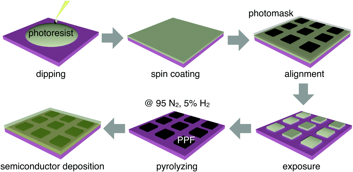 | ||
| Fig. 1 Schematic drawing of the fabrication process of the patterned PPF electrodes. | ||
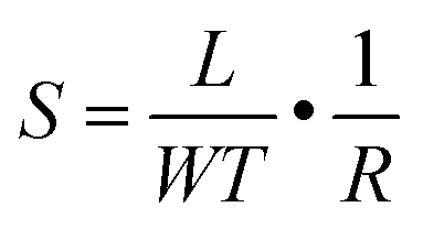
The surface morphology, film thickness, and electrical properties of the as-fabricated PPF electrodes were characterized by various methods. As shown in Fig. 2a, the electrode pattern obtained by photolithography has a size of 200 × 200 μm. The PPF surface roughness is determined by the AFM test in Fig. 2b. Compared with other carbon electrode surfaces, the PPF film has an atomic flat surface with less than 0.5 nm root mean square roughness and no defects or holes are introduced during the pyrolysis process. The thickness of the electrodes measured from the AFM image is 35 nm in Fig. 2c. The conductivity of the PPF electrodes is obtained through a two-terminal measurement. Two 120 nm thick gold electrodes are transferred onto one PPF electrode, as shown in Fig. 2d. Then, a current–voltage (I–V) curve is probed though the two gold electrodes. The resulting I–V curve is linear, representing an ohmic conductive behavior of the PPF electrode. By linear fitting of the I–V curve, the resistance (R) of the PPF electrode between the two gold electrodes is obtained. The electrical conductivity (S) can then be calculated by:
 | (1) |
 | ||
| Fig. 2 (a) Optical image of the 200 × 200 μm patterned electrode obtained by lithography. (b) AFM image of the carbon film electrode with surface roughness <0.5 nm. (c) AFM image of one PPF electrode. The thickness of the PPF electrode is measured to be 35 nm from the gap on the thin film. (d) Two-terminal I–V measurement for the calculation of the conductivity of the PPF electrode. The inset shows the schematic drawing of two gold electrodes deposited on one PPF electrode. (e) Surface potential images of the PPF surface measured by KPFM. (f) XPS spectra of the PPF films. | ||
We use XPS to further explore the chemical composition of the PPF thin film (Fig. 2f). The spectrum for PPF shows the presence of carbon C1s as a dominant peak (285 eV, 92%), and oxygen O1s (533 eV, 8%). The ratio of oxidized carbon to total carbon is equal to 0.08 for PPF. Oxygen functional groups are commonly detected on PPF substrates. The fresh samples after annealing at 1000–1100 °C under H2/N2 forming gas are proven the best with low O/C ratios of approximately 0.03 as previously reported.26 It is possible to identify several components from the high-resolution C1s core level spectra. A major component at 285 eV corresponds to C–C or C–H carbons. In addition, a variety of different surface oxygen functional groups are detected, such as C–OH groups at 286.5 (±0.3) eV, C![[double bond, length as m-dash]](https://www.rsc.org/images/entities/char_e001.gif) O in surface aldehydes and ketones at 287.8 (±0.3) eV and acid carboxylic groups at 289.3 (±0.3) eV. The atomic flat PPF electrodes with good conductivity are ready for OFET device applications.
O in surface aldehydes and ketones at 287.8 (±0.3) eV and acid carboxylic groups at 289.3 (±0.3) eV. The atomic flat PPF electrodes with good conductivity are ready for OFET device applications.
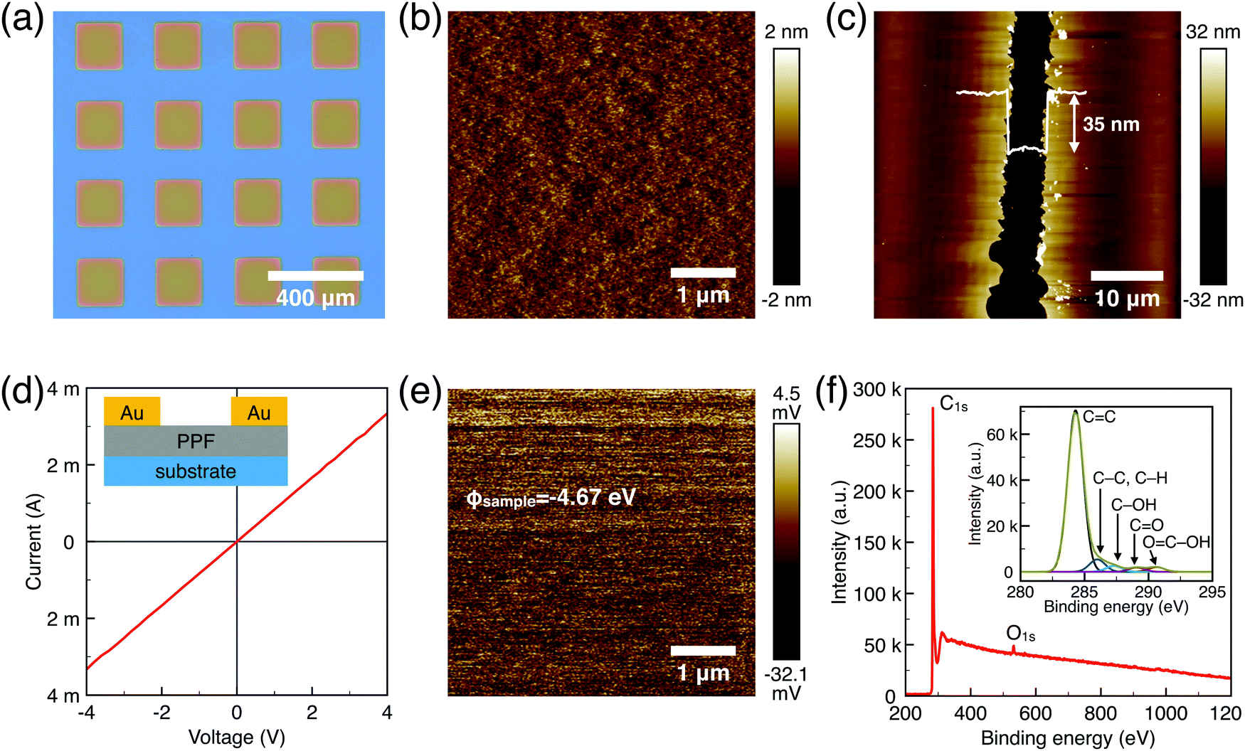
In bottom contact OFETs, the organic semiconductors are simultaneously deposited on both the channels and source/drain electrodes. Thus, the morphological discontinuity of the organic semiconductors deposited on the channels and source/drain electrodes could prevent charge carrier injection and increase contact resistance.27,28 Therefore, it is necessary to study the morphologies of DNTT on the channel and electrode regions. The optical image of the DNTT organic field-effect transistor is shown in Fig. 3a. As shown in Fig. 3b, the DNTT molecules adopt a relatively ordered packing structure on the carbon surface. When the DNTT grows on the low-surface-energy carbon surface, the interconnection between grains occurs and gradual lateral growth of grains fills the vacant space between grains. Any modifications at this interface can have a significant impact on the OFET device performance.29,30 SAMs based on trichlorosilane or phosphoric acid anchor groups have demonstrated a dramatic effect on the charge carrier mobilities in OFET devices, mainly by tuning the surface energy of the oxides.31,32 Here, we use octyltrichlorosilane (OTS) to modify the silica surface.29 And these crystal grains exhibit round or oval shape, as shown in Fig. 3c. Fig. 3d suggests that at the edge of the PPF electrode, the DNTT shows a continuous transition of morphology from Fig. 3b to Fig. 3c without apparent gaps or voids, ensuring a fluent charge transport in the lateral direction.
 | ||
| Fig. 3 (a) Optical image of bottom contact DNTT OFETs. (b) AFM morphology of DNTT deposited on the PPF electrode surface. (c) AFM morphology of DNTT deposited on the OTS modified SAM. (d) AFM morphology of DNTT deposition at the boundary between the electrode and dielectric layer. | ||
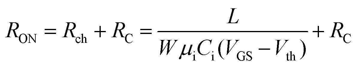
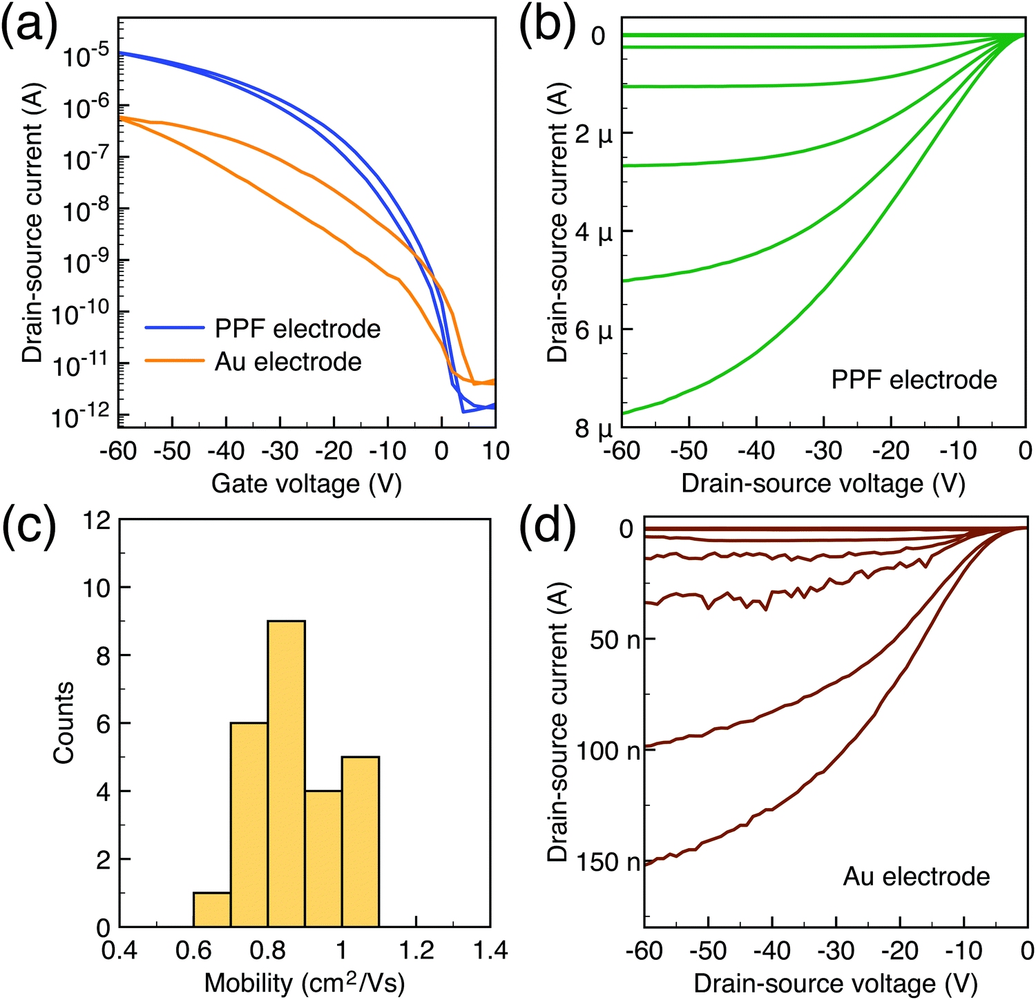
To characterize the device performance, we measure the transfer I–V curve of the bottom contact PPF electrode OFETs with DNTT as the semiconductor, as shown in Fig. 4a. The OFET based on the bottom contact gold electrode is also fabricated as the control sample. The on/off current ratio of the OFET devices is nearly 107. The threshold voltage obtained from linear fitting is −12.5 V, and the saturation field-effect mobility is 1.09 cm2 V−1 s−1. The output I–V curve is shown in Fig. 4b; there is non-linear I–V behavior at the small VDS region, indicating the presence of a charge injection barrier. To check for device variations, 25 devices were measured with an average mobility of 0.88 cm2 V−1 s−1. As a comparison, the device with a gold bottom electrode shows worse performance under the same experimental conditions (Fig. 4a). The saturation current drops over one order of magnitude, and the mobility is around 0.06 cm2 V−1 s−1. The output I–V curves exhibit more pronounced nonlinear behavior, as shown in Fig. 4d. The main performance reduction is attributed to the poor charge injection induced by bottom contact gold electrodes. To quantitatively judge the performance of carbon electrodes, we measured the contact resistance (RC) of the carbon electrode OFET by using the transfer line method (TLM). A set of devices with L ranging from 80 μm to 160 μm and a fixed W = 200 μm was used to calculate the RC at a low VDS of −5 V for various VGS, as described in eqn (2):
 | (2) |
 | ||
| Fig. 4 (a) Transfer I–V curve of DNTT transistors based on PPF and Au electrodes. (b) Output I–V curve of DNTT transistors based on PPF electrodes; the VG voltage step is 10 V. (c) Mobility histogram of 25 devices. (d) Output I–V curve of DNTT transistors based on Au electrodes; the VG voltage step is 10 V. | ||
 | ||
| Fig. 5 (a) Transfer I–V of carbon-based OFETs; (b) contact resistance of carbon-based OFETs at various VG; (c) transfer I–V of Au-based OFETs; (d) contact resistance of Au-based OFETs at various VG. | ||
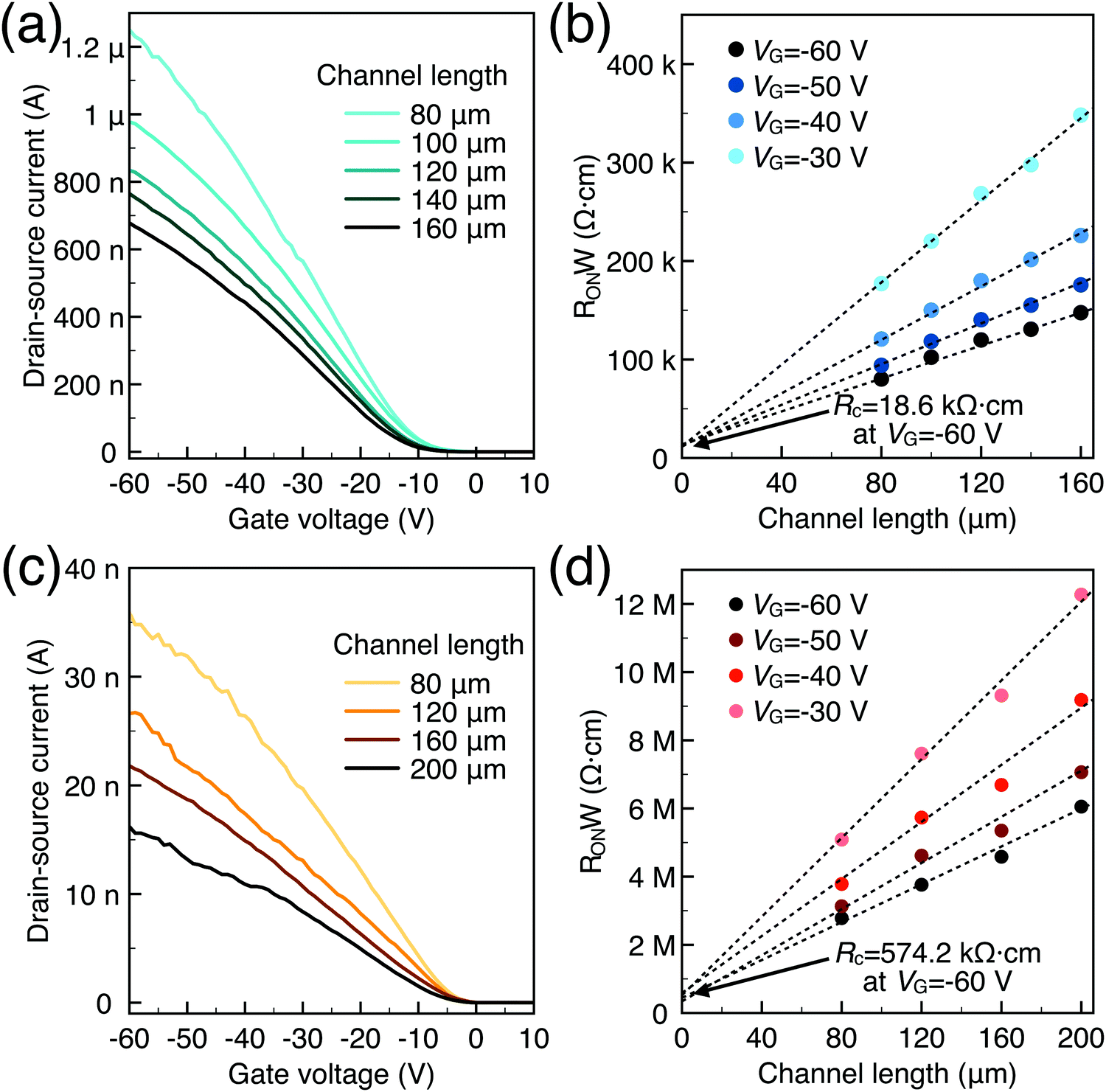
Generally, for an OFET device, the contact resistance is primarily caused by the charge-injection barrier at the interface between the electrode and semiconductor. The height of the barrier mainly depends on the work function difference of the two materials.6,33 For inorganic transistors like single-crystalline silicon MOSFETs, the barrier between the source/drain contacts and the semiconductor is modified by selectively doping the contact area. In OFETs, the barrier height can be reduced by selecting an electrode material with a work function that matches the LUMO or HOMO energy of the organic semiconductor. While the work function of PPF electrodes is lower than that of gold thin film in a vacuum but shows better injection properties. We speculated that the interface dipole between the electrode and semiconductor also plays an important role to determine the actual injection barrier height. To verify this, we explore the band structure of the DNTT/Au and DNTT/PPF interfaces by using in situ ultraviolet photoelectron spectroscopy (UPS), which is the most direct and quantitative measurement to investigate interfacial electronic structures. In Fig. 6a and b, we demonstrated the change of the UPS spectra of clean PPF by depositing increasing amounts of DNTT. The light source is a He1 discharge of hν = 21.2 eV. Fig. 6a is the secondary electron cut-off (SECO), which represents the vacuum level and is related to the position of the work function, and Fig. 6b is the valence-band photoelectron spectra, in which the onset of the first peak represents the highest occupied molecular orbital (HOMO). By depositing DNTT, the emission from the PPF substrate becomes suppressed and the spectrum is changed to that of DNTT.
 | ||
| Fig. 6 (a) SECO spectra and (b) valence region of DNTT deposited on carbon for increasing coverage by the UPS. (c) Schematic energy level diagram of the DNTT/carbon interface. (d) SECO spectra and (e) valence region of DNTT deposited on Au for increasing coverage by the UPS. (f) Schematic energy level diagram of the DNTT/Au interface. | ||
The work function of carbon is determined at 4.65 eV obtained from UPS data, which is very close to the result obtained by KPFM. At the initial stage to deposit 1.5 nm DNTT, the surface work function shows a shift up of 0.14 eV, which is increased with the well-known numerous interfacial phenomena, such as charge transfer and rearrangement, bond formation, and electron tail push-back in the actual interface. With the increasing deposing thickness, the vacuum level shifts back, representing the bulk properties of DNTT. And the HOMO peaks become more and more clear with increasing DNTT thicknesses and the shift from the Fermi edge of PPF gives the relative hole injection barrier. With an interfacial dipole, the hole-injection barrier is determined as eqn (3):
| ϕh = EI − ϕm − Δ | (3) |
Similarly, the UPS data and corresponding band structure of the DNTT/Au interface are shown in Fig. 6d–f. There is a large interface dipole that lowers the vacuum level by 0.36 eV. The injection barrier height calculated by eqn (3) is 0.74 eV owing to the significant Δ. Compared to DNTT/Au contact, the injection barrier is lower for the PPF electrode even if it has a lower work function. Therefore, it can be concluded that a better contact was formed for DNTT/PPF than for DNTT/Au because of the favorable orientation of the interfacial dipoles at the DNTT/PPF interface, which resulted in a lower hole-injection barrier. In addition, PPF is an amorphous carbon material with numerous active sites, which is expected to induce a strong interaction with DNTT by chemisorption and to form excellent interfacial contact. The UPS results provide direct evidence that the charge injection for DNTT/PPF is better than that for the DNTT/Au contact. These findings enhance the understanding that the value as well as the orientation of the interface dipole between the electrodes and semiconductor plays a critical role to determine the charge injection barrier height.
Conclusions
In summary, we have demonstrated that the performance of DNTT OFETs was significantly improved by using amorphous carbon material electrodes instead of conventional evaporated metal electrodes. Through detailed characterizations of the carbon and DNTT interface, key parameters such as the charge-injection barrier height were determined. The formation of a favorable interfacial dipole layer at the PPF-DNTT interface was shown to be the main reason for the improved performance of DNTT OFETs with carbon electrodes. This finding is beneficial to reducing the contact resistance of the OFET device, which is known as the bottleneck to further scale down the device for high frequency applications.Author contributions
X. Y., and X. C. R. conceived the idea, C. C. H., and X. H. D. prepared the carbon electrodes, C. C. H. fabricated the device, C. C. H., and X. H. D. performed the XPS and UPS measurements, C. C. H., and X. H. D. wrote the manuscript and discussed with all authors, X. Y., and W. P. H. directed and supervised the project.Conflicts of interest
There are no conflicts to declare.Acknowledgements
This work was supported by the National Natural Science Foundation of China (Grants 21773169 and 21973069), the Peiyang Young Scholars Program of Tianjin University (Grant 2018XRX-0007) and the Industry-University-Research Cooperation Program of Tianjin University and Qinghai Nationalities University (2021XZC-0064).References
- M.-J. Spijkman, K. Myny, E. C. P. Smits, P. Heremans, P. W. M. Blom and D. M. de Leeuw, Adv. Mater., 2011, 23, 3231–3242 CrossRef CAS PubMed
.
- E. Cantatore, T. C. T. Geuns, G. H. Gelinck, E. van Veenendaal, A. F. A. Gruijthuijsen, L. Schrijnemakers, S. Drews and D. M. de Leeuw, IEEE J. Solid-State Circuits, 2007, 42, 84–92 Search PubMed
- K. Myny, S. Steudel, P. Vicca, M. J. Beenhakkers, N. A. J. M. van Aerle, G. H. Gelinck, J. Genoe, W. Dehaene and P. Heremans, Solid-State Electron., 2009, 53, 1220–1226 CrossRef CAS
- M. E. Roberts, S. C. B. Mannsfeld, N. Queralto, C. Reese, J. Locklin, W. Knoll and Z. Bao, Proc. Natl. Acad. Sci. U. S. A., 2008, 105, 12134–12139 CrossRef CAS PubMed
- M. Waldrip, O. D. Jurchescu, D. J. Gundlach and E. G. Bittle, Adv. Funct. Mater., 2020, 30, 1904576 CrossRef CAS
- C. Liu, Y. Xu and Y.-Y. Noh, Mater. Today, 2015, 18, 79–96 CrossRef CAS
- S. Donnhäuser, M. Minagawa, S. Blawid and M. Claus, Solid-State Electron., 2020, 163, 107676 CrossRef
- P. Darmawan, T. Minari, A. Kumatani, Y. Li, C. Liu and K. Tsukagoshi, Appl. Phys. Lett., 2012, 100, 013303 CrossRef
- J.-L. Hou, D. Kasemann, J. Widmer, A. A. Günther, B. Lüssem and K. Leo, Appl. Phys. Lett., 2016, 108, 103303 CrossRef
- P. Darmawan, T. Minari, Y. Xu, S.-L. Li, H. Song, M. Chan and K. Tsukagoshi, Adv. Funct. Mater., 2012, 22, 4577–4583 CrossRef CAS
- S. Li, D. Guérin and K. Lmimouni, Microelectron. Eng., 2018, 195, 62–67 CrossRef CAS
- P. Stoliar, R. Kshirsagar, M. Massi, P. Annibale, C. Albonetti, D. M. de Leeuw and F. Biscarini, J. Am. Chem. Soc., 2007, 129, 6477–6484 CrossRef CAS PubMed
- D. J. Gundlach, L. Zhou, J. A. Nichols, T. N. Jackson, P. V. Necliudov and M. S. Shur, J. Appl. Phys., 2006, 100, 024509 CrossRef
- L. Diao, C. Daniel Frisbie, D. D. Schroepfer and P. Paul Ruden, J. Appl. Phys., 2007, 101, 014510 CrossRef
- S. Lee, G. Jo, S.-J. Kang, G. Wang, M. Choe, W. Park, D.-Y. Kim, Y. H. Kahng and T. Lee, Adv. Mater., 2011, 23, 100–105 CrossRef CAS PubMed
- X. Chen, S. Zhang, K. Wu, Z. Xu, H. Li, Y. Meng, X. Ma, L. Liu and L. Li, Adv. Electron. Mater., 2016, 2, 1500409 CrossRef
- R. L. McCreery, Chem. Rev., 2008, 108, 2646–2687 CrossRef CAS PubMed
- X. Mao, G. C. Rutledge and T. A. Hatton, Nano Today, 2014, 9, 405–432 CrossRef CAS
- J. Pinson and F. Podvorica, Chem. Soc. Rev., 2005, 34, 429 RSC
- A. Adenier, M. M. Chehimi, I. Gallardo, J. Pinson and N. Vilà, Langmuir, 2004, 20, 8243–8253 CrossRef CAS PubMed
- C. Wang, Y. Hou, J. Cheng, M.-J. Lin and X. Wang, Appl. Catal., B, 2021, 294, 120259 CrossRef CAS
- C. Fairman, S. S. C. Yu, G. Liu, A. J. Downard, D. B. Hibbert and J. J. Gooding, J. Solid State Electrochem., 2008, 12, 1357–1365 CrossRef CAS
- O. J. A. Schueller, S. T. Brittain, C. Marzolin and G. M. Whitesides, Chem. Mater., 1997, 9, 1399–1406 CrossRef CAS
- R. Kostecki, B. Schnyder, D. Alliata, X. Song, K. Kinoshita and R. Kötz, Thin Solid Films, 2001, 396, 36–43 CrossRef CAS
- S. Ranganathan and R. L. McCreery, Anal. Chem., 2001, 73, 893–900 CrossRef CAS PubMed
- M. Cortés, H. Smida, C. Mériadec, F. Barrière and C. Lagrost, Electrochem. Commun., 2017, 75, 48–51 CrossRef
- B. Peng, K. Cao, A. H. Y. Lau, M. Chen, Y. Lu and P. K. L. Chan, Adv. Mater., 2020, 32, 2002281 CrossRef CAS PubMed
- S. Braun, W. R. Salaneck and M. Fahlman, Adv. Mater., 2009, 21, 1450–1472 CrossRef CAS
- S. Y. Yang, K. Shin and C. E. Park, Adv. Funct. Mater., 2005, 15, 1806–1814 CrossRef CAS
- Y. Ito, A. A. Virkar, S. Mannsfeld, J. H. Oh, M. Toney, J. Locklin and Z. Bao, J. Am. Chem. Soc., 2009, 131, 9396–9404 CrossRef CAS PubMed
- H. Ishii, N. Hayashi, E. Ito, Y. Washizu, K. Sugi, Y. Kimura, M. Niwano, Y. Ouchi and K. Seki, Phys. Status Solidi A, 2004, 201, 1075–1094 CrossRef CAS
- D. Braga and G. Horowitz, Adv. Mater., 2009, 21, 1473–1486 CrossRef CAS
- R. T. Tung, Phys. Rev. Lett., 2000, 84, 6078–6081 CrossRef CAS PubMed
| This journal is © The Royal Society of Chemistry 2022 |