
 Open Access Article
 This Open Access Article is licensed under a Creative Commons Attribution-Non Commercial 3.0 Unported Licence
Polymer source-gated transistors with low saturation voltage
S.
Georgakopoulos†
 ,
R. A.
Sporea
and
M.
Shkunov
*
,
R. A.
Sporea
and
M.
Shkunov
*
Advanced Technology Institute, Electrical and Electronic Engineering, University of Surrey, Guildford GU2 7XH, UK. E-mail: m.shkunov@surrey.ac.uk
First published on 18th December 2021
Abstract
A type of injection-limited transistor is demonstrated with a conjugated polymer semiconductor and fluoropolymer insulator. The source-gated transistor (SGT) is based on a source Schottky barrier, the effective height of which is controlled by the gate voltage, shifting the origin of current modulation from the channel to the source-semiconductor contact. SGTs fabricated in this work saturate at up to 30 times lower drain voltages than FETs at high gate voltages. Saturation in SGTs is retained for short channels without requiring downscaling of the insulator layer. As the transistor channel has reduced influence on current modulation, the SGT output current is only weakly dependent on the channel length contrary to traditional FETs. These features come at some current reduction due to the series resistance stemming from the source depletion region. The ability to function with thick insulators, low voltage operation and thus low power consumption, as well as the reduced sensitivity to channel length variations could be highly synergistic with printing techniques used to deposit materials in organic electronics.
1. Introduction
The field-effect transistor (FET) is a widely used transistor type in organic electronics that utilises a gate voltage to modulate the charge flow between ohmic source and drain electrodes. An efficient p-type FET requires the source electrode workfunction to be close enough to the Ionization Potential (IP) of the semiconductor to allow the injection of holes. In the case of insufficiently high workfunction, a Schottky barrier is formed, reducing the transistor output current exponentially with the height of the barrier as demonstrated by numerous studies.1–4 While the loss of current is generally considered undesirable, the introduction of a source barrier can give rise to other characteristics that are very desirable.In p-type FETs commonly used with organic semiconductors, current modulation is achieved by biasing the gate-semiconductor capacitor with a voltage VG, resulting in charge accumulation and thus change in resistivity along the transistor channel. Upon the application of a drain–source voltage VD the accumulated charge flows, and for higher drain voltages (VD > VSAT, where VSAT -saturation voltage) the drain end of the channel is depleted of charge and the current saturates. The saturation voltage scales almost linearly with the gate voltage (VSAT ≈ VG–VT, where VT is the threshold voltage). For saturation to be strong, i.e. “flat” output characteristics above VSAT, the insulator thickness must be significantly smaller than the channel length (long channel rule), which imposes a design constraint. Although organic FETs with ultrathin insulators have been demonstrated,5 practical polymer dielectrics and high throughput processes associated with printed electronics usually require higher thicknesses to avoid gate leakage.6
The concept of source-gated transistors (SGTs) was introduced by Shannon and Gerstner based on amorphous silicon.7 SGTs structurally resemble FETs but rely on two primary conditions: (1) a source-semiconductor barrier, (2) the semiconductor layer must be sandwiched between the source and the insulator/gate, as in the case of a bottom-contact top-gate FET with the gate overlapping with the source electrode. This source-semiconductor-insulator-gate stack allows part of the gate voltage to drop across the semiconductor and effectively pull down the source barrier at the edge of the source electrode closest to the drain by image force lowering, allowing the injection of charge by thermionic-field emission.8 Additionally it is beneficial for the source electrode not to be excessively short, as there is an interplay of charge injection from the edge of the source and from the source-semiconductor interface further away from the edge, which can have an effect on device properties.9 Consequently, the transition from a channel-modulated operating regime in FETs, to a source-modulated regime in SGTs, considerably changes transistor behaviour and gives rise to useful features as discussed later on.
So far, the features of SGTs have not been associated with polymeric semiconductor transistors. Although it is well known that contact effects play a major role in organic FET operation.10 These effects have been explored extensively, e.g.11 lead to inadvertent SGT-like behaviour.12 Copper-rubrene contacts in bottom-gate, bottom-contact transistors have been shown to exhibit source barrier induced early saturation, (explained later on) however as one of the aforementioned SGT conditions of semiconductor positioned between the source and the gate insulator is not met, no current modulation is observed.13 Although output characteristics resembling SGTs have appeared in transistor contact effects studies, the authors have not explicitly recognized the operating mechanism and features of SGTs.3,14
In this work, structurally identical conjugated polymer transistors were fabricated (Fig. 1a) and engineered to display field-effect or source-gating behaviour by varying the effective electrode workfunction by up to 1.1 eV. We take advantage of high ionization potential (IP) polymer semiconductor to allow sufficient energy difference between electrodes workfunction and IP to tune the injection barrier. We examine the influence of estimated source barrier height on transistor current output and saturation behaviour, as well as describe the source-depletion induced saturation mechanism proposed by Shannon and Gerstner15 and validated by Valletta et al.,16 and assess its validity for organic SGTs made in this work.
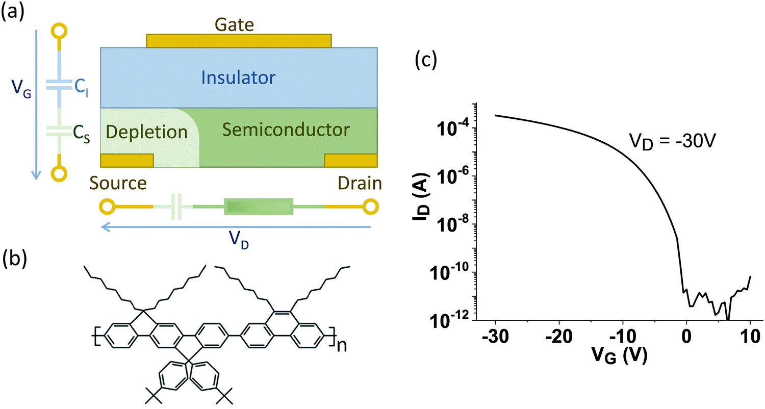 | ||
| Fig. 1 (a) Schematic of bottom-contact top-gate structure used for transistors in this work. (b) Chemical structure of poly(indenofluorene-phenanthrene) semiconductor. (c) Transfer characteristic of a polymer FET with near-ohmic source/drain electrodes, with channel length 5 μm, and channel width W = 1 cm. | ||
2. Transistor fabrication and barrier height estimation
Transistors were produced in the bottom-contact, top-gate configuration, with overlapping gate and source/drain electrodes. Bare Au (30 nm) and Cr/Au (3 nm/30 nm) electrodes were patterned on glass substrates by evaporation, photolithography, and I:KI:H2O etching for Au, and perchloric acid-cerium ammonium nitrate etching (Microchem MS8) for Cr. Bare Cr (30 nm) electrodes were DC magnetron sputtered and processed similarly. Au electrodes were cleaned by short exposure to O2 plasma (1 min, 75 W, 30 mL min−1) and treated with self-assembled monolayers pentafluorobenzene-thiol (PFBT) or fluorobenzene-thiol (FBT) in ethanol (1 mMol, 20 min immersion) to be able to vary the effective electrode workfunction.Poly(indenofluorene-phenanthrene) (PIFPA) co-polymer (Fig. 1b) is an amorphous, high ionization potential, air-stable semiconductor, with high field-effect peak saturation mobility of holes of 0.3 cm2 V−1 s−1![[thin space (1/6-em)]](https://www.rsc.org/images/entities/char_2009.gif) 17 (calculated from FET transfer characteristics in Fig. 1c). The amorphous morphology allows focus on the effect of contacts on device performance without worry for morphological variations due to the crystallisation of the semiconductor. The field-effect mobility was calculated by the standard MOSFET model as described elsewhere.18 PIFPA17 was spin-coated from anhydrous toluene solution (7.5 mg mL−1) with film thicknesses ranging from 30 nm to 100 nm, followed by annealing on a hotplate (100 °C, 5 min). The CytopTM fluoropolymer insulator was used as a gate dielectric due to its strong moisture barrier properties and low relative permittivity (εr = 2.1), that is critical for low energetic disorder along the interface with the semiconductor.19–21 CytopTM was deposited by spin-coating and annealed (100 °C, 10 min). For the top gate, 30 nm thick Au was thermally evaporated through a shadow mask. Fabrication and characterization were performed in ambient conditions. Electrical characterization was performed with a Keithley SCS-4200.
17 (calculated from FET transfer characteristics in Fig. 1c). The amorphous morphology allows focus on the effect of contacts on device performance without worry for morphological variations due to the crystallisation of the semiconductor. The field-effect mobility was calculated by the standard MOSFET model as described elsewhere.18 PIFPA17 was spin-coated from anhydrous toluene solution (7.5 mg mL−1) with film thicknesses ranging from 30 nm to 100 nm, followed by annealing on a hotplate (100 °C, 5 min). The CytopTM fluoropolymer insulator was used as a gate dielectric due to its strong moisture barrier properties and low relative permittivity (εr = 2.1), that is critical for low energetic disorder along the interface with the semiconductor.19–21 CytopTM was deposited by spin-coating and annealed (100 °C, 10 min). For the top gate, 30 nm thick Au was thermally evaporated through a shadow mask. Fabrication and characterization were performed in ambient conditions. Electrical characterization was performed with a Keithley SCS-4200.
The IP of PIFPA (5.79 eV) was measured by cyclic voltammetry (CV) on a Princeton Applied Research VersaSTAT 4.
Relative electrode workfunctions were measured with a McAllister Kelvin Probe KP6500 in air. All Kelvin Probe samples were treated similarly to transistor electrodes (etched and cleaned). A Cr thin film (same process parameters as for transistor electrodes) was used as a reference, and its workfunction was taken to be 4.5 eV22 to convert relative measurements to absolute workfunction values. Freshly evaporated Cr and etched/cleaned Cr samples exhibited negligible difference (0.02 eV). Measured relative workfunction values versus the Cr reference were: φAu+PFBT = φCr +1.08 eV, φCr/Au+PFBT = φCr +0.95 eV, φCr/Au+FBT = φCr +0.76 eV. Due to variations between successive measurements for Au electrodes, probably arising from humidity in the air, the error is estimated to be ±0.05 eV.
Source-semiconductor contact barrier heights were estimated by assuming vacuum level alignment of the semiconductor IP and measured electrode workfunctions. This assumption has been shown to be valid as long as the workfunction of the electrode lays at lower energies than the Fermi level of the semiconductor.23,24 It must be noted that the IP value measured by CV in this work is not likely to indicate the true position of the Fermi level in the semiconductor, as CV does not account for the relaxation of carriers to the positive polaron level. Polaron binding energies for organic semiconductors have been found to lay in the range of 0.4–0.7 eV.23,25,26 For electrodes with higher workfunction than the positive polaron energy, an interface dipole is formed, and the Fermi level of the electrode is pinned to the positive polaron level of the semiconductor,23,24 though this is not the case in this work.
The transistor currents measured in this work exhibit exponential decrease with increasing estimated barrier height in a clear trend as shown later. The estimated barrier heights are: Au-PFBT/PIFPA φB = 0.21 eV, Cr-Au-PFBT/PIFPA φB = 0.34 eV, Cr-Au-FBT/PIFPA φB = 0.53 eV, Cr/PIFPA φB = 1.29 eV. The exponential decrease in current still holds for the transition from φB = 0.34 eV to φB = 0.21 eV, indicating the lack of Fermi level pinning.
3. Results and discussion
The transfer characteristic of a polymer FET with near-ohmic contacts can be seen in Fig. 1c. The device has an effective field-effect mobility of 0.3 cm2 V−1 s−1 and near-zero threshold voltage, which does not change appreciably for SGTs. For Cytop gate film thickness of 1 μm the associated gate dielectric capacitance per unit area was calculated as 1.85 nF cm−2. The output characteristic for the same device can be seen in Fig. 2a. The saturation voltage scales strongly with VG. The current does not saturate well above the saturation voltage (dashed line in Fig. 2a). The reason for the lack of strong saturation is the specific geometry of this device, as the channel length is 5 μm and the insulator thickness 1 μm, i.e. the channel length is on the same order of magnitude as the insulator thickness and thus the long channel rule is not satisfied.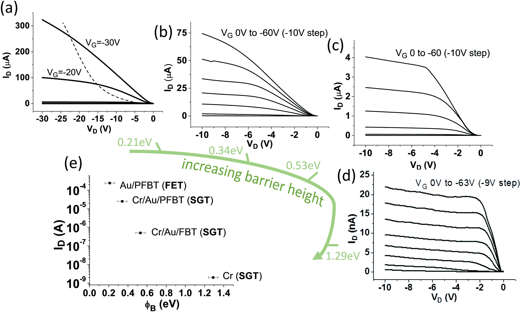 | ||
| Fig. 2 Output characteristics of (a) FET with near-ohmic Au-PFBT source/drain electrodes, with channel length L = 5 μm. The dashed line represents the transition into saturation regime. (b) Low barrier SGT with Cr/Au/PFBT electrodes, (c) medium barrier SGT with Cr/Au/FBT electrodes, d) high barrier SGT with Cr electrodes. Devices (b–d) have channel length L = 2.5 μm. Devices (a–d) have channel width W = 1 cm, insulator thickness di = 1 μm, source length 20 μm and varying semiconductor thicknesses. (e) Current output of different transistors at VG = −30 V and VD = −10 V, plotted against estimated barrier height φB. The current from 5 μm channel length FET was multiplied by a factor of 2 for channel length normalization. | ||
Fig. 2b–d displays output characteristics of SGTs of increasing barrier height. The source pinch-off can be clearly identified. The current is source modulated and thus it can be said that the devices are operating in the source-gating regime. The saturation voltage of the devices has decreased dramatically to several volts even for a VG of up to −60 V, as much as 30 times than an equivalent FET, and saturation is “flat” even though the channel is only 2.5 times longer than the insulator thickness, in violation of the long channel rule. The magnitude of the barrier affects the current level significantly (Fig. 2e) with the highest barrier of 1.29 eV resulting in a decrease of almost five orders of magnitude. It is very likely however that a middle ground can be attained where the current loss is minimised and the beneficial saturation behaviour retained.
To examine the saturation behaviour in more detail we will use the dielectric model. Under no external bias, the semiconductor area near the electrodes is partly depleted of charge due to the presence of Schottky barriers. Under a negative source–drain voltage, the drain Schottky barrier is forward-biased and its contribution assumed to be negligible. The source Schottky barrier is reverse-biased, and an increasingly negative drain voltage forces the depletion to extend towards the semiconductor-insulator interface, eventually pinching off the conduction channel and saturating current flow. As the semiconductor near the source is depleted, it can be treated as a dielectric in series with the insulator (Fig. 1a) to predict the change of potential across the source depletion region per unit VG. As any additional potential must be compensated by the drain voltage, this model predicts the rate of change of saturation voltage per unit volt applied on the gate (dVSAT/dVG). The dielectric model derived by Shannon and Gerstner for amorphous silicon SGTs states that the source–drain voltage at which current saturates (VSAT) can be expressed as (1)15 as opposed to FETs for which VSAT is given by (2):
 | (1) |
 | (2) |
According to the dielectric model, the gate voltage dependence of the saturation voltage can be finely tuned by adjusting semiconductor/insulator layer thicknesses. To assess its validity, Cr/PIFPA SGTs were produced with semiconductor thicknesses in the range of 30 to 100 nm, and insulator thicknesses in the range of 0.66 to 1.66 μm. Layer thicknesses were measured by profilometry (Tencor Alphastep 200) and tapping mode Atomic Force Microscopy (Veeco dimension 3000). Layer capacitances per unit area were calculated with relative permittivity εr = 2.1 for the insulator (CytopTM data sheet) and εr = 3 for PIFPA (not measured – typical conjugated polymer value). Calculated capacitance values were in the range of 89 to 26 nF cm−2 for the semiconductor layers and 2.8 to 1.11 nF cm−2 for the insulator layers. Saturation voltages VSAT were extracted from output characteristics at the onset of saturation for each gate voltage, and the rate of change of saturation voltage per unit gate voltage dVSATdVG−1 was calculated from the derivative of measured values.
The devices with the lowest and the highest dVSATdVG−1 values are shown in Fig. 3a and b. The calculated dVSATdVG−1 values (symbols) from several more devices were plotted against insulator capacitance (x-axis) and dVSATdVG−1 values predicted by the gate voltage derivative of eqn (1) for calculated semiconductor capacitance values (solid lines) (Fig. 3c). All values are summarised in Table 1.
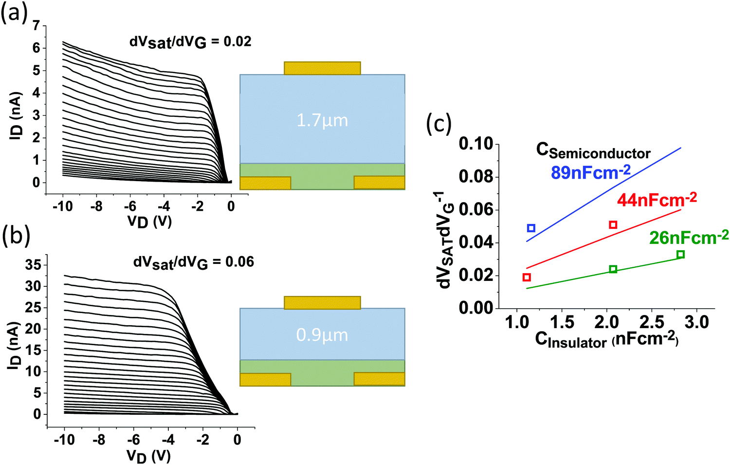 | ||
| Fig. 3 (a and b) Output characteristics of Cr/PIFPA SGTs, for VG = 0 V to −75 V (−3 V step). Characteristics correspond to devices fabricated with different combinations of semiconductor and insulator thicknesses dS and dI respectively. All channels have length L = 2.5 μm and width W = 1 cm. Device cross-section schematics illustrate different insulator thicknesses. (c) Experimental data (symbols) of high barrier (Cr/PIFPA) SGTs (5 devices) of different semiconductor and insulator layer thicknesses, plotted with dielectric model predictions of eqn (1) (solid lines). | ||
| Device | d S (nm) | d I (nm) | C S (nF cm−2) | C I (nF cm−2) | dVSATdVG−1 (measured) | dVSATdVG−1 (model) |
|---|---|---|---|---|---|---|
| (a) | 60 | 1680 | 44 | 1.10 | 0.019 | 0.025 |
| (b) | 30 | 900 | 89 | 2.05 | 0.024 | 0.022 |
| (c) | 60 | 900 | 44 | 2.05 | 0.051 | 0.045 |
| (d) | 100 | 1600 | 26 | 1.16 | 0.049 | 0.042 |
| (e) | 30 | 660 | 89 | 2.8 | 0.033 | 0.031 |
As seen in Fig. 3c the measured data conforms to the model very well. The observed dependence of dVSATdVG−1 on capacitance confirms the presence of a source depletion region responsible for the low-voltage channel pinch-off and saturation in SGT output characteristics.
We can estimate a difference in power consumption of an SGT – mode transistor versus Ohmic contact transistor. Considering that power dissipated by a single transistor is P = IDSAT × VDSAT, assuming negligible power loss at the gate, and using FET output data plots (Fig. 2) at comparable gate voltages, the following estimation can be made. Ohmic contact FET (Fig. 2a, VG = −20 V) will have power consumption of P(FET) ≈ 80 μA × 17.5 V ≈ 1.4 mW. Whereas source-gated transistor (Fig. 2d, VG = −27 V) will consume P(SGT) ≈ 5 nA × 1.7 V ≈ 8.5 nW, thus providing ∼1.6 × 10⁵ times lower power consumption. Even if we normalize the power figures by the current output to give watt-per-amp comparison, we still obtain an order of magnitude lower power consumption for SGTs (17.5 W A−1 for the FET and 1.7 W A−1 for the SGT) which is a direct result of the differences between eqn (1) and (2), i.e. SGT saturation voltage is significantly lower than the FET equivalent, though SGTs do have the disadvantage that a larger channel width could be required to obtain higher levels of current.
As the origin of modulation in SGTs has shifted from the channel to the source contact, the channel plays a much diminished role to current modulation. Simulations by two independent groups on amorphous silicon SGTs have shown that the current output can be independent of the channel length.27,28
Fig. 4a and b show the output characteristic of two SGTs with a channel length of 20 μm and 200 μm respectively and they exhibit nearly the same drain current. Fig. 4c shows data points from more measured transistors as a function of channel length. While not completely identical, the dependence of the current on channel length for SGTs is significantly weakened as compared to a hypothetical FET (dashed line). Such behavior could be highly beneficial for high-throughput printing techniques which may suffer from low electrode patterning resolution, enabling the production of functional low-cost circuitry.
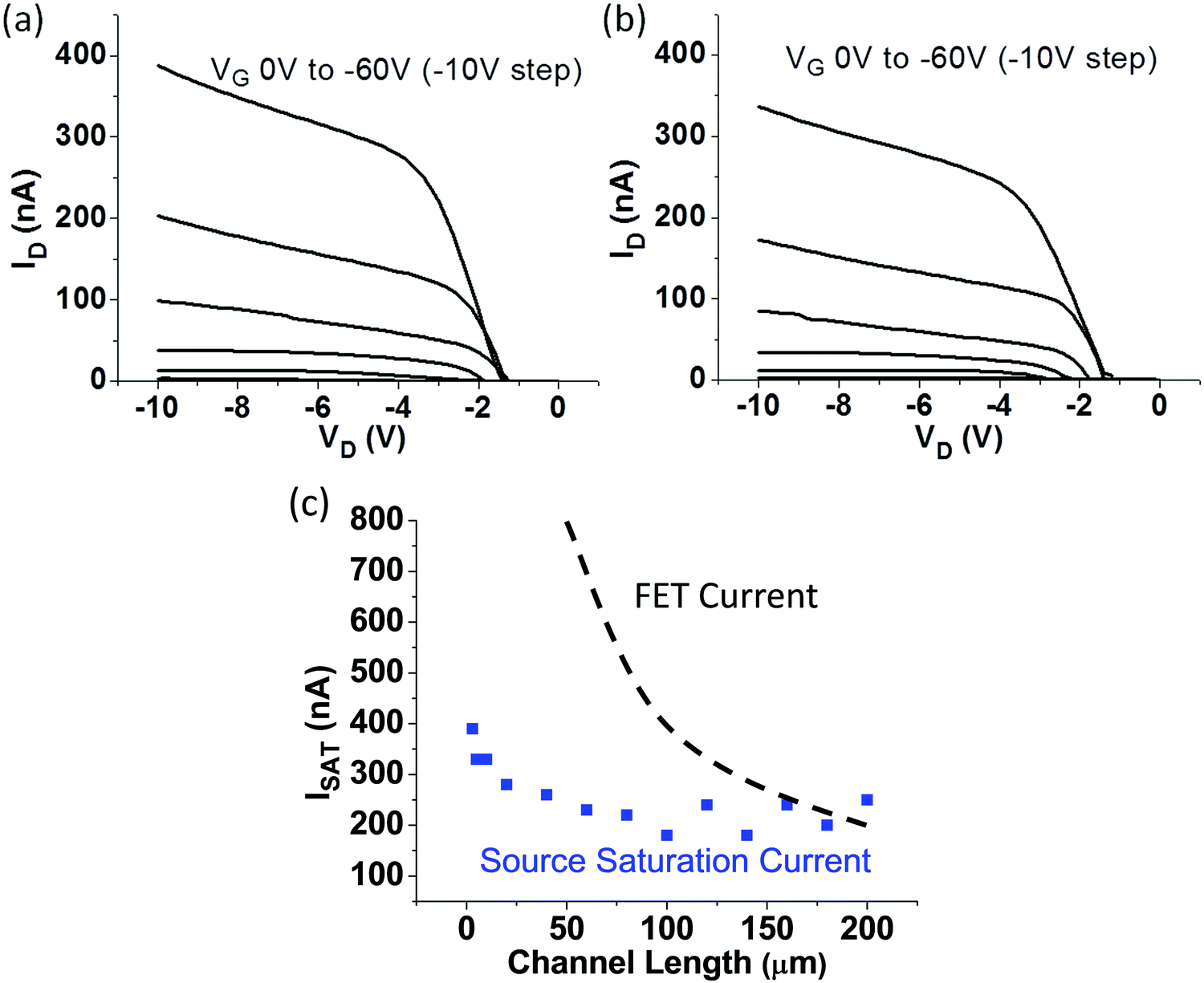 | ||
| Fig. 4 (a) Examples of output characteristics of high barrier SGTs with channel lengths (a) L = 20 μm and (b) L = 200 μm (c) currents extracted at the onset of saturation and VG = −60 V for transistors of different channel lengths. For this batch the gate leakage is moderate at low VD and drops off at increasing drain voltages. For other devices in this work gate leakage is negligible (below 1 nA) and is not shown. | ||
4. Conclusions
In summary, we have demonstrated SGTs based on conjugated co-polymer PIFPA. Fabricated organic SGTs exhibit saturation voltages up to 30 times lower than FETs. Strong saturation is maintained for short channels without requiring insulator downscaling as opposed to FETs. The source depletion mechanism that gives rise to the saturation was found to be valid by fitting experimental data to the dielectric model proposed by Shannon and Gerstner for amorphous silicon SGTs. Weak dependence of the current on channel length was observed. The current output of polymer SGTs was found to decrease exponentially with estimated barrier height, however it is possible to attain the source-gating characteristics with only one order of magnitude loss of current and perhaps even less with further optimisation.SGTs offer several opportunities for organic electronics. SGTs can be fabricated with semiconductors of high IP which are particularly attractive due to their excellent ambient stability, to which ohmic contacts may not be possible to establish. SGTs can be utilized in processes with short channel lengths and over-micron thick insulators, for example nanoimprinted source/drain electrodes and ink-jet or screen printed insulators. The insensitivity of SGT current output with channel length may be utilized with low-resolution electrode patterning techniques such as ink-jet printing. The significantly lower saturation voltage as compared to FETs should lead to lower power consumption as demonstrated with amorphous silicon SGTs.27,29 The high output impedance is ideal for analogue applications such as high-gain amplifiers30 and current sourcing.31
Conflicts of interest
There are no conflicts to declare.Acknowledgements
RAS would like to acknowledge financial support from EPSRC UK grant EP/V002759/1.References
- L. Bürgi, T. J. Richards, R. H. Friend and H. Sirringhaus, Close look at charge carrier injection in polymer field-effect transistors, J. Appl. Phys., 2003, 94, 6129–6137 CrossRef.
- B. H. Hamadani and D. Natelson, Nonlinear charge injection in organic field-effect transistors, J. Appl. Phys., 2005, 97, 064508 CrossRef.
- D. J. Gundlach, et al., An experimental study of contact effects in organic thin film transistors, J. Appl. Phys., 2006, 100, 024509 CrossRef.
- A. Bolognesi, A. D. Carlo and P. Lugli, Influence of carrier mobility and contact barrier height on the electrical characteristics of organic transistors, Appl. Phys. Lett., 2002, 81, 4646–4648 CrossRef CAS.
- L. A. Majewski, R. Schroeder and M. Grell, Organic field-effect transistors with ultrathin gate insulator, Synth. Met., 2004, 144, 97–100 CrossRef CAS.
- R. P. Ortiz, A. Facchetti and T. J. Marks, High-k Organic, Inorganic, and Hybrid Dielectrics for Low-Voltage Organic Field-Effect Transistors, Chem. Rev., 2010, 110, 205–239 CrossRef CAS PubMed.
- J. M. Shannon and E. G. Gerstner, Source-gated thin-film transistors, IEEE Electron Device Lett., 2003, 24, 405–407 CAS.
- F. Balon and J. M. Shannon, Analysis of Schottky barrier source-gated transistors in a-Si:H, Solid-State Electron., 2006, 50, 378–383 CrossRef CAS.
- R. A. Sporea, M. Overy, J. M. Shannon and S. R. P. Silva, Temperature dependence of the current in Schottky-barrier source-gated transistors, J. Appl. Phys., 2015, 117, 184502 CrossRef.
- H. Klauk, Will We See Gigahertz Organic Transistors?, Adv. Electron. Mater., 2018, 4, 1700474 CrossRef.
- L. Mariucci, et al., Current spreading effects in fully printed p-channel organic thin film transistors with Schottky source–drain contacts, Org. Electron., 2013, 14, 86–93 CrossRef CAS.
- K. Torikai, R. Furlan de Oliveira, D. H. Starnini de Camargo and C. C. Bof Bufon, Low-Voltage, Flexible, and Self-Encapsulated Ultracompact Organic Thin-Film Transistors Based on Nanomembranes, Nano Lett., 2018, 18, 5552–5561 CrossRef CAS PubMed.
- A. S. Molinari, et al., Quantitative analysis of electronic transport through weakly coupled metal/organic interfaces, Appl. Phys. Lett., 2008, 92, 133303 CrossRef.
- A. Valletta, et al., Contact effects in high performance fully printed p-channel organic thin film transistors, Appl. Phys. Lett., 2011, 99, 233309 CrossRef.
- J. M. Shannon and E. G. Gerstner, Source-gated transistors in hydrogenated amorphous silicon, Solid-State Electron., 2004, 48, 1155–1161 CrossRef CAS.
- A. Valletta, L. Mariucci, M. Rapisarda and G. Fortunato, Principle of operation and modeling of source-gated transistors, J. Appl. Phys., 2013, 114, 064501 CrossRef.
- S. Georgakopoulos, Y. Gu, M. Nielsen and M. Shkunov, Air-stable π-conjugated amorphous copolymer field-effect transistors with high mobility of 0.3 cm2 V−1 s−1, Appl. Phys. Lett., 2012, 101, 213305, DOI:10.1063/1.4767921.
- S. Georgakopoulos, D. Sparrowe, F. Meyer and M. Shkunov, Stability of top- and bottom-gate amorphous polymer field-effect transistors, Appl. Phys. Lett., 2010, 97, 243507 CrossRef.
- M. Uno, Y. Tominari and J. Takeya, Fabrication of high-mobility organic single-crystal field-effect transistors with amorphous fluoropolymer gate insulators, Org. Electron., 2008, 9, 753–756 CrossRef CAS.
- R. Hamilton, et al., High-Performance Polymer-Small Molecule Blend Organic Transistors, Adv. Mater., 2009, 21, 1166–1171 CrossRef CAS.
- J. Veres, S. D. Ogier, S. W. Leeming, D. C. Cupertino and S. Mohialdin, Khaffaf, Low-k Insulators as the Choice of Dielectrics in Organic Field-Effect Transistors, Adv. Funct. Mater., 2003, 13, 199–204 CrossRef CAS.
- D. E. Eastman, Photoelectric Work Functions of Transition, Rare-Earth, and Noble Metals, Phys. Rev. B: Solid State, 1970, 2, 1–2 CrossRef.
- C. Tengstedt, et al., Fermi-level pinning at conjugated polymer interfaces, Appl. Phys. Lett., 2006, 88, 053502 CrossRef.
- I. Lange, et al., Band Bending in Conjugated Polymer Layers, Phys. Rev. Lett., 2011, 106, 216402 CrossRef PubMed.
- A. Crispin, X. Crispin, M. Fahlman, M. Berggren and W. R. Salaneck, Transition between energy level alignment regimes at a low band gap polymer-electrode interfaces, Appl. Phys. Lett., 2006, 89, 213503 CrossRef.
- I. G. Hill, D. Milliron, J. Schwartz and A. Kahn, Organic semiconductor interfaces: electronic structure and transport properties, Appl. Surf. Sci., 2000, 166, 354–362 CrossRef CAS.
- T. Lindner, G. Paasch and S. Scheinert, Simulated operation and properties of source-gated thin-film transistors, IEEE Trans. Electron Devices, 2005, 52, 47–55 Search PubMed.
- F. Balon and J. M. Shannon, Modeling of Source-Gated Transistors in Amorphous Silicon, J. Electrochem. Soc., 2005, 152, G674 CrossRef CAS.
- J. M. Shannon and F. Balon, Source-gated thin-film transistors, Solid-State Electron., 2008, 52, 449–454 CrossRef CAS.
- E. Bestelink, et al., Compact Source-Gated Transistor Analog Circuits for Ubiquitous Sensors, IEEE Sens. J., 2020, 20, 14903–14913 CAS.
- R. A. Sporea, M. J. Trainor, N. D. Young, J. M. Shannon and S. R. P. Silva, Intrinsic Gain in Self-Aligned Polysilicon Source-Gated Transistors, IEEE Trans. Electron Devices, 2010, 57, 2434–2439 CAS.
Footnote |
| † Current address: Multifunctional Molecular Materials Group, Department of Organic Chemistry, University of Murcia, 30100 Murcia, Spain. |
| This journal is © The Royal Society of Chemistry 2022 |