Challenges and emerging opportunities in transistor-based ultrathin electronics: design and fabrication for healthcare applications

Ruomei Shao , Rui Ma , Xuyao An , Chunnan Wang and Shuqing Sun *
Institute of Biopharmaceutical and Healthcare Engineering, Shenzhen International Graduate School, Tsinghua University, Shenzhen 518055, China. E-mail: sun.shuqing@sz.tsinghua.edu.cn

Received 13th September 2021 , Accepted 24th November 2021

First published on 11th January 2022


Abstract

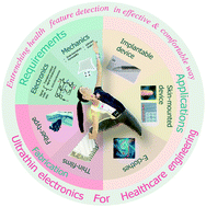
Ultrathin healthcare electronics are gradually being employed for daily physiological monitoring and medical treatment tasks which have long been dominated by bulk and expensive devices. Recent advances in ultrathin devices have enabled more intimate interactions between humans and electronics in a highly accurate, comfortable, and even imperceptible manner. However, demands for new paradigms to establish long-term biosafe, robust, and anti-interference devices for healthcare management are still increasing, particularly amid the coronavirus pandemic. This review summarizes the recent progress in ultrathin transistor-based wearable devices ranging from implantable, skin-mounted devices to smart textiles. Emerging solutions and promising strategies for challenges encountered by high-performance systems have been summarized comprehensively from both mechanical (such as strain-insensitivity and permeability) and electronic (such as signal transduction ability and anti-interference) perspectives. In addition, the design and fabrication of ultrathin electronics with different topological categories have been discussed in detail. The prospective applications for ultrathin electronics to integrate with sensors, perception components, actuators, and drug delivery for clinical or healthcare management have been summarized.


1. Introduction

Conventional bulky, rigid, and expensive clinical devices make continuous monitoring of the physiological parameters of outpatients very challenging. Thus, the development of lightweight and low-cost electronic devices with comfort has become an urgent need. To satisfy these requirements, ultrathin electronics (thickness of sub 300 μm) have been developed and have even ceaselessly advanced into wearable systems.1–6 The reduction in the thickness of devices could galvanize improvements in both flexibility and weight. The former delivers compliant mechanical properties that can match various surfaces of a 3D curved bio-morphology (e.g., examined pig skin with the roughness ranging from 1.9 to 90 nm to 240 μm7) and the low Young's modulus of biological surfaces (e.g., elastic moduli of neural tissues are approximately in the 100 to 1500 kPa range8), and the latter facilitates adhesion and further integration with the human body as a tissue- and skin-attachable material and even as a woven cloth with an imperceptible feel during usage.9 Moreover, as implantable devices, ultrathin electronic devices can also minimize the invasive reactions to realize long-term monitoring.10,11

Unlike traditional silicon-based rigid electronics, ultrathin transistor-based electronics and devices are mild, bio-safe, low-cost, and consume low energy. Benefiting from the advances in plastic sensors and organic transistors since the 1980s,12–14 organic semiconductor materials,15–18 dielectric materials,19–22 thin-film logic/analog circuits,23–27 radio-frequency identification (RFID) tags,28–31 and displays32,33 have been extensively explored. This has resulted in exciting and remarkable research being conducted, such as the development of devices with biocompatibility,4,34 transparency,35–37 self-healing properties38–40 and stretchability41–43 using ultrathin transistors, which interact more intimately with our body.

The exploration of the structural design and fabrication of ultrathin electronics is ongoing; however, emerging design requirements of ultra-flexibility, durability, and anti-interference of robustness, particularly under the emerging mechanical and electrical requirements as a new confluence, are yet to be realized. Surface-compliant films with 1D fibers or 2/3D patterns are considered essential for structural design44–47 (Fig. 1). The major electrical requirements for semiconductor materials are good conductivity with stretchability and high semicrystalline with uniformity. However, several critical challenges for electrical principles have also attracted attention, such as high signal-to-noise ratio (SNR) and anti-surrounding-interference performance (motion interruption, temperature, water, etc.). Moreover, to realize truly multifunctional sensing with motion recognition output, certain interdisciplinary tools, including classical analog amplification circuits, traditional machine learning algorithms, and deep learning networks, are in the process of collaborating toward high-level signal recording and processing.53 These principles and advances have been discussed later. However, regarding wearable devices, the exploration of ultrathin electronic integration systems for closed-loop information circling and self-power is still quite limited.54


image file: d1tc04384f-f1.tif
Fig. 1 General illustration of ultrathin electronics for a broad range of healthcare applications with a new paradigm and tendency. A stretching-insensitive ultrathin transistor-based temperature sensor with stretching-insensitive ability.48 Copyright 2018, Nature Publishing Group. Inflammation-free implantable nerve-probe devices.49 Copyright 2015, Wiley-VCH. A high-density skin-mounted sensor.50 Copyright 2021, AAAS. Electronic clothes with large-area ZnS display textiles.51 Copyright 2021, Springer Nature. An organic electrochemical transistor array for tissue-attachable materials.52 Copyright 2018, AAAS. Semiconductor films with a fiber-type nanoconfinement structure.42 Copyright 2017, AAAS.

In addition, there are several more emerging requirements for manufacturing at the system level of ultrathin devices.55,56 Furthermore, solution-based fabrication for large-scale and programmable processes has been proven to be effective.26,57,58 Moreover, room-temperature fabrication technology is in demand owing to the benefit of avoiding the shrinking issue of ultra-thin plastic substrates.54 However, the fabrication and assembly process of an integrated platform should be further discussed under the conditions of homogenous mechanical properties and electrical coupling.

Although there are many excellent reviews on healthcare devices,3,59–62 a comprehensive discussion of the recent paradigms and criteria is still lacking. This study provides a roadmap for the design and fabrication of ultrathin transistor-based electronics based on emerging confluences for long-term applications for healthcare monitoring as well as clinical diagnosis and therapeutics. In Section 2, we present the mechanical and electrical design strategies for the emerging requirements and properties of ultrathin electronics. In Section 3, we discuss and review the fabrication technology for various solution-based processes to address ultrathin structure considering 1-dimensional (1D) to multilayer geometric issues. In Section 4, to accommodate various surface and body dynamics, new principles and requirements for the design and fabrication of ultrathin electronics are gradually unfolded with different levels of close interactions between our body and a smart system, including e-fiber, smart cloth to e-skin, and implant devices. Furthermore, we describe the latest progress in ultrathin electronics that are classified into three levels depending on the interaction with the human body: (1) implantable devices, (2) skin-attachable devices, and (3) fiber and woven electronics for e-textiles. Finally, we provide future prospects in Section 5 focusing on the challenges and requirements to satisfy the increasingly larger demands and higher criteria of healthcare wearable devices.

2. Emerging concepts for mechanical and electrical designs of ultrathin electronics

As mentioned above, ultrathin electronics offer excellent advantages such as better wearable comfort, portability, and topographical compliance. Consequently, a wearable healthcare device should consider more advanced factors, including strain insensitivity, gas permeability, wash-resistant ability, high SNR, anti-interference (fluctuating extra electrical field, motion, temperature, water, or moisture), and other requirements (Fig. 2).
image file: d1tc04384f-f2.tif
Fig. 2 Emerging challenges and corresponding strategies for ultrathin healthcare devices.

2.1 New requirements for mechanical performance

2.1.1 Stretch-insensitivity. An ultrathin device must be compliant and robust. Several excellent reviews have referred to the topic of strain engineering. Good stretchability is vital for ultrathin devices for semiconducting components as well as conducting parts.63–69 It has been proven that a low Young's modulus results in much stronger ultrathin electronics under the conditions of flexible usage scenarios to achieve better fitness for complex bio-surfaces.70–73 However, a general survey on the principles of solutions is lacking. In fact, conventional manufacturing of flexible functional materials, including iontronic materials, liquid metals, and conductive polymers doped with micro-/nanoparticles, inevitably results in fluctuations in their conductivity because of strain.79–86 Hence, a thorough examination of strategies for stretch insensitivity is needed to better understand the aspects related to strain.

The reported strategies for stretch insensitivity can be classified into two categories: structural design including nano-patterning, micro-patterning, and electrical solutions, which have been reviewed in the next section.

First, an exciting example of a nano-patterned structure utilized composite materials based on vertically aligned conductive magnetic nanoparticles of an urchin shape (US-CMNPs)74 (see Fig. 3A). It comprises magnetic silver-nickel NP cores and was shelled with gold nano-needles. Herein, the chemical reduction method was chosen to synthesize the piezoresistive composite. The specially aligned structure was formed by a guiding magnetic field applied to a polyurethane elastomer doped with magnetic nanoparticles. Hence, the anisotropically arranged nanoparticles contribute to a large difference in sensitivity along each axis. Therefore, it greatly minimizes the strain sensitivity of the substrate.


image file: d1tc04384f-f3.tif
Fig. 3 Topological solutions for strain-insensitivity. (A) A stretchable tactile sensor with dynamic stability based on vertically aligned urchin-shaped nanoparticles.74 Copyright 2020, Elsevier Ltd. (B) A one-dimensional fiber-shaped structure for a stretchable electronic tandem.75 Copyright 2018, Springer Nature. (C) Monolithic stretchable electronics with a superelastic liquid–metal mat.76 Copyright 2021, Springer Nature. (D) A deformable nanowire transistor.77 Copyright 2018, Wiley-VCH. (E) An island-type train-insensitive intrinsically stretchable transistor array.78 Copyright 2021, Springer Nature.

Second, another solution is a micro-/nano-patterned structure, which can be divided into three categories: 1D fiber-shape, 2D film-shape and 3D topologies. In the case of 1D patterns, the fiber-shaped devices are mostly established by mounting a spring-like conductive fiber around a stretchable polymer core75,87,88 (Fig. 3B). It works similar to an old telephone coil, which can easily be prolonged without sacrificing its conductivity. Regarding 2D and 3D micro-/nano-topologies, further options have been provided recently, including serpentine structures, wavy patterns and porous patterns63,66,71,89–95 (Fig. 3C). In general, this type of architecture can offer additional deformation without destroying the intertwined conductive composites.76 However, to prevent cracks, delicate functional components are assembled with base materials to provide high mechanical stability.

The strain sensitivity of organic semiconducting materials is more complicated and depends on the degree of nucleation and its crystalline orientation as well as the alignment of organic semiconductors.54,96 In general, the stretching of thin-film semiconductors has negative impacts on the semiconductor crystalline structure. Therefore, significant degradation of the field-effect mobility and current output may occur.

Recent reports have addressed this challenge. The first is based on a nanoconfinement morphology42,77,97 (Fig. 3D). Nanoconfinement of polymers offers the advantages of a lower mechanical modulus and increased mechanical durability. In this system, a solution contains polystyrene-block-poly(ethylene-ran butylene)-block-polystyrene (SEBS) and poly(2,5–bis(2-octyldodecyl)-3,6-di(thiophen-2-yl)diketopyrrolo[3,4-c]pyrrole-1,4-dione-alt-thieno[3,2-b]thiophene) (DPPT_TT;1), each of which acts as an elastomer substrate and active semiconductor, respectively.42 By forming nanofibrils inside a deformable elastomer, a nanoconfinement structure of the polymer semiconductor was achieved. Consequently, owing to their comparative surface energy, nanoscale phase separation is generated along with the formation of the nanoconfinement morphology. Using a fiber-net-like semiconductor, the output of the current was demonstrated to be relatively steady at an elongation of 75%. Another reported strategy involves following the design of the reorganization of crystalline orientation and alignment.98 When combined with the strategies of nanoconfinement morphology and solution shearing by a microtrench blade array, the effect of semiconductor mobility increases three-fold with stable outputs while it is stretched by more than 100% of its length.

In addition, the “island-bridge” configuration serves as an alternative which is typically used to assemble silicon-based chips with a plastic substrate.99–102 However, owing to the difference in the mechanical modulus, a significant mismatch occurs between the rigid chip and compliant polymer. Furthermore, soft substrates suffer from most of the shear force and result in the formation of vulnerable points in the rigid-soft interface. Progress has been reported in the case of stretch-insensitive semiconductor circuits, based on following the “Island-bridge” principle, wherein the stiffness of semiconductor components was modified78 (Fig. 3E). In addition, the difference in modulus between the passive substrate and active “island” can reduce the share-straining-deformation in the latter by approximately four-fold at 100% of the entire strain. Consequently, strain insensitivity was achieved by less than 5% variation up to 100% strain.

2.1.2 Permeability. Regarding skin-attachable electronics, gas/sweat permeability is a major factor that affects long-term continuous monitoring without causing inflammation and discomfort.71,103–105 Furthermore, it also enables durable attachment by suppressing the interruption of sweat within the skin-electronics interface.

To solve this issue, a high-porosity structure should be considered as a fundamental approach. The porous structure must be carefully designed, including the size and line width, to avoid the possibility of blocking sweat glands (approximately 100 μm in diameter)71 (see Fig. 4A). In addition, it also results in the reduction of the modulus, instinctive stretchability, and larger contact area for both the dielectric-active and active-passive interfaces of skin-attachable devices.


image file: d1tc04384f-f4.tif
Fig. 4 Air-permeability for skin-attached electronics. (A) Nanomesh on-skin electronics.71 Copyright 2017, Springer Nature. (B) Demonstration of water permeability for a liquid–metal fiber mat.76 Copyright 2021, Springer Nature. (C) Enhanced breathability of on-skin electronics.103 Copyright 2020, Elsevier Ltd. (D) All-porous elastomer electronics.44 Copyright 2018, Wiley-VCH.

Recent progress in this regard comprises two approaches. One typical configuration is a stacked micro-/nano-fiber, which is generally obtained by spinning technology with active and passive polymer mixture solutions71,106,107 (see Fig. 4B). The other is 2D nanopatterning. Conductive nanomeshes can be obtained by photolithography, grain boundary lithography, and crack-patterned approaches via chemical vapor deposition (CVD) and other thin-film methods.64,66,69,108

Hydrophilia of skin-mounted gas/sweat-permeable films has been reported as another key factor in the enhancement of water transportation through nano-/micro-meshes103 (see Fig. 4C). Following a similar method with an additional monolayer of 1-thioglycerol molecules modified on the mesh surface, the sweat evaporation from the substrate-free electrodes was improved by a factor of 3.6. Moreover, without sacrificing its thickness, it maintains long-term conformity and flexibility with the skin.

In addition to substrate-free electronics, structural materials, which commonly refer to the dielectics of transistor-based devices and electrical package layers, are also required to be hollow patterned44,76,109,110 (see Fig. 4D). A typical example reported is a substrate material using a sugar-templated elastomer sponge to fabricate an all-gas-permeable device.44

2.1.3 Adhesion. The adhesion between electronics and tissue, electronics, and skin, as well as the inside of electronics, is another challenge in the research of flexible electrodes. Strong and comfortable adhesion approaches could pave the way for a longer lifetime of the product in the future.111,117,118 The adhesion between the stacking interlayers is a serious consideration for minimizing the peeling failure and reliability of electronic devices.111,114,119 In this case, the ultrathin characteristics of thickness, biocompatibility, and reversibility are greatly appreciated in the adhesion of bio-electronics.

First, ultrathin electronics are highly appreciated for healthcare monitoring because of their conformal ability and low Young's modulus to match 3D complicated biosurfaces. The thinner the device, the better it is.9 Tough adhesion of transistor-based electronics or organic photovoltaics with a thickness of sub-10 μm to tissue/skin without additional paste agent has been realized (Fig. 5A).120–122 In addition, sub-300 nm electronics are also described as imperceptible and demonstrate ultra-conformability to bio-surfaces9,71,112,123 (see Fig. 5B).


image file: d1tc04384f-f5.tif
Fig. 5 Photograph of adhesion. (A) Multilayered electronic transfer tattoo.111 Copyright 2021, AAAS. (B) 300-nm biocompatible e-skin.112 Copyright 2016, Wiley-VCH. (C) Tough bio-compatible adhesives on wet surfaces.113 Copyright 2017, AAAS. (D) Electrical bioadhesive interface.114 Copyright 2021, Springer Nature. (E) Photodetachable adhesion.115 Copyright 2019, Wiley-VCH. (F) Amphibians and octopi for omnidirectionally enhanced wet adhesion.116 Copyright 2019, Wiley-VCH. (G) Microlithography of high-density elastic circuits.50 Copyright 2021, AAAS.

Second, the epidermis of the tissue is a type of wet surface and adhesion on wet surfaces has already become a rising hot issue. However, several other complex and dynamic factors must also be considered, such as blood coagulation, anti-bleeding interference, and inflammation.52 Natural materials are good candidates for solutions to these difficult problems. Several groups have employed dopamine, a type of mussel-inspired natural adhesive.119 An intertwined topology adhesion network is formed via branched structures that are delicately designed to have a higher molecular weight, such as poly(ethylene glycol) diacrylate (Mw = 200). Furthermore, a silk-based sealant is demonstrated as a tough adhesion agent on bloody tissue with instant homeostasis and good biocompatibility.124

Moreover, an impressive report follows the principle of amidation between the amido and carboxyl groups.113 Owing to the abundant carboxyl groups in biological tissues, it greatly enhances the robustness and toughness of the tissue-electronics interface (Fig. 5C). In addition, the dissipative matrix is designed to effectively share the dissipating energy. Following the same fundamental principle, a type of dry double-sided tape for adhesion was developed.125 The mechanism of its quick adhesion ability (≤5s) is due to the dry dissipative block to absorb and remove the interfacial water layer on the surface, resulting in the exposed dry surface subsequently forming a strong covalent bond.

Reverse adhesion is a useful concept in bioelectronics. An e-bioadhesive method with reversible wet-surface adhesion between tissues and electronics has been reported114 (Fig. 5D). Based on the above-mentioned dry substrate and amidation reactions, graphene oxide was introduced into a poly(vinyl alcohol) (PVA) hydrogel composite as the conductive component, and further grafted with N-hydroxysuccinimide ester (PAA-NHS ester). The combined working principles involved are covalent bonding, hydrogen bonding, and electrostatic interactions. Another group reported photodetachable adhesion between hydrogels.115,126 The spreading long chains realized a strong entanglement on the adhesion interfaces. Furthermore, a third intertwined network via the Fe3+ complexation reaction facilitated reversible adhesion upon UV light exposure (Fig. 5E). Electrophoresis by electrically driven diffusion reactions has also induced a reversible effect on the adhesion of flexible materials. The introduction of external stimuli resulted in the formation of cationic–anionic bonds that follow electrically driven motions that can be disabled within a certain period of time.

Templated micro-patterned structures are also an efficient way of establishing adhesion for either dry or wet surfaces, termed dry adhesives. Many excellent studies have been reported following this approach as a biocompatible and bio-safe strategy.116,127–129 For example, based on the phenomenon of the Cassie state of a liquid droplet suspended on the head of micropillars, mushroom-shaped PDMS fibrillary arrays can effectively remove the water thin layer on the surface and accomplish adhesion to the contact interface.130 This method can also be applied to surfaces with low-surface-tension liquids, oil, and other liquids. Another group created an octopus-inspired nanosucker array to achieve a tough contact with tissue surroundings131(Fig. 5F). This templated PDMS structure also provides a promising solution for wound care.

Adhesion among electronic interlayers is another potential issue. Regarding thin-film electronics, the approaches commonly rely on van der Waals forces and electrostatic force.54 However, with an increase in structural complexity, the number of interlayers and interconnections of circuits, as well as the thickness of the device, increases correspondingly.

Consequently, the possibilities of adhesion failure, such as peeling off, become possible. In addition, the additional thickness introduces a mismatch between the inadequate binding force and the mechanical modulus.9 Representative approaches have been demonstrated using optical microlithography (UV irradiation) with the help of benzophenone and a carbine photoinitiator.50,134,135 Furthermore, UV-triggered reactions have been proven to be efficient for crosslinking between polymer chains and the fabrication of all-transparent sensor devices50 (see Fig. 5G).

2.1.4 Washability. E-textiles have evolved into an indispensable component of wearable devices.51,75,132,136,137 They provide multiple options to facilitate human–machine interfaces and additional daily monitoring of health, including body motions and physiological detections. The mechanical durability of woven e-textiles has recently garnered attention, particularly washability, which is found to be a natural property of traditional fabrics. However, this is still not a trivial issue for electronics.138,139 In addition, anti-abrasion must also be considered for E-cloth to facilitate its washability in washing machines.

Several groups have already attempted to overcome this challenge. Water-proof encapsulation was the first proposed idea. By using an ultrathin (1 μm) parylene passive film, the electrical performance of organic photovoltaics decreases by only 5.4% after dipping in water for 120 min (Fig. 6A).70 Regarding e-fiber, a core–shell structure was reported as washable, wherein the hydrogel core made of poly(2-acrylamido-2-methyl-1-propanesulfonic acid-co-acrylamide) hydrogel doped with conductive reduced-graphene-oxide was encapsulated by a thermochromic silicon elastomer (Fig. 6C).132


image file: d1tc04384f-f6.tif
Fig. 6 Washable electronic textiles. (A) Elastomer-coated organic photovoltaics.70 Copyright 2017, Springer Nature. (B) Large-area display textiles.51 Copyright 2021, Springer Nature. (C) Core–shell segmental hydrogel thermochromic elastomer hybrid fibers.132 Copyright 2020, American Chemical Society. (D) Waterproof triboelectric yarns based on Fermat's spirals.133 Copyright 2021, Wiley-VCH.

An excellent machine-washable large-area e-textile has recently been demonstrated for wearable display devices51,140 (Fig. 6B). It was fabricated by the encapsulation of ZnS phosphor slurry (with a diameter of approximately 0.3 mm), followed by drying at 120 °C. Consequently, the yarns remain flexible, with large improvements in both mechanical robustness and waterproofing capabilities.

In addition, a novel example of twisted electronic yarns has been reported.133 Based on Fermat's spiral inspiration, excellent anti-abrasion properties and high output performance were simultaneously achieved. Twisted from a poly(vinylidene fluoride-trifluoroethylene) fiber mat, the triboelectric yarns have hydrophobic properties that could further protect the e-fiber from the penetration of water and laundry detergent (see Fig. 6D).

2.2 Emerging stratagems for electrical performance

Flexible transistor-based electronics have a wide range of applications, such as body gesture recognition, physiology, and electrophysiological signal detection. As a key property and optimizing principle, high SNR performance for healthcare monitoring is focused upon establishing an effective and accurate dataset over long-time service. In general, the SNR issue for transistor electronics is closely related to two factors: signal transduction ability from the input to the output terminals, and the immunity level on the conditions of a variety of interferences, such as electromagnetic fields and abrupt mutation of power sources. The approaches to address this issue are discussed in detail in the following sections, including hardware/software working principles and mechanisms.
2.2.1 High signal transduction ability of organic transistor-based devices. Practical applications of healthcare monitoring services must be further integrated into a wearable platform that embraces sensors, signal processors, transmitters, and commutation modules. Ultra-thin transistors are essential elements in such systems as signal transductors, in part with multifunctions of amplifiers, transmitters, processors, filters, and sensors.

The key to signal transduction ability is related to three basics: carrier transportation, threshold and operating voltage, and cutoff frequency.96,141–144 First, to improve the output electronic performance, carrier mobility is a more prominent challenge to be overcome. The mechanism of carrier transportation is consequently related to the performance of current amplification and transconductance; that is, the higher mobility of carriers advances in both higher sensitivity to signal amplification and higher load power on the output terminals. The effective mobility μeff in the saturated mode can be expressed as follows:144,145

 
image file: d1tc04384f-t1.tif(1)
where μ0 is the mobility eigenvalue of the materials, Ci is the gate dielectric capacitance per unit area, W and L represent the channel width and length, respectively, and Rc is the contact impedance at the metal–semiconductor interface. As mentioned above, μ0 is determined by its crystalline degree along with the process of developing intra- and intermolecular interactions, that is, the formation of a conductor-related π-stack. However, a higher degree of crystallinity can lead to a rigid elastic modulus. Thus, there must be a trade-off between the mobility of the organic semiconductor and the compliance properties. In addition, the issue of metal–semiconductor impedance may lead to a steep decrease in μeff following this equation. Several approaches have been reported to address this issue, including self-assembling monolayers to minimize contact impedance.146–149

Second, the performance on the input terminals of the device could benefit from the minimization of threshold and operating voltage with low energy consumption, low detection line, and high biosafety for bio-wearable applications. It has been reported that the gate-dielectric capacitance is essential to the threshold and operating voltage. In general, the dielectric capacitance can be approximated as:150

 
image file: d1tc04384f-t2.tif(2)
where ε is the relative dielectric constant, ε0 is the absolute dielectric constant, S is the cover area, and d is the thickness of the dielectric layer. Based on eqn (2), there are primarily two pathways to higher dielectric capacitance. One commonly begins with a higher relative dielectric constant ε, such as poly(1,1-difluoroethylene) and certain compact metal oxide films such as barium zirconate titanate19 and AlOx.151 The other limitation is the thickness of the dielectric layer d, where large-scale uniformity still needs to be modified for the next manufacturing technique of ultrathin films. Recent progress in organic electrochemical transistors (OECTs) or electrolyte-gate transistors has provided effective ways to lower the threshold and operating voltage. Typically, the architecture of OECTS is established on a water-permeable gate electrode that directly contacts the active components.122,152–154 Consequently, without a dielectric layer, the threshold and operating voltage are significantly reduced. The other side of the coin is that the leakage current may also be elevated in this mode, that is, an increase in the dielectric capacitance results in more mobile charges and transconductance on the electrical dielectric interface, even under the same conditions of applied operating voltage.

The cutoff frequency is another challenge for transistor-based devices, which represents the charge–discharge frequency on both the gate-source and gate-drain interfaces. Improvements in cutoff frequency could concurrently boost the operating speed of the transistor and reduce the extra consumption. The analyses of cutoff frequency can be roughly illustrated by the following equation in the saturation state:155

 
image file: d1tc04384f-t3.tif(3)
where fT is the cutoff frequency and LC is the contact length of the channel of the interlayers, which is closely related to undesired parasitic capacities.

2.2.2 Anti-interferences. To further improve the SNR by suppressing the noise, the abilities of anti-interference are considered as emerging landmarks for a proof-of-concept flexible device toward its market. Multifaceted challenges of noise sources generally originate from motion artifacts, external electrostatic fields, water/moisture influence, as well as multimodal signal coupling (e.g., temperature, heat of conduction, strain, compression, torsion, bending, and shape of the object). However, there are still gaps between multiple sensing modalities and a unified or single simplified device.53 As a multidisciplinary field, it is still lacking in terms of systematic retrospect from materials to analog electronics and software algorithms, such as machine learning (Fig. 2). In this section, we first summarize the architecture strategy to reduce motion artifacts. In addition, electronic analog circuits are also excellent candidates for solving this problem, which have been highlighted later. The fundamental electronic principles of analog circuits are discussed in detail. Finally, machine-learning and neural network achievements have been applied on this issue for decoupling multifunctional signals and achieving multisensation in a relatively simple design.
2.2.2.1 Architecture strategies to reduce motion artefacts. Most motion artifacts are mainly caused by unwanted shifting and vibrations along with body dynamics on the electronics–biosurface interface.7,8 In a relatively long period, electrophysiological signals originate from the receptor potentials inside the body. Hence, the impedance of biosurface electrodes is the main source of noise, hindering the recorded signals toward better SNR. The conventional approach usually involves minimizing the contact resistance via ionic electrodes117,156–158—to maintain moisture and ion permeability on biosurface–electrode interfaces. However, the improvements in the SNR from such wet electrodes are not sufficient owing to the limited ionic concentrations and their naturally poor conductivity.

Fortunately, the performance of the SNR has been conspicuously enhanced with the evolution of ultrathin devices. Ultrathin films exhibit excellent mechanical compliance that is instinctively compatible with the topography of skin.2,71,106,120,122,159–161 The roughness of pig skin was reported to be ranging from a minimum value of 1.9 nm to a maximum of 90–240 μm.7 Therefore, certain remarkable work of sub-300 nm electronics has been demonstrated to facilitate conformability to such 3D deformation to the best extent possible.9 Thus, compared with a range of objects with different thicknesses as well as a traditional wet electrode, perfect anti-motion disturbances have been demonstrated under a systematic check. The additional adhesive layer (such as acrylic pressure-sensitive adhesive ∼8 μm) was demonstrated as an alternative for thicker skin-attachable electronics to provide a sticky and stronger skin adhesion interface (Fig. 5D).111 Following the same consideration to provide compliance for a larger contact area, the third approach is inspired by traditional commercial brain electrodes with pillar-like microstructures, which also improves interactions with the body surface.7


2.2.2.2 Fundamental principles of electronics and applications for anti-interference. Analog transistor-based electronics can potentially provide pathways for suppressing interference from the surroundings. There are three key elements that have recently been proven to be noise-resistant: negative feedback modules, differential amplification circuits, and integrated operational amplifier components. Their working principles can be summarized as follows.

First, negative feedback amplifying circuits (NFAC) are a type of closed-loop network that returns the reversed output to the input terminal. It stabilizes the static operating voltage of transistors and also counteracts various exogenous disturbances. For the elementary concepts of NFAC, there are four basic groups: voltage series, voltage parallel, current series, and current parallel (Fig. 7A). The voltage series is achieved by a feedback sub-module with the load potential in serials, which directly leads to the reduction of the input potential; voltage-parallel also provides a stable output by diverting part of the input current into the feedback network; current-series/parallel, with a sub-network of feedback connected in serial to the output, serves as a current signal stabilizer.


image file: d1tc04384f-f7.tif
Fig. 7 Electrical solutions on analogue circuits configurations for anti-interference and multimodel recognition. (A) Schematic illustration of negative feedback amplifying circuits, clockwise corresponding photograph including voltage-series, current-series, voltage-parallel and current-parallel. (B) An ultrathin organic electrochemical transistor for electrophysiological monitoring.122 Copyright 2019, Wiley-VCH. (C) Multifunctional electronic skin based on thermosensation.162 Copyright 2017, Wiley VCH. (D) Stretchable temperature-sensing circuits with strain suppression.48 Copyright 2018, Springer Nature. (E) Highly accurate and stretchable touchpad.163 Copyright 2020, Wiley VCH. (F) Artificial multimodal receptors.164 Copyright 2020, AAAS.

Second, for differential amplification circuits (DAC), the original design involved suppressing signal drifts as common-mode inputs, which is generally caused by the temperature-leakage current effect as well as unsteady transistor-related static potentials. The typical design of a DAC is composed of two reproductive amplification circuits in a symmetrical configuration. The final output is generated by the difference between the two sets of outputs, termed difference-mode signals. Thus, the drifts of common-mode input can be substantially reduced, which is usually termed as KCMR as follows:165–167

 
image file: d1tc04384f-t4.tif(4)
where Aud and Auc are the difference- and common-mode amplifications, respectively. ΔuOd and ΔuId are the difference-mode output and input voltages, calculated from the following subtraction between ΔuOd1 and ΔuOd2, respectively. Correspondingly, ΔuOc and ΔuIc are the common-mode output and input voltages, which are almost zero in theory. It can be concluded that the amplification ability of the double-end DAC should be approximately infinity.

Third, integrated operational amplifiers (IOAs) are more complex. They are delicately designed and encapsulated by electric packaging, including three sub-networks of input, middle, and output stages with negative feedback as critical principles. It is notable that DAC usually serves as the input stage for its robustness to anti-common-mode noise and maximization of input resistance, which is important in reducing electrical couplings among neighboring feedback loops. One excellent example is ultrathin OECT as a key element in voltage-parallel NFAC, which has been proven to successfully minimize the influence of external electrostatic noise122 (see Fig. 7B). A drop of 20 μL of 0.7 M NaCl solutions acted as a feedback module across the input/output sections. Under test conditions, the input noise of a 5 mV sine wave was suppressed without any output fluctuations observed.

Another report presents an ultrathin strain-insensitive temperature sensor based on a double-end DAC with selected strain-insensitive sections to compensate for the interference of strain48 (Fig. 7D). The gate dielectric did not show any relationship with temperature fluctuation. Hence, its temperature sensing mechanism is directly related to the transistor charge transportation with an independent influence on the outputs. Therefore, the double-end DAC functions as a full compensation for the stretching interference in a common-mode input mode.

In the third example of a temperature sensor with strain compensation, researchers realized thermosensation on patterned Cr/Pt electrodes, which adopted an additional IOA with a voltage-parallel NFAC strategy162 (Fig. 7C). The mechanical load was fully applied to the sensor with increasing conductivity, which would be completely compensated by the common-mode effect. Herein, with the connection of a compensation thermistor and sensing thermistor to an IOA on “+” pin and “−” pin separately, only the varying temperature of the contact object can be transformed into output without the influence from the ambience.

In addition to analog circuit candidates, other electrical techniques have also been adopted to tackle this challenge. Certain achievements for distinguishing strain and pressure issues were established by virtue of a serpentine or spring structure to provide its functional components with anisotropic redundancies.76,97 For instance, the resistant position-sensing technique can be adopted to reduce the strain sensitivity in full along with a strict linear output (Fig. 7E).163 Following resistive dividing principles, the output of position sensing is independently related to the distance ratio between the touching position and the total length of the sensor. Therefore, this solution is robust to a wide range of conductive materials without influencing the performance. Another thermal-mechanical sensing approach has been reported wherein a simple capacitive sensor architecture was employed164(Fig. 7F). The time constant τ, termed as τ = RC, is common in the analysis of electric systems, where R is the resistance and C is the capacitance. The decoupled impedance capacitance information can be derived from the relationship of τ, R, and C. Obviously, only two of the three are independent varieties as two inputs, which are logically sufficient to decouple two independent outputs. Thus, either strain or temperature can be differentiated with further potential for use in real-time tactile analysis.


2.2.2.3 Pattern recognition algorithm for flexible electric multisensation. As mentioned above, wearable electronics for the next generation with a relatively simple structure are desirable and expected for a wide range of tasks, such as thermal detection, electrophysiology transduction, mechanical pulse and heartbeat sensing, and motion differentiation. Since the 1980s, machine learning and neural network algorithms have been developed for wide applications, including pattern recognition and classification under intricate databases.173–175 Facing the challenge of such incredible tasks, recent research on machine learning and neural networks has been adopted to tackle the challenge of such incredible tasks with complex multi-model outputs.

(1) Classical machine learning algorithm (CMLA).

CMLA is a group of methods that are advantageous in small datasets. It can be studied with strict mathematical explainability, less time consumption, and lower costs. These characteristics facilitate its pioneering application in healthcare analysis. However, it is still limited by a specific mathematical model. Consequently, its portable ability for generalization and precise classification is greatly suppressed.

The typical categories of CMLA include support vector machine (SVM) classifiers, supervised clusters (e.g., K nearest neighbor (KNN)), and non-supervised clusters (e.g., K-means), among others. In addition, principal component analysis (PCA) is a type of linear mapping method that plays a role in data pre-processing and data dimensional reduction.

SVM classifiers have been utilized in linearly separable issues under the condition of convex optimization. Furthermore, nonlinear classification can also be realized by SVM via additional dimension or non-linear core functions. Recently, an ultrathin yarn-based stretchable array with an integrated flexible printed system served as an enhanced intelligent glove to realize sign-to-speech translation168 (Fig. 8A). The PCA-SVM strategy proposes a recognition rate of 98.63% outcome with a dataset of 440 for training and 220 for random testing. Another research group designed two types of ultrathin triboelectric nanogenerator sensors (TENGs) integrated with a soft gripper to realize the proposed sorting169 (Fig. 8B). Trained with SVMs, the soft gripper with self-powered sensors could continuously work via the designed sequential tooth-shaped integrated components in real-time detection. The accuracy of classification is displayed in the error matrix up to 98.1%.


image file: d1tc04384f-f8.tif
Fig. 8 Electrical solutions on machine-learning and other principles for anti-interference and multimodel recognition. (A) Machine-learning-assisted sign-to-speech translation sensor arrays.168 Copyright 2020, Springer Nature. (B) Triboelectric sensors for soft robotics.169 Copyright 2020, Springer Nature. (C) System for decoding of facial strains.170 Copyright 2020, Springer Nature. (D) Skin-inspired quadruple tactile sensors enable object recognition.171 Copyright 2020, AAAS. (E) A multifunctional soft sensor for human–robot interfaces.172 Copyright 2020, AAAS.

kNN is a type of supervised cluster method based on a simple idea of ranking with similarity and sorting with a voting mechanism. As a result, the group that receives the most votes is selected and added with new members. Researchers have applied the kNN algorithm for ultra-compliant piezoelectric sensors to decode facial-deformation signatures170 (Fig. 8C). Besides sensors attached to human faces record and establish a “motion library”—a collection of large facial feature datasets which is expected to be further interpreted into human language, the kNN algorithm is employed for real-time classification with continued calculation and comparison of the total distance in image file: d1tc04384f-t5.tif as “similarity” mentioned above.

(2) Neural network with deep learning structure.

Before the breakthrough in deep learning, the neural network algorithm had stagnated for a long time. Traditional fully connected deep learning (DNN) is further enhanced by the introduction of the ReLU activation function and dropout regularization principle. Compared with classical machine learning approaches, deep-learning networks are relatively simple iterating and transforming operations employed to tackle more complex datasets.176 Under different frameworks published by tech giants, a rich source of code and instructions can be obtained freely. However, there is still a lack of proper mathematical theories to support its working principles, and it is a type of “black box.” Thus, reliable explanations of its outputs and rational improvements for the next step cannot be proposed. However, for advancement in big datasets and portable permission among different datasets, substantial healthcare devices based on DNNs have been approved by the US Food and Drug Administration (FDA).177

One example combines sensing outputs with a DNN to render further perception and classification (Fig. 8D). A multilayer flexible sensor was designed based on a patterned 180 nm Cr/Pt film as the top and bottom electrodes to recognize the interchange of heat among its hot electrodes, contact objects, and the ambience.171 Meanwhile, as a crack sensor, it also possessed the additional ability for mechanical force measurement. Under the DNN algorithm involving three hidden layers, the final outputs of the sorted features include the object's materials and shapes. The confusion matrix showed an accuracy for classification of 94% for seven types of objects. The other excellent work involved the use of optics, ionic liquid, and conductive fibers together to decode eight individual mechanical deformations with DNN (see Fig. 8E). The final accuracy was demonstrated to be higher than 95%.172

3. Fabrication method

To make wearable electronics more compliant and portable, it is effective to reduce the thickness and stiffness of both passive and active components. Thickness reduction of the substrate results in difficulty in handling the total manufacturing process with a much lower mechanical modulus. Therefore, additional substrates for mechanical supports must be considered during fabrication.121 During the manufacturing process, it is vital to maintain it at room temperature and make the substrate smooth.54 High temperature and energy processes can easily deform plastic thin films and induce wrinkling and shrinking. On the other hand, an additional surface-smooth technique is also important for the large-scale fabrication of high-performance transistor devices.29,151,178

Solution-based approaches are highlighted here, which are attractive for low-cast and scalable methods with a wide range of options. To satisfy the emerging requirements mentioned in Section 2, the fabrication process for ultrathin devices is discussed in detail, followed by topology categories from 1D fiber-type materials to assembled thin-films.

3.1 Fiber-type materials

Recently, fiber-type structures are expected to be rapidly emerging candidates for ultrathin electronics. The advantages exist not only in lower mechanical modulus and higher surface ratio and weight as presented in porous architectures, but also in remarkable gas/wet permeability to facilitate long-term usage and prevent inflammation.

The vapor deposition method is a conventional approach for the growth of 1D fiber-type and 2D thin-film materials, including physical vapor deposition (PVD),71,121,136 chemical vapor deposition (CVD),112,121 e-beam evaporation,66 and RF magnetron sputtering.194 ZnO thin films can grow along [0001] orientations cylindrically by PVD to form a thin fiber.136 Au vacuum-deposited on PVA sacrifices fibers to form a nanowire as a non-substrate sensor.71 However, most of these approaches are hindered by high power consumption and cost for large-scale fabrication.

Solution-based approaches for nano-/micro-fibers have been extensively investigated with three key classifications: electrospinning,186,195–198 blow-spinning109,189,192,199,200 and wet-spinning75,181 (see Fig. 9A). All of these have been reported as multifarious outputs of more than 100 different categories. Either functional elements (see Table 1) or passive substrates (see Table 2) were fabricated into fiber shapes. First, the electrospinning technique has been studied since the 1930s and has produced several reports until the 2000s.201 Typical working principles rely on the flow of a precursor jetting through the needle tip of a spring pump driven by a high voltage. Fibers at the early stage generally maintain a uniform shape. Subsequently, they are rapidly interrupted and whipped by an unstable airstream to make them prolonged and thinner. Ultimately, the collected fibers appear on an electrode pad connected to the ground terminals. Thus, fibers are aligned in an amorphous orientation to render a porous mat owing to van der Waals forces. Second, compared with electrospinning, blow-spinning is based on a relatively simple set of equipment, including a core–shell nozzle and a scalable collector. Fibers jet through the inner nozzle by the force of the pumping springe and are then accelerated by high-speed gas through the shell nozzle. With the proper viscosity of the precursors, a uniformly thinner fiber could be fabricated by the shear force of the high-speed gas. Furthermore, wet-spinning directly forces the solution of precursors through a narrow nozzle to form a flow in the thread, which is post-cured in a cooling water bath. In the absence of the additional straining force from the high-potential electric field of electrospinning or high-speed gas of blow-spinning, the thickness of wet-spring fibers is relatively thicker than the former ones, and its speed of manufacturing is much lower, which limits its broad application.


image file: d1tc04384f-f9.tif
Fig. 9 (A) Schematic illustration of fabrication technique of fiber-type materials: (1) the basic electrospinning setup.192 Copyright 2019, Elsevier; (2) the basic blow-spinning setup.192 Copyright 2019, Elsevier. (B) Schematic illustration of fabrication technique of thin-film materials: (1) vapor deposition; (2) solution-based manner.193 Copyright 2014, The Royal Society of Chemistry.
Table 1 Functional fiber-type materials
Functional materials Solvent Concentration Manufacturing type Manufacturing factor Diameter Type Ref.
Te-PEDOT:PSS nanowires L-Ascorbic acid (2 wt%) 78 mg mL−1 Reduction and centrifugation 90 °C 10 nm/— Conductor 161
P(VDF-TrFE)(poly(vinylidenefluoride-co-trifluoroethylene)) Dimethylformamide/acetone (DMF/acetone: 3[thin space (1/6-em)]:[thin space (1/6-em)]2) 21 wt% (polymer/solvent) e-Spinning 30 kV, 1 mL h−1 260 nm/10–40 μm Piezoelectrics 179
Silver nanowire/polyvinyl butyral (PVB)/melamine Ethyl alcohol (EG) and additional 1.6 mL of CuCl2·2H2O (3.3 mM) EG solution AgNO3 1 wt%; polyvinylpyrrolidone 0.8 wt%; PVB 0.8 wt%; Dispersion in commercial melamine sponge Ag nanowires dispersion with stirring Conductor 109
PEDOT:PSS Distilled water 2 wt% Wet-spinning 0.5–2 mL min−1; and dried at 120 °C for 10 min 44–71 μm Conductor 75
Carbon fibers-zinc oxide Physical vapor deposition method with carrier gas made of oxygen and nitrogen gas (1[thin space (1/6-em)]:[thin space (1/6-em)]4) 40 sccm; temperature: 960 °C 10 μm (carbon fiber) Piezoelectrics 136
P(VDF-TrFE) and PU (polyurethane) DMF-acetone 3[thin space (1/6-em)]:[thin space (1/6-em)]2 in mass ratio 10 wt% e-Spinning 30 kV, 0.015 mL h−1 Piezoelectrics 133
CNTs-graphene polymer 4-Methyl-2-pentanone (3 g): 2 g fluorinated copolymer, vinylidenefluoride-tetrafluoroethylene-hexafluoropropylene (Daikin, G912), 0.2 g ionic liquid (1-butyl-3-methylimidazolium bis(trifluoromethanesulphonyl)imide) Graphene (in 4-methyl-2-pentanone at 10 wt%; CNTs (in the same solvent at 0.1 wt%)) e-Spinning 15 kV, 2 μL min−1 300–700 nm Conductor 180
PEDOT:PSS-PU DMF and DMSO (tetrahydrofuran) 1[thin space (1/6-em)]:[thin space (1/6-em)]1 or 2[thin space (1/6-em)]:[thin space (1/6-em)]1 v/v ratio (PEDOT[thin space (1/6-em)]:[thin space (1/6-em)]PSS/PU) Wet-spinning 5 mL h−1 20 μm Conductor 181


Table 2 Passive fiber-type materials
Passive materials Solvent Concentration Manufacturing type Manufacturing factor Assembly method with active component Diameter (aver.)/thickness Ref.
SBS (poly(styrene-block-butadiene-block-styrene)) 1.2-Dichloroethane 16.7 wt% e-Spinning 12 kV, 5 mL h−1 EGaIn coating with squeegee guided 2.7 μm/320 μm 76
PVDF DMF 19 wt% e-Spinning 20 kV, 10 μL min−1 Silver flaker-polymer mixture coating with glass guided 300–500 nm/— 182
PVA (poly-vinyl-alcohol) Distilled water 10 wt% e-Spinning 25 kV, 10 μL min−1 Vacuum deposition to deposit Au (100 nm) —/1.8 μm 106
PU (with PVA sacrificed layer) DMF[thin space (1/6-em)]:[thin space (1/6-em)]MEK (7[thin space (1/6-em)]:[thin space (1/6-em)]3) 15 wt% e-Spinning 20 kV, 10 μL min−1 Vacuum deposition to deposit Au (100 nm) —/10.5 μm 120
Polyurethane (PU SG 85 A) DMF–acetone 1[thin space (1/6-em)]:[thin space (1/6-em)]1 15 wt% e-Spinning 13 kV, 0.5 mL h−1 PDMS was spin-coated on the stacked nanofiber mat 200–250 nm 183
ZrO2–Al2O3 (zirconium acetate (Zr: 15–16 wt%), 1.269 g of AlCl3·6H2O, 2.665 g aluminum isopropoxide) Water/ethanol/acetic acid 1[thin space (1/6-em)]:[thin space (1/6-em)]1[thin space (1/6-em)]:[thin space (1/6-em)]0.375 Al/Zr = 5, 10, 15, 25, and 35 mol% e-Spinning 25 kV, 4 mL h−1, humidity and temperature: 30%, 22 °C, respectively 280–740 nm/150 μm 184
Polyacrylonitrile (PAN), AlCl3 DMF 12 wt% (PAN), 3 wt% (AlCl3) e-Spinning, pre-oxidation, carbonization e-Spinning at 15 kV, 0.6 mL h−1; pre-oxidation at 210 °C; carbonication at 1050 °C 180–200 nm/150 μm 185
PVDF-HFP (poly(vinylidenefluoride-co-hexafluoropropylene)) Methyl isobutyl ketone 15 wt% e-Spinning —kV, 2 mL h−1 Ag nanowires (35–50 nm)/ethanol solution dispersion by vacuum filtered 710–890 nm 186
Titanium dioxide (TiO2) Anhydrous ethanol and acetic acid (3[thin space (1/6-em)]:[thin space (1/6-em)]1) Poly(vinylpyrrolidone) (MW = 1 300 000) and tetrabutyl titanate (Ti(OBu)4) with mass ratio 1[thin space (1/6-em)]:[thin space (1/6-em)]1 e-Spinning 15 kV, 15 μL min−1, humidity 40% Ag nanowires spray-coated by a sliver jet compressor 120 nm (after sintering)/25–114 μm 187
SiO2–Al2O3 10% PVA-224 water solution Added with different mass yielding sponges with Al and Si molar ratio of 0.1[thin space (1/6-em)]:[thin space (1/6-em)]1–0.8[thin space (1/6-em)]:[thin space (1/6-em)]1 Blow-spinning 50 kPa gas pressure 2.7 μm (after sintering)/— 188
PMMA Chloroform 10 wt% (Mw = 120 000 g mol−1) Blow-spinning 276 kPa gas pressure 0.84–3.46 μm 189
Cellulose Lithium chloride/N,N-dimethylacetamide 8 wt% Blow-spinning Over 45 °C, feeding rate of 0.3–0.8 mL min−1 160–960 nm 190
Cellulose Potassium hydroxide (2 wt%) and sodium chloride (2 wt%) 1 wt% Dispersion by high-pressure homogenizer 1500 bar Mixture with Te-PEDOT nanowires 10–20 nm/<1 μm 161
Degummed silk Sodium hydroxide (NaOH)/urea solution 3 wt% Dissolved −12 °C Ribbon with width of 25 nm and height 0.5 nm/— 191


There are several key issues that both electrospinning and blow-spinning are closely associated with. First, the viscosity of polymer solutions (e.g., molecular weight of the polymer used, concentration of the polymer in solution, and surface tension of the solution) has a significant impact on the fiber diameter and morphology. It has been reported that a 5% PLA solution in 2,2,2-trifluoroethanol (TFE) can produce fibers with diameters as low as 40 nm.189 Second, mechanical forces between the pre-needle and on-needle sections, which are related to the injection rate and generated by the applied voltage in electrospinning or gas flow in blow-spinning, have a significant but relatively small impact on the fiber diameter. A higher pressure leads to a thinner fiber. Moreover, the diameter uniformity may be improved by a higher injection rate. Third, both the geometrical size of the nozzle and the distance between the tip and collector have relatively small impacts on the morphology of its products.

3.2 Thin-films

The manufacture of transistor-based devices with multi-layered 2D thin-film structures has been widely studied via a variety of techniques, from vapor deposition to solution-based methods (see Fig. 9B). Consequently, advanced manufacturing has been developed considering scalability in large-area, high-speed for enhanced throughput, low cost, and energy consumption. High mobility is crucial to the evolution of semiconductor films. As mentioned above, it relies on the morphology in its inner crystalline (such as π-conjugation and π-stacking) and amorphous (such as chain orientation and alignment) domains. Therefore, further consideration and delicate control are required during the entire process.

Conventional fabrication methods for organic semiconductors rely mainly on vapor deposition. Various semiconductor materials have been successfully studied. Several vital factors have substantial influence on its output.96,141 First, the gas pressure in the tube furnace is directly related to the purity of the organic films, particularly in the initial accumulation layer. The quality of the crystalline thin film is determined by the first stage with only a few monolayers deposited. It has a further deep effect on the mobility and on–off ratio of transistor-based products. However, substrate temperature also has a close relationship with the morphology of crystalline and amorphous domains, which is demonstrated as a non-linear relationship. Above all, the basic equipment for a vapor deposition system involves a vacuum chamber, a sophisticated gas pressure controller, and a temperature manager in high-cost and relatively complex technical procedures. However, it is still an excellent candidate for making an encapsulation layer, such as depositing parylene via CVD, on thin-film devices.9,112,120,121,151 The reported thickness of the parylene ultrathin film can be set to 100 nm, which renders it an essential component in imperceptible bio-electronics.9

Solution-based methods are gradually becoming more dominant in advanced thin-film manufacturing. They have been widely utilized in ultrathin transistor-based systems, including substrates, semiconductors, dielectrics, and conductor layers. A general category of solution-based methods includes spin-coating, blade-guided coating, and printing techniques. While spin coating is the most common approach at the research scale to minimize the thickness of the substrate and is usually an effective procedure to fabricate ultra-thin electronics, its disadvantages are also noteworthy, which results in a ∼90% waste of precursor solutions.96 Furthermore, only a uniform distribution of shear force on the total film by such a simple approach can render its crystalline morphology with specific shapes difficult to control. To form thin films on silicon slices, the boiling point of solvents and hydrophilic treatment of the surfaces should also be considered. Finally, its small-scale productivity, only in serial mode, largely limits its practical applications.

Blade-guided coating primarily refers to solution-based fabrication via a blade or similar objects by dipping into precursor solutions and applying extrusion into coating by viscous forces.76,96,193,202 Compared with spin-coating, the pre-aggregation and pre-nucleation of the polymer are amenable to the blade-guided orientation as inner aligned domains. In addition, it provides feasible solutions for scalable and high-throughput manufacturing. Different shapes of guiding blades, such as bar-, pillar-, and slot-die-guide with different patterns, have approximate effects. Examples of transistor-based electronics with blade-guided nucleation and polymer orientations have been displayed.203,204 The size and density of the nucleation are closely related to the speed of the applied shear force. The higher the speed, the smaller and more dense the nucleation forms. Furthermore, the temperature of glass transition was also demonstrated to have an impact on the two-phase interactions during the post-annealing period. Meanwhile, the wettability and boiling point of the solvent should also be considered.

Without complex patterning processes, printed electronics have become a promising candidate for solution-based manufacturing techniques, including inkjet,205–208 gravure,209,210 and screen printing.211,212 However, the resolution of the printed technique, always termed as “line/space” is still limited to tens or hundreds of micrometers. Both transfer printing via an elastomer stamp and nanoimprint lithography are relatively novel approaches that boast printing techniques for high-resolution products. In general, there are several key parameters including resolution, accuracy, uniformity either in a single unit or larger area, solubility and compatibility of inks, and wettability of the substrate for transfer printing.145 Recent reports have demonstrated 3–30 μm poly(styrene-butadiene-styrene) (SBS) substrates using spin coating.111 To produce transparent and ultrathin (typically less than 1 μm) electronics, substrates and conductive lines were further demonstrated by the screen printing technique. However, the thinness of printed circuits leads to considerable parasitic resistance. It has been reported that a printed line of 1 μm in width, 100 nm in thickness, and 1 mm in length from a polymer conductive ink with a square-resistivity of 10−3 Ω cm−1 outputs a tremendous total resistance of 100 kΩ.145 Moreover, the issue of uniformity for either a printed conductor or semiconductor could be more complicated under the condition of an ultrathin device. Furthermore, more parasitic capacitance and leakage current should also be considered during the fabrication process.

4. Application

Recently, intensive research has been conducted to implement the reduction of both thickness and weight, generating higher conformity along with various non-zero Gaussian-curvature bio-surfaces. The range of applications includes implantable devices such as tissue-mountable electronics, skin-mountable devices, wearable e-fibers, and e-textiles. Ultrathin electronic devices with high-performance properties and impressive mechanical durability have been reported and largely enhanced recently as well.

4.1 Implantable devices

Implantable electronic devices for biosignal monitoring and medical invasive treatments have attracted considerable attention. For biosignals, in vitro diagnosis is not precise and sufficiently valid in different physical conditions, particularly for long-term health management of chronic diseases and neural signal recognition. Medical invasive treatment, which is a traditional topic in miscellaneous diseases, has suffered from inflammation reactions, possibilities of displacement, and limited spatial distribution for a long time. Thus, an implantable device for the next generation is required with sterilizability, biocompatibility, and ultrathin-thickness with miniaturized shapes, yielding an upmost degree of compliance and flexibility.

As mentioned before, recently, implantable bio-monitoring devices have benefited from OECT technology for electrophysiology monitoring and depth probes of neurological signals.153,217–220

First, for electrophysiology recording, solutions turn to flexible electrodes that are usually manufactured with a broad range of thicknesses from centimeters to hundreds of nanometers.3,109,118,120,162,221–223 To achieve higher spatial resolutions and high SNRs with multi-pixelated arrays, active components have been successfully introduced for local amplifications. Among various transistor-based candidates, the OECT is a competitive one with excellent trans-conductivity that improves the SNR with a low threshold and operation voltage to match the corresponding magnitude of physiological signals. For example, an ultra-thin transistor-based multielectrode has been reported as a 4 × 4 array with a total thickness of only 2.6 μm.52 Its transconductance and SNR reached as high as 1 mS and 52 dB, respectively. In addition, the challenges of tissue-attachable devices are more complex in dynamic physiological changes in vivo. Tissue bleeding, clotting, inflammation triggering, rejection reaction, wound healing, and stromal fibrous proliferation results in displacement of both thin-film devices and other unexpected body injuries. In this report, an anti-clotting layer made of 100 nm-thick poly(3-methoxypropyl acrylate) was coated on the entire device to serve as an antithrombotic component. Thus, it realizes relatively high long-term service. For healthcare electronic systems, the other leading example is an implantable OECT sensor with integrated ultrathin organic photovoltaics to accomplish a self-powered cardiac signal recording system. The SNR of integrated system is reported as 25.9 dB which is threefold higher than previous reports, owing to its photovoltaic power component using stable light illumination without additional noise influx.

Second, for neurological signals, recent remarkable efforts have concentrated on depth probes of neurological signals as well as artificial sensory nerves applied on neural interfaces.49,152,219,224–227 Compared with electrodes, the OECT has demonstrated superior performance in recording neural activity (see Fig. 10E). To support medical treatment for epilepsy, back pain, and Parkinson's disease, implanting depth probes to stimulate individual or local neurons using ultrathin electrodes for minimally invasive effects (Fig. 10B) has been found to be effective. One prominent report featured a mechanical detachable component to guide the OECT device while penetrating the brain cortex (Fig. 10A). With a total thickness of only 4 μm, the OECT has shown excellent performance for local neuron monitoring and stimulation eliciting minimal glial scarring for 1 month in vivo.49


image file: d1tc04384f-f10.tif
Fig. 10 (A) Localized neuron depth probes.49 Copyright 2015, Wiley-VCH. (B) An ultrathin organic electrochemical transistor for electrophysiological monitoring.122 Copyright 2019, Wiley-VCH. (C) Mimicking efferent nerves by a graphdiyne-based artificial synapse.213 Copyright 2021, Springer Nature. (D) Organic artificial afferent nerves.214 Copyright 2018, AAAS. (E) Multielectrode array for electroanatomical mapping.52 Copyright 2018, AAAS. (F) Electronic dura mater.8 Copyright 2015, AAAS. (G) Optical microlithography of high-density elastic circuits.50 Copyright 2021, AAAS. (H) Semiconductor films through the nanoconfinement effect.42 Copyright 2017, AAAS. (I) Digital electronics in fibers enable fabric-based machine-learning inference.215 Copyright 2021, Springer Nature. (J) Woven lithium-ion fiber batteries.56 Copyright 2021, Springer Nature. (K) Integrated-circuit textile for wireless theranostics.216 Copyright 2021, Springer Nature.

Third, as an integrated platform, an artificial sensory nerve is a type of bio-inspired transistor-based electronic system that realizes human-like sensing processing abilities such as self-learning, memorizing, and multi-level perception. Although functionalities such as self-learning and memorizing have recently been developed and discussed, here we focused on artificial neural subnetworks generating action potentials and applying feedback to nerves as bidirectional information approaches, which is the state-of-the-art emulation of neural activities to our knowledge (Fig. 10C and D). An outstanding example is the all-organic-plastic artificial afferent nerve.214 The artificial afferent nerve comprises three components: pressure sensors, organic ring oscillators, and synaptic transistors, which represent bioinspired mechanoreceptors, nerves, and biological synapses (Fig. 10D). Its activating signal is generated from force detection, transforming into the frequency and magnitude features of the organic ring oscillators. Emulating our biological heminode, the ring oscillator can combine a group of sensors with recorded and processed inputs in parallel via the following synaptic transistors. The other example originates from an ultra-flexible electronic dura mater to galvanize muscles on the leg of moving mats and deliver drugs concurrently8 (Fig. 10F). It has been demonstrated as a high-resolution neural recorder and electronic and chemical treatment for long-term use without inflammation. However, the degree of anticipation of flexible electronic neural systems directly into bio-activities or health treatment is limited by our limited knowledge of neuroscience and brain science. The development of more biocompatible and accurate ultra-flexible electronics is still required by multidisciplinary researchers to address this issue.

4.2 Skin-mountable devices

A considerable number of reports and progress have been focused on skin-mountable devices to monitor human healthcare and enhance human abilities, such as the control of prostheses, robots, and other domestic electronic devices. In conclusion, it is desirable for wearable electronics in the next generation with a higher level of wearable comfort that is inflammation-free under long-term service and has highly integratable systems with ultra-lightness architecture.

Electronic skin (e-skin) is a good candidate as a promising sensing component, for example, pressure sensors, strain sensors, temperature sensors, and chemical detection sensors. In addition, sensors based on a triboelectric mechanism with a relatively simple architecture could serve as an important option for realizing self-power wearable devices.228,229 An ultrathin organic photovoltaic device,230 with an extremely light weight of 4 g m−2 without sacrificing high performance, is also an effective power alternative to be considered.72 Organic based ultra-flexible processors and short-/long-term memory modules, such as artificial synapses and flexible mersisters, are also desirable substitutes for silicon-based processors, opening opportunities to start a new era based on the advances in the traditional von Neumann architecture42,50,213,231–234 (see Fig. 10G and H). Although most integrated reports are still incorporated with silicon electronics, the possibility of realizing a skin-mounted electronics system with all-organic components should be explored.

4.3 Wearable e-clothes

Wearable electronic clothes (e-clothes) have been intensively studied for healthcare purposes. A cluster of various topologies of different fiber shapes is emerging, for example, segmental connection, core–shell, coil, and telephone wire structures. Without direct attachment to the human body or tissues, it is much safer with a much lower possibility of causing inflammation. Additionally, with porous characteristics, it is naturally bendable, rollable, and stretchable, enabling good conformity to match the body dynamics. Gas/sweat permeability is also directly related to the porosity of the woven substrates, while washability and durability need to be further concentrated upon during the prototype stages of structural design. As a type of portable device, thinner and lighter ones need to be appreciated, as well as mass production at low cost.

As a technology in the lab scale, the concept of healthcare service via ultrathin electronics is gradually replenished with bioelectronics recording, motion detection and signal processing51,70,132,235 (see Fig. 10I). Flexible woven displayers and power components are key drivers in this research field. For flexible displays, the traditional solution is an OLED that relies on the mechanism of carrier injection. However, woven structures with narrow contact areas such as warps-wefts fail to provide sufficient interactions for carriers, thereby limiting their further application. Recent advances have focused on large-scale display textiles that depend on ZnS phosphor coatings to fabricate luminescent fibers.51 Combined with the decoding of the electroencephalogram in the test, the translated human language can be displayed on the woven e-cloth as an emergency warning. Similar to skin-mountable devices, the power source of e-textiles is another focus. In addition to the textile of solar cells, triboelectric yarns have been gradually explored recently.70,236,237 Although the assembly of all e-textile systems, containing power sources and displays, is still poorly understood, pioneer reports have already demonstrated e-textile systems56,216 (Fig. 10J and K). Examples include photovoltaic cells, batteries, wire-type infrared emission modules, transistors as active components, tensile stress sensors, pH sensors, and optical sensors within non-printed wire- and fabric-types.216 The principle of this research could serve as a general design for application in a wider range of wearable devices.

5. Conclusions

As reviewed above, extensive efforts have been made in the research of transistor-based flexible devices for healthcare monitoring and medical treatments. Approaches to obtain high SNR, wearing comfortability, and minimally invasive solutions are highlighted for ultrathin devices with thicknesses ranging from 300 to the sub-micron scale. Thinner devices could render more conformal and closer interactions with the 3D complex bio-surface. Furthermore, mechanical robustness has also been greatly improved by a specifically designed structure.

As core components in electronic wearable systems, a cluster of various organic transistors is actively applied in sensors, signal processors, transmitters, and communication modules. Apparently, they possess great potential to address a range of requirements and challenges, yielding a new paradigm for wearable healthcare devices. We have concentrated comprehensively not only on the mechanical requirements such as stratagems of strain-insensitivity and permeability, but also the electronic challenges of SNR, including high sensitivity and anti-interference in detail. These basic principles and pioneering studies can be very helpful for rational selection and design with optimum performance. Moreover, there are a range of new applications of such devices for the long-term monitoring of physiological features as well as medical treatments that interact intimately with the human body. Many bio-inspirations have been made to realize neural imaging and optogenetic electrophysiology via transparent micro-electrodes or transistor arrays. Furthermore, ultrathin and stretchable organic synaptic transistors have been demonstrated with sensing applications as low-/high-level signal processors. Artificial skin perception components shift the data-processing from the centralized processing unit to local and instant modes, which is an important step toward the authentic “Internet of Things” (IoT).

However, there is still much work to be done at the integration level. To date, the higher integration level of all ultrathin and ultraflexible sensors, processors, power sources, memorizers, and communication components within a common platform has rarely been reported. For practical implementation of ultrathin healthcare electronic systems, certain engineering issues and challenges still exist and need to be solved.

First, the issue of mechanical mismatch is more prominent on a multilayer architecture with vertically aligned components interconnected with each other. The “Achilles heel” of mechanical robustness always lies amid the rigid and flexible interfaces, as well as the different mechanical properties of the selected materials. Worse still, mechanical breakage of such interconnections often occurs with dynamic movement. In addition, reliable adhesion between the rigid and flexible interface is still urgently needed.

Second, a complete brain-inspired sensing-processing system requires distributed sections with a relatively large number of sensing arrays, multi-modes, ultra-flexible, and resilient mechanical properties. With a steep increase in the number of pixelated arrays, real-time sensing and processing are thus not trivial questions. Compared with parallel processing speed of our neural system, there is still a huge gap within wearable electronic devices toward realizing the “Internet of Things.” In addition, flexible analog and digital circuits for wireless data transmission also need to be explored for efficient sending and receiving.238

Third, pattern recognition technologies are promising candidates for high-level signal processing with sufficient support from the developed theory. With multidisciplinary background of wearable healthcare electronics, the influx of compound approaches from different backgrounds have been emergency to satisfy the challenges of the next generation. Furthermore, artificial synapses with ultrathin transistors for flexible processors are crucial for the development of all-flexible electronics.

Conflicts of interest

There are no conflicts to declare.

Acknowledgements

This work was supported by the National Natural Science Foundation of China (grant no. 21874082) and the Fundamental Research Program of Shenzhen (Committee of Scientific and Technological Innovation of Shenzhen) (JCYJ20200109143014453 and JCYJ20170307153548350).

Notes and references

  1. Z. Zhou, S. Padgett, Z. Cai, G. Conta, Y. Wu, Q. He, S. Zhang, C. Sun, J. Liu, E. Fan, K. Meng, Z. Lin, C. Uy, J. Yang and J. Chen, Biosens. Bioelectron., 2020, 155, 112064 CrossRef CAS PubMed.
  2. S. Lim, D. Son, J. Kim, Y. B. Lee, J. K. Song, S. Choi, D. J. Lee, J. H. Kim, M. Lee, T. Hyeon and D. H. Kim, Adv. Funct. Mater., 2015, 25, 375–383 CrossRef CAS.
  3. S. Choi, H. Lee, R. Ghaffari, T. Hyeon and D. H. Kim, Adv. Mater., 2016, 28, 4203–4218 CrossRef CAS.
  4. M. L. Hammock, A. Chortos, B. C. K. Tee, J. B. H. Tok and Z. Bao, Adv. Mater., 2013, 25, 5997–6037 CrossRef CAS PubMed.
  5. A. I. Mardare, M. Kaltenbrunner, N. S. Sariciftci, S. Bauer and A. W. Hassel, Phys. Status Solidi A, 2012, 209, 813–818 CrossRef CAS.
  6. D. Y. Park, D. J. Joe, D. H. Kim, H. Park, J. H. Han, C. K. Jeong, H. Park, J. G. Park, B. Joung and K. J. Lee, Adv. Mater., 2017, 29, 1702308 CrossRef.
  7. C. Pang, J. H. Koo, N. Amanda, J. M. Caves, M.-G. Kim, A. Chortos, K. Kim, P. J. Wang, J. B. H. Tok and Z. Bao, Adv. Mater., 2015, 27, 634–640 CrossRef CAS.
  8. I. R. Minev, P. Musienko, A. Hirsch, Q. Barraud, N. Wenger, E. M. Moraud, J. Gandar, M. Capogrosso, T. Milekovic, L. Asboth, R. F. Torres, N. Vachicouras, Q. Liu, N. Pavlova, S. Duis, A. Larmagnac, J. Voeroes, S. Micera, Z. Suo, G. Courtine and S. P. Lacour, Science, 2015, 347, 159–163 CrossRef CAS PubMed.
  9. R. A. Nawrocki, H. Jin, S. Lee, T. Yokota, M. Sekino and T. Someya, Adv. Funct. Mater., 2018, 28, 1803279 CrossRef.
  10. B. J. Woodington, V. F. Curto, Y.-L. Yu, H. Martinez-Dominguez, L. Coles, G. G. Malliaras, C. M. Proctor and D. G. Barone, Sci. Adv., 2021, 7, eabg7833 CrossRef PubMed.
  11. Y. Yamamoto, S. Harada, D. Yamamoto, W. Honda, T. Arie, S. Akita and K. Takei, Sci. Adv., 2016, 2, e1601473 CrossRef PubMed.
  12. F. Ebisawa, T. Kurokawa and S. Nara, J. Appl. Phys., 1983, 54, 3255–3259 CrossRef CAS.
  13. C. W. Tang and S. A. Vanslyke, Appl. Phys. Lett., 1987, 51, 913–915 CrossRef CAS.
  14. L. Luo, W. Huang, C. Yang, J. Zhang and Q. Zhang, Front. Phys., 2021, 16, 33500 CrossRef.
  15. R. D. McCullough, Adv. Mater., 1998, 10, 93–116 CrossRef CAS.
  16. R. D. McCullough and R. D. Lowe, J. Chem. Soc., Chem. Commun., 1992, 70–72,  10.1039/c39920000070.
  17. T. A. Chen and R. D. Rieke, J. Am. Chem. Soc., 1992, 114, 10087–10088 CrossRef CAS.
  18. Q. Zhang, Front. Phys., 2020, 16, 13602 CrossRef.
  19. C. D. Dimitrakopoulos, S. Purushothaman, J. Kymissis, A. Callegari and J. M. Shaw, Science, 1999, 283, 822–824 CrossRef CAS PubMed.
  20. C. D. Dimitrakopoulos, I. Kymissis, S. Purushothaman, D. A. Neumayer, P. R. Duncombe and R. B. Laibowitz, Adv. Mater., 1999, 11, 1372–1375 CrossRef CAS.
  21. W. Tang, J. H. Li, J. Q. Zhao, W. M. Zhang, F. Yan and X. J. Guo, IEEE Electron Device Lett., 2015, 36, 950–952 CAS.
  22. C. Wang, W.-Y. Lee, D. Kong, R. Pfattner, G. Schweicher, R. Nakajima, C. Lu, J. Mei, T. H. Lee, H.-C. Wu, J. Lopez, Y. Diao, X. Gu, S. Himmelberger, W. Niu, J. R. Matthews, M. He, A. Salleo, Y. Nishi and Z. Bao, Sci. Rep., 2015, 5 DOI:10.1038/srep17849.
  23. A. R. Brown, A. Pomp, C. M. Hart and D. M. Deleeuw, Science, 1995, 270, 972–974 CrossRef CAS.
  24. H. Klauk, L. Yen-Yi, D. J. Gundlach and T. N. Jackson, Pentacene Thin Film Transistors and Inverter Circuits, 1997 Search PubMed.
  25. H. Klauk, D. J. Gundlach and T. N. Jackson, IEEE Electron Device Lett., 1999, 20, 289–291 CAS.
  26. H. Sirringhaus, T. Kawase, R. H. Friend, T. Shimoda, M. Inbasekaran, W. Wu and E. P. Woo, Science, 2000, 290, 2123–2126 CrossRef CAS PubMed.
  27. T.-C. Huang, K. Fukuda, C.-M. Lo, Y.-H. Yeh, T. Sekitani, T. Someya and K.-T. Cheng, IEEE Trans. Electron Dev., 2011, 58, 141–150 CAS.
  28. S. Steudel, K. Myny, V. Arkhipov, C. Deibel, S. De Vusser, J. Genoe and P. Heremans, Nat. Mater., 2005, 4, 597–600 CrossRef CAS PubMed.
  29. P. F. Baude, D. A. Ender, M. A. Haase, T. W. Kelley, D. V. Muyres and S. D. Theiss, Appl. Phys. Lett., 2003, 82, 3964–3966 CrossRef CAS.
  30. S. Steudel, S. D. Vusser, K. Myny, M. Lenes, J. Genoe and P. Heremans, J. Appl. Phys., 2006, 99, 114519 CrossRef.
  31. E. Cantatore, T. C. T. Geuns, G. H. Gelinck, E. van Veenendaal, A. F. A. Gruijthuijsen, L. Schrijnemakers, S. Drews and D. M. de Leeuw, IEEE J. Solid-State Circuits, 2007, 42, 84–92 Search PubMed.
  32. G. H. Gelinck, H. E. A. Huitema, E. van Veenendaal, E. Cantatore, L. Schrijnemakers, J. B. P. H. van der Putten, T. C. T. Geuns, M. Beenhakkers, J. B. Giesbers, B.-H. Huisman, E. J. Meijer, E. M. Benito, F. J. Touwslager, A. W. Marsman, B. J. E. van Rens and D. M. de Leeuw, Nat. Mater., 2004, 3, 106–110 CrossRef CAS PubMed.
  33. J. A. Rogers, Z. Bao, K. Baldwin, A. Dodabalapur, B. Crone, V. R. Raju, V. Kuck, H. Katz, K. Amundson, J. Ewing and P. Drzaic, Proc. Natl. Acad. Sci. U. S. A., 2001, 98, 4835–4840 CrossRef CAS.
  34. T. Someya, Z. Bao and G. G. Malliaras, Nature, 2016, 540, 379–385 CrossRef CAS PubMed.
  35. S. Guo, K. Wu, C. Li, H. Wang, Z. Sun, D. Xi, S. Zhang, W. Ding, M. E. Zaghloul, C. Wang, F. A. Castro, D. Yang and Y. Zhao, Matter, 2021, 4, 969–985 CrossRef CAS.
  36. B. Zhou, J. Sun, X. Han, J. Jiang and Q. Wan, IEEE Electron Device Lett., 2011, 32, 1549–1551 CAS.
  37. D. W. Kim, J. Kwon, H. S. Kim and U. Jeong, Nano Lett., 2021, 21, 5819–5827 CrossRef CAS.
  38. L. Ding, P. Joshi, J. Macdonald, V. Parab and S. Sambandan, Adv. Electron. Mater., 2021, 7, 2001023 CrossRef CAS.
  39. J. Y. Oh, S. Rondeau-Gagne, Y. C. Chiu, A. Chortos, F. Lissel, G. J. N. Wang, B. C. Schroeder, T. Kurosawa, J. Lopez, T. Katsumata, J. Xu, C. X. Zhu, X. D. Gu, W. G. Bae, Y. Kim, L. H. Jin, J. W. Chung, J. B. H. Tok and Z. N. Bao, Nature, 2016, 539, 411–415 CrossRef CAS.
  40. F. B. Kadumudi, M. Hasany, M. K. Pierchala, M. Jahanshahi, N. Taebnia, M. Mehrali, C. F. Mitu, M.-A. Shahbazi, T.-G. Zsurzsan, A. Knott, T. L. Andresen and A. Dolatshahi-Pirouz, Adv. Mater., 2021, 33, 2100047 CrossRef CAS.
  41. G.-J. N. Wang, L. Shaw, J. Xu, T. Kurosawa, B. Schroeder, J. Y. Oh, S. Benight and Z. Bao, Adv. Funct. Mater., 2017, 253, 7254–7262 Search PubMed.
  42. J. Xu, S. Wang, G.-J. N. Wang, C. Zhu, S. Luo, L. Jin, X. Gu, S. Chen, V. R. Feig, J. W. F. To, S. Rondeau-Gagne, J. Park, B. C. Schroeder, C. Lu, J. Y. Oh, Y. Wang, Y.-H. Kim, H. Yan, R. Sinclair, D. Zhou, G. Xue, B. Murmann, C. Linder, W. Cai, J. B. H. Tok, J. W. Chung and Z. Bao, Science, 2017, 355, 59–64 CrossRef CAS.
  43. D. Kong, R. Pfattner, A. Chortos, C. Lu, A. C. Hinckley, C. Wang, W.-Y. Lee, J. W. Chung and Z. Bao, Adv. Funct. Mater., 2016, 26, 4680–4686 CrossRef CAS.
  44. B. Sun, R. N. McCay, S. Goswami, Y. Xu, C. Zhang, Y. Ling, J. Lin and Z. Yan, Adv. Mater., 2018, 30, 1804327 CrossRef.
  45. D. Y. Khang, H. Q. Jiang, Y. Huang and J. A. Rogers, Science, 2006, 311, 208–212 CrossRef CAS.
  46. X. Wang, Y. Gu, Z. Xiong, Z. Cui and T. Zhang, Adv. Mater., 2014, 26, 1336–1342 CrossRef CAS.
  47. R. M. Mutiso, M. C. Sherrott, A. R. Rathmell, B. J. Wiley and K. I. Winey, ACS Nano, 2013, 7, 7654–7663 CrossRef CAS PubMed.
  48. C. Zhu, A. Chortos, Y. Wang, R. Pfattner, T. Lei, A. C. Hinckley, I. Pochorovski, X. Yan, J. W. F. To, J. Y. Oh, J. B. H. Tok, Z. Bao and B. Murmann, Nat. Electron., 2018, 1, 183–190 CrossRef.
  49. A. Williamson, M. Ferro, P. Leleux, E. Ismailova, A. Kaszas, T. Doublet, P. Quilichini, J. Rivnay, B. Rozsa, G. Katona, C. Bernard and G. G. Malliaras, Adv. Mater., 2015, 27, 4405–4410 CrossRef CAS.
  50. Y.-Q. Zheng, Y. Liu, D. Zhong, S. Nikzad, S. Liu, Z. Yu, D. Lw, H.-C. Wu, C. Zhu, J. Li, H. Tran, J. B. H. Tok and Z. Bao, Science, 2021, 373, 88–94 CrossRef CAS.
  51. X. Shi, Y. Zuo, P. Zhai, J. Shen, Y. Yang, Z. Gao, M. Liao, J. Wu, J. Wang, X. Xu, Q. Tong, B. Zhang, B. Wang, X. Sun, L. Zhang, Q. Pei, D. Jin, P. Chen and H. Peng, Nature, 2021, 591, 240–245 CrossRef CAS PubMed.
  52. W. Lee, S. Kobayashi, M. Nagase, Y. Jimbo, I. Saito, Y. Inoue, T. Yambe, M. Sekino, G. G. Malliaras, T. Yokota, M. Tanaka and T. Someya, Sci. Adv., 2018, 4, eaau2426 CrossRef CAS PubMed.
  53. C. Majidi, Sci. Rob., 2020, 5 DOI:10.1126/scirobotics.abf0894.
  54. T. Someya, M. Kaltenbrunner and T. Yokota, MRS Bull., 2015, 40, 1130–1137 CrossRef.
  55. D. Son, J. Lee, S. Qiao, R. Ghaffari, J. Kim, J. E. Lee, C. Song, S. J. Kim, D. J. Lee, S. W. Jun, S. Yang, M. Park, J. Shin, K. Do, M. Lee, K. Kang, C. S. Hwang, N. Lu, T. Hyeon and D.-H. Kim, Nat. Nanotechnol., 2014, 9, 397–404 CrossRef CAS.
  56. J. He, C. Lu, H. Jiang, F. Han, X. Shi, J. Wu, L. Wang, T. Chen, J. Wang, Y. Zhang, H. Yang, G. Zhang, X. Sun, B. Wang, P. Chen, Y. Wang, Y. Xia and H. Peng, Nature, 2021, 597, 57–63 CrossRef CAS.
  57. A. R. Brown, C. P. Jarrett, D. M. deLeeuw and M. Matters, Synth. Met., 1997, 88, 37–55 CrossRef CAS.
  58. F. Molina-Lopez, H. Yan, X. Gu, Y. Kim, M. F. Toney and Z. Bao, Adv. Funct. Mater., 2017, 27, 1605503 CrossRef.
  59. X. Wang, Z. Liu and T. Zhang, Small, 2017, 13, 1602790 CrossRef PubMed.
  60. J. C. Yang, J. Mun, S. Y. Kwon, S. Park, Z. Bao and S. Park, Adv. Mater., 2019, 31, 1904765 CrossRef CAS.
  61. S. Wang, J. Y. Oh, J. Xu, H. Tran and Z. Bao, Acc. Chem. Res., 2018, 51, 1033–1045 CrossRef CAS PubMed.
  62. S. Choi, H. Lee, R. Ghaffari, T. Hyeon and D.-H. Kim, Adv. Mater., 2016, 28, 4203–4218 CrossRef CAS.
  63. D. Yin, J. Feng, R. Ma, Y.-F. Liu, Y.-L. Zhang, X.-L. Zhang, Y.-G. Bi, Q.-D. Chen and H.-B. Sun, Nat. Commun., 2016, 7, 11573 CrossRef CAS.
  64. M. Kong, I. You, G. Lee, G. Park, J. Kim, D. Park and U. Jeong, Adv. Mater., 2021, 33, 2100299 CrossRef CAS.
  65. Y. Wang, Q. Liu, J. Zhang, T. Hong, W. Sun, L. Tang, E. Arnold, Z. Suo, W. Hong, Z. Ren and C. F. Guo, Adv. Mater., 2019, 31, 1902955 CrossRef.
  66. C. F. Guo, T. Sun, Q. Liu, Z. Suo and Z. Ren, Nat. Commun., 2014, 5, 3121 CrossRef.
  67. S. Wang, J. Xu, W. Wang, G.-J. N. Wang, R. Rastak, F. Molina-Lopez, J. W. Chung, S. Niu, V. R. Feig, J. Lopez, T. Lei, S.-K. Kwon, Y. Kim, A. M. Foudeh, A. Ehrlich, A. Gasperini, Y. Yun, B. Murmann, J. B. H. Tok and Z. Bao, Nature, 2018, 555, 83–88 CrossRef CAS PubMed.
  68. H.-C. Tien, Y.-W. Huang, Y.-C. Chiu, Y.-H. Cheng, C.-C. Chueh and W.-Y. Lee, J. Mater. Chem. C, 2021, 9, 2660–2684 RSC.
  69. N. Matsuhisa, Y. Jiang, Z. Liu, G. Chen, C. Wan, Y. Kim, J. Kang, H. Tran, H.-C. Wu, I. You, Z. Bao and X. Chen, Adv. Electron. Mater., 2019, 5, 1900347 CrossRef.
  70. H. Jinno, K. Fukuda, X. Xu, S. Park, Y. Suzuki, M. Koizumi, T. Yokota, I. Osaka, K. Takimiya and T. Someya, Nat. Energy, 2017, 2, 780–785 CrossRef CAS.
  71. A. Miyamoto, S. Lee, N. F. Cooray, S. Lee, M. Mori, N. Matsuhisa, H. Jin, L. Yoda, T. Yokota, A. Itoh, M. Sekino, H. Kawasaki, T. Ebihara, M. Amagai and T. Someya, Nat. Nanotechnol., 2017, 12, 907–913 CrossRef CAS.
  72. M. Kaltenbrunner, M. S. White, E. D. Głowacki, T. Sekitani, T. Someya, N. S. Sariciftci and S. Bauer, Nat. Commun., 2012, 3, 770 CrossRef PubMed.
  73. B. C. K. Tee and J. Ouyang, Adv. Mater., 2018, 30, 1802560 CrossRef PubMed.
  74. Z. Yu, W. B. Ying, D. Pravarthana, Y. Y. Li, G. Y. Mao, Y. W. Liu, C. Hu, W. X. Zhang, P. X. He, Z. C. Zhong, S. X. Qu, R. Y. Zhang, J. Shang, J. Zhu and R. W. Li, Mater. Today Phys., 2020, 14, 100219 CrossRef.
  75. Z. Wang, J. Cheng, Q. Guan, H. Huang, Y. Li, J. Zhou, W. Ni, B. Wang, S. He and H. Peng, Nano Energy, 2018, 45, 210–219 CrossRef CAS.
  76. Z. Ma, Q. Huang, Q. Xu, Q. Zhuang, X. Zhao, Y. Yang, H. Qiu, Z. Yang, C. Wang, Y. Chai and Z. Zheng, Nat. Mater., 2021, 20, 859–868 CrossRef CAS PubMed.
  77. Y. Lee, J. Y. Oh, T. R. Kim, X. D. Gu, Y. Kim, G. J. N. Wang, H. C. Wu, R. Pfattner, J. W. F. To, T. Katsumata, D. Son, J. Kang, J. R. Matthews, W. J. Niu, M. Q. He, R. Sinclair, Y. Cui, J. B. H. Tok, T. W. Lee and Z. N. Bao, Adv. Mater., 2018, 30, 1704401 CrossRef PubMed.
  78. W. Wang, S. Wang, R. Rastak, Y. Ochiai, S. Niu, Y. Jiang, P. K. Arunachala, Y. Zheng, J. Xu, N. Matsuhisa, X. Yan, S.-K. Kwon, M. Miyakawa, Z. Zhang, R. Ning, A. M. Foudeh, Y. Yun, C. Linder, J. B. H. Tok and Z. Bao, Nat. Electron., 2021, 4, 143–150 CrossRef CAS.
  79. J.-Y. Sun, X. Zhao, W. R. K. Illeperuma, O. Chaudhuri, K. H. Oh, D. J. Mooney, J. J. Vlassak and Z. Suo, Nature, 2012, 489, 133–136 CrossRef CAS PubMed.
  80. S. Lin, H. Yuk, T. Zhang, G. A. Parada, H. Koo, C. Yu and X. Zhao, Adv. Mater., 2016, 28, 4497–4505 CrossRef CAS PubMed.
  81. H. Wang, Y. Yao, Z. He, W. Rao, L. Hu, S. Chen, J. Lin, J. Gao, P. Zhang, X. Sun, X. Wang, Y. Cui, Q. Wang, S. Dong, G. Chen and J. Liu, Adv. Mater., 2019, 31, 1901337 CrossRef.
  82. S. Chen, Y. Wang, L. Yang, F. Karouta and K. Sun, Nano-Micro Lett., 2020, 12, 136 CrossRef CAS PubMed.
  83. Y. Chen, O. Ola, H. Chen, N. Wang, Y. Xia and Y. Zhu, ACS Appl. Nano Mater., 2019, 2, 7540–7548 CrossRef CAS.
  84. Q. Liu, Z. Liu, C. Li, K. Xie, P. Zhu, B. Shao, J. Zhang, J. Yang, J. Zhang, Q. Wang and C. F. Guo, Adv. Sci., 2020, 7, 2000348 CrossRef CAS.
  85. N. Matsuhisa, D. Inoue, P. Zalar, H. Jin, Y. Matsuba, A. Itoh, T. Yokota, D. Hashizume and T. Someya, Nat. Mater., 2017, 16, 834–840 CrossRef CAS PubMed.
  86. Y. Kim, J. Zhu, B. Yeom, M. Di Prima, X. Su, J.-G. Kim, S. J. Yoo, C. Uher and N. A. Kotov, Nature, 2013, 500, 59–63 CrossRef CAS.
  87. Z. Yang, Z. Zhai, Z. Song, Y. Wu, J. Liang, Y. Shan, J. Zheng, H. Liang and H. Jiang, Adv. Mater., 2020, 32, 1907495 CrossRef CAS.
  88. Z. Yang, J. Deng, X. Sun, H. Li and H. Peng, Adv. Mater., 2014, 26, 2643–2647 CrossRef CAS PubMed.
  89. K. Li, X. Cheng, F. Zhu, L. Li, Z. Xie, H. Luan, Z. Wang, Z. Ji, H. Wang, F. Liu, Y. Xue, C. Jiang, X. Feng, L. Li, J. A. Rogers, Y. Huang and Y. Zhang, Adv. Funct. Mater., 2019, 29, 1806630 CrossRef.
  90. Y. Wang, S. Jin, Q. Wang, M. Wu, S. Yao, P. Liao, M.-J. Kim, G.-J. Cheng and W. Wu, Nano-Micro Lett., 2020, 12, 160 CrossRef CAS.
  91. X. Hu, P. Krull, B. de Graff, K. Dowling, J. A. Rogers and W. J. Arora, Adv. Mater., 2011, 23, 2933–2936 CrossRef CAS PubMed.
  92. W.-H. Yeo, Y.-S. Kim, J. Lee, A. Ameen, L. Shi, M. Li, S. Wang, R. Ma, S. H. Jin, Z. Kang, Y. Huang and J. A. Rogers, Adv. Mater., 2013, 25, 2773–2778 CrossRef CAS.
  93. Y. Sun, W. M. Choi, H. Jiang, Y. Y. Huang and J. A. Rogers, Nat. Nanotechnol., 2006, 1, 201–207 CrossRef CAS PubMed.
  94. F. Xu, W. Lu and Y. Zhu, ACS Nano, 2011, 5, 672–678 CrossRef CAS.
  95. Y. Zhang, Z. Yan, K. Nan, D. Xiao, Y. Liu, H. Luan, H. Fu, X. Wang, Q. Yang, J. Wang, W. Ren, H. Si, F. Liu, L. Yang, H. Li, J. Wang, X. Guo, H. Luo, L. Wang, Y. Huang and J. A. Rogers, Proc. Natl. Acad. Sci. U. S. A., 2015, 112, 11757–11764 CrossRef CAS.
  96. X. Gu, L. Shaw, K. Gu, M. F. Toney and Z. Bao, Nat. Commun., 2018, 9, 534 CrossRef PubMed.
  97. Y. Wang, C. Zhu, R. Pfattner, H. Yan, L. Jin, S. Chen, F. Molina-Lopez, F. Lissel, J. Liu, N. I. Rabiah, Z. Chen, J. W. Chung, C. Linder, M. F. Toney, B. Murmann and Z. Bao, Sci. Adv., 2017, 3, e1602076 CrossRef.
  98. J. Xu, H.-C. Wu, C. Zhu, A. Ehrlich, L. Shaw, M. Nikolka, S. Wang, F. Molina-Lopez, X. Gu, S. Luo, D. Zhou, Y.-H. Kim, G.-J. N. Wang, K. Gu, V. R. Feig, S. Chen, Y. Kim, T. Katsumata, Y.-Q. Zheng, H. Yan, J. W. Chung, J. Lopez, B. Murmann and Z. Bao, Nat. Mater., 2019, 18, 594–601 CrossRef CAS.
  99. Y. M. Song, Y. Xie, V. Malyarchuk, J. Xiao, I. Jung, K.-J. Choi, Z. Liu, H. Park, C. Lu, R.-H. Kim, R. Li, K. B. Crozier, Y. Huang and J. A. Rogers, Nature, 2013, 497, 95–99 CrossRef CAS.
  100. J. W. Lee, R. Xu, S. Lee, K.-I. Jang, Y. Yang, A. Banks, K. J. Yu, J. Kim, S. Xu, S. Ma, S. W. Jang, P. Won, Y. Li, B. H. Kim, J. Y. Choe, S. Huh, Y. H. Kwon, Y. Huang, U. Paik and J. A. Rogers, Proc. Natl. Acad. Sci. U. S. A., 2016, 113, 6131–6136 CrossRef CAS.
  101. K.-I. Jang, K. Li, H. U. Chung, S. Xu, H. N. Jung, Y. Yang, J. W. Kwak, H. H. Jung, J. Song, C. Yang, A. Wang, Z. Liu, J. Y. Lee, B. H. Kim, J.-H. Kim, J. Lee, Y. Yu, B. J. Kim, H. Jang, K. J. Yu, J. Kim, J. W. Lee, J.-W. Jeong, Y. M. Song, Y. Huang, Y. Zhang and J. A. Rogers, Nat. Commun., 2017, 8, 15894 CrossRef CAS PubMed.
  102. H. C. Ko, M. P. Stoykovich, J. Song, V. Malyarchuk, W. M. Choi, C.-J. Yu, J. B. Geddes, III, J. Xiao, S. Wang, Y. Huang and J. A. Rogers, Nature, 2008, 454, 748–753 CrossRef CAS.
  103. Y. Wang, T. Hong, L. Wang, G. Li, N. Bai, C. Li, P. Lu, M. Cai, Z. Wu, N. Lu, B. Yu, J. Zhang and C. F. Guo, Mater. Today Phys., 2020, 12, 100191 CrossRef.
  104. P. G. M. Vandervalk and H. I. Maibach, Contact Dermatitis, 1989, 21, 335–338 CrossRef CAS PubMed.
  105. F. Pirot, Y. N. Kalia, A. L. Stinchcomb, G. Keating, A. Bunge and R. H. Guy, Proc. Natl. Acad. Sci. U. S. A., 1997, 94, 1562–1567 CrossRef CAS PubMed.
  106. R. Matsukawa, A. Miyamoto, T. Yokota and T. Someya, Adv. Healthcare Mater., 2020, 9, 2001322 CrossRef CAS.
  107. Y. Wang, S. Lee, T. Yokota, H. Y. Wang, Z. Jiang, J. B. Wang, M. Koizumi and T. Someya, Sci. Adv., 2020, 6, eabb7043 CrossRef CAS.
  108. J. Gu, J. Ahn, J. Jung, S. Cho, J. Choi, Y. Jeong, J. Park, S. Hwang, I. Cho, J. Ko, J.-H. Ha, Z.-J. Zhao, S. Jeon, S. Ryu, J.-H. Jeong and I. Park, Nano Energy, 2021, 89, 106447 CrossRef CAS.
  109. S. Lin, J. Liu, W. Li, D. Wang, Y. Huang, C. Jia, Z. Li, M. Murtaza, H. Wang, J. Song, Z. Liu, K. Huang, D. Zu, M. Lei, B. Hong and H. Wu, Nano Lett., 2019, 19, 6853–6861 CrossRef CAS.
  110. M. Zhu, Y. Wang, S. Zhu, L. Xu, C. Jia, J. Dai, J. Song, Y. Yao, Y. Wang, Y. Li, D. Henderson, W. Luo, H. Li, M. L. Minus, T. Li and L. Hu, Adv. Mater., 2017, 29, 1606284 CrossRef.
  111. L. Tang, J. Shang and X. Jiang, Sci. Adv., 2021, 7, eabe3778 CrossRef CAS PubMed.
  112. R. A. Nawrocki, N. Matsuhisa, T. Yokota and T. Someya, Adv. Electron. Mater., 2016, 2, 1500452 CrossRef.
  113. J. Li, A. D. Celiz, J. Yang, Q. Yang, I. Wamala, W. Whyte, B. R. Seo, N. V. Vasilyev, J. J. Vlassak, Z. Suo and D. J. Mooney, Science, 2017, 357, 378–381 CrossRef CAS.
  114. J. Deng, H. Yuk, J. Wu, C. E. Varela, X. Chen, E. T. Roche, C. F. Guo and X. Zhao, Nat. Mater., 2021, 20, 229–236 CrossRef CAS.
  115. Y. Gao, K. Wu and Z. Suo, Adv. Mater., 2019, 31, 1806948 CrossRef.
  116. D. W. Kim, S. Baik, H. Min, S. Chun, H. J. Lee, K. H. Kim, J. Y. Lee and C. Pang, Adv. Funct. Mater., 2019, 29, 1807614 CrossRef.
  117. A. Searle and L. Kirkup, Physiol. Meas., 2000, 21, 271–283 CrossRef CAS PubMed.
  118. Y. M. Chi, T.-P. Jung and G. Cauwenberghs, IEEE Rev. Biomed. Eng., 2010, 3, 106–119 Search PubMed.
  119. L. Han, K. Liu, M. Wang, K. Wang, L. Fang, H. Chen, J. Zhou and X. Lu, Adv. Funct. Mater., 2018, 28, 1704195 CrossRef.
  120. S. Lee, S. Franklin, F. A. Hassani, T. Yokota, O. G. Nayeem, Y. Wang, R. Leib, G. Cheng, D. W. Franklin and T. Someya, Science, 2020, 370, 966–970 CrossRef CAS.
  121. M. Kaltenbrunner, T. Sekitani, J. Reeder, T. Yokota, K. Kuribara, T. Tokuhara, M. Drack, R. Schwoediauer, I. Graz, S. Bauer-Gogonea, S. Bauer and T. Someya, Nature, 2013, 499, 458–463 CrossRef CAS.
  122. H. Lee, S. Lee, W. Lee, T. Yokota, K. Fukuda and T. Someya, Adv. Funct. Mater., 2019, 29, 1906982 CrossRef CAS.
  123. A. Zucca, K. Yamagishi, T. Fujie, S. Takeoka, V. Mattoli and F. Greco, J. Mater. Chem. C, 2015, 3, 6539–6548 RSC.
  124. S. Bai, X. Zhang, P. Cai, X. Huang, Y. Huang, R. Liu, M. Zhang, J. Song, X. Chen and H.-H. Yang, Nanoscale Horiz., 2019, 4, 1333–1341 RSC.
  125. H. Yuk, C. E. Varela, C. S. Nabzdyk, X. Mao, R. F. Padera, E. T. Roche and X. Zhao, Nature, 2019, 575, 169–174 CrossRef CAS PubMed.
  126. M. Jiang, X. Liu, Z. Chen, J. Li, S. Liu and S. Li, Iscience, 2020, 23, 100832 CrossRef CAS PubMed.
  127. Q. Xu, Y. Wan, T. S. Hu, T. X. Liu, D. Tao, P. H. Niewiarowski, Y. Tian, Y. Liu, L. Dai, Y. Yang and Z. Xia, Nat. Commun., 2015, 6, 8949 CrossRef PubMed.
  128. Y. Wang, G. Chen, H. Zhang, C. Zhao, L. Sun and Y. Zhao, ACS Nano, 2021, 15, 5977–6007 CrossRef CAS PubMed.
  129. P. Rao, T. L. Sun, L. Chen, R. Takahashi, G. Shinohara, H. Guo, D. R. King, T. Kurokawa and J. P. Gong, Adv. Mater., 2018, 30, 1801884 CrossRef PubMed.
  130. V. Liimatainen, D.-M. Drotlef, D. Son and M. Sitti, Adv. Mater., 2020, 32, 2000497 CrossRef CAS PubMed.
  131. Y.-C. Chen and H. Yang, ACS Nano, 2017, 11, 5332–5338 CrossRef CAS.
  132. J. Chen, H. Wen, G. Zhang, F. Lei, Q. Feng, Y. Liu, X. Cao and H. Bong, ACS Appl. Mater. Interfaces, 2020, 12, 7565–7574 CrossRef CAS.
  133. D. Zhang, W. Yang, W. Gong, W. Ma, C. Hou, Y. Li, Q. Zhang and H. Wang, Adv. Mater., 2021, 33, 2100782 CrossRef CAS PubMed.
  134. H. Yuk, T. Zhang, G. A. Parada, X. Liu and X. Zhao, Nat. Commun., 2016, 7, 12028 CrossRef PubMed.
  135. H. Yang, C. Li, M. Yang, Y. Pan, Q. Yin, J. Tang, H. J. Qi and Z. Suo, Adv. Funct. Mater., 2019, 29, 1901721 CrossRef.
  136. Z. Li and Z. L. Wang, Adv. Mater., 2011, 23, 84–89 CrossRef CAS PubMed.
  137. F. Guan, Y. Xie, H. Wu, Y. Meng, Y. Shi, M. Gao, Z. Zhang, S. Chen, Y. Chen, H. Wang and Q. Pei, ACS Nano, 2020, 14, 15428–15439 CrossRef PubMed.
  138. E. Yang, Z. Xu, L. K. Chur, A. Behroozfar, M. Baniasadi, S. Moreno, J. Huang, J. Gilligan and M. Minary-Jolandan, ACS Appl. Mater. Interfaces, 2017, 9, 24220–24229 CrossRef CAS PubMed.
  139. C. S. Haines, M. D. Lima, N. Li, G. M. Spinks, J. Foroughi, J. D. W. Madden, S. H. Kim, S. Fang, M. Jung de Andrade, F. Göktepe, Ö. Göktepe, S. M. Mirvakili, S. Naficy, X. Lepró, J. Oh, M. E. Kozlov, S. J. Kim, X. Xu, B. J. Swedlove, G. G. Wallace and R. H. Baughman, Science, 2014, 343, 868–872 CrossRef CAS PubMed.
  140. J. He, C. Lu, H. Jiang, F. Han, X. Shi, J. Wu, L. Wang, T. Chen, J. Wang, Y. Zhang, H. Yang, G. Zhang, X. Sun, B. Wang, P. Chen, Y. Wang, Y. Xia and H. Peng, Scalable production of high-performing woven lithium-ion fibre batteries, Nature, 2021, 597, 57–63 CrossRef CAS.
  141. C. D. Dimitrakopoulos and P. R. L. Malenfant, Adv. Mater., 2002, 14, 99–117 CrossRef CAS.
  142. D. J. Gundlach, J. A. Nichols, L. Zhou and T. N. Jackson, Appl. Phys. Lett., 2002, 80, 2925–2927 CrossRef CAS.
  143. A. F. Paterson, S. Singh, K. J. Fallon, T. Hodsden, Y. Han, B. C. Schroeder, H. Bronstein, M. Heeney, I. McCulloch and T. D. Anthopoulos, Adv. Mater., 2018, 30, 1801079 CrossRef.
  144. H. Klauk, Chem. Soc. Rev., 2010, 39, 2643–2666 RSC.
  145. K. Fukuda and T. Someya, Adv. Mater., 2017, 29, 1602736 CrossRef.
  146. T. Yokota, T. Kajitani, R. Shidachi, T. Tokuhara, M. Kaltenbrunner, Y. Shoji, F. Ishiwari, T. Sekitani, T. Fukushima and T. Someya, Nat. Nanotechnol., 2018, 13, 139–144 CrossRef CAS PubMed.
  147. S. Y. Yang, K. Shin and C. E. Park, Adv. Funct. Mater., 2005, 15, 1806–1814 CrossRef CAS.
  148. H. Seong, J. Choi, B. C. Jang, M. Kim, S. Yoo, S.-Y. Choi and S. G. Im, Adv. Electron. Mater., 2016, 2, 1500385 CrossRef.
  149. P. Prisawong, P. Zalar, A. Reuveny, N. Matsuhisa, W. Lee, T. Yokota and T. Someya, Adv. Mater., 2016, 28, 2049–2054 CrossRef CAS PubMed.
  150. S. R. A. Ruth, V. R. Feig, H. Tran and Z. Bao, Adv. Funct. Mater., 2020, 30, 2003491 CrossRef CAS.
  151. T. Sekitani, U. Zschieschang, H. Klauk and T. Someya, Nat. Mater., 2010, 9, 1015–1022 CrossRef CAS PubMed.
  152. J. Rivnay, S. Inal, A. Salleo, R. M. Owens, M. Berggren and G. G. Malliaras, Nat. Rev. Mater., 2018, 3, 17086 CrossRef CAS.
  153. D. Khodagholy, J. Rivnay, M. Sessolo, M. Gurfinkel, P. Leleux, L. H. Jimison, E. Stavrinidou, T. Herve, S. Sanaur, R. M. Owens and G. G. Malliaras, Nat. Commun., 2013, 4, 2133 CrossRef PubMed.
  154. D. Khodagholy, T. Doublet, P. Quilichini, M. Gurfinkel, P. Leleux, A. Ghestem, E. Ismailova, T. Herve, S. Sanaur, C. Bernard and G. G. Malliaras, Nat. Commun., 2013, 4, 1575 CrossRef.
  155. F. Ante, D. Kälblein, T. Zaki, U. Zschieschang, K. Takimiya, M. Ikeda, T. Sekitani, T. Someya, J. N. Burghartz, K. Kern and H. Klauk, Small, 2012, 8, 73–79 CrossRef CAS PubMed.
  156. M. Teplan, Measurement Sci. Rev., 2002, 2, 1–11 Search PubMed.
  157. P. Pedrosa, P. Fiedlerd, L. Schinaia, B. Vasconcelos, A. C. Martins, M. H. Amaral, S. Comani, J. Haueisen and C. Fonseca, Sens. Actuators, B, 2017, 247, 273–283 CrossRef CAS.
  158. N. Zhang, L. Yue, Y. Xie, O. W. Samuel, O. M. Omisore, W. Pei, X. Xing, C. Lin, Y. Zheng and L. Wang, IEEE J. Trans. Eng. Health Medicine-Jtehm, 2018, 6, 2700310 Search PubMed.
  159. Y. Xiong, Y. Shen, L. Tian, Y. Hu, P. Zhu, R. Sun and C.-P. Wong, Nano Energy, 2020, 70, 104436 CrossRef CAS.
  160. H. Yu, Y. Lian, T. Sun, X. Yang, Y. Wang, G. Xie, X. Du, J. Gou, W. Li and H. Tai, ACS Appl. Mater. Interfaces, 2019, 11, 43543–43552 CrossRef CAS PubMed.
  161. B. Lee, J.-Y. Oh, H. Cho, C. W. Joo, H. Yoon, S. Jeong, E. Oh, J. Byun, H. Kim, S. Lee, J. Seo, C. W. Park, S. Choi, N.-M. Park, S.-Y. Kang, C.-S. Hwang, S.-D. Ahn, J.-I. Lee and Y. Hong, Nat. Commun., 2020, 11, 663 CrossRef CAS PubMed.
  162. S. Zhao and R. Zhu, Adv. Mater., 2017, 29, 1606151 CrossRef PubMed.
  163. R. Shao, C. Wang, G. Wang, J. Zhao and S. Sun, Adv. Mater. Technol., 2020, 5, 1900864 CrossRef CAS.
  164. I. You, D. G. Mackanic, N. Matsuhisa, J. Kang, J. Kwon, L. Beker, J. Mun, W. Suh, T. Y. Kim, J. B. H. Tok, Z. Bao and U. Jeong, Science, 2020, 370, 961–965 CrossRef CAS PubMed.
  165. J. Millman, Microelectronics-digital and analog circuits and systems, McGraw-Hill, 1985 Search PubMed.
  166. A. R. Hambley, Electronics, Prentice-Hall, Second edn, 2000 Search PubMed.
  167. Y. N. Bapat, Electronic Circuits and Systems: Analog and Digital, India, Tata McGraw-Hill, 1992 Search PubMed.
  168. Z. Zhou, K. Chen, X. Li, S. Zhang, Y. Wu, Y. Zhou, K. Meng, C. Sun, Q. He, W. Fan, E. Fan, Z. Lin, X. Tan, W. Deng, J. Yang and J. Chen, Nat. Electron., 2020, 3, 571–578 CrossRef.
  169. T. Jin, Z. Sun, L. Li, Q. Zhang, M. Zhu, Z. Zhang, G. Yuan, T. Chen, Y. Tian, X. Hou and C. Lee, Nat. Commun., 2020, 11, 5381 CrossRef CAS PubMed.
  170. T. Sun, F. Tasnim, R. T. McIntosh, N. Amiri, D. Solav, M. T. Anbarani, D. Sadat, L. Zhang, Y. Gu, M. A. Karami and C. Dagdeviren, Nat. Biomed. Eng., 2020, 4, 954–972 CrossRef PubMed.
  171. G. Li, S. Liu, L. Wang and R. Zhu, Sci. Rob., 2020, 5, eabc8134 CrossRef PubMed.
  172. T. Kim, S. Lee, T. Hong, G. Shin, T. Kim and Y.-L. Park, Sci. Rob., 2020, 5, eabc6878 CrossRef.
  173. C. M. Bishop, Pattern recognition and machine learning, Berlin, Springer, 2001 Search PubMed.
  174. R. T. Trevor Hastie and J. Friedman, The elements of statistical learning: data mining, inference, and prediction, New York, McGraw Hill, 2001 Search PubMed.
  175. R. S. Sutton, Mach. Learn., 1988, 3, 9–44 Search PubMed.
  176. B. Babic, S. Gerke, T. Evgeniou and I. G. Cohen, Science, 2021, 373, 284–286 CrossRef CAS PubMed.
  177. S. Benjamens, P. Dhunnoo and B. Meskó, npj Digital Med., 2020, 3, 118 CrossRef PubMed.
  178. P. F. Baude, D. A. Ender, T. W. Kelley, M. A. Haase, D. V. Muyres and S. D. Theiss, Pentacene based RFID transponder circuitry, 2004 Search PubMed.
  179. L. Persano, C. Dagdeviren, Y. Su, Y. Zhang, S. Girardo, D. Pisignano, Y. Huang and J. A. Rogers, Nat. Commun., 2013, 4, 1633 CrossRef PubMed.
  180. S. Lee, A. Reuveny, J. Reeder, S. Lee, H. Jin, Q. Liu, T. Yokota, T. Sekitani, T. Isoyama, Y. Abe, Z. Suo and T. Someya, Nat. Nanotechnol., 2016, 11, 472–478 CrossRef CAS PubMed.
  181. M. Z. Seyedin, J. M. Razal, P. C. Innis and G. G. Wallace, Adv. Funct. Mater., 2014, 24, 2957–2966 CrossRef CAS.
  182. H. Jin, M. O. G. Nayeem, S. Lee, N. Matsuhisa, D. Inoue, T. Yokota, D. Hashizume and T. Someya, ACS Nano, 2019, 13, 7905–7912 CrossRef CAS PubMed.
  183. A. Hanif, A. Bag, A. Zabeeb, D.-B. Moon, S. Kumar, S. Shrivastava and N.-E. Lee, Adv. Funct. Mater., 2020, 30, 2003540 CrossRef CAS.
  184. X. Zhang, F. Wang, L. Dou, X. Cheng, Y. Si, J. Yu and B. Ding, ACS Nano, 2020, 14, 15616–15625 CrossRef PubMed.
  185. Z. Han, Z. Cheng, Y. Chen, B. Li, Z. Liang, H. Li, Y. Ma and X. Feng, Nanoscale, 2019, 11, 5942–5950 RSC.
  186. C. Ding, Q. Li, Y. Lin, X. Wu, Z. Wang, W. Yuan, W. Su, W. Chen and Z. Cui, J. Mater. Chem. C, 2020, 8, 16798–16807 RSC.
  187. M. Fu, J. Zhang, Y. Jin, Y. Zhao, S. Huang and C. F. Guo, Adv. Sci., 2020, 7, 2000258 CrossRef CAS PubMed.
  188. C. Jia, L. Li, Y. Liu, B. Fang, H. Ding, J. Song, Y. Liu, K. Xiang, S. Lin, Z. Li, W. Si, B. Li, X. Sheng, D. Wang, X. Wei and H. Wu, Nat. Commun., 2020, 11, 3732 CrossRef CAS.
  189. E. S. Medeiros, G. M. Glenn, A. P. Klamczynski, W. J. Orts and L. H. C. Mattoso, J. Appl. Polym. Sci., 2009, 113, 2322–2330 CrossRef CAS.
  190. X. P. Zhuang, X. C. Yang, L. Shi, B. W. Cheng, K. T. Guan and W. M. Kang, Carbohydr. Polym., 2012, 90, 982–987 CrossRef CAS PubMed.
  191. Q. Niu, Q. Peng, L. Lu, S. Fan, H. Shao, H. Zhang, R. Wu, B. S. Hsiao and Y. Zhang, ACS Nano, 2018, 12, 11860–11870 CrossRef CAS PubMed.
  192. Y. Huang, J. Song, C. Yang, Y. Long and H. Wu, Mater. Today, 2019, 28, 98–113 CrossRef CAS.
  193. Y. Diao, L. Shaw, Z. Bao and S. C. B. Mannsfeld, Energy Environ. Sci., 2014, 7, 2145–2159 RSC.
  194. R.-H. W. Kai Du, Q.-D. Chen, J.-H. You and H.-B. Yang, Front. Phys. China, 2009, 4, 505–508 CrossRef.
  195. T. Wu, M. Ding, C. Shi, Y. Qiao, P. Wang, R. Qiao, X. Wang and J. Zhong, Chin. Chem. Lett., 2020, 31, 617–625 CrossRef CAS.
  196. Y. Wang, T. Yokota and T. Someya, NPG Asia Mater., 2021, 13, 22 CrossRef CAS.
  197. X. Wang, F. Sun, G. Yin, Y. Wang, B. Liu and M. Dong, Sensors, 2018, 18, 330 CrossRef PubMed.
  198. B. Sun, Y.-Z. Long, Z.-J. Chen, S.-L. Liu, H.-D. Zhang, J.-C. Zhang and W.-P. Han, J. Mater. Chem. C, 2014, 2, 1209–1219 RSC.
  199. J. L. Daristotle, A. M. Behrens, A. D. Sandler and P. Kofinas, ACS Appl. Mater. Interfaces, 2016, 8, 34951–34963 CrossRef CAS PubMed.
  200. Y. Gao, J. Zhang, Y. Su, H. Wang, X.-X. Wang, L.-P. Huang, M. Yu, S. Ramakrishna and Y.-Z. Long, Mater. Horiz., 2021, 8, 426–446 RSC.
  201. S. Thenmozhi, N. Dharmaraj, K. Kadirvelu and H. Y. Kim, Mater. Sci. Eng., B, 2017, 217, 36–48 CrossRef CAS.
  202. H. Li, J. Mei, A. L. Ayzner, M. F. Toney, J. B. H. Tok and Z. Bao, Org. Electron., 2012, 13, 2450–2460 CrossRef CAS.
  203. A. J. Pennings, J. Polym. Sci., Part C: Polym. Symp., 1977, 55–86 CAS.
  204. G. Kumaraswamy, J. A. Kornfield, F. J. Yeh and B. S. Hsiao, Macromolecules, 2002, 35, 1762–1769 CrossRef CAS.
  205. F. Molina-Lopez, T. Z. Gao, U. Kraft, C. Zhu, T. Ohlund, R. Pfattner, V. R. Feig, Y. Kim, S. Wang, Y. Yun and Z. Bao, Nat. Commun., 2019, 10, 2676 CrossRef CAS PubMed.
  206. A. van der Bos, M.-J. van der Meulen, T. Driessen, M. van den Berg, H. Reinten, H. Wijshoff, M. Versluis and D. Lohse, Phys. Rev. Appl., 2014, 1, 014004 CrossRef.
  207. P. C. Duineveld, J. Fluid Mech., 2003, 477, 175–200 Search PubMed.
  208. B. Schmatz, A. W. Lang and J. R. Reynolds, Adv. Funct. Mater., 2019, 29, 1905266 CrossRef CAS.
  209. Z. Jiang, K. Fukuda, X. Xu, S. Park, D. Inoue, H. Jin, M. Saito, I. Osaka, K. Takimiya and T. Someya, Adv. Mater., 2018, 30, 1707526 CrossRef PubMed.
  210. R. Kitsomboonloha, S. J. S. Morris, X. Rong and V. Subramanian, Langmuir, 2012, 28, 16711–16723 CrossRef CAS PubMed.
  211. J. Chang, X. Zhang, T. Ge and J. Zhou, Org. Electron., 2014, 15, 701–710 CrossRef CAS.
  212. C. M. Siket, N. Tillner, A. I. Mardare, A. Reuveny, C. D. Grill, F. Hartmann, G. Kettlgruber, R. Moser, J. P. Kollender, T. Someya, A. W. Hassel, M. Kaltenbrunner and S. Bauer, npj Flexible Electron., 2018, 2, 23 CrossRef.
  213. H. Wei, R. Shi, L. Sun, H. Yu, J. Gong, C. Liu, Z. Xu, Y. Ni, J. Xu and W. Xu, Nat. Commun., 2021, 12, 1068 CrossRef CAS PubMed.
  214. Y. Kim, A. Chortos, W. Xu, Y. Liu, J. Y. Oh, D. Son, J. Kang, A. M. Foudeh, C. Zhu, Y. Lee, S. Niu, J. Liu, R. Pfattner, Z. Bao and T.-W. Lee, Science, 2018, 360, 998–1003 CrossRef CAS PubMed.
  215. G. Loke, T. Khudiyev, B. Wang, S. Fu, S. Payra, Y. Shaoul, J. Fung, I. Chatziveroglou, P.-W. Chou, I. Chinn, W. Yan, A. Gitelson-Kahn, J. Joannopoulos and Y. Fink, Nat. Commun., 2021, 12, 3317 CrossRef CAS PubMed.
  216. Y. Yang, X. Wei, N. Zhang, J. Zheng, X. Chen, Q. Wen, X. Luo, C.-Y. Lee, X. Liu, X. Zhang, J. Chen, C. Tao, W. Zhang and X. Fan, Nat. Commun., 2021, 12, 4876 CrossRef CAS PubMed.
  217. H. S. White, G. P. Kittlesen and M. S. Wrighton, J. Am. Chem. Soc., 1984, 106, 5375–5377 CrossRef CAS.
  218. M. J. Donahue, A. Williamson, X. Strakosas, J. T. Friedlein, R. R. McLeod, H. Gleskova and G. G. Malliaras, Adv. Mater., 2018, 30, 1705031 CrossRef PubMed.
  219. S. Han, A. G. Polyravas, S. Wustoni, S. Inal and G. G. Malliaras, Adv. Mater. Technol., 2021, 2100763,  DOI:10.1002/admt.202100763.
  220. P. Leleux, J. Rivnay, T. Lonjaret, J.-M. Badier, C. Benar, T. Herve, P. Chauvel and G. G. Malliaras, Adv. Healthcare Mater., 2015, 4, 142–147 CrossRef CAS PubMed.
  221. T. G. Polat, K. Ates, S. Bilgin, O. Duman, S. Ozen and S. Tunc, Colloids Surf., A, 2019, 580, 123751 CrossRef CAS.
  222. J. J. S. Norton, D. S. Lee, J. W. Lee, W. Lee, O. Kwon, P. Won, S.-Y. Jung, H. Cheng, J.-W. Jeong, A. Akce, S. Umunna, I. Na, Y. H. Kwon, X.-Q. Wang, Z. Liu, U. Paik, Y. Huang, T. Bretl, W.-H. Yeo and J. A. Rogers, Proc. Natl. Acad. Sci. U. S. A., 2015, 112, 3920–3925 CrossRef CAS PubMed.
  223. T. Ha, J. Tran, S. Liu, H. Jang, H. Jeong, R. Mitbander, H. Huh, Y. Qiu, J. Duong, R. L. Wang, P. Wang, A. Tandon, J. Sirohi and N. Lu, Adv. Sci., 2019, 6, 1900290 CrossRef PubMed.
  224. M. Ghazal, T. Dargent, S. Pecqueur, F. Alibart and Ieee, 2019 IEEE Sensors, 2019, pp. 1–4 Search PubMed.
  225. W. Xu, S.-Y. Min, H. Hwang and T.-W. Lee, Sci. Adv., 2016, 2, e1501326 CrossRef PubMed.
  226. P. Gkoupidenis, D. A. Koutsouras and G. G. Malliaras, Nat. Commun., 2017, 8, 15448 CrossRef CAS PubMed.
  227. W. Lee, D. Kim, N. Matsuhisa, M. Nagase, M. Sekino, G. G. Malliaras, T. Yokota and T. Someya, Proc. Natl. Acad. Sci. U. S. A., 2017, 114, 10554–10559 CrossRef CAS PubMed.
  228. K. Zhou, Y. Zhao, X. Sun, Z. Yuan, G. Zheng, K. Dai, L. Mi, C. Pan, C. Liu and C. Shen, Nano Energy, 2020, 70, 104546 CrossRef CAS.
  229. K. Y. Lee, H.-J. Yoon, T. Jiang, X. Wen, W. Seung, S.-W. Kim and Z. L. Wang, Adv. Energy Mater., 2016, 6, 1502566 CrossRef.
  230. S. Park, S. W. Heo, W. Lee, D. Inoue, Z. Jiang, K. Yu, H. Jinno, D. Hashizume, M. Sekino, T. Yokota, K. Fukuda, K. Tajima and T. Someya, Nature, 2018, 561, 516–521 CrossRef CAS PubMed.
  231. Y. H. Liu, L. Q. Zhu, P. Feng, Y. Shi and Q. Wan, Adv. Mater., 2015, 27, 5599–5604 CrossRef CAS PubMed.
  232. L. Guo, Q. Wan, C. Wan, L. Zhu and Y. Shi, IEEE Electron Device Lett., 2013, 34, 1581–1583 CAS.
  233. Q. Lai, L. Zhang, Z. Li, W. F. Stickle, R. S. Williams and Y. Chen, Adv. Mater., 2010, 22, 2448–2453 CrossRef CAS PubMed.
  234. D. G. Seo, G. T. Go, H. L. Park and T. W. Lee, MRS Bull., 2021, 46, 321–329 CrossRef.
  235. G. Loke, T. Khudiyev, B. Wang, S. Fu, S. Payra, Y. Shaoul, J. Fung, I. Chatziveroglou, P.-W. Chou, I. Chinn, W. Yan, A. Gitelson-Kahn, J. Joannopoulos and Y. Fink, Nat. Commun., 2021, 12, 3317 CrossRef CAS PubMed.
  236. Y. Guo, X.-S. Zhang, Y. Wang, W. Gong, Q. Zhang, H. Wang and J. Brugger, Nano Energy, 2018, 48, 152–160 CrossRef CAS.
  237. X. Chen, Y. Song, Z. Su, H. Chen, X. Cheng, J. Zhang, M. Han and H. Zhang, Nano Energy, 2017, 38, 43–50 CrossRef CAS.
  238. Y. S. Choi, R. T. Yin, A. Pfenniger, J. Koo, R. Avila, K. B. Lee, S. W. Chen, G. Lee, G. Li, Y. Qiao, A. Murillo-Berlioz, A. Kiss, S. L. Han, S. M. Lee, C. H. Li, Z. Q. Xie, Y. Y. Chen, A. Burrell, B. Geist, H. Jeong, J. Kim, H. J. Yoon, A. Banks, S. K. Kang, Z. J. Zhang, C. R. Haney, A. V. Sahakian, D. Johnson, T. Efimova, Y. G. Huang, G. D. Trachiotis, B. P. Knight, R. K. Arora, I. R. Efimov and J. A. Rogers, Nat. Biotechnol., 2021, 39, 1228–1238 CrossRef CAS PubMed.

This journal is © The Royal Society of Chemistry 2022