The prospects of organic semiconductor single crystals for spintronic applications

Mingyi Ding ab, Xianrong Gu *b, Lidan Guo *b, Rui Zhang *b, Xiangwei Zhu *b, Rongjin Li *a, Xiaotao Zhang *a, Wenping Hu a and Xiangnan Sun *bcd
aTianjin Key Laboratory of Molecular Optoelectronic Sciences, Department of Chemistry, School of Science, Tianjin University, Tianjin 300072, P. R. China. E-mail: lirj@tju.edu.cn; zhangxt@tju.edu.cn
bKey Laboratory of Nanosystem and Hierarchical Fabrication, CAS Center for Excellence in Nanoscience, National Center for Nanoscience and Technology, Beijing 100190, P. R. China. E-mail: guxr@nanoctr.cn; guold@nanoctr.cn; zhangr@nanoctr.cn; zhuxw@nanoctr.cn; sunxn@nanoctr.cn
cCenter of Materials Science and Optoelectronics Engineering, University of Chinese Academy of Sciences, Beijing 100049, P. R. China
dSchool of Material Science and Engineering, Zhengzhou University, Zhengzhou 450001, P. R. China

Received 10th September 2021 , Accepted 1st November 2021

First published on 2nd November 2021


Abstract

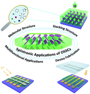
Organic semiconductor single crystals (OSSCs) possess high mobility and ultra-long spin relaxation times in the millisecond or even second range, mainly due to their pure material systems, perfect periodic structures, and inherent weak spin–orbit coupling (SOC). Coupling this with their excellent photoelectric functionality, they have long been considered as perfect materials for organic spintronic applications to obtain both long-distance spin transport and novel multifunctionality at room temperature, attracting wide interest. Currently, spintronic studies based on OSSCs are still at the heuristic stage, and there are many related critical challenges, as well as important opportunities. Herein, this perspective article, relying on developed theory and in-depth investigations of organic semiconductors (OSCs) in electronics and spintronics, provides discussion and future prospects, focusing on several aspects of OSSCs; we aim to inspire progress in this new field and attempt to guide a wide range of research in related fields. Firstly, as the spin relaxation time and charge carrier mobility are the two main factors affecting the spin diffusion length, the effects of the molecular structure and stacking structure regarding these two factors are discussed, covering material design and regulation methods in detail. Then, the current situation and challenges relating to device fabrication technology based on OSSCs are outlined, highlighting what needs to be solved in order to build a foundation for achieving extra-long spin transport in OSSCs and novel multifunctional OSSC-based spintronic devices. Finally, based on various reported multifunctional spintronic devices and OSSCs with excellent photoelectric properties, the exploitation of novel multifunctional spintronic devices is discussed.


image file: d1tc04333a-p1.tif

Mingyi Ding

Mingyi Ding grew up in Shandong Province, P. R. China. She received her BS degree in 2018 from Southwest Minzu University. She is currently a graduate student jointly trained by the School of Science of Tianjin University and National Center for Nanoscience and Technology. Her current research interests include spin transport in organic semiconductors.

image file: d1tc04333a-p2.tif

Rui Zhang

Dr. Rui Zhang received his PhD from University of Science and Technology of China (USTC) in 2017. Dr. Zhang is currently a postdoctoral research fellow at National Center for Nanoscience and Technology (NCNST), China. His research interests mainly focus on the rational design and controllable synthesis of nanomaterial electrocatalysts for electrocatalytic applications.

image file: d1tc04333a-p3.tif

Rongjin Li

Rongjin Li received his PhD from Institute of Chemistry, Chinese Academy of Sciences in 2009 under Prof. Wenping Hu's supervision. From 2009–2011, he was a postdoc in Prof. Hongxiang Li's group at Shanghai Institute of Organic Chemistry, Chinese Academy of Sciences. From 2011 to 2015, he worked in Prof. Klaus Müllen's group at Max-Planck-Institute for Polymer Research. Then he joined Tianjin University as a full Professor. His research focuses on 2D molecular crystals and optoelectronic devices. He is an academic editor of SmartMat.

image file: d1tc04333a-p4.tif

Xiaotao Zhang

Xiaotao Zhang is an associate Professor at Tianjin University. He was born in 1982 in Henan Province, China. He received his PhD degree from the Institute of Chemistry, Chinese Academy of Sciences in 2012 after obtaining his MSc degree (2007) from Zhejiang University. His research work includes the design and synthesis of novel organic semiconductors and the fabrication and characterization of organic optoelectronic devices.

image file: d1tc04333a-p5.tif

Xiangnan Sun

Xiangnan Sun has been a professor and group leader at NCNST since 2016. He graduated with a BS degree in 2003 and MS degree in 2006 from Qingdao University of Science and Technology. He obtained his PhD in 2011 from the Institute of Chemistry, CAS. From 2012 to 2015, he worked as postdoctoral researcher in the Nanodevice Department at CIC nanoGUNE located in Spain. His current research interests include organic semiconductors and their electrical and spintronic applications.


1. Introduction

π-conjugated organic semiconductors (OSCs) composed of light elements1 offer weak spin–orbit coupling (SOC) strength and thus, long spin relaxation times in the millisecond or even second range in theory,2 making OSCs attractive and promising in the field of spintronics.3 Since the advent of organic spintronics,4,5 room-temperature long-distance spin transport has been a long-term goal for OSCs.6 In particular, with the development of multifunctional organic spintronic devices7 and further explorations of spin manipulation,8 the pursuit of high-efficiency spin transport gained increasing focus. The spin diffusion length λs, a parameter used to assess the spin transport ability of an OSC, can be described as follows:
 
image file: d1tc04333a-t1.tif(1)
where D is the charge carrier diffusion constant, which is expressed as follows:
 
D = kBT μ/e,(2)
and τs is the spin relaxation time. Due to the relationship between D and the carrier mobility μ, in which kB is the Boltzmann constant, T is the temperature, and e is the elementary charge, the spin transport properties of OSCs are highly dependent on the charge carrier mobility and spin relaxation time.9 Unfortunately, impurities and defect states commonly existing in polycrystalline and amorphous OSC thin films, such as multi-grain boundaries, disordered molecular stacking, unclean interfaces, etc., can easily result in the strong scattering of spin-polarized carriers, thus hindering spin transport in OSCs.10

In order to overcome the above-mentioned intrinsic defects in most OSCs, OSSCs with pure material systems and long-range-order structures are considered as ideal spin transport candidates.10 Particularly, the unique band-like charge transport mode in OSSCs generally leads to high carrier mobility, which can reach 10 cm2 V−1 s−1.11–20 As a result, combining the high carrier mobility of an OSSC and its ultra-long spin relaxation time, a micrometre-level spin diffusion length can be estimated, demonstrating the great potential for achieving super-long spin transport distances in OSSC-based spintronic devices.21 However, it is worth noting that the construction of spintronic devices based on OSSCs still faces huge challenges10 and characterization of spin-related performance and the development of device functionality are still difficult to carry out, which has greatly restricted progress relating to organic single-crystal spintronics. Consequently, due to excellent advancements in the area of organic electronics22–24 and the growing requirement for organic spintronics,6,7 OSSCs are highly expected to be used in in-depth studies of organic spintronics and to help in achieving high-efficiency spin transport and further multifunctional applications.

This perspective article aims to offer theoretical and experimental guidelines for achieving the above goals. Firstly, the combination of two main factors, spin relaxation time and carrier mobility, initiates a series of discussions about how molecular chemical structure and stacking structure can affect the spin diffusion length, in order to provide a reference when selecting appropriate single-crystal spintronic materials. Subsequently, the current situation and challenges relating to device fabrication technology based on OSSCs are outlined, aiming to support the creation of universal device-construction methods to obtain high-efficiency spin transport in OSSCs. In addition, relying on a host of developed theoretical and experimental results from organic electronics, the exploitation of single-crystal multifunctional spintronic devices is discussed.

2. OSSC molecule design for long spin relaxation times

In theory, long-distance spin transport should be commonly found in OSCs due to the existence of weak SOC.1,2 Currently, despite this, there are relatively few OSCs that can actually achieve long-distance spin transport (greater than 100 nm) at room temperature.6 Therefore, exploring appropriate OSCs with high-efficiency spin transport abilities is urgent in the field of spintronics. From eqn (1) (shown above), it can be inferred that the spin relaxation time is a vital contributing factor when optimizing the spin transport distance in organic spintronics. The circumvention of the heavy atom effect25 and an understanding of the isotope effect26 are of equal importance when designing appropriate spin-transport materials, for reasons of ensuring weaker SOC and hyperfine interactions (HFIs) to obtain longer spin lifetimes. It is also certain that the number of scattering centres of spin-polarized charge carriers during transport, such as impurities and traps in the matrix, should be reduced as far as possible.27,28

To conclude, designing rational molecular structures, especially OSSCs, to optimize spin relaxation times is of great importance and of far-reaching significance for guiding the development of spintronic devices to obtain ultra-long spin transport distances. From the perspective of theoretical research, OSSCs possess unique charge transport modes; therefore, the spin relaxation mechanisms of electrons in these π-conjugated structures is a fresh field worthy of further study.21 From the perspective of experimental research, only by exploring the spin relaxation mechanisms of organic materials can we control the factors affecting spin relaxation more effectively, thus ensuring longer spin lifetimes and spin transport distances during the process of electron transport. Spin relaxation in OSCs can be induced by SOC,25 HFIs,26 and various traps27,28 during spin transport.

2.1 Factors which influence the spin–orbit coupling

SOC, as an important source of spin relaxation, is coupling between the spin and charge angular momentum.25 In basic spintronic devices, spin electrons are easily relaxed due to the presence of strong SOC during the process of transport, thus reducing the spin relaxation time and spin transport distance.29 Therefore, weak SOC effects in OSCs are more beneficial for long-distance spin transport. Next, we will discuss how SOC effects affect the spin transport distances in organic single-crystal materials from the perspective of the spin relaxation time.
2.1.1 Elementary composition. In the first place, it is theoretically accepted that the SOC strength is proportional to the fourth power of the atomic number (Z4);1 this means that OSCs consisting of heavier atoms will possess stronger SOC, which might cause faster spin relaxation. As an example, in the tris(8-hydroxyquinolinato)X (Xq3) series, Alq3, Gaq3, Inq3 and Biq3, the influence of the heavy atom on the SOC gradually increases upon replacing the central element with a heavier one, since the surrounding electric field of a heavier atom is stronger and possesses anisotropy.30 In addition, the bond lengths and bond angles in the molecular structure will change as the mass of the central atom increases, in other words, the vibration mode energy and number of particles will change, further increasing the strength of the SOC effect.30 In addition, there is another point to note. Even with π-conjugated structures only containing different elements such as oxygen atoms (O), sulphur atoms (S), and selenium atoms (Se), the SOC effect on these molecules still follows the heavy atom effect.30
2.1.2 Molecular structure. Besides the heavy atom effect, specialized molecular structures can also cause different SOC effects. For instance, the degree of curvature in a conjugated OSC structure is demonstrated to provide a new way to tune the SOC strength, as observed for fullerene-based materials.31 Liang et al. confirmed that the spin relaxation of C70 molecules is weaker than that of C60 molecules via a comprehensive consideration of the thickness-dependence of the magnetoresistance (MR) based on the modified Jullière equation.32 This difference in SOC strength is mainly attributed to the greater curvature of C60 molecules than C70 molecules.

Also, using targeted alkylation in π-conjugated structures is a method for tuning the SOC strength.25 Based on current reports, the addition of an alkyl chain to a π-conjugated structure exerts a positive influence on the spin relaxation time due to a qualitative effect.25 Such an effect can weaken the SOC strength via reducing the spin density of the π-conjugated OSC, having the purpose of optimizing the spin relaxation time.25 And, more remarkably, a longer alkyl chain and less bending will have a favourable influence on weakening the strength of SOC.25 Additionally, there are two other considerations to be taken into account when introducing alkyl chains into π-conjugated structures, not affecting the qualitative effect of alkyl chains on the SOC strength. Relying on relatively mature design principles relating to the use of OSCs in electronics, firstly, the introduction of alkyl chains into π-conjugated structures can sometimes promote the solubility of organic materials;33,34 secondly, alkyl chains of suitable length may also make up for defects on a Si/SiO2 substrate, achieving the purpose of improving the performances of devices.35 These points can be used for reference for determining the length and structure of the alkyl chains used when designing OSSCs.

2.2 Factors which influence the hyperfine interactions

Another important source of spin relaxation is HFIs, which arise from coupling between the localized electron spin and the nuclear spin, and mainly originate from the half-integer nuclear spin of an atom.36,37 HFIs commonly cause spin decoherence and thus reduce the spin relaxation time.36,37 Thus, suppressing HFIs is also essential for designing organic materials with long spin relaxation times at room temperature. We will discuss effective methods to weaken the HFI effect in order to design organic single-crystal materials with long-distance spin transport.

The abundant carbon (12C) and hydrogen (1H) atoms in most OSCs possess half-integer nuclear spin, which is the main source of the HFI effect. Therefore, HFI-dominated spin relaxation mechanism has been thoroughly explored by means of the isotope effect, normally based on 12C and 1H.26,38 Deuteration (D) is normally employed to replace H in molecules, therefore changing the nuclear spin and magnetogyric ratio, as well as the effects of HFIs. For instance, in the polymer poly(dioctyloxy)phenylenevinylene (DOO-PPV), the H atoms on the main backbone were replaced by D atoms, with an unchanged molecular structure and chemical properties; due to the fact that the HFIs of D atoms are far weaker than H atoms, a longer spin relaxation time and remarkable MR are obtained in the device.26 Another common example is substitution between 12C and 13C. Along with an extension of the conjugation length and a reduction of the reorganization energy, the isotope effects of C atoms weaken the HFI strength in OSCs.39 This is because the stretching vibrations of aromatic carbon make a significant contribution to the reorganization energy.39 Aside from deuterium and 13C isotopes, other isotopes, such as 19F and 27Al, have been employed to study isotope effects through theoretical calculations,37 but there have been no practical examples of their use as organic spacers in device preparation, and further research is needed. Despite the isotope effect having confirmed the existence of HFIs based on theoretical calculation, experimental evidence still needs to be collected to better prove their importance.

So far, we still know little about the relationship between molecular structure and spin relaxation, and more effort must be devoted to this issue to obtain a clearer picture. As mentioned above, most current work on improving spin relaxation times is focused on the molecular level, including elementary compositions and chemical structures. Additionally, in molecular spintronics, studies of stacking structures have demonstrated an important impact on the electron transport process and, thus, on carrier mobility.22–24 Unfortunately, the relationship between the stacking structure and spin transport or diffusion is completely unknown, mainly because of limited fabrication techniques for OSSC-based spintronic devices. Next, we will discuss the influence of molecular stacking structures on spin transport performance and the potential for effectively regulating the stacking structure to obtain long-distance spin transport in OSSCs.

3. Stacking regulation for high mobility

According to eqn (1) and (2) (see above), high mobility is another important parameter for obtaining long-distance spin transport. Based on current progress relating to organic spintronics, most OSCs employed as organic spacers are in amorphous or poly-crystalline form in spintronic devices.6 These thin-film materials have disordered structures or multiple grain boundaries, obstructing charge carrier transport.10 Conversely, OSSCs with regular stacking arrangements can reduce charge scattering during the transport process, which is beneficial for obtaining high mobility.10 Different stacking arrangements in OSSCs will lead to different carrier mobilities and influence the spin diffusion length.

As far as OSSCs are concerned, four common stacking motifs are presented in Fig. 1: (i) the herringbone stacking motif with face-to-face π–π overlap, providing only one large transfer integral (Fig. 1a); (ii) the herringbone stacking motif without face-to-face π–π overlap, possessing three large transfer integrals, where edge-to-face π–π overlap is responsible for effective charge transport (Fig. 1b); (iii) the brick-wall stacking motif with two-dimensional (2D) π–π overlap, offering two large transfer integrals (Fig. 1c); and (iv) slipped-stack stacking with one-dimensional (1D) π–π overlap, resulting in one large transfer integral and charge transport only along the direction with π–π overlap (Fig. 1d).40 As can be seen from the stacking motifs, increasing the transfer integral and lowering the reorganization energy will promote the enhancement of the charge transfer rate, which in turn creates higher carrier mobility.41


image file: d1tc04333a-f1.tif
Fig. 1 Common molecular stacking motifs in organic semiconductor crystals:40 (a) the herringbone stacking motif with face-to-face π–π overlap; (b) the herringbone stacking motif with edge-to-face π–π overlap; (c) the brick-wall stacking motif with two dimensional π–π overlap; and (d) slipped-stack stacking with one dimensional π–π overlap.

From the four common stacking motifs, it can be perceived that OSSCs have structural anisotropy and, thus, the charge transport properties are distinct along different directions, in other words, generating mobility anisotropy.22,23 The level of mobility anisotropy is largely determined by the compactness of π–π stacking along the three crystalline axes.22,23 Therefore, the stacking motifs of OSSCs are an important factor for designing OSSC-based spintronic devices with different structures. Excellent progress has been made in the field of organic electronics,22–24 and of these four kinds of stacking motif, the herringbone stacking motif is the most common OSSC stacking motif for achieving high mobility.11 Additionally, the most ideal charge-transport paths in organic electronics arise from brick-wall packing with a 2D charge-transport network, in which interactions between adjacent molecules boost the π–π overlap.40 In theory,42,43 if an OSSC with a neat stacking structure has an “edge-on” arrangement on a substrate,43 it may be more suitable for constructing a spintronic device with a horizontal structure; if an OSSC with a neat stacking structure possesses a “face-on” arrangement on the substrate,44–46 it may be more beneficial for constructing a spintronic device with a vertical structure. It should be noted that both the four stacking motifs and “face-on” and “edge-on” orientation are used to describe the stacking structures of molecules in space. The former is classified in terms of the intermolecular arrangement and is commonly used for OSSCs. In contrast, the latter is classified based on the arrangement of molecules relative to the substrate and is commonly used for organic polycrystalline materials.

Since π–π stacking arrangements are strongly associated with high mobility and thus they affect the spin diffusion length in organic single-crystal layers, finding methods for regulating stacking arrangements is crucial when constructing high-efficiency spintronic devices based on OSSCs. Firstly, the modification of molecular structures is a usual method to adjust the molecular stacking arrangement. For example, the introduction of alkyl chains into dinaphtho[2,3-d:2′,3′-d′]benzo[1,2-b:4,5-b′] dithiophene (DNBDT) can change the compactness of π–π overlap because of van der Waals interactions between the alkyl chains; thus, the stacking structure is transformed into a mode that is beneficial for charge transport.47 In addition, the molecular structure of an OSSC with multiple bent conjugated π-cores can inhibit disordered aggregation, which is more conducive for achieving high mobility.47 Secondly, adopting different organic single-crystal growth techniques can also be used to adjust stacking arrangements. Based on studies of organic electronics, OSSCs grown via solution methods tend to have “edge-on” molecular orientation,43 which is beneficial for the construction of spintronic devices with horizontal structures, while OSSCs grown via vapor phase methods are suitable for spintronic devices with vertical structures because of the “face-on” molecular orientation.44–46 Thirdly, solvent effects may also be a potential way to regulate stacking motifs.48

Although studies of spin transport based on OSSCs with controllable stacking motifs have not been reported in the field of organic spintronics, studies of the effects of stacking structures on carrier mobility in organic electronics have laid solid foundations for the achievement of long-distance spin transport.22–24 Also, some information or reference points regarding the relationship between stacking structure and spin transport can be borrowed from inorganic counterparts. As reported in inorganic single crystals, since the magnetoelectric and electrical properties depend on different crystallographic planes, the resistance values of inorganic single crystals with different crystal planes are different.49,50 Thus, the relationship between the stacking structure of an OSSC and spin transport may also be discussed based on different crystal axes or crystallographic planes. It is also worth mentioning the fact that since there are obvious structural differences between inorganic and organic single-crystal materials,22,23,49–51 the methods used to characterize the resistivity of different crystallographic planes of inorganic crystals are not necessarily suitable for OSSCs, and further exploration is needed. However, the construction of spintronic devices based on OSSCs is still a great challenge because of a lack of feasible fabrication techniques. Therefore, to achieve high-efficiency spin transport in OSSCs, more effort needs to be devoted not only to exploring materials with suitable molecular structures and aggregation structures, but also to developing suitable methods for building reliable OSC-based spintronic devices.

4. Fabrication techniques for spintronic devices based on OSSCs

An organic spin valve (OSV) is the most typical spintronic device, which is made of one organic layer sandwiched vertically in between two ferromagnetic (FM) electrodes.1,52 The evaluation of the spin transport properties of conventional OSCs is normally carried out using this device.5,26,31,53,54 However, it is difficult to employ OSSCs in such a simple spintronic device. This is mainly because the weak van der Waals forces between organic molecules in an OSSC22 mean it shows poor thermal resistance, and it is easily damaged by the thermal energy and kinetic energy of metal atoms during the fabrication of the OSV.55,56 At present, the FM materials are normally deposited via thermal evaporation,57–60 e-beam evaporation,53,54,61–64 and magnetron sputtering,5,26,31,57–60 all of which possess very high thermal and kinetic energy. These high-energy preparation methods can cause the deconstruction and sublimation of the OSSC, as shown in Fig. 2. Therefore, none of the existing techniques for preparing molecular spin valves (MSVs)65 can be applied to fabricate OSSC-based SVs, and new approaches that can pattern top FM electrodes onto molecules using low or no thermal and kinetic energy need to be developed in the future.
image file: d1tc04333a-f2.tif
Fig. 2 A schematic diagram of a vertical spin valve device based on an OSSC, which shows the great challenges related to device fabrication. These include the sublimation and deconstruction of the OSSC because of high heat and kinetic energy during the deposition of the top electrode, and the adsorption of O2, H2O, and impurities at the surface of the bottom electrode, which will destroy efficient spin injection at the bottom interface.

Conversely, over ten years ago, OSSCs were introduced in the field of organic electronics, and fabrication techniques for electronic devices based on OSSCs are relatively more mature as a result of long-term development.22–24 Presently, one of the most common methods for device fabrication without damaging the properties of OSSCs is the “gold-layer sticking” technique, which involves transferring the metal film onto the single-crystal surface using a mechanical probe.55 Such an innovative fabrication method not only effectively suppresses damage to the single-crystal surface, but it can also prevent high leakage currents caused by metal penetration. Simultaneously, several similar device fabrication methods are also popular in organic electronics, such as the “organic ribbon mask” technique,56 “multiple-cycle gold wire mask moving” technique,66 and so on. In light of these excellent fabrication methods for organic single-crystal electronic devices,22,23 the development of construction methods for OSSC-based spintronic devices could benefit a lot by learning from this advantageous research.

Methods involving the mechanical transfer of top electrodes for organic spintronics should be taken into consideration when preparing OSSC-based SVs. For example, Ding et al. reported a non-damaging device fabrication method in which prefabricated electrodes are transferred to the organic layer via laminating technology.58 The use of such a nondestructive transfer strategy makes a significant contribution to optimizing the interface between the top ferromagnetic electrode and the OSSC. However, it is worth noting that effective contact between the ferromagnetic electrode and the OSSC must be maintained in this method. This contact determines whether the spin carrier can achieve effective spin injection, which is a prerequisite for obtaining long-distance spin transport at room temperature. In addition, the interface between the bottom electrode and the OSSC also needs attention, as shown in Fig. 2. Most bottom electrodes are exposed to air during the fabrication of OSSC-based spintronic devices, which can result in the adsorption of water, oxygen, and impurities on the surface of the bottom electrode.65 As is well-known, the presence of water and oxygen can seriously affect the performance of a multilayer device, especially an organic spintronic device.65 Some impurities from air attached to the surface of the bottom electrode can be regarded as an invalid layer in an organic spintronic device, inducing spin scattering and further increasing the resistance of the spintronic device. Moreover, the magnetic properties of FM electrodes should be kept constant during the transfer process. In reality, the preparation conditions mentioned above are very difficult to realize. It should also be noted that, upon examining current research progress, multifunctional spintronic devices, such as molecular spin photovoltaic devices, spin organic light-emitting diodes (spin-OLEDs), etc., have all been prepared based on organic spin valves. Therefore, the fabrication methods of these devices are interconnected, and metal penetration at the top electrode and the adsorption of impurities between the bottom electrode and the OSSC are universal problems faced during the fabrication of functional spintronic devices besides OSVs.

In addition to problems related to electrode fabrication, the large-area scale and homogeneous morphology of the OSSC are of equal importance during the construction of spintronic devices.23 This is due to the fact that the presence of such excellent morphological characteristics can effectively prevent leakage current. Synchronously, the thickness of the OSSC should be controlled during layer-by-layer growth22 to prevent high contact resistance owing to inhibited spin transport at the boundaries between layers. Briefly speaking, it is extremely difficult to successfully construct stable and reliable spintronic devices based on OSSCs at room temperature, let alone multifunctional spintronic devices based on OSSCs. However, relying on the excellent achievements mentioned above, OSSC-based spintronic devices are expected to be successfully constructed via nondestructive top electrode transfer and suitable OSSC growth methods in the future, which will promote the development of OSSC-based multifunctional spintronic devices.

5. The prospect of multifunctional spintronic devices based on OSSCs

Aside from having excellent transport properties, OSSCs with excellent photoelectric properties are also expected to be used to construct room-temperature multifunctional spintronic devices. In contrast to charge transport, the environmental demands in the organic layer are so high for the transport of spin-polarized electrons that impurities and defect states are not allowed;10 OSSCs are good materials, providing a very pure transport environment in spintronic devices. Also, their definite structures are beneficial for gaining an in-depth understanding of the structureproperty relationships and exploring spin-related physical phenomenon in comparison with ordinary polycrystalline OSCs.22–24 The development of multifunctional electronic devices based on OSSCs in the electronic area is relatively mature,22–24 covering devices such as organic light-emitting diodes (OLEDs),67,68 organic light-emitting transistors (OLETs),24,69 organic photovoltaic (OPV) devices,24,70 and so forth. Taking information from the abundant theoretical systems relating to organic electronics, versatile spintronic devices based on organic thin films are emerging in an endless stream.

A spin-OLED is a representative organic multifunctional spintronic device with hole injection and electronic transmission capabilities in which the current and electroluminescence are both controlled by an external magnetic field.71 Nguyen et al. reported the first spin-OLED, but this device only works at low temperature.71 To overcome this limitation, we can try to find a breakthrough relating to organic single-crystal electronics. In a related report, Ding et al. successfully constructed a single-crystal OLED with a multi-doped structure using a double-doped method, obtaining ideal white light.68 Based on the strength of this excellent result, the use of co-doping methods in single-crystal systems is expected to be a feasible approach for constructing spin-OLEDs based on OSSCs.

Recently, a brand-new functional device was reported by Sun in which, using a photosensitive material as the organic spacer in an OSV device, four resistance states can be observed in the same device upon the adjustment of the light irradiation and the external magnetic field; this is known as a spin photoresponse device.53 This finding opens up intriguing prospects for multifunctional sensing applications at room temperature. However, a few unfavorable conditions prevent optimized performance using such a device, including the influence of defect states, the on/off ratio of the device, and so on. Using a two-dimensional (2D) OSSC as the transport medium might be promising alternatives to the use of an OSC in this device, owing to the mechanical flexibility, high transparency, and effective transport. Recently, based on an ultra-thin 2D OSSC, Wang et al. successfully constructed a high-performance organic phototransistor, manifesting an ultrahigh on/off ratio and high responsivity.72 The results of this study verify the existence of a photo-response effect based on a single-crystal OSC and contribute to ingenious ideas for future optoelectronic devices utilizing organic spintronics.

Upon introducing a photovoltaic effect into an organic spintronic device, the coupling of the magnetic and optical responses results in a spin photovoltaic device, as developed by Sun et al.61 Such a device can generate fully spin-polarized current via balancing external partial spin-polarized injection and photo-generated carriers, realizing the modulation of the output current and MR values. Despite a host of remarkable works having been reported, there are still some tough challenges to overcome related to such devices, such as enhancing the photovoltaic effect, dealing with organic solvent residue, and so forth. OSSCs greatly meet the requirements for optimizing the performances of spin photovoltaic devices. Recently, Xiao et al. fabricated an ultra-thin vertical organic crystalline p–n heterojunction.70 Such a heterojunction with a high-quality interface was applied in an OPV device, displaying an open-circuit voltage of up to 1.04 V.70 This study offers new ideas for innovations relating to organic spin photovoltaic devices.

Apart from these three devices, an OLET based on an OSSC is also a novel multifunctional optoelectronic device, integrating the light-emitting performance of organic light-emitting diodes with the switching performance of organic field-effect transistors to realize the self-regulation of the light-emitting device.69 In light of this fresh design concept, anthracene-derivative compounds are frequently used to study the characteristic of OLETs, since the anthracene core unit is regarded as a highly emissive source. Recently, Qin et al. constructed OLETs based on single-crystal 2,6-diphenylanthracene (DPA) and 2,6-di(2-naphthyl) anthracene (dNaAnt) (Fig. 3), realizing efficient and balanced bipolar injection and transport by means of asymmetric structure design and an interface control strategy.69 High mobility and light-emitting properties are achieved in the same device and this offers new insights into the construction of multifunctional spintronic devices. In addition, the construction of OSSC-based OLETs may also be a powerful tool to study the intrinsic exciton dynamics of semiconductors, laying the foundation for the development of spin light-emitting devices. The effective integration of OLETs and spintronic functionality is expected in future studies.


image file: d1tc04333a-f3.tif
Fig. 3 Three OSSC materials, DPA,69 dNaAnt,69 and C6-DPA,70 with excellent photoelectric properties are expected to be employed in the construction of OSSC-based novel multifunctional spintronic devices.

6. Conclusions

To summarize, we evaluate prospective spintronic applications based on OSSCs. OSSCs with excellent structural properties offer ultra-long spin relaxation times and high mobilities, which are expected to allow super-long spin transport distances. This will change the current situation in which spin transport in common OSCs is limited to hundreds of nanometers. It is certain that exploring suitable OSSC materials via designing suitable molecular structures and modulating the stacking structure is indispensable for the optimization of spin transport performance. Furthermore, OSSC-based spintronic devices, as ways of studying spin transport mechanisms, face great challenges and there is a strong need to innovate in terms of device fabrication technology. Based on achievements relating to high-efficiency spin transport in OSSCs and reliable fabrication methods for OSSC-based spintronic devices, promising multifunctional spintronic devices could be constructed, utilizing the excellent photoelectric properties of OSSCs. The application of OSSC materials to spintronics, benefiting from developed theory and advanced studies in the field of molecular electronics, will greatly promote the development of molecular spintronics in the future.

Author contributions

M. Ding wrote this article, R. Zhang drew all figures in this article, all corresponding authors supervised this article, and all authors participated in discussing this article.

Conflicts of interest

There are no conflicts to declare.

Acknowledgements

This work is supported financially by the Ministry of Science and Technology of the People's Republic of China (2017YFA0206600), the National Natural Science Foundation of China (Grant No. 52050171, 51973043, 51803040, 51822301, 22175047, 52103203, 52103338 and 91963126), the CAS Instrument Development Project (Grant No. YJKYYQ20170037), the Strategic Priority Research Program of the Chinese Academy of Sciences (Grant No. XDB36020000), Beijing National Laboratory for Molecular Sciences (Grant No. BNLMS201907), the CAS Pioneer Hundred Talents Program, The Natural Science Foundation of Shandong Province (Grant No. ZR2020ME070), and China Postdoctoral Science Foundation (Grant No. 2021M690802, 2018M630123).

Notes and references

  1. V. A. Dediu, L. E. Hueso, I. Bergenti and C. Taliani, Nat. Mater., 2009, 8, 707–716 CrossRef CAS.
  2. C. Boehme and J. M. Lupton, Nat. Nanotechnol., 2013, 8, 612–615 CrossRef CAS PubMed.
  3. D. Li and G. Yu, Adv. Funct. Mater., 2021, 31, 2100550 CrossRef CAS.
  4. V. Dediu, M. Murgia, F. C. Matacotta, C. Taliani and S. Barbanera, Solid State Commun., 2002, 122, 181–184 CrossRef CAS.
  5. Z. Xiong, D. Wu, Z. V. Vardeny and J. Shi, Nature, 2004, 427, 821–824 CrossRef CAS.
  6. L. Guo, Y. Qin, X. Gu, X. Zhu, Q. Zhou and X. Sun, Front. Chem., 2019, 7, 428 CrossRef CAS.
  7. L. Guo, X. Gu, X. Zhu and X. Sun, Adv. Mater., 2019, 31, 1805355 CrossRef CAS.
  8. M. Gobbi, L. Pietrobon, A. Atxabal, A. Bedoya-Pinto, X. Sun, F. Golmar, R. Llopis, F. Casanova and L. E. Hueso, Nat. Commun., 2014, 5, 4161 CrossRef CAS.
  9. P. A. Bobbert, W. Wagemans, F. W. A. van Oost, B. Koopmans and M. Wohlgenannt, Phys. Rev. Lett., 2009, 102, 156604 CrossRef CAS.
  10. H. Jang and C. A. Richter, Adv. Mater., 2017, 29, 1602739 CrossRef.
  11. D. Ji, T. Li, J. Liu, S. Amirjalayer, M. Zhong, Z.-Y. Zhang, X. Huang, Z. Wei, H. Dong, W. Hu and H. Fuchs, Nat. Commun., 2019, 10, 12 CrossRef CAS.
  12. Y. Krupskaya, M. Gibertini, N. Marzari and A. Morpurgo, Adv. Mater., 2015, 27, 2453–2458 CrossRef CAS PubMed.
  13. K. Takimiya, K. Bulgarevich, M. Abbas, S. Horiuchi, T. Ogaki, K. Kawabata and A. Ablat, Adv. Mater., 2021, 33, 2102914 CrossRef CAS.
  14. P. He, Z. Tu, G. Zhao, Y. Zhen, H. Geng, Y. Yi, Z. Wang, H. Zhang, C. Xu, J. Liu, X. Lu, X. Fu, Q. Zhao, X. Zhang, D. Ji, L. Jiang, H. Dong and W. Hu, Adv. Mater., 2015, 27, 825–830 CrossRef CAS PubMed.
  15. Z. Zhang, L. Jiang, C. Cheng, Y. Zhen, G. Zhao, H. Geng, Y. Yi, L. Li, H. Dong, Z. Shuai and W. Hu, Angew. Chem., Int. Ed., 2016, 55, 5206–5209 CrossRef CAS PubMed.
  16. Y. Yuan, G. Giri, A. L. Ayzner, A. P. Zoombelt, S. C. B. Mannsfeld, J. Chen, D. Nordlund, M. F. Toney, J. Huang and Z. Bao, Nat. Commun., 2014, 5, 3005 CrossRef PubMed.
  17. F. Qiu, Y. Dong, J. Liu, Y. N. Sun, H. Geng, Z. Hantang, D. Zhu, X. Shi, J. Liu, J. Zhang, S. Ai and L. Jiang, J. Mater. Chem. C, 2020, 8, 6006–6012 RSC.
  18. J.-H. Dou, Y.-Q. Zheng, Z.-F. Yao, T. Lei, X. Shen, X.-Y. Luo, Z.-A. Yu, S.-D. Zhang, G. Han, Z. Wang, Y. Yi, J.-Y. Wang and J. Pei, Adv. Mater., 2015, 27, 8051–8055 CrossRef CAS.
  19. H. Minemawari, T. Yamada, H. Matsui, J. Y. Tsutsumi, S. Haas, R. Chiba, R. Kumai and T. Hasegawa, Nature, 2011, 475, 364–367 CrossRef CAS PubMed.
  20. R. Zeis, C. Besnard, T. Siegrist, C. Schlockermann, X. L. Chi and C. Kloc, Chem. Mater., 2006, 18, 244–248 CrossRef CAS.
  21. J. Tsurumi, H. Matsui, T. Kubo, R. Hausermann, C. Mitsui, T. Okamoto, S. Watanabe and J. Takeya, Nat. Phys., 2017, 13, 994–998 Search PubMed.
  22. C. Wang, H. Dong, L. Jiang and W. Hu, Chem. Soc. Rev., 2018, 47, 422–500 RSC.
  23. Y. Wang, L. Sun, C. Wang, F. Yang, X. Ren, X. Zhang, H. Dong and W. Hu, Chem. Soc. Rev., 2019, 48, 1492–1530 RSC.
  24. X. Zhang, H. Dong and W. Hu, Adv. Mater., 2018, 30, 1801048 CrossRef PubMed.
  25. S. Schott, E. R. McNellis, C. B. Nielsen, H.-Y. Chen, S. Watanabe, H. Tanaka, I. McCulloch, K. Takimiya, J. Sinova and H. Sirringhaus, Nat. Commun., 2017, 8, 15200 CrossRef PubMed.
  26. T. D. Nguyen, G. Hukic-Markosian, F. Wang, L. Wojcik, X.-G. Li, E. Ehrenfreund and Z. V. Vardeny, Nat. Mater., 2010, 9, 345–352 CrossRef CAS PubMed.
  27. Z. G. Yu, Nat. Commun., 2014, 5, 4842 CrossRef CAS PubMed.
  28. I. Bergenti, F. Borgatti, M. Calbucci, A. Riminucci, R. Cecchini, P. Graziosi, D. A. MacLaren, A. Giglia, J. P. Rueff, D. Ceolin, L. Pasquali and V. Dediu, ACS Appl. Mater. Interfaces, 2018, 10, 8132–8140 CrossRef CAS.
  29. Z. G. Yu, Phys. Rev. Lett., 2011, 106, 106602 CrossRef CAS PubMed.
  30. L. Nuccio, M. Willis, L. Schulz, S. Fratini, F. Messina, M. D'Amico, F. L. Pratt, J. S. Lord, I. McKenzie, M. Loth, B. Purushothaman, J. Anthony, M. Heeney, R. M. Wilson, I. Hernandez, M. Cannas, K. Sedlak, T. Kreouzis, W. P. Gillin, C. Bernhard and A. J. Drew, Phys. Rev. Lett., 2013, 110, 216602 CrossRef CAS PubMed.
  31. X. Zhang, S. Mizukami, T. Kubota, Q. Ma, M. Oogane, H. Naganuma, Y. Ando and T. Miyazaki, Nat. Commun., 2013, 4, 1392 CrossRef.
  32. S. Liang, R. Geng, B. Yang, W. Zhao, R. C. Subedi, X. Li, X. Han and N. Tho Duc, Sci. Rep., 2016, 6, 19461 CrossRef CAS PubMed.
  33. C. Wang, H. Dong, W. Hu, Y. Liu and D. Zhu, Chem. Rev., 2012, 112, 2208–2267 CrossRef CAS.
  34. J. Chen and Y. Cao, Acc. Chem. Res., 2009, 42, 1709–1718 CrossRef CAS PubMed.
  35. P. Stoliar, R. Kshirsagar, M. Massi, P. Annibale, C. Albonetti, D. M. de Leeuw and F. Biscarini, J. Am. Chem. Soc., 2007, 129, 6477–6484 CrossRef CAS.
  36. P. A. Bobbert, Nat. Mater., 2010, 9, 288–290 CrossRef CAS.
  37. Z. G. Yu, F. Ding and H. Wang, Phys. Rev. B: Condens. Matter Mater. Phys., 2013, 87, 205446 CrossRef.
  38. T. D. Nguyen, B. R. Gautam, E. Ehrenfreund and Z. V. Vardeny, Phys. Rev. Lett., 2010, 105, 166804 CrossRef CAS.
  39. Y. Jiang, H. Geng, W. Li and Z. Shuai, J. Chem. Theory Comput., 2019, 15, 1477–1491 CrossRef CAS.
  40. S. Fratini, M. Nikolka, A. Salleo, G. Schweicher and H. Sirringhaus, Nat. Mater., 2020, 19, 491–502 CrossRef CAS.
  41. H. Dong, X. Fu, J. Liu, Z. Wang and W. Hu, Adv. Mater., 2013, 25, 6158–6182 CrossRef CAS PubMed.
  42. Y. Yao, H. Dong and W. Hu, Adv. Mater., 2016, 28, 4513–4523 CrossRef CAS.
  43. J. Yao, Y. Zhang, X. Tian, X. Zhang, H. Zhao, X. Zhang, J. Jie, X. Wang, R. Li and W. Hu, Angew. Chem., Int. Ed., 2019, 58, 16082–16086 CrossRef CAS PubMed.
  44. D. He, Y. Zhang, Q. Wu, R. Xu, H. Nan, J. Liu, J. Yao, Z. Wang, S. Yuan, Y. Li, Y. Shi, J. Wang, Z. Ni, L. He, F. Miao, F. Song, H. Xu, K. Watanabe, T. Taniguchi, J.-B. Xu and X. Wang, Nat. Commun., 2014, 5, 5162 CrossRef CAS PubMed.
  45. F. Yang, L. Jin, L. Sun, X. Ren, X. Duan, H. Cheng, Y. Xu, X. Zhang, Z. Lai, W. Chen, H. Dong and W. Hu, Adv. Mater., 2018, 30, 1801891 CrossRef.
  46. J. Liu, H. Zhang, H. Dong, L. Meng, L. Jiang, L. Jiang, Y. Wang, J. Yu, Y. Sun, W. Hu and A. J. Heeger, Nat. Commun., 2015, 6, 10032 CrossRef CAS.
  47. C. Mitsui, T. Okamoto, M. Yamagishi, J. Tsurumi, K. Yoshimoto, K. Nakahara, J. Soeda, Y. Hirose, H. Sato, A. Yamano, T. Uemura and J. Takeya, Adv. Mater., 2014, 26, 4546–4551 CrossRef CAS PubMed.
  48. J. H. Kim, S. K. Park, J. H. Kim, D. R. Whang, W. S. Yoon and S. Y. Park, Adv. Mater., 2016, 28, 6011–6015 CrossRef CAS PubMed.
  49. S. S. Aplesnin, L. I. Ryabinkina, G. M. Abramova, O. B. Romanova, N. I. Kiselev and A. F. Bovina, Phys. Solid State, 2004, 46, 2067–2072 CrossRef CAS.
  50. K. Eto, A. A. Taskin, K. Segawa and Y. Ando, Phys. Rev. B: Condens. Matter Mater. Phys., 2010, 81, 161202 CrossRef.
  51. M. El-Hagary, S. Soltan, M. Emam-Ismail and S. Althoyaib, J. Korean Phys. Soc., 2013, 62, 2093–2098 CrossRef CAS.
  52. D. Sun, E. Ehrenfreund and Z. V. Vardeny, Chem. Commun., 2014, 50, 1781–1793 RSC.
  53. X. Sun, A. Bedoya-Pinto, Z. Mao, M. Gobbi, W. Yan, Y. Guo, A. Atxabal, R. Llopis, G. Yu, Y. Liu, A. Chuvilin, F. Casanova and L. E. Hueso, Adv. Mater., 2016, 28, 2609–2615 CrossRef CAS.
  54. X. Sun, M. Gobbi, A. Bedoya-Pinto, O. Txoperena, F. Golmar, R. Llopis, A. Chuvilin, F. Casanova and L. E. Hueso, Nat. Commun., 2013, 4, 2794 CrossRef.
  55. Q. Tang, L. Jiang, Y. Tong, H. Li, Y. Liu, Z. Wang, W. Hu, Y. Liu and D. Zhu, Adv. Mater., 2008, 20, 2947–2951 CrossRef CAS.
  56. L. Jiang, J. Gao, E. Wang, H. Li, Z. Wang, W. Hu and L. Jiang, Adv. Mater., 2008, 20, 2735–2740 CrossRef CAS PubMed.
  57. Y. Wang, J. Yao, S. Ding, S. Guo, D. Cui, X. Wang, S. Yang, L. Zhang, X. Tian, D. Wu, C. Jin, R. Li and W. Hu, Sci. China Mater., 2021, 64, 2795–2804,  DOI:10.1007/s40843-021-1673-1.
  58. S. Ding, Y. Tian, H. Wang, Z. Zhou, W. Mi, Z. Ni, Y. Zou, H. Dong, H. Gao, D. Zhu and W. Hu, ACS Nano, 2018, 12, 12657–12664 CrossRef CAS.
  59. S. Ding, Y. Tian, H. Dong, D. Zhu and W. Hu, ACS Appl. Mater. Interfaces, 2019, 11, 11654–11659 CrossRef CAS PubMed.
  60. S. Ding, Y. Tian, Y. Li, W. Mi, H. Dong, X. Zhaner, W. Hu and D. Zhu, ACS Appl. Mater. Interfaces, 2017, 9, 15644–15651 CrossRef CAS.
  61. X. Sun, S. Velez, A. Atxabal, A. Bedoya-Pinto, S. Parui, X. Zhu, R. Llopis, F. Casanova and L. E. Hueso, Science, 2017, 357, 677–680 CrossRef CAS PubMed.
  62. K. Bairagi, D. G. Romero, F. Calavalle, S. Catalano, E. Zuccatti, R. Llopis, F. Casanova and L. E. Hueso, Adv. Mater., 2020, 32, 1906908 CrossRef CAS.
  63. S. Shi, Z. Sun, A. Bedoya-Pinto, P. Graziosi, X. Li, X. Liu, L. Hueso, V. A. Dediu, Y. Luo and M. Fahlman, Adv. Funct. Mater., 2014, 24, 4812–4821 CrossRef CAS.
  64. S. Shi, Z. Sun, X. Liu, A. Bedoya-Pinto, P. Graziosi, H. Yu, W. Li, G. Liu, L. Hueso, V. A. Dediu and M. Fahlman, Adv. Electron. Mater., 2018, 4, 1800077 CrossRef.
  65. S. Ding, Y. Tian and W. Hu, Nano Res., 2021, 14, 3653–3668,  DOI:10.1007/s12274-021-3310-6.
  66. Q. Tang, H. Li, Y. Song, W. Xu, W. Hu, L. Jiang, Y. Liu, X. Wang and D. Zhu, Adv. Mater., 2006, 18, 3010–3014 CrossRef CAS.
  67. R. Ding, M.-H. An, J. Feng and H.-B. Sun, Laser Photonics Rev., 2019, 13, 1900009 CrossRef CAS.
  68. R. Ding, F.-X. Dong, M.-H. An, X.-P. Wang, M.-R. Wang, X.-B. Li, J. Feng and H.-B. Sun, Adv. Funct. Mater., 2019, 29, 1807606 CrossRef.
  69. Z. Qin, H. Gao, J. Liu, K. Zhou, J. Li, Y. Dang, L. Huang, H. Deng, X. Zhang, H. Dong and W. Hu, Adv. Mater., 2019, 31, 1903175 CrossRef PubMed.
  70. M. Xiao, J. Liu, C. Liu, G. Han, Y. Shi, C. Li, X. Zhang, Y. Hu, Z. Liu, X. Gao, Z. Cai, J. Liu, Y. Yi, S. Wang, D. Wang, W. Hu, Y. Liu, H. Sirringhaus and L. Jiang, Nat. Commun., 2021, 12, 2774 CrossRef CAS.
  71. T. D. Nguyen, E. Ehrenfreund and Z. V. Vardeny, Science, 2012, 337, 204–209 CrossRef CAS.
  72. C. Wang, X. Ren, C. Xu, B. Fu, R. Wang, X. Zhang, R. Li, H. Li, H. Dong, Y. Zhen, S. Lei, L. Jiang and W. Hu, Adv. Mater., 2018, 30, 1706260 CrossRef.

This journal is © The Royal Society of Chemistry 2022