
Soft template-assisted self-assembly: a general strategy toward two-dimensional molecular crystals for high-performance organic field-effect transistors†‡
Xinzi
Tian§
a,
Jiarong
Yao§
a,
Siyu
Guo§
a,
Zhaofeng
Wang
a,
Yanling
Xiao
b,
Heng
Zhang
c,
Yiyu
Feng
 c,
Wei
Feng
c,
Jiansheng
Jie
b,
Fangxu
Yang
*a,
Rongjin
Li
*a and
Wenping
Hu
a
c,
Wei
Feng
c,
Jiansheng
Jie
b,
Fangxu
Yang
*a,
Rongjin
Li
*a and
Wenping
Hu
a
aTianjin Key Laboratory of Molecular Optoelectronic Sciences, Department of Chemistry, School of Science, Tianjin University & Collaborative Innovation Center of Chemical Science and Engineering, Tianjin 300072, China. E-mail: yangfangxu@tju.edu.cn; lirj@tju.edu.cn
bInstitute of Functional Nano & Soft Materials (FUNSOM), Jiangsu Key Laboratory for Carbon-Based Functional Materials & Devices, Soochow University, Suzhou 215123, China
cSchool of Materials Science and Engineering, Tianjin University, Tianjin 300072, China
First published on 16th December 2021
Abstract
Two-dimensional molecular crystals (2DMCs) are highly desirable to probe the intrinsic properties of organic semiconductors and are promising candidates for constructing high-performance optoelectronic devices. Liquids such as water are favorable substrates to produce high-quality 2DMCs because of the elimination of the ubiquitous coffee ring effect (CRE) of solid substrates. However, crystal growth on a water surface relies on solvents with high surface tension for good spreading, which severely limits the choice of solvents and thus the optimization of crystal growth. Herein, we reported a soft template-assisted self-assembly (STAS) strategy to grow large-area high-quality 2DMCs on a water surface irrespective of the surface tension of the solvents. The as-grown quasi-freestanding 2DMCs on the water surface could be transferred layer by layer to construct molecularly thin bilayer p–n heterojunctions. Organic field-effect transistors (OFETs) based on these p–n heterojunctions exhibited ambipolar charge transport characteristics with a hole mobility of up to 1.50 cm−2 V−1 s−1 and an electron mobility of up to 0.79 cm−2 V−1 s−1 under ambient air. The STAS strategy is applicable to solvents with both high and low surface tensions and organic semiconductors of various structures, and opens a new avenue for the construction of high-performance organic optoelectronic devices.
2D atomic crystals (e.g., graphene, transition metal dichalcogenides, and black phosphorus) have attracted significant attention for a variety of advanced optoelectronic applications due to their unique electronic and optical properties.1–6 As their counterparts, 2D molecular crystals (2DMCs) began to emerge as an increasingly important class of materials in recent years.7–11 2DMCs are thin layers of periodically arranged organic molecules held together by weak interactions (e.g., hydrogen bonds, van der Waals forces).12 2DMCs possess many intriguing advantages such as molecular-level thickness, atomically flat surface, low density of defects, functionality by design and solution processability, providing superior materials for both fundamental investigations and high performance optoelectronic devices.13–16
Up to now, several solution processing methods such as drop-coasting,10 bar-coating,17 and solution shearing18 have been proposed to grow 2DMCs on solid substrates. However, it is challenging to transfer as-grown 2DMCs to other substrates for device fabrication or to construct heterojunctions, which hinders their applications to a great extent. To solve this problem, several strategies to grow 2DMCs on liquid substrates (such as water) have been developed.19–21 Liquid substrates can eliminate the coffee ring effect (CRE) by depinning the three-phase contact line, which is favorable for the growth of large-area crystals. What's more, 2DMCs grown on liquid substrates can be transferred to any target substrates (e.g., Si, SiO2, quartz, and plastics) for devices or heterojunctions. For example, Xu et al. reported a solution epitaxy method to obtain 2DMCs on a water surface in which good spreading of the solvent was critical.21 Wang et al. obtained large-area 2DMCs by a space-confined self-assembly strategy, where the spreading area of the solution was increased by a phase transfer surfactant.20 It is worth noting that all the above methods used high surface tension solvents (γ > 28.5 mN m−1, e.g., chlorobenzene22 and xylene23) to maintain the unity of the solution on the water surface. The reason was that if a low surface tension solution (γ < 28.5 mN m−1, e.g., toluene,23 dichloromethane24 and trichloromethane24) was used, water with a high surface tension of 72 mN m−1 would separate the solution into many small liquid lenses, failing in producing high-quality 2DMCs. Relying on solvents with high surface tension severely limits the choice of solvents and thus the optimization of the crystal growth for high-quality 2DMCs.
Herein, a soft template-assisted self-assembly (STAS) strategy was developed to grow large-area high-quality 2DMCs on a water surface irrespective of the surface tension of the solvents. A surfactant, perfluorooctanesulfonic acid potassium (C8F17KO3S), was added into the water phase and it formed a molecular layer on the water surface, which worked as a soft template to support the organic solutions. As a result, solvents with both low and high surface tensions could spread continuously over a large area on the water surface without splitting, which was favorable for the production of ultrathin and large-area 2DMCs. In addition, the STAS strategy was proven to be applicable to a variety of organic semiconductors, including p-type semiconductors (e.g., 2,6-bis(4-hexylphenyl)anthracene (C6-DPA), 6,13-bis(triisopropylsilylethynyl)pentacene (TIPS-PEN), and 2,7-dioctyl[1]benzothieno[3,2-b][1]benzothiophene (C8-BTBT)) and a n-type semiconductor (a furan–thiophene quinoidal compound (TFT-CN)). What's more, the as-grown quasi-freestanding 2DMCs on the water surface could be transferred easily layer by layer to form bilayer p–n heterojunctions. Ambipolar organic field-effect transistors (aOFETs) based on the 2DMC p–n heterojunctions showed high hole mobility up to 1.50 cm−2 V−1 s−1 and high electron mobility up to 0.79 cm−2 V−1 s−1 under ambient air.
Toluene was selected as a solvent with low surface tension (γ = 28.5 mN m−1) and C6-DPA, a well-known high-performance soluble organic semiconductor, was chosen as an archetype material to demonstrate the STAS strategy. Fig. 1a–d showed the spreading of a toluene solution of C6-DPA on the water surface (see Fig. S1 and S2, ESI‡ for details), from which two conclusions can be drawn. (1) The total wetting area decreased as the concentration of the surfactant increased from 0 to 0.02 mg mL−1 (Fig. 1a–d). The reason was that the surface tension of water was reduced (Fig. S3, ESI‡), and thus the value of spreading coefficient was reduced, resulting in a reduced tendency of wetting and thus a reduced wetting area.20,25 (2) The extent of splitting of the wetting layer decreased as the concentration of the surfactant increased (Fig. 1a–d). Although the total wetting area was the largest on the pure water surface, the solution film was very thin and easily split into many small pieces possibly perturbed by the solvent vapor from evaporation (Fig. 1a). Many small and thick crystals formed on the pure water surface after solvent evaporation (Fig. 1e). As the concentration of the surfactant increased from 0 to 0.005 mg mL−1, although splitting still occurred, the tendency was largely reduced and discontinuous thin crystals formed on the water surface after solvent evaporation (Fig. 1b, c, f and g). When the concentration of the surfactant reached 0.02 mg mL−1, splitting was totally suppressed and a continuous thin wetting layer of solution was obtained on the water surface (Fig. 1d). When the solvent dried, large-area 2DMCs were obtained (Fig. 1h).
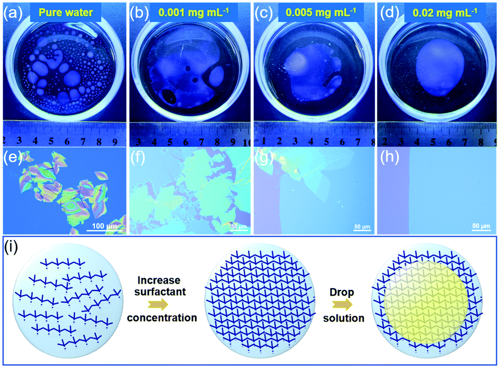 | ||
| Fig. 1 The spreading of a toluene solution of C6-DPA on water without the surfactant and with different concentrations of the surfactant. The concentrations of the surfactant were (a) 0, (b) 0.001 mg mL−1, (c) 0.005 mg mL−1 and (d) 0.02 mg mL−1. (e–h) Corresponding OM images of the C6-DPA 2DMCs grown on the water substrate. (i) Schematic diagram of the principle of the STAS strategy. | ||
Judging from the above observations, the mechanism was deduced to be a soft template-assisted self-assembly (Fig. 1i). The amphiphilic surfactant molecules spontaneously concentrated at the air/water interface, forming a soft molecular layer with their hydrophilic groups facing water and hydrophobic groups facing air.26,27 Such a soft molecular layer reduced the tendency of wetting by the reduction of the surface tension of water and thus the spreading coefficient. As a result, it helped to prevent the excessive spreading of a solution with low surface tension of the solvent, which was not conductive to the growth of large-area 2DMCs. Moreover, the soft molecular layers of the surfactant helped the continuous spreading of the thin solution layer on the water surface by acting as a supporting layer. A continuous and thin layer of the solution was critical for the growth of large-area 2DMCs.20 With the help of the dual role of the soft molecular layer of surfactants, the STAS strategy worked well with other low surface tension solvents such as trichloromethane and dichloromethane (Fig. S4, ESI‡). Meanwhile, taking advantage of the ability of continuous spreading of the solvents, the STAS strategy was applicable to high surface tension solvents (e.g., chlorobenzene and xylene, Fig. S5, ESI‡). In addition, both p- and n-type organic semiconductors can be prepared (Fig. S6–S9, ESI‡). By using the STAS strategy, solvents with both low and high surface tensions could spread continuously over a large area on the water surface without splitting to produce ultrathin and large-area 2DMCs.
Fig. 2a and e showed the typical optical microscopy (OM) images of C6-DPA and TFT-CN 2DMCs, respectively. The surfaces of both 2DMCs were smooth without any obvious cracks. Polarized optical microscopy (POM) images of C6-DPA and TFT-CN 2DMCs were shown in Fig. S8 and S9 (ESI‡), the colour of the films changed uniformly when the samples were rotated by 45°, confirming the single-crystalline nature of both 2DMCs. The thicknesses of C6-DPA and TFT-CN 2DMCs were measured by atomic force microscopy (AFM, Fig. 2b and f), and were 8.4 nm and 2.5 nm, respectively, corresponding to three and two molecular layers. The root mean square roughnesses of C6-DPA and TFT-CN 2DMCs were 0.13 nm and 0.24 nm, respectively, indicating their atomically flat surfaces (Fig. 2b and f). The X-ray diffraction (XRD) patterns of C6-DPA and TFT-CN 2DMCs were depicted in Fig. S10 and S11 (ESI‡), respectively. Sharp diffraction peaks at 2θ = 2.7°, 5.5° and 13.7° were observed in the XRD pattern of C6-DPA (Fig. S10, ESI‡). The first peak at 2θ = 2.7° corresponded to a d-spacing of 3.2 nm.12 The sharp diffraction peak of TFT-CN at 2θ = 5.6° corresponded to a d-spacing of 16.0 Å, which could be indexed as the (001) plane based on the single crystal data of TFT-CN (Fig. S11, ESI‡).28 The selected area electron diffraction (SAED) patterns of C6-DPA and TFT-CN 2DMCs exhibited clear and ordered diffraction spots (Fig. 2c and g). The lattice vectors of C6-DPA and TFT-CN were measured by high-resolution atomic force microscopy (HRAFM) to further assess the crystallinity of the two 2DMCs. Fig. 2d and h show the molecular packing of C6-DPA and TFT-CN 2DMCs, respectively. Lattice constants of a = 6.40 Å, b = 8.16 Å, and θ = 86.7° for C6-DPA and a = 10.52 Å, b = 11.69 Å, and θ = 63.0° for TFT-CN were obtained, which indicated the ordered molecular packing of the two 2DMCs.12,28 All the above results demonstrated the single-crystalline nature of the two 2DMCs.
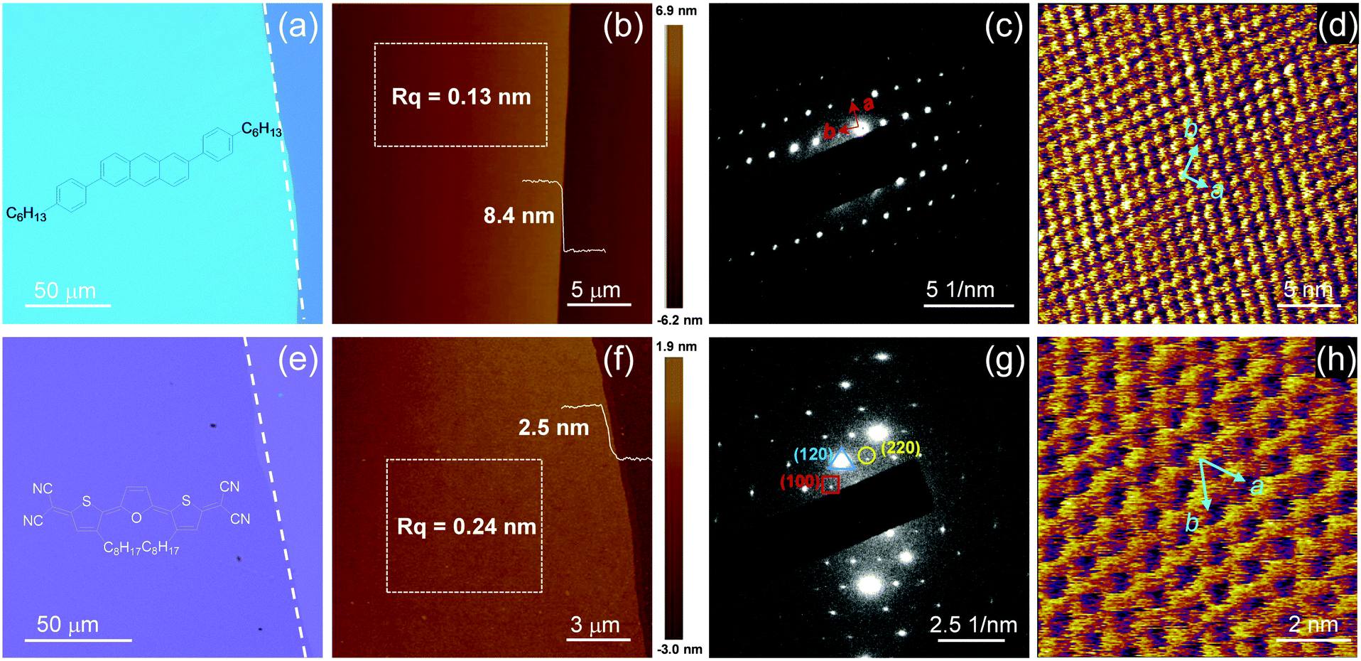 | ||
| Fig. 2 (a) OM image, (b) AFM image, (c) SAED pattern and (d) HRAFM image of a C6-DPA 2DMC. (e) OM image, (f) AFM image, (g) SAED pattern and (h) HRAFM image of a TFT-CN 2DMC. | ||
Encouraged by the high-quality of the single-crystalline 2DMCs, OFETs with top-contact bottom-gate configurations were constructed to investigate their electrical characteristics. Au (80 nm) was used as the source and drain electrodes by a stamping method,29 and octadecyltrichlorosilane (OTS)-modified SiO2/Si was used as the gate dielectric layer. Fig. 3a and d showed schematics of OFETs based on C6-DPA and TFT-CN 2DMCs, respectively. The charge transport properties of both C6-DPA and TFT-CN 2DMCs were examined under ambient air at room temperature. All devices exhibited typical transfer (Fig. 3b and e) and output curves (Fig. 3c and f), respectively. A hole mobility of 1.39 cm2 V−1 s−1 for C6-DPA and an electron mobility of 0.60 cm2 V−1 s−1 for TFT-CN were obtained, demonstrating the high performance of the as-grown 2DMCs.12,20,28
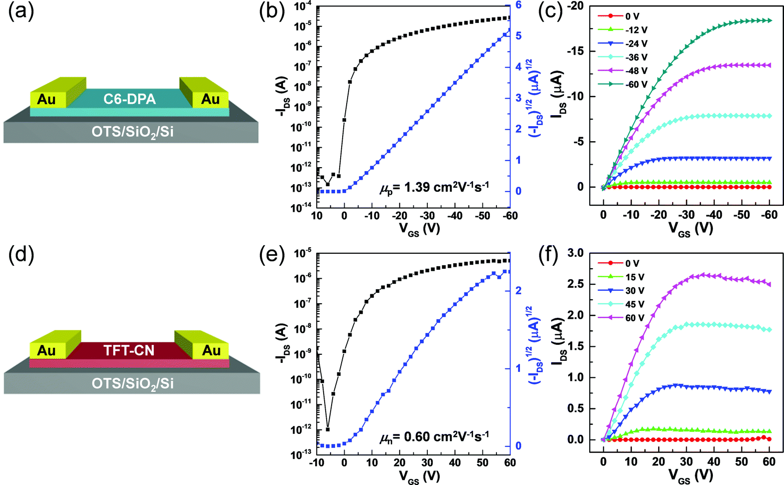 | ||
| Fig. 3 Schematics of OFETs based on (a) C6-DPA 2DMCs and (d) TFT-CN 2DMCs. (b) Transfer characteristics and (c) output characteristics of OFETs based on pristine C6-DPA 2DMCs. (e) Transfer characteristics and (f) output characteristics of OFETs based on pristine TFT-CN 2DMCs. | ||
The high performance of two pristine 2DMCs laid the foundation to construct bilayer p–n heterojunctions for high-performance aOFETs. Two pristine 2DMCs were grown on the water surface by the STAS strategy. Thereafter, C6-DPA and TFT-CN 2DMCs were sequentially stacked layer by layer to form bilayer p–n heterojunctions.30–32 Taking advantage of the layer-by-layer transfer method, bilayer heterojunctions composed of other 2DMCs could also be prepared (Fig. S12 and S13, ESI‡). OM and POM images of p–n heterojunctions based on C6-DPA and TFT-CN 2DMCs clearly showed the boundaries between the two pristine 2DMCs and the bilayer p–n heterojunctions (Fig. 4a–c). Under POM, the colour of the p–n heterojunctions changed uniformly when the samples were rotated by 45° (Fig. 4b and c), indicating the single-crystalline nature of the p–n heterojunctions. XRD patterns of the p–n heterojunctions exhibited sharp diffraction peaks of the characteristic peaks of both C6-DPA and TFT-CN, confirming the successful preparation of p–n heterojunctions and their high crystallinity (Fig. S14, ESI‡). The electrical properties of the bilayer p–n heterojunctions were investigated by constructing aOFETs with a top-contact bottom-gate configuration (the same as their OFETs based on pristine 2DMCs). All measurements were performed under ambient air at room temperature. Fig. 4d and g depicted the typical transfer characteristics of the aOFETs. V-Shape curves were seen in the transfer curves, which represented electron and hole transport, showing typical ambipolar transport characteristics. According to the double-channel model of aOFETs,33 holes and electrons were transported in different layers (Fig. S15, ESI‡). In the electron accumulation mode (VDS > 0, Fig. S15a in ESI‡), gate voltages (VGS) with a value greater than Vth,e (threshold voltage for electron accumulation, ≈ 4 V, Fig. 4d) induced electrons in the TFT-CN layer. Electrons were then transported in the TFT-CN layer driven by VDS. Similarly, in the hole accumulation mode (VDS < 0, Fig. S15b in ESI‡), a negative VGS with a value smaller than Vth,h (threshold voltage for hole accumulation, ≈ −10 V, Fig. 4g), induced holes, which were then transported in the C6-DPA layer driven by VDS. In n-channel operation mode, when low VGS and high VDS were applied, the output curves of aOFETs exhibited a significant increase in drain current (IDS) because of the transport of both electrons and holes (Fig. 4e). When a high VGS was applied, typical saturation characteristics of n-type devices were observed. Similar results were observed in the p-channel operation mode (Fig. 4h).34–36 Moreover, in the output curves of both p- and n-channels, the linear relationship between IDS and VDS at low VDS indicated small contact resistances between the electrodes and the semiconductors.29,37 Because of the high quality of the bilayer p–n heterojunctions composed of 2DMCs, the performance of the aOFETs was one of the highest values based on bilayer p–n heterojunctions (Table S1, ESI‡).29,31,37–43 The maximum mobility was up to 1.50 cm2 V−1 s−1 for holes and 0.79 cm2 V−1 s−1 for electrons. Fig. 4f and i showed histograms of the hole and electron mobilities based on bilayer p–n heterojunctions composed of 2DMCs among 15 devices. The average mobility reached up to 1.16 cm2 V−1 s−1 for holes and 0.59 cm−2 V−1 s−1 for electrons. These results demonstrated that high-quality 2DMCs provided superior materials to construct high-performance aOFETs.
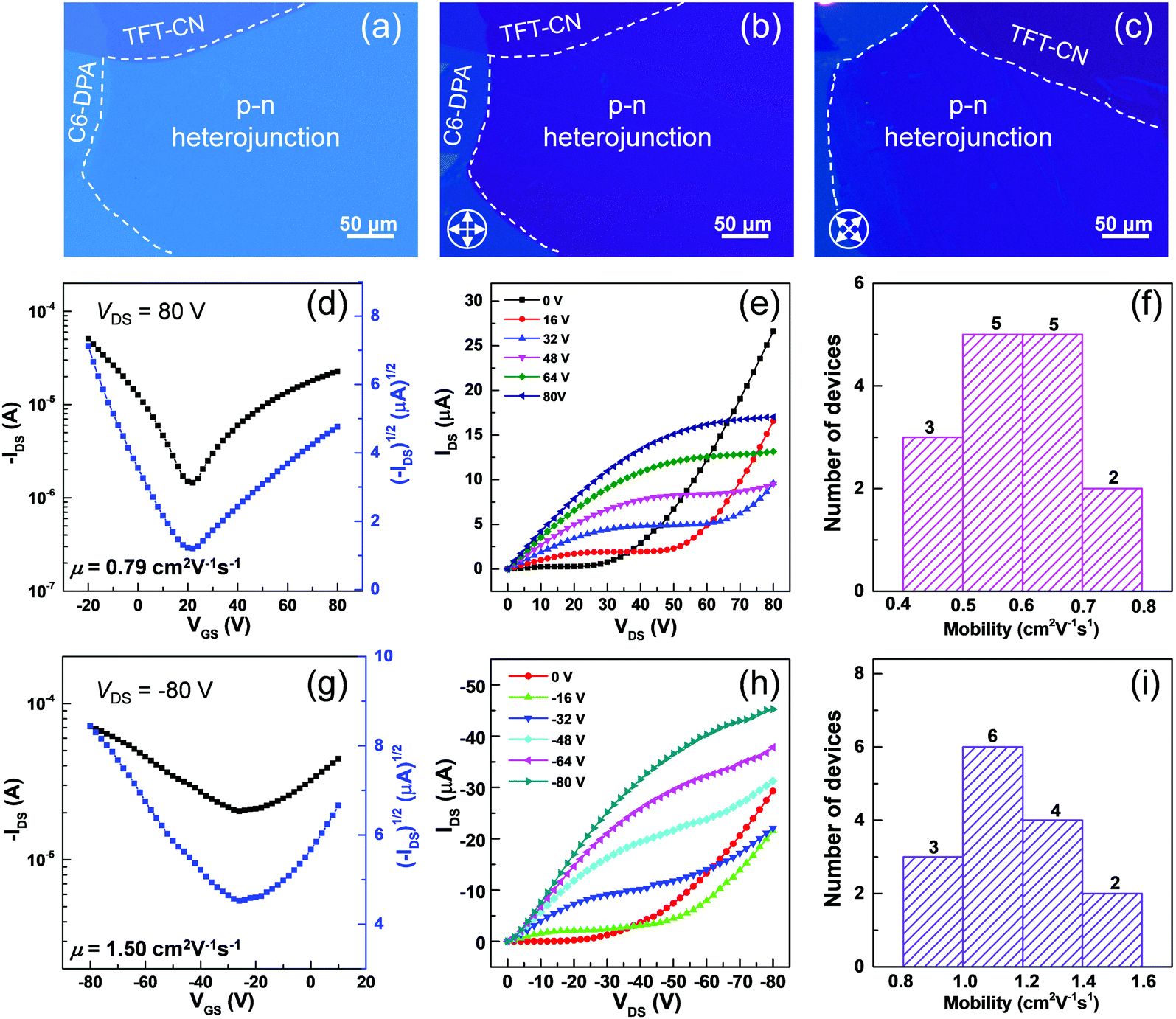 | ||
| Fig. 4 (a) OM and (b and c) POM images of the p–n heterojunctions. (d) Transfer characteristics, (e) output characteristics, and (f) the mobility distribution at VDS = 80 V. (g) Transfer characteristics, (h) output characteristics, and (i) the mobility distribution at VDS = −80 V. | ||
The high performance of aOFETs based on the bilayer p–n heterojunctions was ascribed to three main reasons. (i) The molecular thicknesses of pristine C6-DPA and TFT-CN 2DMCs effectively reduced the contact resistances and achieved high injection efficiency. (ii) The highly ordered single-crystalline nature of the pristine 2DMCs was beneficial to charge transport in aOFETs. (iii) The atomically flat surfaces of the pristine 2DMCs provide smooth interfaces of the bilayer p–n heterojunctions, which facilitate charge transport in double-channel aOFETs.
Conclusions
In summary, we developed a STAS strategy to prepare large-area high-quality 2DMCs on water surfaces irrespective of the surface tension of the solvents. In this method, a surfactant was used as a soft template to help the spreading of the solution at the air/water interface, which was favorable for the production of large-area 2DMCs. The STAS strategy was applicable to several organic semiconductors. High-performance aOFETs were constructed based on bilayer p–n heterojunctions composed of quasi-freestanding 2DMCs. High hole mobility of up to 1.50 cm−2 V−1 s−1 and electron mobility of up to 0.79 cm−2 V−1 s−1 under ambient air were obtained, respectively. The STAS strategy gets rid of the limitation of the solvents, and opens a new avenue for the construction of high-performance organic optoelectronic devices.Experimental
Materials
C6-DPA and TFT-CN were purchased from Luminescence Technology Corp. TIPS-PEN was purchased from TCI. C8F17KO3S was purchased from Shanghai Adamas. Both compounds were used without purification.Characterizations
OM and POM images were captured using a Nikon ECLIPSE Ci-POL polarized optical microscope. SAED measurements were taken with a Tecnai G2 F20 S-TWIN transmission electron microscope at 200 kV accelerating voltage. Two types of AFM were performed in this work. For regular AFM, the thicknesses of 2DMCs were characterized by tapping mode AFM using a Bruker Dimension Icon system. For HRAFM, the molecular arrangements of 2DMCs were measured by contact mode using an Asylum Cypher S (Oxford Instrument) system. Fluorescence microscopy images were performed using a Leica DM2700M optical microscope with a plug-in fluorescence unit. XRD was performed on a Rigaku Smartlab diffractometer with monochromatic Cu Kα (λ = 1.541 Å) radiation.Substrate treatment
Highly doped n-Si wafers (with a 300 nm thick SiO2 layer) were cleaned by sonication sequentially in deionized water, acetone, and 2-propanol for 10 min each, followed by cleaning with oxygen plasma at 80 W for about 10 min. The cleaned wafers were immediately modified with OTS by a vapor phase method. The OTS-modified substrates were cleaned by sonification in chloroform, n-hexane and isopropanol, successively.Device construction and characterizations
In this experiment, 2DMCs were transferred to OTS-modified SiO2 (300 nm)/Si substrates. Au (80 nm) stripes were stamped on the 2DMCs surfaces as drain and source electrodes, respectively. Transistor characteristics were recorded using a 4200-SCS system connected to a probe station under room temperature in air. The mobility of the OFETs was calculated according to the formula: IDS = (W/2L) µCi (VGS − Vth)2, where W is the channel width, L is the channel length, µ is the field-effect mobility, Ci is the specific capacitance (Ci = 10 nF cm−2), VGS is the gate voltage, IDS is the drain current, and Vth is the threshold voltage.Author contributions
X. Tian, J. Yao and S. Guo contributed equally to this work. R. Li, F. Yang and W. Hu conceived the idea and directed the project. X. Tian and J. Yao prepared the 2DMCs and fabricated OFETs and measured the electrical properties. S. Guo helped to grow some of the TIPS-PEN and TFT-CN 2DMCs. Z. Wang tested the surface tension. Y. Xiao and J. Jie helped in the HRAFM measurements. H. Zhang, Y. Feng, and W. Feng helped to test the SAED of 2DMCs. All the authors analysed the experimental results and contributed to the discussion.Conflicts of interest
There are no conflicts to declare.Acknowledgements
This study was supported by the National Natural Science Foundation of China (No. 51873148, 51903186, 52073206, and 51633006).References
- Z. Wang, R. Li, C. Su and K. P. Loh, SmartMat, 2020, 1, e1013 Search PubMed.
- A. Chaturvedi, B. Chen, K. Zhang, Q. He, G. H. Nam, L. You, Z. Lai, C. Tan, T. H. Tran, G. Liu, J. Zhou, Z. Liu, J. Wang, E. H. T. Teo and H. Zhang, SmartMat, 2020, 1, e1011 CrossRef.
- X. Wang, Y. Cui, T. Li, M. Lei, J. Li and Z. Wei, Adv. Opt. Mater., 2019, 7, 1801274 CrossRef.
- L. Wang, X. Xu, L. Zhang, R. Qiao, M. Wu, Z. Wang, S. Zhang, J. Liang, Z. Zhang, Z. Zhang, W. Chen, X. Xie, J. Zong, Y. Shan, Y. Guo, M. Willinger, H. Wu, Q. Li, W. Wang, P. Gao, S. Wu, Y. Zhang, Y. Jiang, D. Yu, E. Wang, X. Bai, Z.-J. Wang, F. Ding and K. Liu, Nature, 2019, 570, 91–95 CrossRef CAS PubMed.
- C. Xu, L. Wang, Z. Liu, L. Chen, J. Guo, N. Kang, X.-L. Ma, H.-M. Cheng and W. Ren, Nat. Mater., 2015, 14, 1135–1141 CrossRef CAS PubMed.
- V. C. Tung, M. J. Allen, Y. Yang and R. B. Kaner, Nat. Nanotechnol., 2009, 4, 25–29 CrossRef CAS PubMed.
- C. Wang, B. Fu, X. Zhang, R. Li, H. Dong and W. Hu, ACS Cent. Sci., 2020, 6, 636–652 CrossRef CAS PubMed.
- J. Qian, S. Jiang, S. Li, X. Wang, Y. Shi and Y. Li, Adv. Mater. Technol., 2019, 4, 1800182 CrossRef.
- F. Yang, S. Cheng, X. Zhang, X. Ren, R. Li, H. Dong and W. Hu, Adv. Mater., 2018, 30, 1702415 CrossRef PubMed.
- L. Jiang, H. Dong, Q. Meng, H. Li, M. He, Z. Wei, Y. He and W. Hu, Adv. Mater., 2011, 23, 2059–2063 CrossRef CAS PubMed.
- J. Yao, X. Tian, R. Li and W. Hu, Sci. Sin.: Chim., 2020, 51, 21–40 Search PubMed.
- J. Yao, Y. Zhang, X. Tian, X. Zhang, H. Zhao, X. Zhang, J. Jie, X. Wang, R. Li and W. Hu, Angew. Chem., Int. Ed., 2019, 58, 16082–16086 CrossRef CAS PubMed.
- Y. Wang, L. Sun, C. Wang, F. Yang, X. Ren, X. Zhang, H. Dong and W. Hu, Chem. Soc. Rev., 2019, 48, 1492–1530 RSC.
- Q. Wang, S. Jiang, J. Qian, L. Song, L. Zhang, Y. Zhang, Y. Zhang, Y. Wang, X. Wang, Y. Shi, Y. Zheng and Y. Li, Sci. Rep., 2017, 7, 7830 CrossRef PubMed.
- N. R. Champness, Nat. Chem., 2014, 6, 757–759 CrossRef CAS PubMed.
- D. He, Y. Zhang, Q. Wu, R. Xu, H. Nan, J. Liu, J. Yao, Z. Wang, S. Yuan, Y. Li, Y. Shi, J. Wang, Z. Ni, L. He, F. Miao, F. Song, H. Xu, K. Watanabe, T. Taniguchi, J.-B. Xu and X. Wang, Nat. Commun., 2014, 5, 5162 CrossRef CAS PubMed.
- B. Peng, S. Huang, Z. Zhou and P. K. L. Chan, Adv. Funct. Mater., 2017, 27, 1700999 CrossRef.
- Y. Diao, B. C. Tee, G. Giri, J. Xu, D. H. Kim, H. A. Becerril, R. M. Stoltenberg, T. H. Lee, G. Xue, S. C. Mannsfeld and Z. Bao, Nat. Mater., 2013, 12, 665–671 CrossRef CAS PubMed.
- Z. Chen, S. Duan, X. Zhang and W. Hu, Sci. China: Chem., 2021, 64, 1057–1062 CrossRef CAS.
- Q. Wang, F. Yang, Y. Zhang, M. Chen, X. Zhang, S. Lei, R. Li and W. Hu, J. Am. Chem. Soc., 2018, 140, 5339–5342 CrossRef CAS PubMed.
- C. Xu, P. He, J. Liu, A. Cui, H. Dong, Y. Zhen, W. Chen and W. Hu, Angew. Chem., Int. Ed., 2016, 55, 9519–9523 CrossRef CAS PubMed.
- J. Shen, Y. He, J. Wu, C. Gao, K. Keyshar, X. Zhang, Y. Yang, M. Ye, R. Vajtai, J. Lou and P. M. Ajayan, Nano Lett., 2015, 15, 5449–5454 CrossRef CAS PubMed.
- F. M. Fowkes, J. Phys. Chem., 1963, 67, 2538–2541 CrossRef CAS.
- A. K. Singh and J. K. Singh, Appl. Surf. Sci., 2017, 416, 639–648 CrossRef CAS.
- I. Langmuir, J. Chem. Phys., 1933, 1, 756–776 CrossRef CAS.
- K. Liu, H. Qi, R. Dong, R. Shivhare, M. Addicoat, T. Zhang, H. Sahabudeen, T. Heine, S. Mannsfeld, U. Kaiser, Z. Zheng and X. Feng, Nat. Chem., 2019, 11, 994–1000 CrossRef CAS PubMed.
- X. Zhao, X. Ma, J. Sun, D. Li and X. Yang, ACS Nano, 2016, 10, 2159–2166 CrossRef CAS PubMed.
- C. Wang, X. Ren, C. Xu, B. Fu, R. Wang, X. Zhang, R. Li, H. Li, H. Dong, Y. Zhen, S. Lei, L. Jiang and W. Hu, Adv. Mater., 2018, 30, 1706260 CrossRef PubMed.
- H. Li, J. Wu, K. Takahashi, J. Ren, R. Wu, H. Cai, J. Wang, H. L. Xin, Q. Miao, H. Yamada, H. Chen and H. Li, J. Am. Chem. Soc., 2019, 141, 10007–10015 CrossRef CAS PubMed.
- X. Tian, J. Yao, L. Zhang, B. Han, J. Shi, J. Su, J. Liu, C. Li, X. Liu, T. Zhai, L. Jiang, F. Yang, X. Zhang, Y. Zou, R. Li and W. Hu, Nano Res., 2021 DOI:10.1007/s12274-021-3730-3.
- L. Wang, C. Wang, X. Yu, L. Zheng, X. Zhang and W. Hu, Sci. China Mater., 2020, 63, 122–127 CrossRef CAS.
- X. Zhu, Y. Zhang, X. Ren, J. Yao, S. Guo, L. Zhang, D. Wang, G. Wang, X. Zhang, R. Li and W. Hu, Small, 2019, 15, e1902187 CrossRef PubMed.
- J. Zaumseil and H. Sirringhaus, Chem. Rev., 2007, 107, 1296–1323 CrossRef CAS PubMed.
- S. Guo, J. Yao, Y. Wang, L. Zhang, F. Zhai, X. Zhang, Y. Feng, W. Feng, X. Zhang, J. Jie, F. Yang, R. Li and W. Hu, J. Mater. Chem. C, 2021, 9, 5758–5764 RSC.
- J. T. E. Quinn, J. Zhu, X. Li, J. Wang and Y. Li, J. Mater. Chem. C, 2017, 5, 8654–8681 RSC.
- Y. Zhao, Y. Guo and Y. Liu, Adv. Mater., 2013, 25, 5372–5391 CrossRef CAS PubMed.
- C. Fan, A. P. Zoombelt, H. Jiang, W. Fu, J. Wu, W. Yuan, Y. Wang, H. Li, H. Chen and Z. Bao, Adv. Mater., 2013, 25, 5762–5766 CrossRef CAS PubMed.
- L. Zheng, C. Wang, X. Tian, X. Zhang, H. Dong and W. Hu, J. Mater. Chem. C, 2021, 9, 472–480 RSC.
- J. Yao, X. Tian, S. Yang, F. Yang, R. Li and W. Hu, APL Mater., 2021, 9, 051108 CrossRef CAS.
- J. Guo, S. Jiang, M. Pei, Y. Xiao, B. Zhang, Q. Wang, Y. Zhu, H. Wang, J. Jie, X. Wang, Y. Shi and Y. Li, Adv. Electron. Mater., 2020, 6, 2000062 CrossRef CAS.
- H. Li, C. Fan, W. Fu, H. L. Xin and H. Chen, Angew. Chem., Int. Ed., 2015, 54, 956–960 CrossRef CAS PubMed.
- H. Shim, A. Kumar, H. Cho, D. Yang, A. K. Palai and S. Pyo, ACS Appl. Mater. Interfaces, 2014, 6, 17804–17814 CrossRef CAS PubMed.
- Y. Zhang, H. Dong, Q. Tang, S. Ferdous, F. Liu, S. C. B. Mannsfeld, W. Hu and A. L. Briseno, J. Am. Chem. Soc., 2010, 132, 11580–11584 CrossRef CAS PubMed.
Footnotes |
| † Dedicated to Prof. Daoben Zhu on the occasion of his 80th birthday. |
| ‡ Electronic supplementary information (ESI) available. See DOI: 10.1039/d1tc04307b |
| § These authors contributed equally to this work. |
| This journal is © The Royal Society of Chemistry 2022 |