
Solution-processed broadband photodetectors without transparent conductive oxide electrodes
Lening
Sheng†
a,
Chao
Yi†
a,
Luyao
Zheng†
a,
Yanghe
Liu
a,
Jie
Zheng
 b and
Xiong
Gong
*a
b and
Xiong
Gong
*a
aSchool of Polymer Science and Polymer Engineering, The University of Akron, Akron, OH 44325, USA. E-mail: xgong@uakron.edu; Fax: (330) 972 3406
bDepartment of Chemical, Biomolecular and Corrosion Engineering, College of Engineering and Polymer Science, The University of Akron, Akron, OH 44325, USA
First published on 9th November 2021
Abstract
Broadband photodetectors (PDs) have great applications in both industrial and scientific sectors. In this study, solution-processed broadband PDs with an “inverted” vertical photodiode device structure without incorporating transparent conductive oxides electrodes, fabricated by bulk heterojunction (BHJ) composites composed of a low optical gap conjugated polymer blended with highly electrically conductive PbS quantum dots (QDs), operated at room temperature, are reported. The low optical gap conjugated polymer incorporated with PbS QDs contributes to the spectral response from the ultraviolet (UV)-visible to the infrared (IR) range. To realize the IR spectral response and to circumvent the weak IR transparency of the transparent oxide electrodes, the implementation of a photodiode with an “inverted” vertical device structure with the Au anode and the Ba/Al bilayer semitransparent cathode passivated with the MgF2 layer is demonstrated. Photoinduced charge carrier transfer occurring within the BHJ composite gave rise to decent photocurrent, resulting in detectivities greater than 1012 Jones (cm Hz1/2/W) over the wavelength from the UV-visible to the IR range under low applied bias. Thus, our findings of the utilization of the BHJ composites and an “inverted” vertical photodiode without the incorporation of the transparent conductive oxide electrodes provide a facile way to realize broadband PDs.
1. Introduction
Broadband photodetectors (PDs) have drawn great attention in both academic and industrial sectors due to their various applications including telecommunications, day/night surveillance, thermal imaging, chemical/biological sensing, and spectroscopic and medical instruments.1–4 To realize broadband PDs, current PDs with different sub-bands were integrated to one electronic device to cover the spectral response from the ultraviolet (UV)-visible to the infrared (IR) range.1–5 Moreover, InCaAs- and HgCdTe-based IR PDs require an extremely low operating temperature (4.2 K) and operate at high voltage to achieve reasonable detectivity.1,2 In addition, expensive manufacturing processes are required to fabricate these IR PDs.1–3,6 All these requirements restrict their application in biosensors and image sensors where both high sensitivity and low operating voltage are required.1–3In the past years, inorganic quantum dot (QD)-based PDs with a planar device structure have been extensively studied to realize IR responsibility but high operation voltages were required to achieve a decent detectivity.4,6–10 Two-dimensional (2D) materials, such as graphene and transition metal dichalcogenides, have been studied as alternatives to demonstrate IR detection with high detectivities through PDs with the same device structure as that of thin-film transistors (TFTs).11–14 However, their applications are restricted by the difficulty in the large-scale and high throughput fabrication of mono and multilayer 2D materials as well as the high gate (or drive) voltages to be used for TFTs.11–14 In the past two decades, organic/polymer-based PDs have gained abundant attention due to their advanced features such as ease of processing, low cost, physical flexibility, and excellent optoelectronic properties.5,15–17 In 2009, we reported polymer-based PDs with a spectral response from 300 nm to 1450 nm.5 Recently, we demonstrated polymer-based PDs with spectral response from 300 nm to 2500 nm.17 Various novel molecules were developed for extending the spectral response of polymer-based PDs.18–21 Furthermore, film morphology evolution,22 interfacial engineerings,23,24 molecular engineering and arrangement,25,26 and the photomultiplication (PM) effect27–29 have been used to enhance the detectivities of polymer-based PDs. However, it is still a challenge to realize polymer-based PDs with decent IR photoresponse because of their short exciton lifetime induced by phonon-exciton recombination.30–34
To circumvent the above challenges, either polymers or hybrid perovskites incorporated with inorganic QDs have been developed to realize broadband PDs.4,23,24,35–41 In the past years, we have reported various room-temperature (RT) operated broadband PDs by conjugated polymers, inorganic QDs, conjugated polymers incorporated with inorganic QDs, and hybrid perovskites incorporated with inorganic QDs.4,23,24,35–41
On the other hand, transparent electrodes are required to realize PDs with IR spectral response. However, currently widely used transparent conductive oxides, such as indium tin oxide (ITO) and fluorine-doped tin oxide (FTO), as the transparent electrodes for various electronics including sensors and PDs possess very weak transmittance in the IR region.42–44 Thus, PDs with a planar device structure and a TFT device structure were developed to avoid using neither ITO nor FTO electrodes, thus realizing IR spectral response.6–14 Furthermore, carbon nanotubes (CNTs),45,46 silver nanowires (Ag NWs),47 and semiconducting polymers48–51 were under intensive investigation for the substitution of ITO or FTO electrodes. However, CNTs and Ag NWs thin films possess poor electrical conductivity45–49 and were required to be processed with complicated costly nanoimprint lithography as well.45–49 Semiconducting polymer thin films as transparent electrodes have drawn much attention owing to their advanced features such as low cost, lightweight, mechanical flexibility, and compatibility with plastic substrates.50,51 But the semiconducting polymer thin film with high electrical conductivities needs to be treated with strong acids,50,51 which restrict its practical applications in electronics. Recently, we demonstrated flexible solution-processed broadband PDs with a “vertical” sandwiched device structure, made by hybrid perovskites incorporated with PdSe QDs, based on the solution-processed polymeric thin film as the transparent electrode.42
In this study, we report room-temperature (RT) operated solution-processed broadband PDs fabricated by the bulk heterojunction (BHJ) composites composed of a low optical gap conjugated polymer blended with highly electrically conductive PbS QDs and with an “inverted” vertical photodiode device structure without incorporating the transparent conductive oxide electrodes. The low optical gap conjugated polymer contributes to the IR photoresponse up to 1700 nm. PbS QDs further extend the IR photoresponse up to 2000 nm. To realize IR spectral response and circumvent the weak IR transparency of the transparent oxides’ electrodes, the implementation of a photodiode with an “inverted” vertical device structure with the Au anode and the Ba/Al bilayer semitransparent cathode passivated with the MgF2 layer, is demonstrated. Photoinduced charge carrier transfer occurring within the PDDTT:PbS QDs BHJ composite gave rise to decent photocurrent, resulting in detectivities greater than 1012 Jones (cm Hz1/2/W) over the wavelength region from 300 nm to 2000 nm under low applied bias. Thus, our findings of the utilization of the PDDTT:PbS QDs BHJ composites and an “inverted” vertical photodiode without incorporation with the transparent oxide electrodes provide a facile way to realize broadband PDs.
2. Experimental section
2.1. Materials
PbO (99.999%) was purchased from Alfa Aesar. Oleylamine (OLA) (90%), 1-octadecene (ODE) (90%), trioctylphosphine (TOP) (97%), diphenylphosphine (DPP) (98%), selenium (99.99%), 1,2-ethanedithiol (EDT) (98%), methanol (99.8), and acetonitrile (ACN) (99.8%) were purchased from Sigma Aldrich. All materials were used as received without further purification. PDDTT was synthesized in our lab following the procedures reported previously.52.2. Preparation and characterization of thin films
PDDTT and PbS QDs thin films, and PDDTT:PbS QDs BHJ composite thin film were fabricated through the spin-coating method from their corresponding solutions. The absorption spectra of the thin films were measured by a Lambda 750 UV/Vis/NIR spectrometer from PerkinElmer. The transmission electron microscopy (TEM) images were measured using a Model JEOL JSM-1230. The thin film thickness was measured on the DektakXT surface profile system. The transient absorption measurements were carried out using a dual-beam femtosecond spectrometer utilizing the second harmonic of an OPA (optical parametric amplifier) as the pump and a white light continuum as the probe in Professor Alan J. Heeger's laboratory at the University of California, Santa Barbara.2.3. Fabrication and characterization of broadband PDs
Commercially available Au/Cr caped on the glass substrates were cleaned with deionized water, acetone, and isopropanol and then dried out in vacuum overnight. After UV ozone plasma treatment for 20 min (mins) in ambient atmosphere, ∼30 nm MoO3 layer was deposited on the top of the Au/Cr surface by the spin-coating method from the MoO3 precursor solution, followed by thermal annealing at 120 °C for 30 min. ∼200 nm PDDTT:PbS QDs BHJ composite thin film was spin-coated on the top of the MoO3 layer from the PDDTT:PbS QDs BHJ composite toluene solution. After that, ∼10 nm BaO, ∼5 nm Ba, ∼20 nm Al, and ∼400 nm MgF2 were thermally deposited consequently through a shadow mask under 1 × 10⁻⁶ mbar vacuum. The device area was measured to be 0.16 cm2.The current density–voltage (J–V) characteristics of broadband PDs were obtained using a Keithley model 2400 source measurement unit. A Newport Air Mass 1.5 Global (AM1.5G) full-spectrum solar simulator was applied as the light source. The light intensities for the wavelength (λ) of 800 nm was 0.22 mW cm−2 and for λ = 1550 nm was 0.05 mW cm−2. The external quantum efficiency (EQE) spectra were measured by a quantum efficiency measurement system (QEX10) with a 300 W steady-state xenon lamp as the source light. Transient photocurrent measurement was performed on a homemade setup using an optical chopper controlled using λ = 532 nm laser pulse at a frequency of 2 kHz.
3. Results and discussion
To enhance the electrical conductivity of PbS QDs, 1,2-ethanedithiol (EDT), which has a short thiol (S–H) chain, is used to substitute OLA, which has a long carbon chain (C–C), through the ligand exchange process,52–55 for generating the EDT-capped PbS QDs (termed as EDT-PbS QDs). After that, the EDT-capped PbS QDs were rinsed with CH3OH and then treated with NH3·H2O, followed by thermal annealing at 150 °C for 10 min. The molecular structures of OLA and EDT are shown in Fig. 1a. The TEM images of the OLA-capped PbS QDs and EDT-capped PbS QDs thin films are presented in Fig. 1b and c. Based on the TEM image, the average particle size of the OLA-capped PbS QDs is estimated to be ∼9 nm, whereas the average particle size of the EDT-capped PbS QDs is estimated to be ∼12 nm. Thus, the treatment described above could enlarge the particle size of the PbS QDs.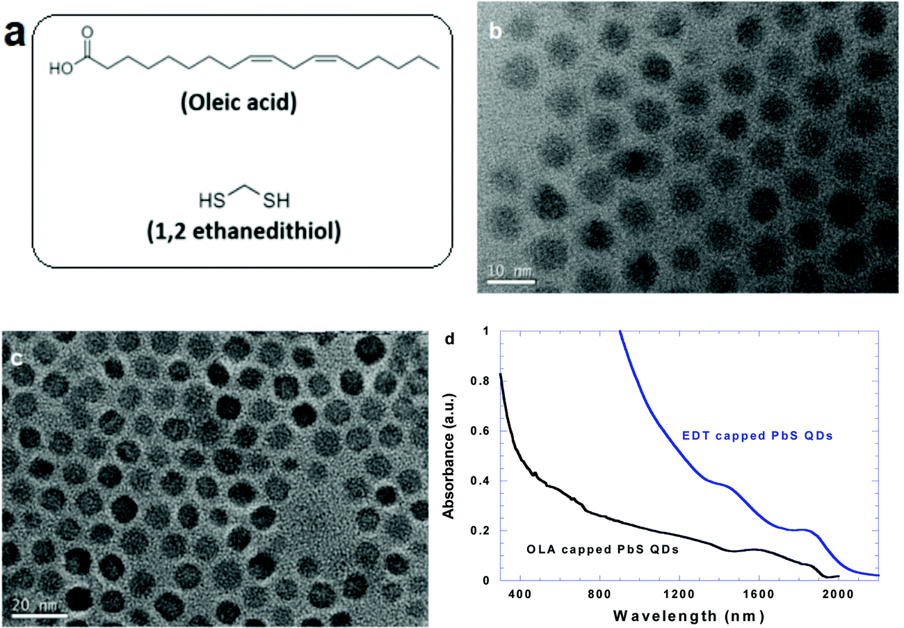 | ||
| Fig. 1 (a) Molecular structures of OLA and EDT, the TEM images of (b) the OLA-capped PbS QDs thin film and (c) the EDT-capped PbS QDs thin film, and (d) the absorption spectra of two different PbS QDs thin films. | ||
Fig. 1d presents the absorption spectra of PbS QDs. The absorption of the OLA-capped PbS QDs is extended to 1900 nm, whereas the absorption of the EDT-capped PbS QDs is extended to 2100 nm. Thus, the optical bandgap (Eg) is estimated to be 0.65 eV for the OLA-capped PbS QDs thin film and 0.59 eV for the EDT-capped PbS QDs thin film. According to the quantum confinement effect,56 the particle size of the OLA-capped PbS QDs is estimated to be ∼9 nm, whereas the particle size of the EDT-capped PbS QDs is estimated to be ∼13 nm. These results are in good agreement with the TEM images (Fig. 1b and c).
To verify the hypothesis that the EDT-capped PbS QDs thin film possess superior electronic properties than that of the OLA-capped PbS QDs, the TFTs are applied to study the field-effect mobilities of the two different PbS QDs thin films. The field-effect mobility in the saturation regime was extracted using the equation IDS = Ciμ (VGS − VTh)2W/2L,57 under the condition of −VDS > − (VGS − VTh), where IDS is the source/drain current, μ is the field-effect mobility, W is the channel width, L is the channel length, Ci is the capacitance per unit area of the gate dielectric layer, and VGS, VTh, and VDS are the gate, threshold, and source/drain voltages, respectively. Fig. 2a presents the IDSvs. VG characteristics of the TFTs made using two different PbS QDs thin films. The field-effect mobilities of ∼1 × 10⁻⁵ cm2 V−1 s−1 and ∼2.2 × 10⁻³ cm2 V−1 s−1 are observed from the OLA-capped PbS QDs thin film and the EDT-capped PbS QDs thin film, respectively. The field-effect hole mobility of the EDT-capped PbS QDs thin film is ∼100 times larger than that of the OLA-capped PbS QDs thin film. The enhanced charge carrier mobility of the EDT-capped PbS QDs thin film is ascribed to the short-chain of the EDT molecule.
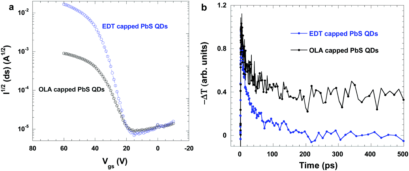 | ||
| Fig. 2 (a) The IDSversus VG characteristics of thin-film transistors based on the PbS QDs thin films, (b) the transient decay dynamics of PbS QDs thin films probed at 4.7 mm. | ||
Fig. 2b compares the dynamics of the photoinduced absorption in the OLA-capped PbS QDs thin film and the EDT-capped PbS QDs thin film probed at 4.7 mm. Compared to the OLA-capped PbS QDs, a fast decay from the EDT-capped PbS QDs thin film was observed. A slow decay indicates that the traps induced by the insulating OLA restrict electron hopping from one PbS QD to another. On the other hand, a fast decay observed from the EDT-capped PbS QDs reveals that the electron can hop from one PbS QDs to another with less restriction. These results demonstrate that the charge carrier mobility of the EDT-capped PbS QDs is higher than those of the OLA-capped PbS QDs.
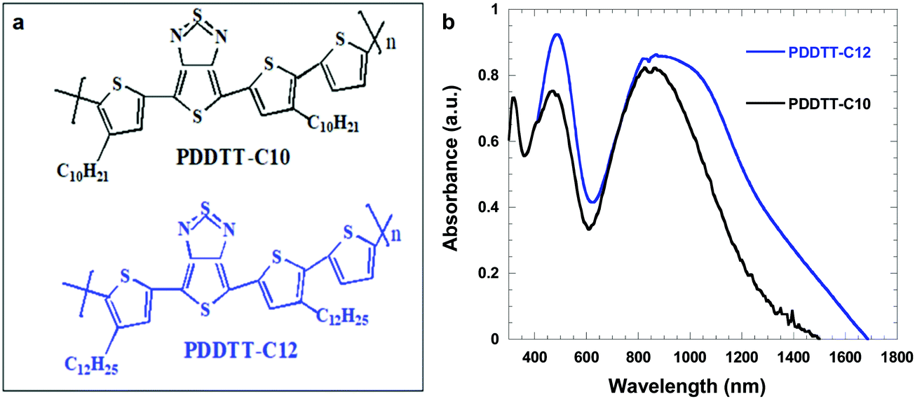
Fig. 3a presents the molecular structures of PDDTT with different side chains, where PDDTT is poly(5,7-bis(4-decanyl-2-thienyl)-thieno(3,4-b)diathiazole-thiophene-2,5). PDDTT is selected as the electron donor to form the bulk heterojunction (BHJ) composite with PbS QDs since it has a p-type low optical gap-conjugated polymer with decent charge carrier mobility.5 Moreover, PDDTT exhibits optical response up to the near-infrared (NIR) region, which could certainly contribute to the NIR spectral response for broadband PDs based on PDDTT composites.5 However, PDDTT with C10H21 side chain (PDDTT-C10) possesses poor solubility in typical organic solvents. To enhance its solubility, a side chain with a long carbon chain, such as C12H25 was incorporated with PDDTT. The synthetic procedures of PDDTT with the C12H25 side chain (PDDTT-C12) were the same as PDDTT-C10, which was reported previously.5,58 The absorption spectra of the PDDTT-C10 and PDDTT-C12 thin films are shown in Fig. 3b. Due to polymer aggregation,59 PDDTT-C12 thin film possesses extended absorption compared to the PDDTT-C10 thin film. Thus, PDDTT-C12 was used as the electron donor to form a BHJ composite with the EDT-capped PbS QDs for the development of broadband PDs.
 | ||
| Fig. 3 (a) Molecular structures and (b) absorption spectra of PDDTT with different side chains. | ||
Scheme 1a displays the device architecture of the broadband PDs. In this broadband PDs, neither ITO nor FTO, which are currently used as the transparent electrodes for various electronics, are used as the electrodes due to their very weak transmittance in the IR region.43–45 Moreover, carbon nanotubes (CNTs),45,46 silver nanowires (Ag NWs),47 and semiconducting polymers48–51 were also not utilized as the transparent electrodes since they possess poor electrical conductivity and are required to be processed with complicated costly nanoimprint lithography.45–49 Towards the end, an “inverted” device architecture, as shown in Scheme 1a, was developed. In this device structure, the Au/Cr bilayer is the anode, solution-processed MoO3 thin layer acts as the hole extraction layer (HEL), the PDDTT:PbS QDs BHJ composite thin film is the photoactive layer, the vacuum-deposited BaO thin layer acts as the electron extraction layer (EEL), thin Ba covered with Al bilayer acts as the cathode, and the transparent MgF2 layer is used as the passivation layer since it has excellent transparency from the UV-visible to the IR region.60 The Ba/Al (5 nm/20 nm) bilayer has decent transparency from the UV-visible to the IR region as well.61 BaO is a wide optical gap oxide. The light passing through the BaO EEL will be absorbed by the PDDTT:PbS QDs BHJ composite thin film. Moreover, smooth Au layer typical can reflect 30% of light.62Scheme 1b displays the absorption spectrum of the glass Cr/Au thin film. It is clear that the smooth Au thin layer could reflect light from 300 nm to 2000 nm. This reflected light can be further reabsorbed by the PDDTT:PbS QDs BHJ composite thin film, resulting in boosted photocurrent. As a result, a decent photocurrent is expected to be observed from the broadband PDs with a device structure shown in Scheme 1a.
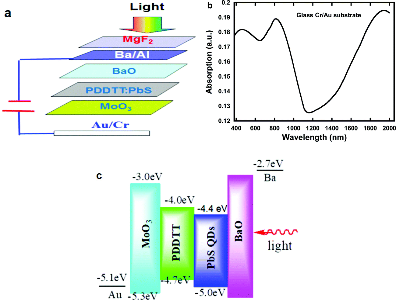 | ||
| Scheme 1 (a) Device architecture of broadband photodetectors, (b) the absorption spectrum of glass Cr/Au thin film, and (c) the LUMO and HOMO energy levels of MoO3, PDDTT, PbS QDs, BaO, and the work functions of the Au and Ba electrodes. | ||
Scheme 1c displays the lowest unoccupied molecular orbital (LUMO) and the highest occupied molecular orbital (HOMO) energy levels of MoO3, PDDTT, PbS QDs, BaO, and the work-functions of the Au and Ba electrodes. Without illumination, the Schottky barrier formed between the Au anode and the MoO3 HEL, and the Ba cathode and the BaO EEL could result in suppressed dark current density for broadband PDs. Under illumination, the excitons generated within the PDDTT:PbS QDs BHJ composite photoactive layer would dissociate into separated charge carriers under an external electric field created by the work function difference between the Au and Ba electrodes. Based on the band alignment, the separated electrons within the PDDTT:PbS QDs BHJ composite could transfer from PDDTT to PbS QDs due to a large LUMO offset between PDDTT and PbS QDs. These separated electrons are further extracted by the BaO HEL, and then collected by the Ba cathode. Meanwhile, the separated holes within the PDDTT:PbS QDs BHJ composite could transfer from PbS QDs to PDDTT due to a large HOMOs offset between the PbS QDs and PDDTT. These separated holes are further extracted by the MoO3 HEL, and then collected by the Au anode. Therefore, broadband PDs with a device structure shown in Fig. 1a would exhibit boosted R and D*.5
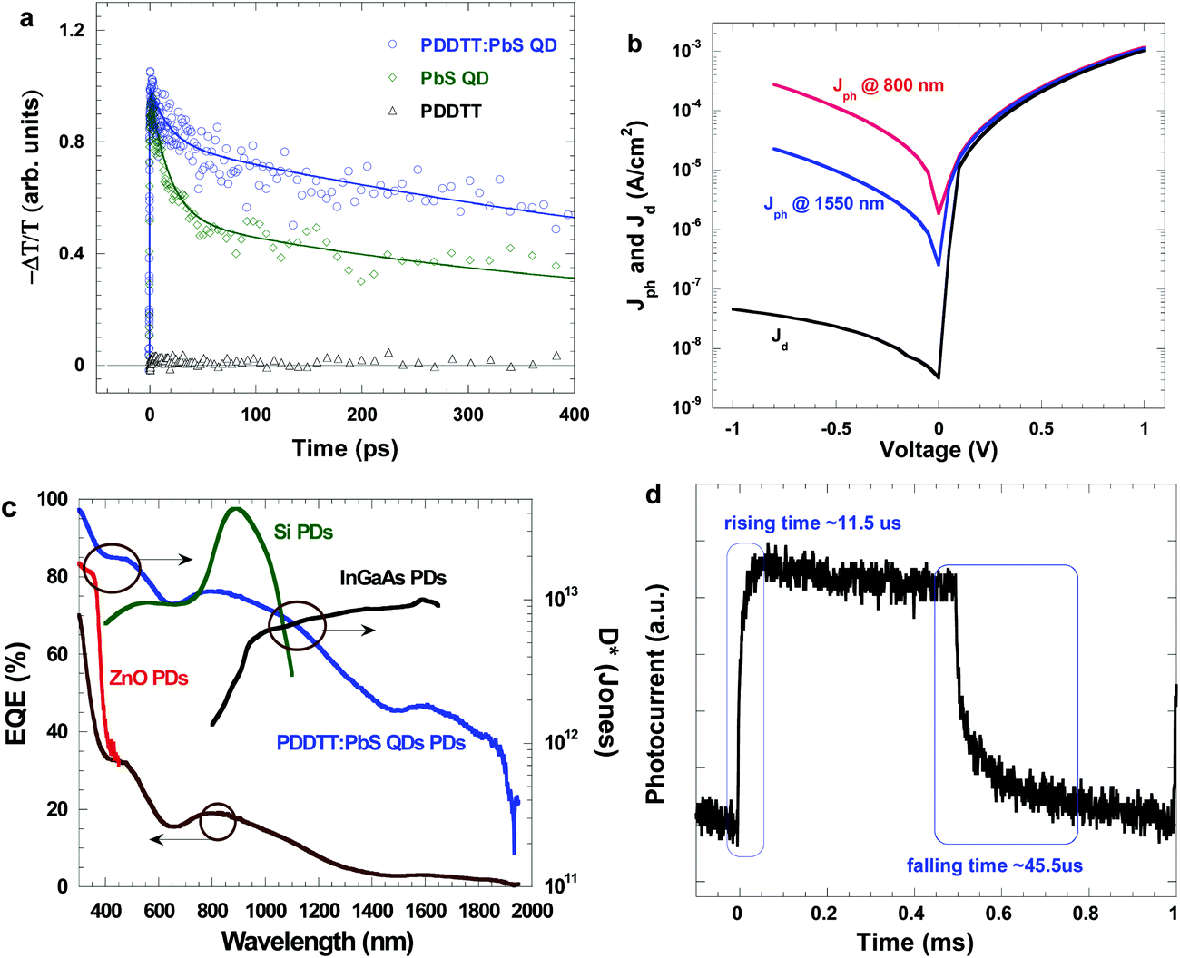
To verify the photoinduced charger transfer occurring within the PDDTT:PbS QDs BHJ composite, the dynamics of the photoinduced absorption in the PDDTT:PbS QDs BHJ composite thin film probed at 4.7 μm is investigated and further compared with those of pristine PDDTT and PbS QDs. The polarons from the conjugated polymers could be detected in the mid-IR spectral region.63–65 As indicated in Fig. 4a, a fast decay observed from the pristine PDDTT thin film indicates that the lifetime of the polarons from PDDTT is very short. A relatively slow decay observed from the EDT-capped PbS QDs indicates that the charge carrier is trapped due to the insulation of the EDT molecule. However, a much longer polaron lifetime, which is up to a nanosecond, is observed from the PDDTT:PbS QD BHJ composite thin film as compared to those from the pristine PDDTT thin film and the pristine PbS QD thin film. These results reveal that the long-lived mobile carriers show the integration of PDDTT and PbS QDs, and further demonstrate the efficient charge transfer from PDDTT to PbS QDs with inhibited back-transfer. Thus, as expected, broadband PDs based on the PDDTT:PbS QD BHJ composite thin film would exhibit high photocurrent.
 | ||
| Fig. 4 (a) The transient decay dynamics of PDDTT and PbS QDs thin films and PDDTT:PbS QDs BHJ composite thin film, (b) the J–V characteristics of broadband PDs, (c) the EQE spectrum of the broadband PDs and the projected detectivities of the broadband PDs versus wavelength compared with ZnO-based PDs, Si-based PDs, and InGaAs-based PDs, and (d) the photocurrent response time of broadband PDs. | ||
The current density versus voltage (J–V) characteristics of broadband PDs operated at RT and measured in dark and under a monochromatic light at a wavelength (λ) of 800 nm with a light intensity of 0.22 mW cm−2, and at a λ of 1550 nm with a light intensity of 0.05 mW cm−2, are shown in Fig. 4b. In dark, the broadband PDs exhibit asymmetric J–V characteristics with the ratification ratio of 2.5 × 10⁴ at ±1 V. These results indicate that the broadband PDs possess excellent photodiode behaviors.66 Different photocurrent densities observed from the broadband PDs under different monochromatic light illumination are ascribed to different light intensities, which indicate that the broadband PDs possess different photoresponsibilities.
Responsivity (R), described as R = Jph/Llight5,66 (where Jph is the photocurrent density and Llight is the light intensity), is often used to evaluate the device performance of the PDs. Under a bias of −0.1 V, R of 73 mA W−1 and 28.8 mA W−1 at λ of 800 nm and 1550 nm, respectively, are observed from the broadband PDs. Moreover, under a bias of −0.5 V, R of 545 mA W−1 and 195 mA W−1 at λ of 800 nm and 1550 nm, respectively, are observed from the broadband PDs.
If the dark current is only considered as the major contributor to the noise current,5,36,37 the project detectivity (D*) can be described as 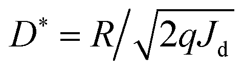 5 (where Jd is the dark current density, q is the elementary electric charge, q = 1.6 × 10⁻¹⁹ C, respectively). Thus, at RT, D* at λ of 800 nm and 1550 nm are calculated to be 1.6 × 10¹³ Jones and 6.4 × 10¹² Jones (cm Hz1/2/W), respectively, for the broadband PDs operated at a bias of −0.1 V. Moreover, at RT and under a bias of −0.5 V, D* at λ of 800 nm and 1550 nm was calculated to be 1.2 × 10¹⁴ Jones and 4.3 × 10¹³ Jones, respectively, for broadband PDs. These D* values are compatible with those observed from 2D metal dichalcogenide-based PDs.11–14 All these results certainly demonstrate that broadband PDs with a vertical device structure exhibit high R and D*, indicating that the broadband PDs have great potential applications.1–3
Fig. 4c presents the EQE spectrum of the broadband PDs. It is clear that the EQE spectrum of the broadband PDs is the superposition of the absorption spectra of the EDT-capped PbS QDs thin film (Fig. 1), PDDTT thin film (Fig. 3), and the reflection spectrum of the Au thin layer (Scheme 1b).
Based on the EQE spectrum and D* value at λ of 800 nm and 1550 nm for the broadband PDs, D* values versus wavelength are calculated based on 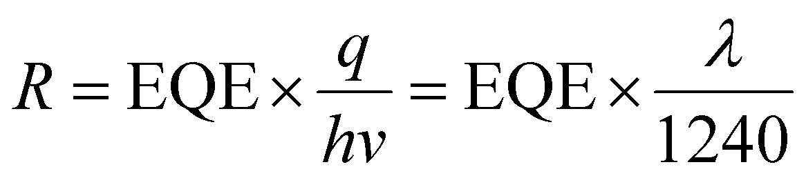 .5,66Fig. 4c presents D* versus wavelength for the broadband PDs. Under a bias of −0.1 V, the broadband PDs exhibit over 1012 Jones from 300 nm to 2000 nm at RT. Such decent D* over the broadband spectral region are ascribed to novel device architecture and the PDDTT:PbS QDs BHJ composite thin film.
The response time is another important parameter used to evaluate the device performance of the PDs. Fig. 4d presents the transient photocurrents of the broadband PDs. The rise time was defined as the time required for the output signals to increase from 10% to 90% of the saturated photocurrent. Similarly, the fall time was defined as the time required for the output signal to decrease from 90% to 10% of the saturated photocurrent.67,68 A rise time of 11 μs and a fall time of 45 μs was observed from the broadband PDs. Such slow response time is probably originated from the relatively poor electrical conductivity of the EDT-capped PbS QDs thin film.
4. Conclusion
Room-temperature operated, solution-processed broadband photodetectors (PDs) based on low optical gap conjugated polymer incorporated with highly electrically conductive PbS quantum dots (QDs) bulk heterojunction (BHJ) composite and inverted photodiode device structure without the incorporation of the transparent oxide electrodes, with the spectral response ranging from 300 nm to 2000 nm, were demonstrated. The low optical gap conjugated polymer, PDDTT, contributes to the IR photoresponse up to 1700 nm. PbS QDs further extend the IR photoresponse up to 2000 nm. The implementation of a photodiode with an “inverted” vertical device structure with the Au anode and the Ba/Al bilayer semitransparent cathode passivated with the MgF2 layer realize IR spectral response and circumvent the weak IR transparency of the transparent oxide electrodes. Photoinduced charge carrier transfer within the PDDTT:PbS QDs BHJ composite gave rise to the photocurrent, resulting in detectivities greater than 1012 Jones (cm Hz1/2/W) over the wavelength region from 300 nm to 2000 nm under a low applied bias. Thus, our findings of the utilization of the PDDTT:PbS QDs BHJ composites and an “inverted” vertical photodiode without the incorporation of the transparent oxide electrodes provide a facile way to realize broadband PDs.Conflicts of interest
We declare that we have no competing financial interest and all the financial support has been acknowledged in the manuscript.Acknowledgements
This contribution is dedicated to celebrating the 80th birthday of Professor Daoben Zhu, a great respectful scientist. We acknowledge National Science Foundation (EECS 1351785) for financial support. We also thank Professor Alan J. Heeger and his group for conducting ultrafast spectroscopy.References
- A. Rogalski, Material considerations for third generation infrared photon detectors, Infrared Phys. Technol., 2007, 50, 240–252 CrossRef CAS.
- A. R. Jha, A. Jha and D. A. Jha, IR technology: applications to electrooptics, photonic devices, and sensors, Wiley, New York, 2000 Search PubMed.
- A. Rogalski, HgCdTe IR detector material: history, status and outlook, Rep. Prog. Phys., 2005, 68, 2267–2336 CrossRef CAS.
- C. Liu, K. Wang, P. Du, E. Wang, X. Gong and A. J. Heeger, Ultrasensitive solution-processed broad-band photodetectors using CH3NH3PbI3 perovskite hybrids and PbS quantum dots as light harvesters, Nanoscale, 2015, 7, 16460–16469 RSC.
- X. Gong, M. Tong, Y. Xia, W. Cai, J. S. Moon, Y. Cao, G. Yu, C.-L. Shieh, B. Nilsson and A. J. Heeger, High-detectivity polymer photodetectors with spectral response from 300 nm to 1450 nm, Science, 2009, 325, 1665–1667 CrossRef CAS.
- G. Konstantatos and E. H. Sargent, Nanostructured materials for photon detection, Nat. Nanotechnol., 2010, 5, 391–400 CrossRef CAS PubMed.
- I. Moreels, Y. Justo, B. D. Geyter, M. K. Haustraete and Z. Hens, Z. Size-tunable, bright, and stable PbS quantum dots: a surface chemistry study, ACS Nano, 2011, 5, 2004–2012 CrossRef PubMed.
- C. Giansante, I. Infante, E. Fabiano, R. Grisorio, G. P. Suranna and G. Gigli, “Darker-than-Black” PbS quantum dots: enhancing optical absorption of colloidal semiconductor nanocrystals via short conjugated ligands, J. Am. Chem. Soc., 2015, 137, 1875–1886 CrossRef CAS PubMed.
- K. Qiao, H. Deng, X. Yang, D. Dong, M. Li, L. Hu, H. Liu, H. Song and J. Tang, Spectra-selective PbS quantum dot infrared photodetectors, Nanoscale, 2016, 8, 7137–7143 RSC.
- F. W. Wise, Lead salt quantum dots: the limit of strong quantum confinement, Acc. Chem. Res., 2000, 33, 773–780 CrossRef CAS.
- F. Xia, T. Mueller and Y.-M. Lin, A. Valdes-Garcia, P. Avouris, Ultrafast graphene photodetector, Nat. Nanotechnol., 2009, 4, 839–843 CrossRef CAS.
- C.-H. Liu, Y.-C. Chang, T. B. Norris and Z. Zhong, Graphene photodetectors with ultra-broadband and high responsivity at room temperature, Nat. Nanotechnol., 2014, 9, 273–278 CrossRef CAS PubMed.
- K. Zhang, T. Zhang, G. Cheng, T. Li, S. Wang, W. Wei, X. Zhou, W. Yu, Y. Sun, P. Wang, D. Zhang, C. Zeng, X. Wang, W. Hu, H. J. Fan, G. Shen, X. Chen, X. Duan, K. Chang and N. Dai, Interlayer transition and IR photodetection in atomically thin type-II MoTe2/MoS2 van der Waals heterostructures, ACS Nano, 2016, 10, 3852–3858 CrossRef CAS.
- Y. Xie, B. Zhang, S. Wang, D. Wang, A. Wang, Z. Wang, H. Yu, H. Zhang, Y. Chen, M. Zhao, B. Huang, L. Mei and J. Wang, Ultrabroadband MoS2 photodetector with spectral response from 445 to 2717 nm, Adv. Mater., 2017, 29, 1605972 CrossRef.
- N. S. Sariciftci, L. Smilowitz, A. J. Heeger and F. Wudl, Photoinduced electron transfer from a conducting polymer to buckminsterfullerene, Science, 1992, 1474–1476 CrossRef CAS.
- G. Yu, J. Gao, J. C. Hummelen, F. Wudl and A. J. Heeger, Polymer photovoltiac cells: Enhanced efficiencies via a network of internal donor-acceptor heterojunctions, Science, 1995, 270, 1789–1791 CrossRef CAS.
- L. Zheng, T. Zhu, W. Xu, L. Liu, J. Zheng, X. Gong and F. Wudl, Solution-processed broadband polymer photodetectors with a spectral response of up to 2.5 μm by a low bandgap donor–acceptor conjugated copolymer, J. Mater. Chem. C, 2018, 6, 3634–3641 RSC.
- J. Han, J. Qi, X. Zheng, Y. Wang, L. Hu, C. Guo, Y. Wang, Y. Li, D. Ma, W. Qiao and Z. Y. Wang, Low-bandgap donor–acceptor polymers for photodetectors with photoresponsivity from 300 nm to 1600 nm, J. Mater. Chem. C, 2017, 5, 159–165 RSC.
- L. Hu, J. Han, W. Qiao, X. Zhou, C. Wang, D. Ma, Y. Li and Z. Y. Wang, Side-chain engineering in naphthalenediimide-based n-type polymers for high-performance all-polymer photodetectors, Polym. Chem., 2018, 9, 327–334 RSC.
- L. Hu, W. Qiao, J. Han, X. Zhou, C. Wang, D. Ma, Z. Y. Wang and Y. Li, Naphthalene diimide–diketopyrrolopyrrole copolymers as non-fullerene acceptors for use in bulk-heterojunction all-polymer UV–NIR photodetectors, Polym. Chem., 2017, 8, 528–536 RSC.
- X. Wang, L. Lv, L. Li, Y. Chen, K. Zhang, H. Chen, H. Dong, J. Huang, G. Shen, Z. Yang and H. Huang, High-performance all-polymer photoresponse devices based on acceptor–acceptor conjugated polymers, Adv. Funct. Mater., 2016, 26, 6306–6315 CrossRef CAS.
- H. Wang, S. Xing, Y. Zheng, J. Kong, J. Yu and A. D. Taylor, Three-phase morphology evolution in sequentially solution-processed polymer photodetector: Toward low dark current and high photodetectivity, ACS Appl. Mater. Interfaces, 2018, 10, 3856–3864 CrossRef CAS.
- X. Hu, K. Wang, C. Liu, T. Meng, Y. Dong, S. Liu, F. Huang, X. Gong and Y. Cao, High-detectivity inverted near-infrared polymer photodetectors using cross-linkable conjugated polyfluorene as an electron extraction layer, J. Mater. Chem. C, 2014, 2, 9592–9598 RSC.
- X. Liu, J. Zhou, J. Zheng, M. L. Becker and X. Gong, Water-soluble CdTe quantum dots as an anode interlayer for solution-processed near infrared polymer photodetectors, Nanoscale, 2013, 5, 12474–12479 RSC.
- L. Zhang, T. Yang, L. Shen, Y. Fang, L. Dang, N. Zhou, X. Guo, Z. Hong, Y. Yang, H. Wu, J. Huang and Y. Liang, Toward highly sensitive polymer photodetectors by molecular engineering, Adv. Mater., 2015, 27, 6496–6503 CrossRef CAS PubMed.
- W. Wang, F. Zhang, L. Li, M. Gao and B. Hu, Improved performance of photomultiplication polymer photodetectors by adjustment of P3HT molecular arrangement, ACS Appl. Mater. Interfaces, 2015, 7, 22660–22668 CrossRef CAS.
- L. L. Li, F. J. Zhang, W. B. Wang, Q. S. An, J. Wang, Q. Q. Sun and M. Zhang, Trap-assisted photomultiplication polymer photodetectors obtaining an external quantum efficiency of 37
![[thin space (1/6-em)]](https://www.rsc.org/images/entities/char_2009.gif) 500%, ACS Appl. Mater. Interfaces, 2015, 7(10), 5890–5897 CrossRef CAS.
500%, ACS Appl. Mater. Interfaces, 2015, 7(10), 5890–5897 CrossRef CAS. - K. X. Yang, J. Wang, Z. J. Zhao, Z. J. Zhou, M. Liu, J. Zhang, Z. Q. He and F. J. Zhang, Smart strategy: transparent hole-transporting polymer as a regulator to optimize photomultiplication-type polymer photodetectors, ACS Appl. Mater. Interfaces, 2021, 13, 21565 CrossRef CAS PubMed.
- Z. J. Zhao, M. Liu, K. X. Yang, C. Y. Xu, Y. X. Guan, X. L. Ma, J. Wang and F. J. Zhang, Highly sensitive narrowband photomultiplication-type organic photodetectors prepared by transfer-printed technology, Adv. Funct. Mater., 2021, 2106009, DOI:10.1002/adfm.202106009.
- V. V. Diev, K. Hanson, J. D. Zimmerman, S. R. Forrest and M. E. Thompson, Fused pyrene-diporphyrins: shifting near-infrared absorption to 1.5 μm and beyond, Angew. Chem., Int. Ed., 2010, 49, 5523–5526 CrossRef CAS PubMed.
- E. Bundgaard and F. C. Krebs, Low band gap polymers for organic photovoltaics, Sol. Energy Mater. Sol. Cells, 2007, 91, 954–985 CrossRef CAS.
- E. Perzon, F. Zhang, M. Andersson, W. Mammo, O. Inganäs and M. R. Andersson, A conjugated polymer for near-infrared optoelectronic applications, Adv. Mater., 2007, 19, 3308–3311 CrossRef CAS.
- G. Konstantatos, J. Clifford, L. Levina and E. H. Sargent, Sensitive solution-processed visible-wavelength photodetectors, Nat. Photonics, 2007, 1, 531–534 CrossRef CAS.
- G. Konstantatos, I. Howard, A. Fischer, S. Hoogland, J. Clifford, E. Klem, L. Levina and E. H. Sargent, Ultrasensitive solution-cast quantum dot photodetectors, Nature, 2006, 442, 180–183 CrossRef CAS.
- C. Liu, K. Wang, C. Yi, X. Shi, P. Du, A. W. Smith, A. Karim and X. Gong, Ultrasensitive solution-processed perovskite hybrid photodetectors, J. Mater. Chem. C, 2015, 3, 6600–6606 RSC.
- C. Liu, K. Wang, P. Du, E. Wang, X. Gong and A. J. Heeger, Ultrasensitive solution-processed broad-band photodetectors using CH3NH3PbI3 perovskite hybrids and PbS quantum dots as light harvesters, Nanoscale, 2015, 7, 16460–16469 RSC.
- C. Liu, K. Wang, X. Gong and A. J. Heeger, Low bandgap semiconducting polymers for polymeric photovoltaics, Chem. Soc. Rev., 2016, 45, 4825–4846 RSC.
- C. Liu, H. Peng, K. Wang, C. Wei, Z. Wang and X. Gong, PbS quantum dots-induced trap-assisted charge injection in perovskite photodetectors, Nano Energy, 2016, 30, 27–35 CrossRef CAS.
- W. Xu, H. Peng, T. Zhu, C. Yi, L. Liu and X. Gong, A solution-processed near-infrared polymer: PbS quantum dot photodetectors, RSC Adv., 2017, 7, 34633–34637 RSC.
- L. Zheng, T. Zhu, W. Xu, J. Zheng, L. Liu and X. Gong, Ultrasensitive perovskite photodetectors by Co partially substituted hybrid perovskite, ACS Sustainable Chem. Eng., 2018, 6, 12055–12060 CrossRef CAS.
- T. Zhu, L. Zheng, X. Yao, L. Liu, F. Huang, Y. Cao and X. Gong, Ultrasensitive solution-processed broadband PbSe photodetectors through photomultiplication effect, ACS Appl. Mater. Interfaces, 2019, 11, 9205–9212 CrossRef CAS.
- T. Zhu, Y. Yang, L. Zheng, L. Liu, M. L. Becker and X. Gong, Solution-processed flexible broadband photodetectors with solution-processed transparent polymeric electrode, Adv. Funct. Mater., 2020, 30, 1909487 CrossRef CAS.
- B. D. Gates, Flexible electronics, Science, 2009, 323, 1566–1567 CrossRef CAS.
- D. Alemu, H.-Y. Wei, K.-C. Ho and C.-W. Chu, Highly conductive PEDOT:PSS electrode by simple film treatment with methanol for ITO-free polymer solar cells, Energy Environ. Sci., 2012, 5, 9662–9671 RSC.
- X. Mei and J. Ouyang, Highly conductive and transparent single-walled carbon nanotube thin films fabricated by gel coating, J. Mater. Chem., 2011, 21, 17842–17849 RSC.
- J. Du, S. Pei, L. Ma and H. M. Cheng, 25th Anniversary article: Carbon nanotube- and graphene-based transparent conductive films for optoelectronic devices, Adv. Mater., 2014, 26, 1958–1991 CrossRef CAS PubMed.
- Z. Yu, Q. Zhang, L. Li, Q. Chen, X. Niu, J. Liu and Q. Pei, Highly flexible silver nanowire electrodes for shape-memory polymer light-emitting diodes, Adv. Mater., 2011, 23, 664–668 CrossRef CAS.
- Y. Xia, K. Sun and J. Ouyang, Solution-processed metallic conducting polymer films as transparent electrode of optoelectronic devices, Adv. Mater., 2012, 24, 2436–2440 CrossRef CAS.
- Y. Xia, K. Sun and J. Ouyang, Highly conductive poly(3,4-ethylenedioxythiophene):poly(styrene sulfonate) films treated with an amphiphilic fluoro compound as the transparent electrode of polymer solar cells, Energy Environ. Sci., 2012, 5, 5325–5332 RSC.
- M. Vosgueritchian, D. J. Lipomi and Z. Bao, Highly conductive and transparent PEDOT:PSS films with a fluorosurfactant for stretchable and flexible transparent electrodes, Adv. Funct. Mater., 2012, 22, 421–428 CrossRef CAS.
- J. Ouyang, Solution-processed PEDOT:PSS films with conductivities as indium tin oxide through a treatment with mild and weak organic acids, ACS Appl. Mater. Interfaces, 2013, 5, 13082–13088 CrossRef CAS.
- M. Sykora, A. Y. Koposov, J. A. McGuire, R. K. Schulze, O. Tretiak, J. M. Pietryga and V. I. Klimov, Effect of air exposure on surface properties, electronic structure, and carrier relaxation in PbSe nanocrystals, ACS Nano, 2010, 4, 2021–2034 CrossRef CAS.
- D. K. Kim, Y. Lai, B. T. Diroll, C. B. Murray and C. R. Kagan, Flexible and low-voltage integrated circuits constructed from high-performance nanocrystal transistors, Nat. Commun., 2012, 3, 1216 CrossRef.
- A. Nag, M. V. Kovalenko, J.-S. Lee, W. Liu, B. Spokoyny and D. V. Talapin, Metal-free inorganic ligands for colloidal nanocrystals: S2−, HS−, Se2−, HSe−, Te2−, HTe−, TeS32−, OH−, and NH2− as surface ligands, J. Am. Chem. Soc., 2011, 133, 10612–10620 CrossRef CAS.
- A. T. Fafarman, W.-k. Koh, B. T. Diroll, D. K. Kim, D.-K. Ko, S. J. Oh, X. Ye, V. Doan-Nguyen, M. R. Crump, D. C. Reifsnyder, C. B. Murray and C. R. Kagan, Thiocyanate-capped nanocrystal colloids: vibrational reporter of surface chemistry and solution-based route to enhanced coupling in nanocrystal solids, J. Am. Chem. Soc., 2011, 133, 15753–15761 CrossRef CAS.
- T. Takagahara and K. Takeda, Theory of the quantum confinement effect on excitons in quantum dots of indirect-gap materials, Phys. Rev. B: Condens. Matter Mater. Phys., 1992, 46, 15578–15581 CrossRef CAS.
- H. Dong, H. Zhu, Q. Meng, X. Gong and W. Hu, Organic photoresponse materials and devices, Chem. Soc. Rev., 2012, 41, 1754–1808 RSC.
- Y. Xia, L. Wang, X. Deng, D. Li, X. Zhu and Y. Cao, Photocurrent response wavelength up to 1.1 μm from photovoltaic cells based on narrow-band-gap conjugated polymer and fullerene derivative, Appl. Phys. Lett., 2006, 89, 081106 CrossRef.
- T. Erb, U. Zhokhavets, G. Gobsch, S. Raleva, B. Stühn, P. Schilinsky, C. Waldauf and C. J. Brabec, Correlation between structural and optical properties of composite polymer/fullerene films for organic solar cells, Adv. Funct. Mater., 2005, 15, 1193–1196 CrossRef CAS.
- H. Krüger, E. Kemnitz, A. Hertwig and U. Beck, Transparent MgF2-films by sol-gel coating: Synthesis and optical properties, Thin Solid Films, 2008, 516, 4175–4177 CrossRef.
- D. W. Steuerman, A. Garcia, M. Dante, R. Yang, J. P. Löfvander and T.-Q. Nguyen, Imaging the interfaces of conjugated polymer optoelectronic devices, Adv. Mater., 2008, 20, 528–534 CrossRef CAS.
- D. R. Rainer, C. Xu, P. M. Holmblad and D. W. Goodman, Pd, Cu, and Au particles on Al2O3 thin films: an infrared reflection absorption spectroscopy study of monometallic and bimetallic planar model supported catalysts, J. Vac. Sci. Technol., A, 1997, 15, 1653–1662 CrossRef CAS.
- S. R. Cowan, A. Roy and A. J. Heeger, Recombination in polymer-fullerene bulk heterojunction solar cells, Phys. Rev. B: Condens. Matter Mater. Phys., 2010, 82, 245207 CrossRef.
- J. L. Bredas and G. B. Street, Polarons, bipolarons, and solitons in conducting polymers, Acc. Chem. Res., 1985, 18, 309–315 CrossRef CAS.
- C. Deibel, T. Strobel and V. Dyakonov, Origin of the efficient polaron-pair dissociation in polymer-fullerene blends, Phys. Rev. Lett., 2009, 103, 036402 CrossRef.
- S. M. Sze and K. K. Ng, Physics of Semiconductor Devices, John Wiley & Sons, Inc. 3rd edn, 2006 Search PubMed.
- Y. Wang, D. Yang, X. Zhou, D. Ma, A. Vadim, T. Ahamad and S. M. Alshehri, Perovskite/Polymer hybrid thin films for high external quantum efficiency photodetectors with wide spectral response from visible to near-infrared wavelengths, Adv. Opt. Mater., 2017, 5, 1700213 CrossRef.
- W. Xu, Y. Guo, X. Zhang, L. Zheng, T. Zhu, D. Zhao, W. Hu and X. Gong, Room-temperature-operated ultrasensitive broadband photodetectors by perovskite incorporated with conjugated polymer and single-wall carbon nanotubes, Adv. Funct. Mater., 2018, 28, 1705541 CrossRef.
Footnote |
| † These authors contributed to this work equally. |
| This journal is © The Royal Society of Chemistry 2022 |