A two-dimensional polymer memristor based on conformational changes with tunable resistive switching behaviours

Yaru Song a, Guangyuan Feng a, Lingli Wu *b, Enbing Zhang a, Chenfang Sun a, Dejuan Fa a, Qiu Liang a, Shengbin Lei *a, Xi Yu *a and Wenping Hu a
aTianjin Key Laboratory of Molecular Optoelectronic Science, Department of Chemistry, School of Science, Tianjin University, Tianjin 300072, P. R. China. E-mail: shengbin.lei@tju.edu.cn; xi.yu@tju.edu.cn
bMedical College, Northwest Minzu University, Lanzhou 730000, P. R. China. E-mail: wulingli19831106@163.com

Received 7th September 2021 , Accepted 28th October 2021

First published on 29th October 2021


Abstract

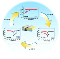
In this work, through rational monomer design we integrated the conformational change mechanism into a two-dimensional covalent polymer and implemented 3 different low-power memory behaviors on the same device by tuning the compliance current (ICC), including nonvolatile write-once-read-many-times (WORM) memory behaviour, nonvolatile FLASH memory behaviour and volatile dynamic random access memory (DRAM) behaviour. Furthermore, 2DP-based memory devices exhibit excellent flexibility and thermal stability, which is a desirable property for applications in wearable electronics and a high temperature environment. Finally, the conformation-induced conductance switching under an electric field was confirmed by UV-vis spectra. The differences in memory behaviour were attributed to the inherent differences in the degree of regioregularity and ease of the conformational relaxation of the field-induced rearrangement of carbazole groups.


Introduction

Resistive switching memory devices or memristors are considered to be the next-generation information storage and neuromorphic computing technologies due to their simple metal/insulator/metal sandwich structure, low fabrication cost, versatile ranges of material selection, fast read and write speed, low energy consumption, high retention performance and high switching endurance.1–9 Currently, the basic device mechanisms proposed for conductance switching include conductive filaments, charge transfer (CT), conformational changes, and trapping–detrapping.10–13 Very recently, our and other groups have reported the successful fabrication of 2DP-type memory devices based on the conductive filament mechanism and charge transfer mechanism.14–16 Nevertheless, the conformational change mechanism also plays an irreplaceable role in the construction of high-performance multifunctional memristors.17–22 At present, most active layers of memristors based on the conformational change mechanism are based on a one-dimensional (1D) polymer, and its internal structure is complex.23 In addition, a 1D polymer tends to pack densely, which is not conducive to the effective occurrence of the conformational change. And the stability of devices is poor and it is not easy to reduce the material thickness. Therefore, these factors limit the application of devices in terms of low power consumption, high temperature resistance, flexibility and high density integration. Compared with these commonly used 1D polymers, the framework structure of two-dimensional (2D) covalent polymers can anchor the conformational change groups and the porous framework can provide enough space for the conformational change, which will undoubtedly be beneficial to the occurrence of the conformational change, and further reduce the driving voltage, favourable for the realization of low power consumption devices. More importantly, 2D covalent polymers have the advantages of good chemical and thermal stability, intrinsic flexibility and self-supporting, adjustable thickness, green and convenient synthesis methods, etc.24–30 Therefore, 2D polymer films are ideal candidates for constructing high-performance devices.

Memory devices can show non-volatile (WORM and FLASH) and volatile (DRAM and SRAM) memory effects depending on whether electrical power is required to maintain a given state (ON state);31 both have great importance in applications such as for information storage or neuromorphic computing and beyond von-Neumann computer architectures.32 The memory behaviors of the device can be tuned by controlling the electrode type, doping, molecular structure and active layer and electrode thickness.33–39 Although there have been many reports, most of the multiple behaviors were achieved by controlling materials or electrodes during the preparation process. After the preparation is completed, it is not possible to change the memory behaviors anymore. Thus, there are still huge challenges in controllably and reversibly tuning the memory behavior of a given device.

Based on the above considerations, we propose a strategy to controllably adjust the resistive switching behavior of the same device by controlling the degree of conformational change of the active layer material. For this purpose we designed and synthesized the 2,5-bis(3-(9H-carbazol-9-yl)propoxy)terephthalaldehyde (TPAK) monomer (Fig. 1a), in which two carbazole groups are attached via a flexible spacer (O–C–C–C unit) to the phenyl backbone of terephthalaldehyde. Then the two-dimensional covalent polymer was synthesized by the Schiff base reaction between TPAK and 1,3,5-tris(4-aminophenyl)-benzene (TAPB). Under the effect of an electric field, the carbazole part will undergo conformational changes. When different compliance currents (ICC) are applied, the degree of conformational changes can be precisely adjusted, leading to different memory behaviors, including nonvolatile write-once-read-many-times (WORM) memory behaviour, nonvolatile FLASH memory behaviour and volatile dynamic random access memory (DRAM) behaviour. Moreover, the devices exhibit high thermal stability and excellent flexibility.


image file: d1tc04248c-f1.tif
Fig. 1 (a) The chemical structure of TAPB and TPAK monomers. (b) The STM image of 2DPTPAK+TAPB synthesized at the octanoic acid/HOPG interface. (c) OM, (d) AFM, (e) SEM, and (f) TEM images of the 2DPTPAK+TAPB film synthesized at the gas–liquid interface (inset: SAED image of the 2DP film).

Results and discussion

First, we demonstrated the rationality of TPAK molecular design through structural simulation and STM imaging. The molecular model shows that the carbazole groups have enough space to change the conformation in the 2DP framework, which has also been confirmed by the STM images of the 2DP, where the carbazole groups lie flat inside the pores of the network (Fig. 1b and Fig. S1, ESI). The TPAK molecule was synthesized by a two-step reaction (Fig. S2, ESI). The structure and purity of the product were confirmed by the 1H NMR spectrum, 13C NMR spectrum and high resolution mass spectra (Fig. S3–S7, ESI). Finally, highly uniform 2D covalent organic polymer films (2DPTPAK+TAPB) can be synthesized by condensation of TPAK with TAPB at the gas–liquid interface (Fig. S8, the detailed process is in the ESI).

The 2DP films obtained at the centimeter scale were transferred onto a Si/SiO2 substrate for morphology characterization through optical microscopy and atomic force microscopy (AFM). Using optical microscopy, the color of the film is uniform, which indicates that the film thickness is highly uniform (Fig. 1c). As shown in Fig. 1d, the average thickness and total surface roughness of the 2DPTPAK+TAPB film are about 30.5 ± 0.6 nm and 1.5 ± 0.2 nm, respectively. The scanning electron microscopy (SEM) image (Fig. 1e) shows that the films have good freestanding ability due to their covalently connected network structure. Transmission electron microscopy (TEM) and selected area electron diffraction (SAED) images (Fig. 1f and inset) show that the 2DPTPAK+TAPB thin films are amorphous, which is also consistent with the XRD data (Fig. S12a, ESI). This may suggest that the carbazole group is initially in a disordered state in the 2DPTPAK+TAPB film.

Due to its covalently bonded structure, the 2DPTPAK+TAPB film has good thermal stability in addition to the good freestanding ability. TGA data show that the 2DPTPAK+TAPB film is stable up to 360 °C, and the weight loss at 35–364 °C (8.8%) can be attributed to the loss of adsorbate and unreacted monomers (Fig. S9A, ESI). The rapid weight loss at 364–441 °C can be attributed to carbonization. AFM characterization of the samples before and after heating at 300 and 400 °C for 2 hours in a vacuum showed no significant change in morphology (Fig. S9B(b)–C(c), ESI) except for a slight decrease in thickness and surface roughness. In addition, the 2DPTPAK+TAPB film also exhibits excellent solvent resistance. After soaking in different organic solvents for 5 minutes, no significant changes in morphology, thickness and surface roughness were detected (Fig. S10a–f and 11A(a)–F(f), ESI). The excellent thermal stability and organic solvent resistance make the 2DPTPAK+TAPB film ideal for the fabrication of electronic devices that can operate in harsh environments.

The attenuated total reflectance FT-IR (ATR FTIR), Raman spectra and XPS spectra were used to further characterize the chemical structure of the 2DP films and confirmed the successful formation of the –C[double bond, length as m-dash]N bonds. Fig. 2a shows not only imine vibrations (1598 cm−1) but also the remaining carbonyl vibrations (1687 cm−1), indicating the formation of imine bonds and incomplete imine condensation.14,15 The Raman spectra (Fig. S12b, ESI) also provide evidence of imine formation in the 2DPTPAK+TAPB film. The band appearing at 1587 cm−1 indicates the imine stretching mode.14,15 And as shown in Fig. 2b, the N 1s spectrum of 2DPTPAK+TAPB can be separated into three components, the lower binding energy component centered at 398.9 eV can be attributed to the imine bonds, the one at 399.9 eV correspond to the unreacted –NH2 of TAPB and the one at 400.4 eV is from the carbazole-N, which clearly confirms the formation of imine bonds and the incomplete reaction of the precursors, which is consistent with the FT-IR results. The UV-vis absorption spectra of the 2DPTPAK+TAPB film, and TAPB and TPAK monomers are shown in Fig. 2c and Fig. S13 (ESI). The onset of the absorption peak of the 2DPTPAK+TAPB film is determined to be 500 nm, from which the optical bandgap (Eeg) was calculated to be approximately 2.48 eV. In combination with cyclic voltammetry (CV) (Fig. 2d and e), the energy levels of the highest occupied molecular orbital (HOMO) and lowest unoccupied molecular orbital (LUMO) of the 2DPTPAK+TAPB film were determined to be −5.51 eV and −3.03 eV, respectively. This favours the injection of holes instead of electrons. As seen in the energy diagram (Fig. 2f), the barrier of hole injection (0.71 eV) is much smaller than the barrier of electron injection (2.07 eV). Thus, the switching of the device was observed in the positive bias, with the transport of holes as the conducting mechanism.


image file: d1tc04248c-f2.tif
Fig. 2 (a) IR spectra of 2DPTPAK+TAPB. (b) XPS N 1s spectra of 2DPTPAK+TAPB. (c) UV-Vis spectra of the 2DPTPAK+TAPB film (Eeg = hc/λ = 1240/500 = 2.48 eV). (d) and (e) CV curve of the ferrocene standard and 2DPTPAK+TAPB film. The CV curve of the ferrocene standard, swept under the same conditions as for the film. EFOC was measured to be 0.44 eV vs. Ag/AgCl in CH3CN. EHOMO = −[Eox(onset)vs.Ag/AgCl + 4.8 − EFOC] = −5.51 eV; ELUMO = EHOMO + Eeg = −3.03 eV. (f) Schematic energy diagram of an Au/2DP/ITO structure.

The memory device with a sandwich structure of Au/2DPTPAK+TAPB/ITO was fabricated and the performance was investigated under ambient conditions. An inert Au electrode was used as the top electrode instead of the active Ag and Al electrodes, which rules out the possibility for the electrochemical metallization mechanism. As shown in Fig. 3a, when the ICC is set at 10−4 A, the device switches from the OFF state to ON state at about 1.26 V during the IV measurement from 0 V → 3.0 V → 0 V (sweep 1). However, after turning off the power, the memory device can only remain at the ON state for several tens of seconds after which it automatically relaxes to a high resistance state. And then, it can continue to be switched to the ON state again by applying the appropriate voltage (sweep 2). For the DRAM effect, the ON state could be retained for a short period after the removal of the applied voltage.31 Therefore, the behaviour of the Au/2DPTPAK+TAPB/ITO device shows characteristics of dynamic random access memory (DRAM). To explore the switching uniformity of the prepared device, IV curves of about 70 devices were measured. The device-to-device distributions of HRS resistance and LRS resistance range from 8.8 × 10⁴ to 8.3 × 10⁵ Ω and 9.2 × 10² to 3.8 × 10³ Ω (read at 0.1 V), respectively (Fig. 3d). Thus, the calculated ON/OFF ratio is about 102. In order to evaluate the retention time of the ON state of the Au/2DPTPAK+TAPB/ITO device, the It curve was measured at 0.1 V read voltage at room temperature (the inset of Fig. 3g). The retention time of the device was concentrated in the range of 20–40 s, which further indicates that when the ICC is set at 10−4 A, the device exhibits the switching characteristics of DRAM (Fig. 3g).


image file: d1tc04248c-f3.tif
Fig. 3 (a, b and c) IV characteristics of the Au/2DPTPAK+TAPB/ITO device when the ICC is 10−4 A, 10−3 A and 10−1 A, respectively (inset: a schematic illustration of the Au/2DP/ITO device). (d, e and f) The device-to-device distributions of HRS resistance and LRS resistance (read at 0.1 V) when the ICC is 10−4 A, 10−3 A and 10−1 A, respectively. (g) Retention time of the Au/2DPTPAK+TAPB/ITO device when the ICC is 10−4 A (inset: It curve of the Au/2DPTPAK+TAPB/ITO device). (h and i) Retention time of the Au/2DPTPAK+TAPB/ITO device (read at 0.1 V) when the ICC is 10−3 A and 10−1 A, respectively. The thickness of the active layer (2DPTPAK+TAPB) of the above devices is about 20–30 nm.

Fig. 3b shows that when the ICC is set at 10−3 A, the device switches from the OFF state to ON state at about 1.36 V during the IV measurement from 0 V → 3.0 V → 0 V (sweep 1). By an inverse sweep from 0 V → −3.0 V → 0 V (sweep 2, ICC = 10−1 A), a switch from high-conductivity (ON) state to a low-conductivity (OFF) state was observed. Bias is not required to sustain the high-conductivity state. However, only a suitable negative bias can switch the high-conductivity state to the low-conductivity state. This feature is consistent with flash memory behaviors. To explore the switching uniformity of the prepared device, IV curves of about 50 devices were measured. The device-to-device distributions of HRS resistance and LRS resistance range from 2.0 × 10⁵ to 5.5 × 10⁵ Ω and 1.7 × 10² to 4.8 × 10² Ω (read at 0.1 V), respectively (Fig. 3e). And the ON/OFF ratio is about 103. As shown in Fig. 3i, the retention characteristic of the Au/2DPTPAK+TAPB/ITO devices was measured at 0.1 V read voltage at room temperature. The resistances of both states show no obvious change for about 3.5 × 10³ s indicating that our devices have a relatively good stability. We explored the device stability during multiple write and erase operations. As shown in Fig. S14 (ESI), we have performed about 100 write and erase operations, and the device can still work normally, and the HRS resistance and LRS resistance are evenly distributed.

As shown in Fig. 3c, when the ICC is set at 10−1 A, the device switches from the low-conductivity (OFF) state to the high-conductivity (ON) state at about 1.52 V during the IV measurement from 0 V → 3.0 V → 0 V (sweep 1). The device cannot be switched back to its OFF state by subsequent application of a negative bias (sweep 2, ICC = 10−1 A) or a positive bias (sweep 3). The device remains in the ON state even after the power has been turned off. Thus, the Au/2DPTPAK+TAPB/ITO device exhibits write-once-read-many-times (WORM) memory behaviour, as it is both non-rewritable and nonvolatile after it has been switched ON. In addition, the device has an ON/OFF ratio of up to 103 when read at 0.1 V. To explore the switching uniformity of the prepared device, IV curves of about 50 devices were measured. The device-to-device distributions of HRS resistance and LRS resistance range from 2.1 × 10⁴ to 7.5 × 10⁴ Ω and 3.2 × 101 to 7.7 × 101 Ω (read at 0.1 V), respectively (Fig. 3f). To evaluate the persistence of the ON/OFF states of the Au/2DPTPAK+TAPB/ITO devices, the retention characteristic was measured at 0.1 V read voltage at room temperature, as shown in Fig. 3i. The resistances of both states show no obvious change for about 3.0 × 10³ s, indicating that our devices have a relatively good stability.

So far, most of the memory devices based on the mechanism of conformational changes have only worked at room temperature, showing limited heat resistance, because the functional layers in memristors based on traditional organic molecules and polymers are mostly stabilized through intermolecular interactions. In our devices, we speculate that the high thermal stability of the 2DPTPAK+TAPB film makes it an ideal material for fabricating devices with high thermal stability. To further evaluate the thermal stability of the device, we heated an RS device made with a 25.5 ± 0.5 nm thick 2DPTPAK+TAPB film for 2 hours at different temperatures in an argon-protected cube oven. The switching characteristics and success rate after heating are shown in Fig. 4a–c. Devices based on 2DPTPAK+TAPB at different limiting currents exhibit reliable non-volatile and volatile storage properties even after annealing at 300 °C. The HRS and LRS resistance of the device did not change significantly with increasing annealing temperature. After annealing at 300 °C, the success rate was only slightly reduced to 70%, indicating that the 2DPTPAK+TAPB based device still showed high reliability after heating at 300 °C. Only after annealing at 400 °C, the success rate suddenly drops to 10%, and most devices cannot operate. The high thermal stability is attributed to the strong covalent bonds in the 2DPTPAK+TAPB film. This will have potential applications in electronic devices under harsh conditions such as in the aerospace, geothermal, oil and gas industries, as well as in implanted devices. Furthermore, we were able to fabricate RS devices with ultra-thin 2DPTPAK+TAPB films down to 2.7 ± 0.5 nm, in which different switching behaviors such as the volatile dynamic random access (DRAM) memory feature, nonvolatile FLASH memory feature and the nonvolatile write-once-read-many-times (WORM) memory feature can still be realized by adjusting the ICC to 10−4 A, 10−3 A and 10−1 A, respectively. And the devices have an on/off ratio of about 4 at a 0.1 V read voltage (Fig. 4d–f). This ultra-thin device will facilitate the integrated application in flexible and wearable devices.


image file: d1tc04248c-f4.tif
Fig. 4 (a, b and c) (left) The HRS and LRS states and (right) the success rate of a Au/2DPTPAK+TAPB/ITO device (about 20–30 nm) (read at 0.1 V) measured at different temperatures when the ICC is 10−4 A, 10−3 A and 10−1 A, respectively. (d), (e) and (f) IV Characteristics of a Au/2DPTPAK+TAPB/ITO device with a 2.7 ± 0.5 nm thick 2DPTPAK+TAPB film when the ICC is 10−4 A, 10−3 A and 10−1 A, respectively (inset: a schematic illustration of the Au/2DP/ITO device). (g), (h) and (i) Switching curves of a flexible Au/2DPTPAK+TAPB/ITO device before and after repeated mechanical bending when the ICC is 10−4 A, 10−3 A and 10−1 A, respectively (inset: a photograph of the flexible device).

Flexible devices have generated a lot of research interest due to their potential applications in wearable electronics, smart skin and minimally invasive biomedical devices. From previous data we demonstrated the high flexibility and uniformity of the 2DPTPAK+TAPB films, which will be ideal for flexible equipment applications. Here, we show a flexible device with a vertical Au/2DPTPAK+TAPB/ITO structure on a flexible (ITO) substrate (Fig. 4g–i). The thickness of the 2DPTPAK+TAPB film was 26.5 ± 0.5 nm. The flexible memory devices can also realize the adjustment of switching behavior by setting the current compliance to 10−4 A, 10−3 A and 10−1 A, respectively and maintaining the memory characteristics after 500 bending cycles. Finally, the devices failed to operate until 1000 bending cycles. The flexible device exhibits excellent mechanical durability, and therefore, the 2DPTPAK+TAPB film with good flexibility and high thermal stability is very attractive for the application of a flexible device under harsh conditions.

The carbazole groups are electron donor and hole transporters40,41 and tend to form a partial or complete face-to-face conformation with adjacent carbazole groups, resulting in extended electron delocalization. The stacked carbazole groups provide a charge-carrier hopping pathway in the direction of the electric field.40 We speculate that the switching effect in the Au/2DPTPAK+TAPB/ITO device may be due to the change in the conformation of the carbazole groups through the rotation of these groups, resulting in more regular π–π stacking regions. At low applied voltages, the carbazole pendant groups attached to the backbone through the flexible C–O bonds in TPAK are initially in random orientation, as shown by the simulated structure in the left image of Fig. 5c. Upon application of a voltage, the injected holes oxidize the carbazole group near the interface to form a positively charged species. As a potent electron donor, a nearby neutral carbazole group may interact with a positively charged carbazole group for charge transfer or excess acceptor interaction with a nearby carbazole group to form a partial or complete face-to-face conformation, as shown in the right image of Fig. 5c. And then it will delocalize the positive charge to the adjacent ordered carbazole group. This process can then be propagated through the polymer film. When the applied voltage exceeds a threshold, a significant portion of the carbazole groups undergo this conformational change, resulting in enhanced charge transport through neighboring, aligned carbazole groups, producing a high conductivity state (ON state).42 The UV-visible spectra of the 2DPTPAK+TAPB film in the “OFF” state and “ON” state give evidence for the conformational change. As shown in Fig. 5a, a liquid Ga–In droplet instead of an Au electrode was used to construct a vertical structured Ga–In/2DP/ITO device; when a 3.0 V voltage scan was applied with ICC set at 10−4 A, 10−3 A and 10−1 A, respectively, slight but significant red shifts were seen (Fig. 5b). This was attributed to the increased interaction between the carbazole groups in the face-to-face conformation.43 In order to further rule out the possibility that the red-shift phenomenon solely comes from the contact between the film and the Ga–In liquid electrode, we tested the UV spectrum of the film in contact with the Ga–In liquid electrode but without applying voltage (Fig. S15, ESI), and no red-shift was found, which further illustrates that the red-shift phenomenon comes from the conformational change of the carbazole groups after the voltage was applied. Moreover, the conformation change of 2DPTPAK+TAPB in different states is also supported by the results of fluorescence. As shown in Fig. S16 (ESI), the main emission peaks of 2DPTPAK+TAPB in ON and OFF states both appear at around 370 and 525 nm. The excimeric species of the over-lapped (face-to-face conformation) carbazole groups show emissions at about 370 and 420 nm owing to the higher-energy excimer and sandwich-like excimer, respectively.12,21 After applying voltage to the film, the ON state of 2DPTPAK+TAPB shows a stronger emission and a slight red shift to 376 nm compared with the OFF state (372 nm), which is due to the increased interaction among the carbazole groups in a face-to-face conformation. A similar phenomenon is also observed in the emission at approximately 420 nm. The STM characterization also gives some more direct evidence for the conformational change. As shown in Fig. S17a and b (ESI), at a bias voltage of −0.3 V, the carbazole groups can be observed in the STM image (the positions of the carbazole groups were marked by the red circles), but when increasing the bias voltage to −0.6 V, the carbazole groups were never observable anymore, which was attributed to the conformational change of the carbazole group.


image file: d1tc04248c-f5.tif
Fig. 5 (a) The schematic of the Ga–In/2DP/ITO device. (b) The UV-vis spectra of the device in different “ON” states and “OFF” state. (c) The proposed conformation change memory mechanism.

To further explore the conduction mechanism of resistance switching, a typical IV curve of the device is plotted using a double logarithmic scale, as shown in Fig. S19–S21 (ESI). The OFF state IV characteristic of the device at 3 different compliance currents can be well fitted with the combination of the Schottky emission model and the space charge limited current model with field dependent mobility.44–46 In the low voltage range from 0 to 0.5 V, the ln[thin space (1/6-em)]I–ln[thin space (1/6-em)]V characteristic shows a linear relationship corresponding to the space charge limited current model (Fig. S19–S21b, ESI), while in the high voltage region of HRS (0.5 V to Vset), the ln[thin space (1/6-em)]I–ln[thin space (1/6-em)]V curve shows a nonlinear relationship. Further analysis shows a linear relationship between ln[thin space (1/6-em)]I and V1/2, indicating that the Schottky emission is the main conduction mechanism of the HRS in the high voltage region (Fig. S19–S21c, ESI). The IV characteristic of the ON state shows a linear plot with a slope of 1 (Fig. S19–S21d, ESI), indicating ohmic behaviour. Furthermore, the suitability of the fitted model was confirmed by the temperature dependence of the device current. The ON state current of the device shows the temperature dependence (Fig. S22b, d and f, ESI). And the negative temperature coefficient indicates the corresponding non-metallic conductive channel, which is consistent with most reported literature on the mechanism of conformational changes.

We believe that the mechanism for the tunable memory behaviours by adjusting the applied ICC is due to the effect on the degree of conformational changes. Since our carbazole-containing 2D polymer device is based on conformational changes mechanism, once conductive paths are formed under the applied electric field, the charge transfer will be promoted under biases. The degree of conformational change that occurs also increases with the increase of applied bias. With the maximum compliance current the degree of conformational change is very high, and the formed conductive channel is robust, so after the device is switched to the “ON” state, it cannot be returned to the “OFF” state by applying a reverse bias or the same bias voltage. However, under a small compliance current, the degree of conformational change is not high, and the organic framework of 2DP provides sufficient conformational freedom, thus the device can return to the “OFF” state through conformational relaxation. Finally, the degree of conformational change that occurs at a moderate compliance current is between the first two, so it can be returned to the “OFF” state by applying a reverse bias. These explanations are supported by the UV-visible spectra. As shown in Fig. 5b and Fig. S18, Table S1 (ESI), the UV-vis spectrum of the three different ON states of the device shows different degrees of red shifts. Among them, the degree of the red shift in the WORM state is the largest (19 nm), followed by the FLASH state (9 nm), and the degree of the red shift in the DRAM state is the smallest (5 nm), corresponding to different degrees of conformational changes. In short, the free space provided by the rigid 2D polymer backbone is a key for the success of the tunable memory behavior of our conformational change 2DP memristor.

Conclusions

In summary, a resistive switching memory device based on the 2DPTPAK+TAPB film with the conformational change mechanism was prepared. The memory behaviours of the 2DPTPAK+TAPB-based devices can be adjusted by the compliance current (ICC). When the ICC is 10−1 A, the device exhibits a non-volatile write-once-read-many-times (WORM) memory behaviour with a large ON/OFF ratio of 103 and a long retention time of 3.0 × 10³ s. When the ICC is 10−3 A, the devices show nonvolatile FLASH memory behaviour with an ON/OFF ratio of 103 and a long retention time of 3.5 × 10³ s. However, when the ICC is 10−4 A, the device exhibits volatile dynamic random access memory (DRAM) behaviour with an ON/OFF ratio of 102 and a retention time of 20–40 s. Furthermore, 2DPTPAK+TAPB-based memory devices exhibit excellent flexibility and thermal stability. Compared with other works, this work extended the conformational change mechanism to two-dimensional polymers, and achieved three different types of memory behaviours on the same device with low turn on voltage and ultra-thin active layer, and the memory behavior can be easily tuned by adjusting the compliance current (Tables S2 and S3, ESI).

Conflicts of interest

There are no conflicts to declare.

Acknowledgements

This work was financially supported by the National Science Foundation of China (21572157, 21872103, and 51633006) and the Ministry of Science and Technology of China (Grants 2016YFB0401100).

Notes and references

  1. D. B. Strukov, G. S. Snider, D. R. Stewart and R. S. Williams, Nature, 2008, 453, 80–83 CrossRef CAS PubMed.
  2. M. Wang, S. Cai, C. Pan, C. Wang, X. Lian, Y. Zhuo, K. Xu, T. Cao, X. Pan, B. Wang, S. J. Liang, J. J. Yang, P. Wang and F. Miao, Nat. Electron., 2018, 1, 130–136 CrossRef CAS.
  3. Z. Wang, S. Joshi, S. E. Savel’ev, H. Jiang, R. Midya, P. Lin, M. Hu, N. Ge, J. P. Strachan, Z. Li, Q. Wu, M. Barnell, G. L. Li, H. L. Xin, R. S. Williams, Q. Xia and J. J. Yang, Nat. Mater., 2016, 16, 101–108 CrossRef PubMed.
  4. L. Chua, Appl. Phys. A: Mater. Sci. Process., 2011, 102, 765–783 CrossRef CAS.
  5. R. Waser, R. Dittmann, G. Staikov and K. Szot, Adv. Mater., 2009, 21, 2632–2663 CrossRef CAS.
  6. L. J. Wei, Z. Z. Hu, G. X. Du, Y. Yuan, J. Wang, H. Q. Tu, B. You, S. M. Zhou, J. T. Qu, H. W. Liu, R. K. Zheng, Y. Hu and J. Du, Adv. Mater., 2018, 30, 1801885 CrossRef.
  7. L. F. Hu, W. T. Han and H. Wang, Nanotechnology, 2020, 31, 155202 CrossRef CAS.
  8. S. Roy, G. Niu, Q. Wang, Y. K. Wang, Y. J. Zhang, H. P. Wu, S. J. Zhai, P. Shi, S. N. Song, Z. T. Song, Z. G. Ye, C. Wenger, T. Schroeder, Y. H. Xie, X. J. Meng, W. B. Luo and W. Ren, ACS Appl. Mater. Interfaces, 2020, 12, 10648–10656 CrossRef CAS.
  9. F. X. Yang, L. J. Sun, Q. X. Duan, H. L. Dong, Z. K. Jing, Y. C. Yang, R. J. Li, X. T. Zhang, W. P. Hu and L. Chua, Smart Mater., 2021, 2, 99–108 Search PubMed.
  10. S. P. Park, Y. J. Tak, H. J. Kim, J. H. Lee, H. Yoo and H. J. Kim, Adv. Mater., 2018, 30, 1800722 CrossRef.
  11. H. Li, Z. N. Jin, N. J. Li, Q. F. Xu, H. W. Gu, J. M. Lu, X. W. Xia and L. H. Wang, J. Mater. Chem., 2011, 21, 5860–5862 RSC.
  12. S. L. Lim, Q. Ling, E. Y. H. Teo, C. X. Zhu, D. S. H. Chan, E. T. Kang and K. G. Neoh, Chem. Mater., 2007, 19, 5148–5157 CrossRef CAS.
  13. J. Lee, E. Lee, S. Kim., G. S. Bang, D. A. Shultz, R. D. Schmidt, M. D. E. Forbes and H. Lee, Angew. Chem., Int. Ed., 2011, 50, 4414–4418 CrossRef CAS.
  14. J. Liu, F. X. Yang, L. L. Cao, B. L. Li, K. Yuan, S. B. Lei and W. P. Hu, Adv. Mater., 2019, 31, 1902264 CrossRef.
  15. Y. R. Song, J. Liu, W. H. Li, L. Liu, L. Yang, S. B. Lei and W. P. Hu, Chem. Commun., 2020, 56, 6356–6359 RSC.
  16. B. Sun, X. L. Li, T. T. Feng, S. L. Cai, T. Chen, C. H. Zhu, J. Zhang, D. Wang and Y. Liu, ACS Appl. Mater. Interfaces, 2020, 12, 51837–51845 CrossRef CAS.
  17. D. W. He, H. Zhuang, H. F. Liu, H. Z. Liu, H. Li and J. M. Lu, J. Mater. Chem. C, 2013, 1, 7883–7889 RSC.
  18. Z. Li, M. Wang, H. Li, J. H. He, N. J. Li, Q. F. Xua and J. M. Lu, J. Mater. Chem. C, 2017, 5, 8593–8598 RSC.
  19. E. Y. H. Teo, Q. D. Ling, Y. Song, Y. P. Tan, W. Wang, E. T. Kang, D. S. H. Chan and C. X. Zhua, Org. Electron., 2006, 7, 173–180 CrossRef CAS.
  20. L. H. Xie, Q. D. Ling, X. Y. Hou and W. Huang, J. Am. Chem. Soc., 2008, 130, 2120–2121 CrossRef CAS PubMed.
  21. Y. H. Liu, N. J. Li, X. W. Xia, Q. F. Xu, J. F. Ge and J. M. Lu, Mater. Chem. Phys., 2010, 123, 685–689 CrossRef CAS.
  22. A. Bandyopadhyay and A. J. Pal, Appl. Phys. Lett., 2004, 84, 999–1001 CrossRef CAS.
  23. Q. D. Ling, D. J. Li, C. X. Zhu, D. S. H. Chan, E. T. Kang and K. G. Neoh, Prog. Polym. Sci., 2008, 33, 917–978 CrossRef CAS.
  24. Y. X. Yu, J. B. Lin and S. B. Lei, RSC Adv., 2017, 7, 11496 RSC.
  25. X. D. Zhuang, Y. Y. Mai, D. Q. Wu, F. Zhang and X. L. Feng, Adv. Mater., 2015, 27, 403–427 CrossRef CAS PubMed.
  26. H. Liu, Y. S. Wang, Z. S. Qin, D. Liu, H. Xu, H. L. Dong and W. P. Hu, J. Phys. Chem. Lett., 2021, 12, 1612–1630 CrossRef CAS.
  27. J. Y. Ouyang, Smart Mater., 2021, 2, 263–285 Search PubMed.
  28. C. G. Li, Y. S. Wang, Y. Zou, X. T. Zhang, H. L. Dong and W. P. Hu, Angew. Chem., Int. Ed., 2020, 59, 9403–9407 CrossRef CAS PubMed.
  29. C. G. Li, Y. S. Wang, H. L. Dong, X. T. Zhang and W. P. Hu, Sci. China Mater., 2020, 63, 172–176 CrossRef.
  30. Q. Zhang, H. L. Dong and W. P. Hu, J. Mater. Chem. C, 2018, 6, 10672–10686 RSC.
  31. W. P. Lin, S. J. Liu, T. Gong, Q. Zhao and W. Huang, Adv. Mater., 2014, 26, 570–606 CrossRef CAS.
  32. C. C. Zhang, J. Shang, W. H. Xue, H. W. Tan, L. Pan, X. Yang, S. S. Guo, J. Hao, G. Liu and R. W. Li, Chem. Commun., 2016, 52, 4828–4831 RSC.
  33. G. T. S. How, N. A. Talik, Y. B. Kar, H. Nakajima, S. Tunmee and G. B. Tong, Appl. Surf. Sci., 2019, 473, 194–202 CrossRef CAS.
  34. H. Y. Du, J. H. Chen, M. L. Tu, S. W. Luo, S. D. Li, S. G. Yuan, T. X. Gong, W. Huang, W. J. Jie and J. H. Hao, J. Mater. Chem. C, 2019, 7, 12160–12169 RSC.
  35. M. Yang, D. H. Bao and S. W. Li, J. Phys. D: Appl. Phys., 2013, 46, 495111 CrossRef.
  36. C. J. Chen, Y. C. Hu and G. S. Liou, Chem. Commun., 2013, 49, 2804–2806 RSC.
  37. Y. H. Yang, P. Jin, S. J. Ding, Y. Y. Chu and Y. Z. Shen, Macromol. Chem. Phys., 2018, 219, 1800195 CrossRef.
  38. T. J. Lee, S. Park, S. G. Hahm, D. M. Kim, K. Kim, J. Kim, W. Kwon, Y. Kim, T. Chang and M. Ree, J. Phys. Chem. C, 2009, 113, 3855–3861 CrossRef CAS.
  39. S. H. Chang, S. C. Chae, S. B. Lee, C. Liu, T. W. Noh, J. S. Lee, B. Kahng, J. H. Jang, M. Y. Kim, D. W. Kim and C. U. Jung, Appl. Phys. Lett., 2008, 92, 183507 CrossRef.
  40. J. V. Grazulevivius, P. Strohrirgl, J. Pielichowski and K. Pielichowski, Prog. Polym. Sci., 2003, 28, 1297–1353 CrossRef.
  41. J. F. Morin, M. Leclerc, D. Adès and A. Siove, Macromol. Rapid Commun., 2005, 26, 761–778 CrossRef.
  42. G. Safoula, K. Napo, J. C. Bernède, S. Touihri and K. Alimi, Eur. Polym. J., 2001, 37, 843–849 CrossRef CAS.
  43. W. S. Kwon, B. C. Ahn, D. M. Kim, Y. G. Ko, S. G. Hahm, Y. K. Kim, H. J. Kim and M. Ree, J. Phys. Chem. C, 2011, 115, 19355–19363 CrossRef CAS.
  44. P. N. Murgatroyd, J. Phys. D: Appl. Phys., 1970, 3, 151–156 CrossRef.
  45. W. Hu, N. Qin, G. H. Wu, Y. T. Lin, S. W. Li and D. H. Bao, J. Am. Chem. Soc., 2012, 134, 14658–14661 CrossRef CAS.
  46. K. I. Chou, C. H. Cheng, P. C. Chen, F. S. Yeh and A. Chin, Jpn J. Appl. Phys., 2011, 20, 121801 Search PubMed.

Footnotes

Electronic supplementary information (ESI) available. See DOI: 10.1039/d1tc04248c
These authors contributed equally to this work.

This journal is © The Royal Society of Chemistry 2022