
 Open Access Article
 This Open Access Article is licensed under a Creative Commons Attribution-Non Commercial 3.0 Unported Licence
Photopatternable solid electrolyte for integrable organic electrochemical transistors: operation and hysteresis†
Anton
Weissbach‡
,
Lukas M.
Bongartz‡
,
Matteo
Cucchi
,
Hsin
Tseng
 ,
Karl
Leo
* and
Hans
Kleemann
,
Karl
Leo
* and
Hans
Kleemann
Dresden Integrated Center for Applied Physics and Photonic Materials (IAPP), Technische Universität Dresden, Nöthnitzer Str. 61, 01187 Dresden, Germany. E-mail: karl.leo@tu-dresden.de
First published on 7th January 2022
Abstract
Organic electrochemical transistors (OECTs) have gained increasing attention during the last decade due to their potential for bioelectronic applications, mainly attributed to their mixed conductivity of both electrons and ions as well as their stability in electrolytic environments. Recent advances opened up new areas of applications for OECTs that range from traditional integrated circuits to unconventional brain-inspired devices. This progress is accompanied by comprehensive developments of new polymeric materials for the active channel. Meanwhile, very little effort has been devoted to the design of materials for the electrolyte – a key element for the performance of OECTs. Here, we present a photopatternable solid electrolyte based on the ionic liquid [EMIM][EtSO4] in a polymer matrix. This solid electrolyte can be patterned with standard photolithographic techniques down to a resolution of 10 μm, allowing minimal leakage current and the avoidance of device crosstalk, which is essential for integrated circuits. When employed for PEDOT:PSS-based OECTs, we achieve excellent performance with on–off ratios of 105, a threshold voltage of 200 mV, and a sub-threshold swing of 61 mV dec−1. We characterize the solid electrolyte in detail and investigate the stability of OECT operation in ambient and inert atmosphere. Finally, we examine the pronounced hysteresis found in the transfer characteristics of these devices, for which we provide a way of quantification. This method allows revealing that the hysteresis saturates with the gate voltage range and that its extent is controllable through the scan rate, rendering it a highly appealing feature for integrated circuits and neuromorphic devices.
Introduction
Organic electrochemical transistors (OECTs) are ionotronic devices which employ semiconducting polymers as the channel material. Since the polymer is able to conduct both ions and electrons, these materials are referred to as organic mixed ionic-electronic conductors (OMIECs).1,2 Upon the application of a gate voltage, the electronic conductance of the channel is modulated by ion injection from the electrolyte into the channel, which changes the redox state of the channel material through electrochemical doping. The reversibility of this process, its low energy requirements, and the high capacitance of the electrochemical double layers (>102 F cm−3)3,4 allow transistor operation at voltages below 1 V. Thus, OECTs feature low energy consumption per switching event and high transconductances up to the mS range. Along their excellent performance, OECTs stand out for their ease of processing on large area and flexible substrates (e.g., by inkjet printing), low fabrication costs as well as low temperature manufacturing, which may elevate them as a cheap, robust, and energy efficient alternative transistor technology for applications of large area electronics, e.g., large area sensors. As such, OECTs are very attractive for bioelectronic applications, in which low-power consumption must be combined with stable operation in aqueous environments. OECTs and OMIECs cover thereby a broad range from biosensing,5,6 to local computing,7,8 and on-chip data classification, due to their intrinsic synaptic functionalities.9–11 Moreover, traditional circuitry can be implemented using OECTs. For example, inkjet printing of OECTs has been successfully used to fabricate integrated device structures for digital circuitry12,13 as well as low-cost shift registers and binary-coded decimal decoders.14These accomplishments are the result of a tremendous effort dedicated over the last decade to the development of new OMIECs, alongside with a deeper theoretical understanding of their physics and chemistry.15,16 Much less attention has been devoted to the development of materials for the electrolyte – an element as important as the channel material. The fact that OECTs operate in electrolytic solutions casts a shadow on their use for traditional electronics. Firstly, ions are orders of magnitude slower than electrons, resulting in large time-constants for the charging and discharging of the channel. Furthermore, the electrolyte inherently creates unwanted crosstalk between different devices on the same substrate. Although such global gate configuration can be harnessed for unconventional computing and electronics,9,11,17 it is a hurdle for digital integrated circuits (ICs).
Solid electrolytes based on ionic liquids (ILs) have the potential to overcome these two obstacles at once: when a potential difference between gate and channel is applied, ionic liquids show very fast dynamics, as shown by Melianas et al.18 At the same time, the photochemistry used in the semiconductor industry can be borrowed to produce photopatternable solid electrolytes, in order to decouple adjacent devices and avoid crosstalk while still providing the ionic environment needed for device operation. Examples of OECTs based on solid electrolytes have been successfully shown and led to high performance systems with improved long-term stability.7,19,20 Whereas IL-based solid electrolytes have been designed to be patternable,21–23 to the best of our knowledge, it has never been employed for OECTs before.
Here, we introduce a general approach for photopatternable solid electrolytes, which are compatible with state-of-the-art OMIEC systems. We present and characterize the solid electrolyte, which subsequently allows us to demonstrate its applicability in fully photolithography-patterned OECTs. These transistors show excellent on–off ratios and subthreshold swings, while eliminating device-to-device crosstalk. Their transfer characteristics show a large hysteresis, for which we present a way of quantification. This method allows us to systematically demonstrate its dependencies on scan range and rate, highlighting interesting features for ICs.
Experimental methods
All fabrication steps and experiments were performed under standard cleanroom conditions.Solid electrolyte
The precursor solution of the solid electrolyte was prepared by mixing deionized water (1.0 mL), N-isopropylacrylamide (monomer, 750.0 mg, Alfa Aesar), N,N′-methylenebisacrylamide (crosslinker, 20.0 mg, Merck KGaA), 2-hydroxy-4′-(2-hydroxyethoxy)-2-methylpropiophenone (initiator, 200.0 mg, Merck KGaA), and 1-ethyl-3-methylimidazolium ethyl sulfate (ionic liquid, 1.5 mL, Merck KGaA) and stirring over night at room temperature.Device fabrication
OECTs were fabricated on 1 inch × 1 inch glass substrates covered with Cr (3 nm) and Au (50 nm). The photoresist AZ 1518 (MicroChemicals GmbH) was spincoated (3000 rpm for 60 s; SAWATEC AG), followed by baking at 110 °C for 60 s. Gold traces were shaped by illuminating in a maskaligner photolithography system (I-line 365 nm, lamp power 167 W, SÜSS Microtec AG) for 10 s, photoresist developing (AZ 726 MIF, MicroChemicals GmbH), and Au- and Cr-etching for 60 s and 20 s (10% diluted aqueous solutions of Standard Gold/Chromium etchants, Merck KGaA). After O2-plasma cleaning, PEDOT:PSS (Clevios PH1000, Heraeus Deutschland GmbH & Co. KG) with 5% v/v ethylene glycol (Merck KGaA) was spincoated (3000 rpm for 60 s) to yield an approximately 100 nm thick layer. This step was followed by drying at 120 °C for 20 min. Orthogonal photoresist OSCoR 5001 (Orthogonal Inc.) was spincoated (3000 rpm for 60 s), baked for 60 s at 100 °C, and exposed for 12 s to structure channel and gate. After post-baking (60 s at 100 °C), development followed by covering the sample with Orthogonal Developer 103a (Orthogonal Inc.) and removing it by spinning after 60 s (carried out twice). Excess PEDOT:PSS was removed by O2-plasma etching (5 min, 0.3 mbar, Diener electronic GmbH & Co. KG), after which the sample was placed in Orthogonal Stripper 900 (Orthogonal Inc.) over night at room temperature.Application of the solid electrolyte
Before applying the solid electrolyte, the sample was immersed in a 5% v/v solution of 3-(trimethoxysilyl)propyl methacrylate (TCI) in buffered ethanol (10% v/v acetic acid/acetate) at 50 °C for 10 min, in order to deposit an adhesion promoting layer. The sample was thoroughly cleaned with ethanol afterwards and dried at 100 °C for 15 min. For applying the electrolyte, the sample was placed in the photolithography system, a drop of precursor solution placed on the devices, and carefully covered with a Teflon foil. Solidification was achieved by exposing the areas of interest for 20 s through a photomask. Non-crosslinked material was removed by blowing with a N2-gun.Electrical characterizations
If not declared otherwise, characterizations were performed in a N2-filled glovebox with two Keithley 236 SMUs controlled by the software SweepMe! (sweep-me.net).Impedance measurements
Impedance measurements were carried out with a Metrohm Autolab PGSTAT302N potentiostat/galvanostat (Metrohm AG). Source and drain were short-circuited and probing was performed in potentiostatic mode with a root mean square amplitude of 0.01 V. Fitting was performed with the software ZView®.Results & discussion
Solid electrolyte: fabrication and characterization
The solid electrolyte consists of a poly(N-isopropylacrylamide) (PNIPAm) matrix soaked with the ionic liquid (IL) 1-ethyl-3-methylimidazolium ethyl sulfate ([EMIM][EtSO4]) and water. PNIPAm was chosen because of its ability to form polymer gels with hydrophilic ILs.20N,N′-Methylenebis(acrylamide) (MBAm) was added as a crosslinker. In order to achieve photopatternability, the hydrophilic photoinitiator 2-hydroxy-4′-(2-hydroxyethoxy)-2-methylpropiophenone (HHPAA) was added. When exposed to UV light (365 nm), HHPAA triggers the free-radical polymerization of NIPAm within the IL, hence forming PNIPAm and thus the solid electrolyte. We utilize a photolithographic mask in order to expose only the desired pattern i.e., the gate and channel areas as shown in Fig. 1a. Hence, the precursor solution (Fig. 1b) acts as a negative photoresist. We are able to achieve a resolution down to 10 μm (see Fig. S1a, ESI†), which we consider as being limited by the gap between substrate and photomask (i.e., scattered light). To the best of our knowledge, this represents the only gel electrolyte patternable at such high resolution. The thickness of the solid electrolyte can be tuned by adjusting the gap as well as the chosen exposure time, through which we achieve an electrolyte thickness of 11 μm. The according height profile is given in Fig. S1b (ESI†). | ||
| Fig. 1 (a) Micrograph of an OECT with patterned solid electrolyte. (b) Composition of the solid electrolyte (precursor). PNIPAm serves as the polymer matrix holding the ionic liquid and water. (c) Transfer characteristics of an OECT with patterned vs. non-patterned solid electrolyte (VDS = −0.1 V). The patterned electrolyte leads to OECTs with notably higher on–off ratio and lower subthreshold swing, close to the thermodynamic limit (non-patterned: 157 mV dec−1; patterned: 61 mV dec−1). | ||
We tuned the mechanical and chemical properties of the solid electrolyte: the amount of MBAm directly influences the mechanical stability of the solid electrolyte as well as the gel's ability to swell in the IL.24 We optimized the solid electrolyte to show good mechanical stability as well as sufficient swelling and found the optimal crosslinker-to-monomer ratio to be 1![[thin space (1/6-em)]](https://www.rsc.org/images/entities/char_2009.gif) :50. A higher concentration leads to a too rigid matrix, incapable of dissolving the IL. Conversely, too little crosslinker results in a mechanically unstable gel that washes away upon development.
:50. A higher concentration leads to a too rigid matrix, incapable of dissolving the IL. Conversely, too little crosslinker results in a mechanically unstable gel that washes away upon development.
Moreover, we investigate the electronic properties of the electrolyte. The ionic conductivity was investigated by impedance spectroscopy. Impedance spectra and the equivalent circuit used for fitting are shown in Fig. S2 (ESI†). The conductivity was found to be 24 mS cm−1, which reaches up to highly optimized inorganic solid electrolytes25,26 and other gel electrolytes,27,28 and exceeds traditional organic polymer electrolytes by orders of magnitude.28,29
Finally, we employed our solid electrolyte to fabricate OECTs with PEDOT:PSS channel and gate electrode. The devices show exceptional performance and stability. Fig. 1c highlights the importance of a patterned electrolyte. When not patterned, two issues are limiting the OECT performance and integration: at the single-device level, a high gate current limits the off-state of the transistor and hence its on–off ratio. More importantly from an integration standpoint, a non-patterned electrolyte creates communication between adjacent devices which cannot operate simultaneously. This is a key problem to solve for the realization of high-density ICs based on OECTs. We are able to circumvent these problems by photopatterning the solid electrolyte (Fig. S3, ESI†).
Transistor characteristics and stability
Using intrinsically doped PEDOT:PSS as the channel material, the OECT works in p-type depletion mode (normally-on transistor). By applying a positive voltage between gate and source electrodes, cations from the electrolyte are reversibly injected into the channel where they reduce PEDOT+ according to| PEDOT:PSS + [EMIM]+ + e− → PEDOT0 + [EMIM]:PSS. |
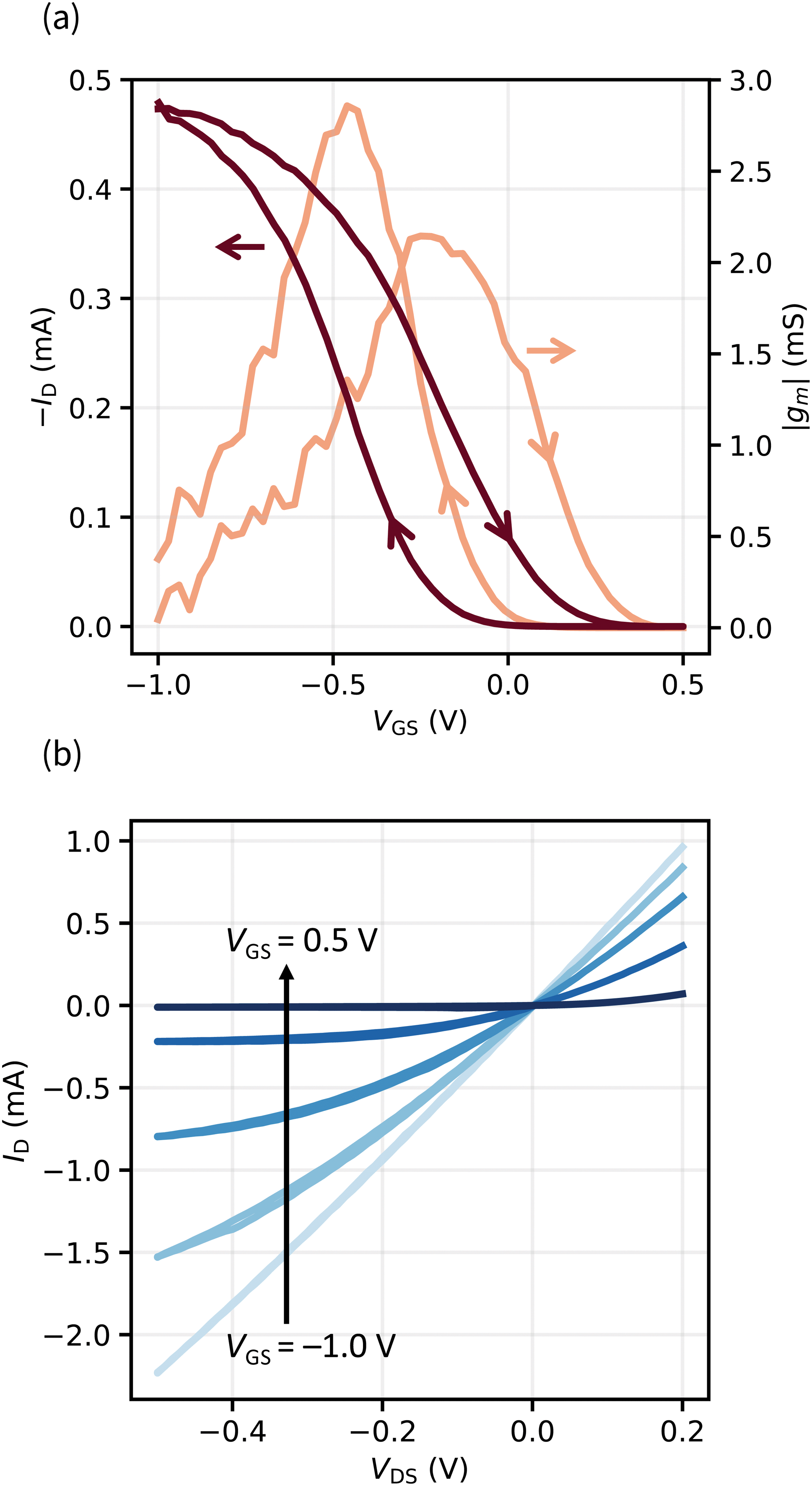 | ||
| Fig. 2 (a) Transfer characteristic and transconductance (|gm|) of an OECT (VDS = −0.1 V). (b) Output characteristics of the same device with VGS = −1.0 V, −0.5 V, −0.25 V, 0 V, and 0.5 V. | ||
We extract the maximum transconductance |gm| with a value of 2.1 mS and the figure of merit μC* with 181 F cm−1 V−1 s−1, which is exceeding most values reported.30 This data was extracted analyzing the switching-off behavior of the device (on → off curve). We observe that from the off-state, upon lowering the gate voltage, the drain current follows a different curve (off → on curve). This hysteretic behavior is very reproducible and will be discussed in detail in the next section.
However, no bias stress effect was observed – an otherwise common, but undesired property of organic transistors.31–33 We conducted stability measurements by recording consecutive transfer curves with no degradation visible (Fig. S4a, ESI†). Additionally, the long-term stability was proven by measuring the device after several days in N2-atmosphere (Fig. S4b, ESI†). In ambient conditions, the threshold voltage shifts to higher values (>0.5 V in 3 days). We attribute this effect to a channel instability rather than to the electrolyte, since its electronic properties remain almost unchanged as proven by impedance spectroscopy in Fig. S5 (ESI†). A resin-based encapsulation solves the problem (Fig. S6, ESI†).
The output characteristics in Fig. 2b indicate that our transistors show saturation behavior and a clear pinch-off point. We investigated OECTs based on a PEDOT:PSS channel because it is the most widely used and studied OMIEC. While the solid electrolyte is expected to be compatible with other hydrophilic semiconducting polymers as well, no gating was observed when tested on the hydrophobic P3HT.
We consider the minimized ionic gate current as the key factor that allows for such good performance of the OECT. As such, we aim to delve deeper into the ion injection mechanism. As mentioned, the patterning reduces leakage paths, hence minimizes the voltage drop across the electrolyte. Consequently, a higher effective voltage drives the device. However, traditional OECTs can show elevated gate currents even when the metal/electrolyte interfaces are passivated, due to lateral movement of ions within the PEDOT:PSS channel. For this reason, we further investigated the interaction of the ionic species of our electrolyte with PEDOT:PSS by producing OECTs gated only with the IL. We find that in N2-atmosphere, the device does not switch off (red curve in Fig. S7a, ESI†). This is coherent with previous findings by Kaphle et al., who attributed it to the excessive size of the ions.34 However, the same system shows a complete switching behavior when a drop of water is added onto it (blue curve in Fig. S7a, ESI†) or when exposed to ambient air (blue curve in Fig. S7b, ESI†). Hence, we conclude that humidity swells the hygroscopic PEDOT:PSS and allows ion movement within the channel. For this particular reason, water is a mandatory component of the solid electrolyte's precursor solution.
A quantification method for hysteresis
As mentioned before, and as visible in the transfer recordings of Fig. 1c and 2a, our solid OECTs are characterized by a large hysteresis. Hysteretic behavior is common in organic transistors35–37 and ubiquitous in OECTs. Its presence is detrimental for IC design but, despite its importance, its analysis is often overlooked. However, it has been shown that if controllable, hysteresis can be harnessed in neuromorphic devices as a short- or long-term memory effect.8,10,38 In this regard, we examine the hysteresis in the transfer curves of our PEDOT:PSS-based solid OECTs and show how its magnitude can be controlled.We found that the hysteresis of our transistors is very reproducible and consistently progressing clockwise (i.e., the absolute value of the current for the on → off curve is higher than the off → on curve). With the intention of utilizing hysteresis as a valid device property, we verified its reliability through recordings taken consecutively as well as on different days (Fig. S4, ESI†). Both the iterative and long-term evaluations proved the hysteresis as persistent in its extent and loop direction. However, we also observe that the strength of the hysteresis is dependent on a number of parameters. To elaborate these, we attempt a systematic investigation in the following, along with proposing a general way to quantify the hysteretic behavior by introducing two parameters θ and ψ.
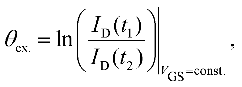
Hysteresis can be defined as the presence of multiple device outputs ID(t1) and ID(t2) to the same input stimulus VGS (see Fig. 3a). The ratio of each pair of outputs can thereby be seen as an indicator of the hysteresis strength at this particular input. By taking the natural logarithm of such ratio,
 | (1) |
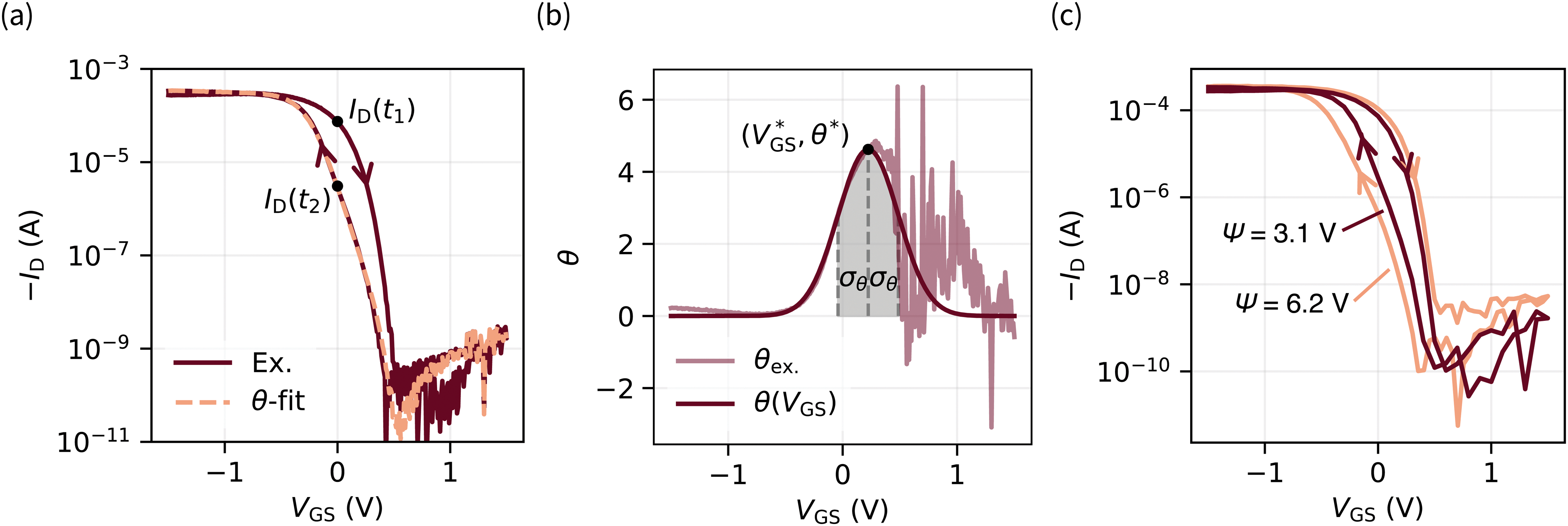 | ||
Fig. 3 (a) Transfer characteristic with labeled points of the on → off (ID(t1)) and off → on (ID(t2)) curve (VDS = −0.1 V). The orange curve was obtained through eqn (3) with fitting parameters for θ(VGS) (eqn (2)) of  θ* = 4.62, and σθ = 0.26 V. (b) Experimental data of eqn (1) (θex.) are approximated by a Gaussian-type expression θ(VGS) (eqn (2)). (c) ψ is defined as the integral of θ(VGS) in boundaries of the scan range (eqn (4)). Two transfer curves are shown with assigned ψ parameters for comparison. A linear plot of this data is provided in Fig. S8 (ESI†). θ* = 4.62, and σθ = 0.26 V. (b) Experimental data of eqn (1) (θex.) are approximated by a Gaussian-type expression θ(VGS) (eqn (2)). (c) ψ is defined as the integral of θ(VGS) in boundaries of the scan range (eqn (4)). Two transfer curves are shown with assigned ψ parameters for comparison. A linear plot of this data is provided in Fig. S8 (ESI†). | ||
As θex. can feature abrupt discontinuities, in particular in the off-state where measurement setups are noisy and the gate current may become dominant, it is useful to find a fitting function. We use a Gaussian-type function θ(VGS) defined as
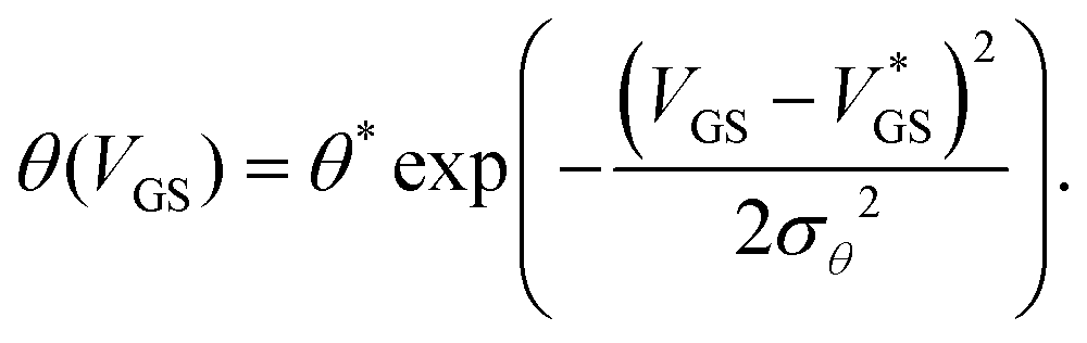 | (2) |
 . We call the gate voltage range, in which the hysteresis mainly takes place, the “hysteresis window”, which is approximately
 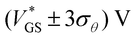 . A visual demonstration of the validity of this approach is given in Fig. 3a, where the θ(VGS)-fit of Fig. 3b was used to model the off → on transfer path by
| ID(t2) = ID(t1)exp(−θ(VGS)). | (3) |
To express the hysteresis in a single quantity, ψ is formulated as the integral of θ(VGS) over the scanned range from VGS,0 to VGS,1:
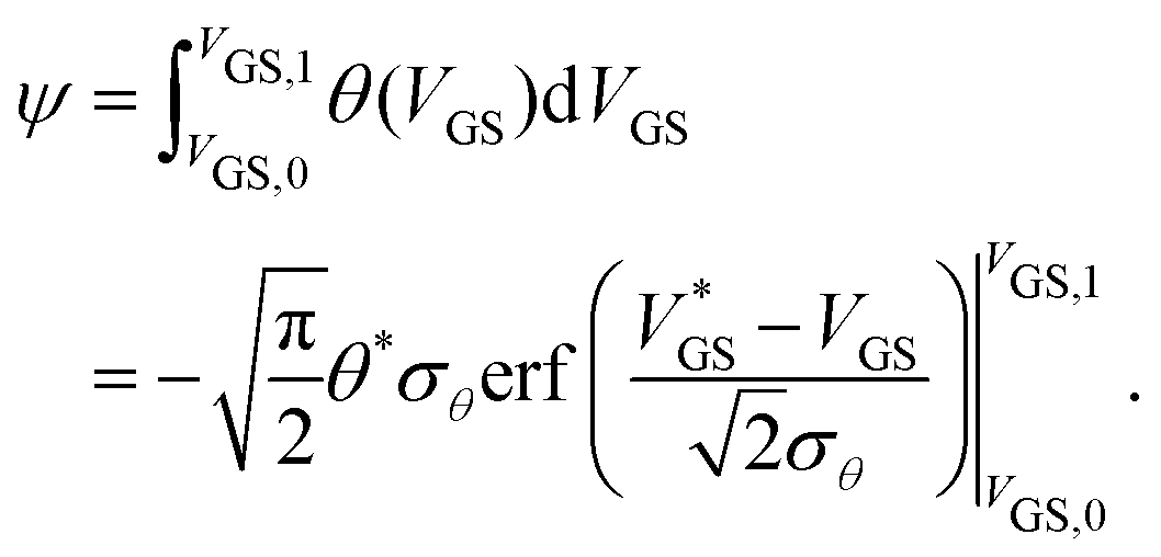 | (4) |
With these equations, we aim to qualitatively describe the hysteretic behavior of OECTs as shown in Fig. 3c. The approach is general and useful for studying device-to-device variability, different materials, and allows to elaborate related dependencies without aiming to reflect precise physical properties through these equations.
Scan range and rate dependence of the hysteresis
With the aim of integrating OECTs into ICs, it is key to gain control over the hysteresis. In this regard, we investigate the hysteresis of the transfer curve varying the scan range i.e., increasing VGS,1 as shown in Fig. 4a.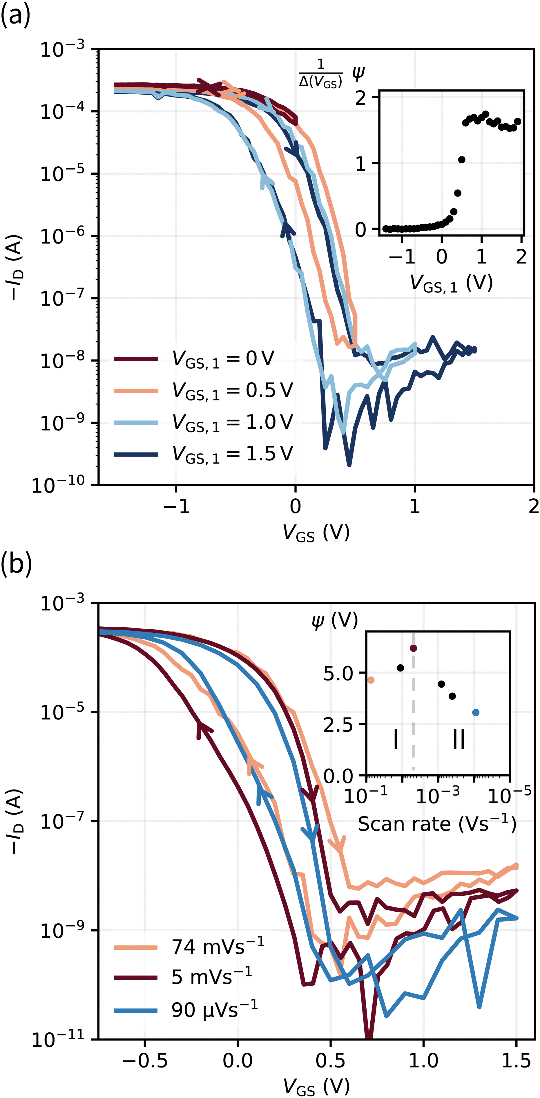 | ||
| Fig. 4 (a) Transfer characteristics of different scan ranges (VGS,0 to VGS,1) revealed a saturation of the hysteresis (VDS = −0.1 V). This behaviour is expressed through ψ parameters in the inset, normalized by Δ(VGS) = VGS,1 − VGS,0. VGS,0 was fixed at −1.5 V. (b) The hysteresis changes with the scan rate, which can be divided into two regimes, as shown in the inset (VDS = −0.1 V). | ||
No hysteresis is observed for VGS,1 < 0 V. Upon exceeding 0 V, dedoping and gating occur, and concurrently the hysteresis increases. The inset of Fig. 4a shows the normalized hysteresis strength ψ, which indicates the strongest increase at VGS,1 ∼ 0.5 V and a saturation for VGS,1 > 0.7 V. This behavior becomes obvious in the light and dark blue transfer curves where the hysteresis window (approximately VGS = −0.5 V to 0.5 V) remains constant upon increasing VGS,1 from 1.0 V to 1.5 V. From these examinations, the hysteresis appears as a reliable feature of our solid OECTs, which can be activated and controlled through the chosen scan range. By switching the device completely, the hysteresis can be driven to its maximum, while an even further increase of the scan range renders it constant.
With regard to the aim of utilizing the hysteresis in circuitry, we investigate the according stability. Similar to memory elements, we examined the retention time by applying and holding a gate bias of 0 V (off → on curve), which yielded a time constant of τRT ∼ 10 min (see Fig. S9, ESI†). It is therefore sufficiently long to consider the two transfer paths as stable within the time periods of transistor switching. Since there is an increase of drain current, the finding implies a decreasing hysteresis for decreasing scan rates. We reviewed this assumption and found a peculiar dependency of the hysteresis strength on the scan rate. When decreasing the scan rate to about 5 mV s−1, the hysteresis strength grows, as a comparison of the red and orange transfer curves in Fig. 4b shows. Only for even slower scans, the expectation of a decrease is fulfilled. This observation is also reflected by ψ in the inset, where two regimes can be identified.
The root of an increasing ψ in the first regime is found in the switching speed of the transistor: the electronic elements used to model the circuit, the electrolyte resistance (RSE) and the channel capacitance CCh, cause a latency of the device to an applied bias, since the capacitor needs to charge through the resistor. The associated time constant is the RC time τRC, which is defined as the product of electrolyte resistance and double layer capacitance. From these considerations, we conclude that the increase in hysteresis of regime I is the result of scan rates exceeding τRC, which accordingly do not switch the device entirely and thus yield a small hysteresis. As the capacitance is directly proportional to the channel thickness, we verify this conclusion by measuring OECTs with various PEDOT:PSS thicknesses at a constant scan rate (Fig. S10, ESI†). Transistors with thicker channel and hence larger τRC indeed show smaller hysteresis at high scan rates (regime I). Conversely, when the scan rate is lower than approximately 5 mV s−1, the device is fully switched and the dependency on the retention time becomes dominant (regime II).
These findings are highly interesting for circuitry, since they demonstrate that, by defining the gate voltage range of operation (e.g.,  ), the transistor can be used as a switch with stable operation on the upper or lower branch of the transfer curve, which enables devices with different threshold voltages. Moreover, the OECTs can be employed as memory devices utilizing the hysteretic behavior, which can be tuned in its extent through the switching speed.
Conclusion
With the aim of achieving dense integration of high-performance OECTs, we design and employ a photopatternable solid electrolyte based on the ionic liquid [EMIM][EtSO4]. We achieve a resolution down to 10 μm and a conductivity of 24 mS cm−1. When employed for PEDOT:PSS-based OECTs, we achieve excellent transistor properties: an outstanding on–off ratio (>105), high μC* (181 F cm−1 V−1 s−1), and a subthreshold swing of 61 mV dec−1, close to the thermodynamic limit. By comparing these results to non-patterned devices, we pinpoint the reason of the improvement to be the minimization of the gate current, which is lowered to the range of nA. Moreover, the patterning eliminates crosstalk between neighboring devices.Finally, we tackle the peculiar and reproducible hysteretic behavior of our OECTs, motivated by the importance that hysteresis has in circuit design and the increasing attention it has been receiving for neuromorphic applications. Even if the question of its origin still needs to be answered, we propose a mathematical model to quantify the hysteresis and we study it under different conditions for demonstrating its utility for advanced applications. These studies conclusively show that the hysteresis possesses a saturated state and that it scales with the scan rate in two regimes, namely the RC time-dominated and the retention time-dominated one.
These achievements are a significant step forward for using OECTs as energy-efficient devices in integrated circuitry, since they provide a framework that allows for dense packaging of high-performance, microscale solid OECTs with standard photolithographic techniques. The accompanying empiric equations are thereby valuable from an engineering perspective, as they allow to systematically adjust and implement the pronounced hysteresis to achieve transistors with multiple transfer paths or neuromorphic features.
Conflicts of interest
There are no conflicts to declare.Acknowledgements
The authors acknowledge the financial support by the European Social Fund (ESF) and the Free State of Saxony in the framework of OrgNanoMorph (SAB proposal no. 100382168) and Re-Learning (SAB proposal no. 100382146). Furthermore, funding by the Deutsche Forschungsgemeinschaft (DFG) within the FlexARTwo project LE 747/52-2 in the DFG Priority Program SPP 1796 is gratefully acknowledged.References
- B. D. Paulsen, K. Tybrandt, E. Stavrinidou and J. Rivnay, Nat. Mater., 2020, 19, 13–26 CrossRef CAS PubMed.
- T. J. Quill, G. LeCroy, A. Melianas, D. Rawlings, Q. Thiburce, R. Sheelamanthula, C. Cheng, Y. Tuchman, S. T. Keene, I. McCulloch, R. A. Segalman, M. L. Chabinyc and A. Salleo, Adv. Funct. Mater., 2021, 2104301 CrossRef CAS.
- J. T. Friedlein, R. R. McLeod and J. Rivnay, Org. Electron., 2018, 63, 398–414 CrossRef CAS.
- J. Rivnay, P. Leleux, M. Ferro, M. Sessolo, A. Williamson, D. A. Koutsouras, D. Khodagholy, M. Ramuz, X. Strakosas, R. M. Owens, C. Benar, J.-M. Badier, C. Bernard and G. G. Malliaras, Sci. Adv., 2015, 1, e1400251 CrossRef PubMed.
- H. Tseng, M. Cucchi, A. Weissbach, K. Leo and H. Kleemann, ACS Appl. Electron. Mater., 2021 Search PubMed.
- M. Ghittorelli, L. Lingstedt, P. Romele, N. I. Craciun, Z. M. Kovács-Vajna, P. W. M. Blom and F. Torricelli, Nat. Commun., 2018, 9, 1441 CrossRef PubMed.
- Y. van de Burgt, E. Lubberman, E. J. Fuller, S. T. Keene, G. C. Faria, S. Agarwal, M. J. Marinella, A. A. Talin and A. Salleo, Nat. Mater., 2017, 16, 414–418 CrossRef CAS PubMed.
- M. Cucchi, H. Kleemann, H. Tseng, G. Ciccone, A. Lee, D. Pohl and K. Leo, Adv. Electron. Mater., 2021, 2100586 CrossRef CAS.
- P. Gkoupidenis, N. Schaefer, B. Garlan and G. G. Malliaras, Adv. Mater., 2015, 27, 7176–7180 CrossRef CAS PubMed.
- X. Ji, B. D. Paulsen, G. K. Chik, R. Wu, Y. Yin, P. K. Chan and J. Rivnay, Nat. Commun., 2021, 12, 1–12 CrossRef PubMed.
- L. Petrauskas, M. Cucchi, C. Grüner, F. Ellinger, K. Leo, C. Matthus and H. Kleemann, Adv. Electron. Mater., 2021, 2100330 CrossRef.
- P. C. Hütter, T. Rothländer, G. Scheipl and B. Stadlober, IEEE Trans. Electron Devices, 2015, 62, 4231–4236 Search PubMed.
- P. A. Ersman, D. Westerberg, D. Tu, M. Nilsson, J. Åhlin, A. Eveborn, A. Lagerlöf, D. Nilsson, M. Sandberg and P. Norberg, et al. , Flexible and Printed Electron., 2017, 2, 045008 CrossRef.
- P. A. Ersman, R. Lassnig, J. Strandberg, D. Tu, V. Keshmiri, R. Forchheimer, S. Fabiano, G. Gustafsson and M. Berggren, Nat. Commun., 2019, 10, 1–9 CrossRef PubMed.
- E. Zeglio and O. Inganäs, Adv. Mater., 2018, 30, 1800941 CrossRef PubMed.
- S. Inal, G. G. Malliaras and J. Rivnay, Nat. Commun., 2017, 8, 1767 CrossRef PubMed.
- M. Cucchi, C. Gruener, L. Petrauskas, P. Steiner, H. Tseng, A. Fischer, B. Penkovsky, C. Matthus, P. Birkholz and H. Kleemann, et al. , Sci. Adv., 2021, 7, eabh0693 CrossRef PubMed.
- A. Melianas, T. Quill, G. LeCroy, Y. Tuchman, H. V. Loo, S. Keene, A. Giovannitti, H. Lee, I. Maria and I. McCulloch, et al. , Sci. Adv., 2020, 6, eabb2958 CrossRef CAS PubMed.
- M. J. Panzer and C. D. Frisbie, J. Am. Chem. Soc., 2007, 129, 6599–6607 CrossRef CAS PubMed.
- D. Khodagholy, V. F. Curto, K. J. Fraser, M. Gurfinkel, R. Byrne, D. Diamond, G. G. Malliaras, F. Benito-Lopez and R. M. Owens, J. Mater. Chem., 2012, 22, 4440–4443 RSC.
- A. Kavanagh, R. Copperwhite, M. Oubaha, J. Owens, C. McDonagh, D. Diamond and R. Byrne, J. Mater. Chem., 2011, 21, 8687–8693 RSC.
- J.-H. Choi, Y. Gu, K. Hong, W. Xie, C. D. Frisbie and T. P. Lodge, ACS Appl. Mater. Interfaces, 2014, 6, 19275–19281 CrossRef CAS PubMed.
- Y. Zhong, G. T. Nguyen, C. Plesse, F. Vidal and E. W. Jager, ACS Appl. Mater. Interfaces, 2018, 10, 21601–21611 CrossRef CAS PubMed.
- N. Tanaka, S. Matsukawa, H. Kurosu and I. Ando, Polymer, 1998, 39, 4703–4706 CrossRef CAS.
- C. Cao, Z.-B. Li, X.-L. Wang, X.-B. Zhao and W.-Q. Han, Front. Energy Res., 2014, 2, 25 Search PubMed.
- T. Ye, L. Li and Y. Zhang, Adv. Funct. Mater., 2020, 30, 2000077 CrossRef CAS.
- H. Dai, G. Zhang, D. Rawach, C. Fu, C. Wang, X. Liu, M. Dubois, C. Lai and S. Sun, Energy Storage Mater., 2021, 34, 320–355 CrossRef.
- V. Bocharova and A. P. Sokolov, Macromolecules, 2020, 53, 4141–4157 CrossRef CAS.
- S. Karan, T. B. Sahu, M. Sahu, Y. Mahipal and R. Agrawal, Ionics, 2017, 23, 2721–2726 CrossRef CAS.
- S. Inal, G. G. Malliaras and J. Rivnay, Nat. Commun., 2017, 8, 1–7 CrossRef CAS PubMed.
- U. Zschieschang, R. T. Weitz, K. Kern and H. Klauk, Appl. Phys. A, 2009, 95, 139–145 CrossRef CAS.
- F. Dollinger, H. Iseke, E. Guo, A. Fischer, H. Kleemann and K. Leo, Adv. Electron. Mater., 2019, 5, 1900576 CrossRef CAS.
- M. P. Hein, A. A. Zakhidov, B. Lüssem, J. Jankowski, M. L. Tietze, M. K. Riede and K. Leo, Appl. Phys. Lett., 2014, 104, 013507 CrossRef.
- V. Kaphle, S. Liu, C.-M. Keum and B. Lüssem, Phys. Status Solidi A, 2018, 215, 1800631 CrossRef.
- M. Egginger, S. Bauer, R. Schwödiauer, H. Neugebauer and N. S. Sariciftci, Monatshefte für Chemie – Chemical Monthly, 2009, 140, 735–750 CrossRef CAS.
- J. Jang, S. H. Kim, S. Nam, D. S. Chung, C. Yang, W. M. Yun, C. E. Park and J. B. Koo, Appl. Phys. Lett., 2008, 92, 143306 CrossRef.
- W. Huang, W. Shi, S. Han and J. Yu, AIP Adv., 2013, 3, 052122 CrossRef.
- J. C. Shank, M. B. Tellekamp, M. J. Wahila, S. Howard, A. S. Weidenbach, B. Zivasatienraj, L. F. Piper and W. A. Doolittle, Sci. Rep., 2018, 8, 12935 CrossRef PubMed.
Footnotes |
| † Electronic supplementary information (ESI) available. See DOI: 10.1039/d1tc04230k |
| ‡ These authors contributed equally to this work. |
| This journal is © The Royal Society of Chemistry 2022 |