DOI:
10.1039/D1TC03133C
(Communication)
J. Mater. Chem. C, 2022,
10, 2556-2561
Molecular design and crystallization process control for thin sheet-shaped organic semiconductor crystals with two-dimensional packing†‡
Received
5th July 2021
, Accepted 31st August 2021
First published on 8th September 2021
Abstract
Sheet-liked organic semiconductor crystals with two-dimensional (2D) packed structures play an essential role in practical applications of high-property optoelectronic devices. Here, we report a practical example in combination with chemical structures and crystallization engineering to construct a balanced 2D network for organic thin sheet-shaped crystals. The introduction of the cyano group enabled the formation of hydrogen bonds, promoting the in-plane 2D network construction both in strength and direction with π⋯π (or C–H⋯π) interactions. Through changing the chamber pressure and growth temperature, we realized a macroscopic morphology adjustment from rods to sheets with the same single crystal structure, ascribed to the relative strength changes of different facet energies. Such a macroscopic dimension control combined with supramolecular chemistry and crystal engineering offers a new perspective for boosting further developments for 2D stacked organic semiconductor crystals.
Two-dimensional (2D) stacked organic semiconductor crystals with thin sheet-liked morphologies have been an ideal material type for optoelectronic device applications.1 Inspired by the development of graphene established by covalent bonds, the sheet-shaped organic crystals are formed by non-covalent bonds.2 Such non-covalent bonds, including the van der Waals force, hydrogen bond, and π⋯π and C–H⋯π interactions, impart the flexibility characteristic to the sheet-liked crystals, facile for the application to electronic devices, mainly for organic field-effect transistors (OFETs). The thin sheet-morphology feature endows the devices with a better interface contact, confining the charges to the 2D plane, generating outstanding charge transport in plane, which are hard to be realized for other bulk-stacked crystals.3 However, currently, just a few compounds have been prepared to 2D stacked thin sheets.4 The connections among the supramolecular engineering, crystal engineering and macroscopic morphologies have so far been dangling with no clues.
The macroscopic morphologies of crystals depend on the crystallization rates of different facets, and the facets with faster crystallization rates will disappear finally.5 The crystallization rates of different facets are pertinent with the intermolecular interactions and facet energies, both of which can be adjusted by changing the chemical structures (supramolecular engineering) and the crystallization process (crystal engineering).6 The 2D packing is to regulate the molecular arrangement along a 2D network under the dominant intermolecular interactions in plane. It should be satisfied to build balanced interactions both in strength and directions between molecular neighbors for the in-plane 2D network, far beyond that along the out-of-plane direction.7 The crystallization rate along the out-of-plane direction is the slowest, thus existent for the final facets. From the supramolecular engineering aspect, on condition of strong π⋯π (or C–H⋯π) interactions, the functional groups at the molecular skeleton can be introduced to form hydrogen bonds along the molecular short axis direction, and manipulate the relative strength of the driving forces during the crystallization process.8 From the crystal engineering aspect, the relative ratios of facet energies can be adjusted by changing the crystal growth conditions, which signifies different dynamic crystallization processes, and performs a vital role in the macroscopic dimension of crystals.9
In recent years, our research group has reported a series of cyano-substituted styrene derivatives and obtained thin-sheet single crystals successfully (Table S1, ESI‡), displaying excellent optoelectronic performances.10 The introduction of a cyano group at a conjugated molecular skeleton enables that the hydrogen bond and π⋯π (or C–H⋯π) interaction in the 2D plane are commensurate in strength and directions, far beyond that of van der Waals force out of the 2D plane. Thus, these two stronger interactions in the 2D network regulate the molecular arrangement to form thin sheets. However, such chemical structures cannot be definitely prepared into thin sheets when the facet energies are changed by the crystallization conditions.11 Up to now, the influence of crystal engineering on macroscopic morphologies has still been ambiguous.
Based on the above-mentioned strategy of supramolecular engineering, we selected (2Z,2′Z)-3,3′-(naphthalene-2,6-diyl)bis(2-(thiophen-3-yl)acrylonitrile) (NBTA) as an example and realized the macroscopic morphology control from rod- to sheet-shaped single crystals without changing the single-crystal structure through accurately adjusting the growth temperature and pressure based on the physical vapor transport (PVT) method. The experimental results indicated that a higher chamber pressure and a lower growth temperature prompted the crystal nucleation density and downsized the crystals, and also restrained the facet growth with a higher growth barrier (van der Waals force direction), boosting the formation of thin sheet crystals. Such instance from molecular design to crystal engineering is promising to promote the development of thin sheet organic single crystals and organic optoelectronics.
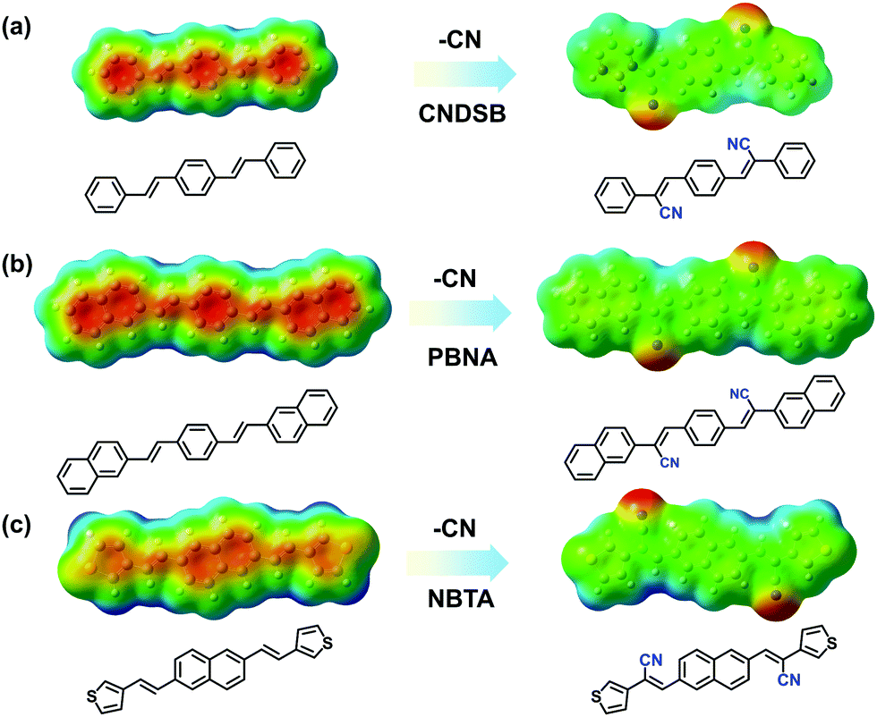
Taking three styrylbenzene derivatives (CNDSB, PBNA and NBTA) as examples, the design principle and features of the chemical structures to form thin-sheet single crystals were interpreted. The single crystal structures implied that the electron-withdrawing cyano group as well as the linear conjugated styrylbenzene skeleton generated strong in-plane hydrogen bonds and π⋯π (or C–H⋯π for PBNA) interactions between the neighbors in three crystals (Fig. S1 and S2, ESI‡), much stronger than those of the van der Waals force. The plots of electrostatic potential (ESP) for the three compounds were employed to characterize the distribution of the π⋯electron cloud density.12 The distribution of the π⋯electron cloud tended to change in the aryl rings before and after the cyano substitution (Fig. 1). The π⋯electron cloud densities of the three model compounds without the cyano substitution were mainly located at the center of the aryl rings. This will give rise to the electrostatic repulsion to some extent, while the molecules are stacked into aggregations,13 harmful for the formation of the 2D network. In contrast, the electron-withdrawing cyano group in substituents depleted the π⋯electron cloud densities in the aryl skeletons, diminishing the electrostatic repulsion of π-stacking, producing the electrostatic attraction between the neighbors, analogous with that of benzene and perfluorobenzene.14 Such electrostatic attraction derived from hydrogen bond could enable the molecule cofacial assembly along the short axis of molecules. Thus, the 2D network interactions could be formed to drive the molecular arrangement. All compounds were prepared to 2D stacked thin sheets successfully.
 |
| | Fig. 1 The changes of ESP distribution for CNDSB (a), PBNA (b) and NBTA (c) compounds with a cyano group substituent. | |
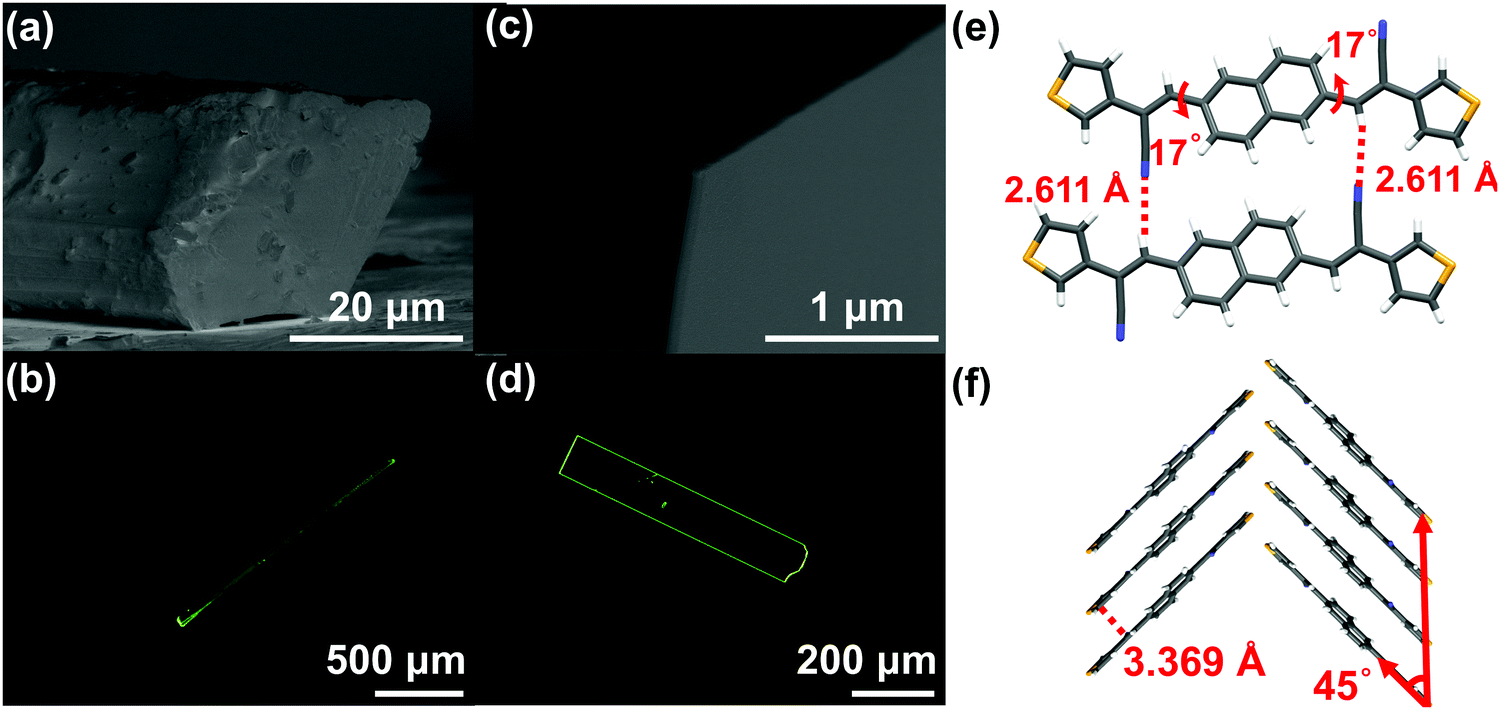
Nevertheless, the above-mentioned characteristics of the molecular structures just satisfied thermodynamic conditions, sufficient, but not necessary for forming sheet single crystals in spite of the obtained 2D stacked morphologies for these three compounds. The crystal morphology is also closely related to dynamic conditions (crystallization process).15 Taking NBTA as an example, we got the well-defined rods and sheets through changing the pressure and the temperature via the PVT method. The detailed growth conditions and crystal morphology information are listed in Table 1. Under the same growth temperature (168 °C) and flow rate (30 mL min−1), the rods were quickly obtained under the lower pressure (∼10−2 Pa) through 3 days, whereas the sheets were slowly deposited under a higher pressure (∼105 Pa) through 6 days. The fluorescence images and cross-section scanning electron microscopes (SEM) showed that the rods were 1.5 to 2.2 mm in the length, with the diameter range of 30 to 50 μm (Fig. 2a and b), while the sheets possessed a flat surface and a well-defined edge with the length, width and thickness of 500 to 650 μm, 125 to 200 μm and 150 to 300 nm (Fig. 2c and d), respectively. The length–width ratios ranged from 3 to 4. Obviously, the sizes of sheets were much smaller than those of the rods. In spite of different macroscopic morphologies, the rods and sheets exhibited the same molecular single crystal structure (Table S2 and Fig. S3, ESI‡). The pressure change was the main factor that resulted in different macroscopic dimensions.
Table 1 The growth conditions and crystal sizes for the two kinds of crystal morphologies
| Morphologies |
Sublimation temperature (°C) |
Growth temperature (°C) |
Flow rate (mL min−1) |
Pressure (Pa) |
Time (d) |
Length (μm) |
Diameter/thickness (nm) |
|
For the rods, 3000–5000 nm represents the diameter of the rods.
For the sheets, 110–330 nm represents the thickness of the sheets.
|
| Rods |
220 |
168 |
30 |
∼10−2 |
3 |
1500–2200 |
3000–5000a |
| Sheets |
240 |
168 |
30 |
∼105 |
6 |
500–650 |
110–330b |
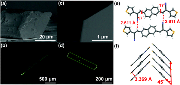 |
| | Fig. 2 The single crystal morphologies and structure information of NBTA crystals: the cross-section SEM (a and c) and fluorescence images (b and d) of rods and sheets; (e and f) the molecular arrangement in a crystal both for the rods and the sheets. | |
The crystallization was composed of a nucleation and a growth process, both of which will impact the final crystal morphology, size and quality. Theoretically, if there is only one nucleus during the whole vapor deposition process, the crystal will grow large enough in a specific space. Therefore, restraining the nucleation density may be an effective method to downsize the crystals for the rods. A dynamic theory of gas could be explained as the following relationships:16
| |  | (1) |
| |  | (2) |
where
λ is the mean free path of gas molecules,
kB is the Boltzmann constant,
T is the deposition temperature,
P is the chamber pressure,
d is the effective diameter,
Z is the collision frequency, and
ν is the movement rate of gas molecules. The higher chamber pressure
P can limit the mean free path
λ accompanied with increased collision frequency
Z, which leads to more active sites and higher nucleation density with a decreased crystal size. Therefore, according to these two relationships, reducing the growth temperature
T or raising the chamber pressure
P will increase the nucleation density, beneficial to acquire smaller-size sheet-shaped crystals.
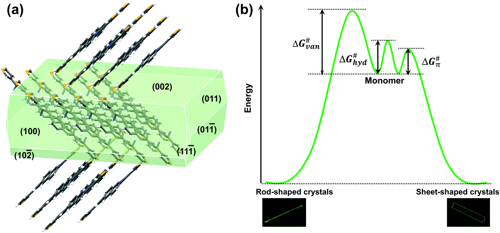
For the crystal growth process, the intermolecular interactions of the NBTA molecules comprised hydrogen bond (C–H⋯N), π⋯π interaction and weak van der Waals force (Fig. 2e and f), which could be estimated by morphology simulation. Because of the lack of external solvent-induced interactions for the PVT method, the crystallization model for nucleation and growth process could be simplified, which will be advantageous to further explore the mechanism of crystallization.17 The attachment energies with various crystal facets and crystal morphology were simulated by the growth morphology method. The attachment energy is defined as released energy with a new atom/molecule adsorbed on the facet. The attachment rule could be expressed as the following equation:8,18
| | | Rrel(hkl) = A*Eattach(hkl) | (3) |
where
Rrel(hkl) is the growth rate of (
hkl) facet,
A is the actual area of (
hkl) facet, and
Eattach(hkl) is the attachment energy of (
hkl) facet. According to this equation, the growth rate of a facet is proportional to the corresponding attachment energy. The facets with a lower attachment energy signify higher growth barrier and slower growth rate, present for the final facets with a smaller Miller index (
Table 2).
5,19 As shown in
Fig. 3a, the simulated crystal facets of (100) and (10
![[2 with combining macron]](https://www.rsc.org/images/entities/char_0032_0304.gif)
) belong to the C–H⋯N direction, while the (011) facet pertains to the π⋯π direction and (002) facet presents a weak van der Waals force direction. The area proportion of the (11
![[1 with combining macron]](https://www.rsc.org/images/entities/char_0031_0304.gif)
) facet is so small that it could be ignored. The growth rates of different facets followed the order:
Rrel(11) >
Rrel(011) >
Rrel(10) >
Rrel(100) >
Rrel(002), and the order of growth barriers for the facets was reversed. Among all growth rates of facets along three directions, the growth rate along the π⋯π direction was the fastest, 3.3 times faster than that along the van der Waals force direction, while the growth rate along the hydrogen bond direction was 1.9 times faster than that along the van der Waals force direction. Thus, the growth barrier along the van der Waals force direction was the highest, and the lowest for that along the π⋯π direction (
Fig. 3b). The rods and sheets displayed the same melting point of 285 °C (Fig. S4, ESI
‡), implying the same energy and stability. As the temperature was constant, the lower pressure led to a smaller number of gas molecules to be condensed and crystallized. Besides, the molecular transitional energy was determined by the temperature according to the following equation:
20| |  | (4) |
where

is the transitional energy per molecule. When the growth temperature was unchanged, the total transitional energy was constant for all the gas molecules in the chamber. A smaller number of molecules with higher transitional energy per molecule could get over a higher growth barrier along the van der Waals force direction to aggregate and crystallize. The lower chamber pressure gave rise to all the facet growth with poor selectivity of the facet growth, helpful for forming rods, whereas a higher pressure restrained the facet growth with a higher barrier along the van der Waals force direction, beneficial to the facet growth along the hydrogen bond and π⋯π directions to form 2D packed sheets.
Table 2 The calculated attachment energies of the final facets for the simulated NBTA crystal morphology
| (hkl) |
E
attach (Total) (kcal mol−1) |
d
(hkl) (Å) |
Total facet area (%) |
| (002) |
−16.36 |
14.02 |
61.92 |
| (100) |
−47.13 |
6.93 |
18.49 |
| (10) |
−48.52 |
6.43 |
4.26 |
| (011) |
−70.81 |
4.73 |
15.02 |
| (11) |
−84.59 |
3.93 |
0.30 |
 |
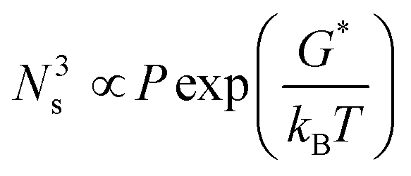
| | Fig. 3 The simulated crystal morphology and the schematic of the crystallization process: (a) the simulated morphology and corresponding facets based on the NBTA single crystal through the “growth morphology” method; (b) the different crystallization processes of rod- and sheet-shaped crystals from monomer to crystal states. (Note: the ΔG≠van, ΔG≠hyd and ΔG≠π represents the growth barriers along the van der Waals force direction, hydrogen bond and π⋯π directions, respectively). | |
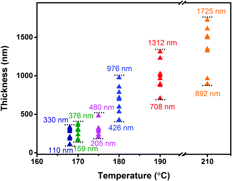
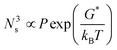
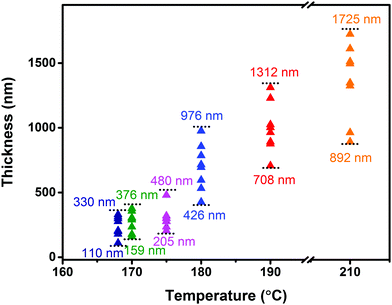
In order to further investigate the influence of the growth temperature on the crystal morphology, we gradually changed the growth temperature under isobaric conditions (∼105 Pa) to grow crystals. The obtained sheet-shaped crystals showed temperature-dependent thickness with an unchanged length to width ratio (3–4). As the growth temperature was increased from 168 °C to 210 °C under the sublimation temperature of 240 °C, the crystal thickness increased from 200 nm to 1700 nm from the surface profiler (Fig. 4). Irrespective of whether the crystals were thin or thick, they exhibited a smooth and flat surface without any steps (Fig. S5, ESI‡). The crystal nucleation density was determined by the following relationship:16,21
| |  | (5) |
where
Ns is the nucleation density,
P is the partial pressure of the precursor molecule, and
G* is the nucleation barrier. With the growth temperature increased, the crystal nucleation density decreased and molecular transition energy also increased. The supply of thermal energy was sufficient enough to overcome the growth barrier of facets along the van der Waals force direction with a higher growth barrier, promoting the growth rates of facets along the van der Waals force direction. The growth rates of facets along the hydrogen bond and π⋯π direction suffered from little impact, which was a slow crystallization process.
 |
| | Fig. 4 The thickness of the crystals under different growth temperatures tested from a surface profiler. | |
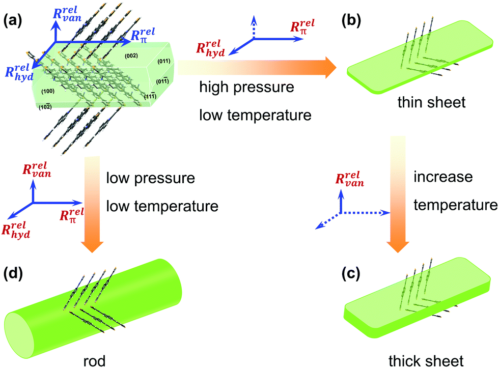
Compared to the influence of the pressure on the crystal morphology, the temperature increased by 0.25-fold from 168 °C to 210 °C, while the pressure increased by 107-folds. The pressure change had a greater impact on the crystal morphology, thus generating larger millimeter-scale rods compared to micrometer-sized sheets. Fig. 5 displays a possible evolution process of the facet growth along the three main directions under different growth conditions. Under the optimized crystal growth conditions, the high-quality thin sheets displayed mobilities in organic single field-effect transistors, where μe = 0.54 cm2 V−1 s−1 and μh = 0.004 cm2 V−1 s−1 (Fig. S6 and S7, ESI‡), respectively. The high-quality thin-sheet single crystals could offer a new pathway for further fabricating desired-morphology organic crystals and constructing excellent optoelectronics.
 |
| | Fig. 5 The different facet growth processes of the NBTA crystal under different chamber pressures and growth temperatures: (a) the formed crystal nuclear; (b) the obtained thin sheets at high pressure and low temperature from the formed crystal nuclear (a); (c) the thick sheets via increasing temperature from (b); (d) the obtained rods at low pressure and low temperature from the formed crystal nuclear (a). (Note: the Rrelvan, Rrelhyd and Rrelπ represent the growth rates along van der Waals force, hydrogen bond and π⋯π direction directions, respectively; the full line means main growth direction, and the dashed line implies the suppressed growth direction). | |
Conclusions
In summary, we presented an instance to fabricate 2D packed organic thin-sheet single crystals from supramolecular chemistry to crystal engineering. The hydrogen bond derived from the electron-withdrawing cyano group along the short axis of molecules and the π⋯π interaction from linear conjugated molecular skeletons constituted a 2D network in plane, and regulated the molecular arrangement to form 2D packed thin sheets. Based on these thermodynamic conditions, the macroscopic morphology regulation of NBTA crystals was realized from rods to sheets by adjusting the dynamic conditions (chamber pressure and growth temperature) based on the PVT method. The experimental results demonstrated that the higher chamber pressure and the lower growth temperature not only augmented the crystal nucleation density, but also were conducive to the facet growth with lower growth barriers (along the π⋯π and hydrogen bond directions), which could downsize the crystals to obtain thin sheets. Such macroscopic morphology control and analysis can provide a model for engineering sheet-shaped crystals with high quality to construct organic optoelectronic devices.
Conflicts of interest
There are no conflicts to declare.
Acknowledgements
This work was financially supported by the National Key R&D Program of China (2020YFA0714604), the Natural Science Foundation of China (91833304, 21973081 and 51521002), the Basic and Applied Basic Research Major Program of Guangdong Province (No. 2019B030302007), the Research and Development Funds for Science and Technology Program of Guangzhou (No. 202007020004), the Natural Science Foundation of Guangdong Province (2019B121205002) and the Guangdong Provincial Key Laboratory of Luminescence from Molecular Aggregates (2019B030301003).
Notes and references
-
(a) L. Zhang, M. M. Hasan, Y. Tang, A. R. Khan, H. Yan, T. Yildirim, X. Sun, J. Zhang, J. Zhu, Y. Zhang and Y. Lu, Mater. Today, 2021 DOI:10.1016/j.mattod.2021.02.021;
(b) W. Wang, B. Lu, W. Deng, X. Zhang, Z. Lu, D. Wu, J. Jie and X. Zhang, Nano Res., 2020, 13, 2478–2484 CrossRef.
-
(a) X. Zhuang, Y. Mai, D. Wu, F. Zhang and X. Feng, Adv. Mater., 2015, 27, 403–427 CrossRef PubMed;
(b) X. Li, L. Tao, Z. Chen, H. Fang, X. Li, X. Wang, J.-B. Xu and H. Zhu, Appl. Phys. Rev., 2017, 4, 021306 CrossRef;
(c) D. Goyal, S. K. Mittal, A. Choudhary and R. K. Dang, Mater. Today: Proc., 2021, 43, 203–208 Search PubMed.
- H. Li, Y. Li, H. Li and J.-L. Brédas, Adv. Funct. Mater., 2017, 27, 1605715 CrossRef.
-
(a) Y.-L. Shi, M.-P. Zhuo, X.-D. Wang and L.-S. Liao, ACS Appl. Nano Mater., 2020, 3, 1080–1097 CrossRef;
(b) M.-P. Zhuo, Y.-C. Tao, X.-D. Wang, Y. Wu, S. Chen, L.-S. Liao and L. Jiang, Angew. Chem., Int. Ed., 2018, 130, 11470–11474 CrossRef;
(c) H. Zhao, Y. Zhao, Y. Song, M. Zhou, W. Lv, L. Tao, Y. Feng, B. Song, Y. Ma, J. Zhang, J. Xiao, Y. Wang, D.-H. Lien, M. Amani, H. Kim, X. Chen, Z. Wu, Z. Ni, P. Wang, Y. Shi, H. Ma, X. Zhang, J.-B. Xu, A. Troisi, A. Javey and X. Wang, Nat. Commun., 2019, 10, 1–9 CrossRef.
-
J. W. Mullin, Crystallization, Butterworth Heinemann, Oxford, 1992 Search PubMed.
- M. A. Lovette, A. R. Browning, D. W. Griffin, J. P. Sizemore, R. C. Snyder and M. F. Doherty, Ind. Eng. Chem. Res., 2008, 47, 9812–9833 CrossRef.
- B. Hu and P. Wu, Nano Res., 2020, 13, 868–874 CrossRef.
- S. K. Park, J. H. Kim and S. Y. Park, Adv. Mater., 2018, 30, 1704759 CrossRef.
- J. E. Park, M. Son, M. Hong, G. Lee and H. C. Choi, Angew. Chem., Int. Ed., 2012, 51, 6383–6388 CrossRef.
-
(a) Y. Wan, J. Deng, C. Gu and Y. Ma, J. Mater. Chem. A, 2021, 9, 2120–2125 RSC;
(b) Y. Wan, J. Deng, W. Wu, J. Zhou, Q. Niu, H. Li, H. Yu, C. Gu and Y. Ma, ACS Appl. Mater. Interfaces, 2020, 12, 43976–43983 CrossRef;
(c) L. Liu, C. Cai, Z. Zhang, S. Zhang, J. Deng, B. Yang, C. Gu and Y. Ma, ACS Mater. Lett., 2021, 3, 428–432 CrossRef;
(d) H. Wang, F. Li, I. Ravia, B. Gao, Y. Li, V. Medvedev, H. Sun, N. Tessler and Y. Ma, Adv. Funct. Mater., 2011, 21, 3770–3777 CrossRef;
(e) X. Li, N. Gao, Y. Xu, F. Li and Y. Ma, Appl. Phys. Lett., 2012, 101, 063301 CrossRef;
(f) X. Li, Y. Xu, F. Li and Y. Ma, Org. Electron., 2012, 13, 762–766 CrossRef;
(g) J. Deng, J. Tang, Y. Xu, L. Liu, Y. Wang, Z. Xie and Y. Ma, Phys. Chem. Chem. Phys., 2015, 17, 3421–3425 RSC;
(h) J. Deng, Y. Xu, L. Liu, C. Feng, J. Tang, Y. Gao, Y. Wang, B. Yang, P. Lu, W. Yang and Y. Ma, Chem. Commun., 2016, 52, 2370–2373 RSC;
(i) Y. Xu, Z. Xie, H. Zhang, F. Shen and Y. Ma, CrystEngComm, 2016, 18, 6824–6829 RSC;
(j) Y. Xu, K. Wang, Y. Zhang, Z. Xie, B. Zou and Y. Ma, J. Mater. Chem. C, 2016, 4, 1257–1262 RSC.
- Y. Xu, H. Zhang, F. Li, F. Shen, H. Wang, X. Li, Y. Yu and Y. Ma, J. Mater. Chem., 2012, 22, 1592 RSC.
- S. E. Wheeler, J. Am. Chem. Soc., 2011, 133, 10262–10274 CrossRef PubMed.
- J.-H. Dou, Y.-Q. Zheng, Z.-F. Yao, T. Lei, X. Shen, X.-Y. Luo, Z.-A. Yu, S.-D. Zhang, G. Han, Z. Wang, Y. Yi, J.-Y. Wang and J. Pei, Adv. Mater., 2015, 27, 8051–8055 CrossRef CAS.
- J. H. Wilhams, Acc. Chem. Res., 1993, 26, 593–598 CrossRef.
-
(a) G. R. Desiraju, Nat. Mater., 2002, 1, 77–79 CrossRef CAS PubMed;
(b) S.-M. Lee, S.-N. Cho and J. Cheon, Adv. Mater., 2003, 15, 441–444 CrossRef CAS.
- X. Tong, K. Liu, M. Zeng and L. Fu, InfoMat, 2019, 1, 460–478 CrossRef CAS.
- C. Wang, H. Dong, L. Jiang and W. Hu, Chem. Soc. Rev., 2018, 47, 422–500 RSC.
- L. Kang, H. Fu, X. Cao, Q. Shi and J. Yao, J. Am. Chem. Soc., 2011, 133, 1895–1901 CrossRef CAS.
- H. Liu, X. Cao, Y. Wu, Q. Liao, Á. J. Jiménez, F. Würthner and H. Fu, Chem. Commun., 2014, 50, 4620–4623 RSC.
-
X. Fu, W. Shen, T. Yao and W. Hou, Physical Chemistry, Higher Education Press, Beijing, 2005 Search PubMed.
- H. Kim, C. Mattevi, M. R. Calvo, J. C. Oberg, L. Artiglia, S. Agnoli, C. F. Hirjibehedin, M. Chhowalla and E. Saiz, ACS Nano, 2012, 6, 3614–3623 CrossRef CAS.
Footnotes |
| † Dedicated to Professor Daoben Zhu on the occasion of his 80th birthday. |
| ‡ Electronic supplementary information (ESI) available: Theoretical calculation, single-crystal structural information, crystal growth and device performance. CCDC 2094453 and 2094241. For ESI and crystallographic data in CIF or other electronic format see DOI: 10.1039/d1tc03133c |
| § These authors contributed equally to this work. |
|
| This journal is © The Royal Society of Chemistry 2022 |
Click here to see how this site uses Cookies. View our privacy policy here. 
 a and
Yuguang
Ma
a and
Yuguang
Ma

 is the transitional energy per molecule. When the growth temperature was unchanged, the total transitional energy was constant for all the gas molecules in the chamber. A smaller number of molecules with higher transitional energy per molecule could get over a higher growth barrier along the van der Waals force direction to aggregate and crystallize. The lower chamber pressure gave rise to all the facet growth with poor selectivity of the facet growth, helpful for forming rods, whereas a higher pressure restrained the facet growth with a higher barrier along the van der Waals force direction, beneficial to the facet growth along the hydrogen bond and π⋯π directions to form 2D packed sheets.