
Controllable growth of centimeter-scale 2D crystalline conjugated polymers for photonic synaptic transistors†
Qing
Zhang
 a,
Xin
Ye
b,
Yue
Zheng
c,
Yongshuai
Wang
d,
Lin
Li
*e,
Zhansheng
Gao
f,
Jinxiong
Wu
f,
Huanli
Dong
d,
Dechao
Geng
*g and
Wenping
Hu
*ag
a,
Xin
Ye
b,
Yue
Zheng
c,
Yongshuai
Wang
d,
Lin
Li
*e,
Zhansheng
Gao
f,
Jinxiong
Wu
f,
Huanli
Dong
d,
Dechao
Geng
*g and
Wenping
Hu
*ag
aJoint School of National niversity of Singapore and Tianjin University, International Campus of Tianjin University, Fuzhou 350207, China. E-mail: huwp@tju.edu.cn
bDepartment of Chemistry, National University of Singapore, Singapore 117543, Singapore
cDepartment of Physics, National University of Singapore, 2 Science Drive 3, 117542, Singapore
dBeijing National Laboratory for Molecular Sciences, Key Laboratory of Organic Solids, Institute of Chemistry, Chinese Academy of Sciences, Beijing 100190, China
eInstitute of Molecular Plus, Tianjin University, Tianjin 300072, China. E-mail: linli2020@tju.edu.cn
fTianjin Key Lab for Rare Earth Materials and Applications, Center for Rare Earth and Inorganic Functional Materials, School of Materials Science and Engineering, National Institute for Advanced Materials, Nankai University, Tianjin 300350, China
gDepartment of Chemistry, Tianjin University & Collaborative Innovation Center of Chemical Science and Engineering (Tianjin), Tianjin 300072, China. E-mail: gengdechao_1987@tju.edu.cn
First published on 3rd August 2021
Abstract
Two-dimensional (2D) crystals of conjugated polymers (2DCCPs) have attracted significant attention in the past few decades due to their superior and intriguing optoelectronic properties. With the increase in brain-inspired neuromorphic computing, 2DCCPs have also been employed in the construction of synaptic devices because they offer clear advantages of easy integration, high stability, long–range order and no biological rejection. However, pursuing controllable strategies to obtain high-quality and large-scale 2DCCPs remains a challenge on account of their intrinsic complex structures. Herein, we present a universal methodology to grow centimeter-scale 2DCCPs in a controlled manner within minutes by selecting an appropriate growth-assisting solvent and surfactant. The thickness of the as-produced 2DCCPs was down to two molecular layers. The photonic synaptic transistors based on the as-grown 2DCCPs could perform typical synaptic functions, including short-term plasticity, paired-pulse facilitation, long-term plasticity and spike intensity-dependent plasticity. The transistor was also proven to have potential application as a high-pass filter. This methodology shows great potential to be expanded to many other polymer systems and opens new pathways for large-area integrated wireless communication systems and artificial visual systems.
1. Introduction
Currently, von Neumann-based computation faces serious challenges in unstructured problems due to its physical separation of memory and processor.1 On the contrary, neuromorphic computation shows great potential to address unstructured issues in addition to the advantages of massive parallelism and flexible adaptive capability. Mimicking the functions of the human brain through electronic devices based on semiconducting materials has attracted significant attention in the past few decades. In the biological neural network, synapses play a significant role in the transmission of signals.2,3 Currently, diverse progressive artificial synapses have been developed, such as ferroelectric polarization-governed synaptic devices4 and crossbar memristors based on vertical organic nanocrystal arrays.5 However, the bottleneck of large-scale integration is still the main obstacle in the realization of their commercial application.Two-dimensional (2D) crystals of conjugated polymers (2DCCPs), which have the unique advantages of long–range order, no biological rejection, scalability and flexibility, can serve as ideal materials to solve the challenge of large-scale integration.6 Besides, 2D materials are beneficial to solve the short-channel effect.4,7 However, only a few efficient preparation methods and reasonable mechanisms for the growth of 2DCCPs have been reported due to the intricate structures of their polymer chains. Currently, the reported methodologies, including close-jar evaporation8 and off-site spin-coating9 cannot overcome the predicament of uneven growth, and thus are not beneficial for integration. Over the past decade, researchers have made a breakthrough in the controllable growth of 2D crystals of organic semiconductors on the surface of water, which is mainly due to the following reasons: (1) the appropriate ductility of water surface enables an even spread of solution. (2) Dynamic assembly can be implemented under the assistance of the fluidity of water. (3) A crystalline thin film with a controllable area can be achieved through epitaxial growth or by the use of multiple surfactants. Xu et al. were the first to develop a solution epitaxy method for the self-assembly of 2D crystals of organic semiconductor on the surface of water by virtue of π–π molecular interactions.10 Subsequently, Wang et al. introduced surfactants to enhance the surface spreading and further increase the area of 2D crystals.11 These results demonstrated the prospect of preparing 2D crystals at the water/air interface. However, in contrast to the above-mentioned 2D crystals of organic semiconductors, the molecular interactions in conjugated polymers are much more complicated, leading to countless conformations.12,13 Actually, the self-assembly of polymer chains cannot occur spontaneously without the assistance of external forces, i.e., solvents14 and chemical reactions.15,16 In addition, it takes one day or even several days for conventional solution epitaxy to obtain products, thus leading to low efficiency.
Herein, a space-confined drop-casting method is proposed for the first time to adapt the growth of 2DCCPs. This method makes full use of the advantages of a suitable solvent and surfactant. The use of a suitable solvent significantly enhances the solubility of conjugated polymers, and meanwhile determines the evaporate rate, which is further directly related to the shear force. The appropriate contact angle between water and the solvent is ascribed to the surfactant, dramatically increasing the spreading of the solvent. Thus, the synergistic effect induced by a suitable solvent and surfactant is beneficial for the efficient preparation of high-quality large-area 2DCCPs.
2. Results and discussion
2.1. Assembly routes
In this work, tetrabutylammonium bromide (TBAB) was chosen to be added to deionized water, and the reason why TBAB was chosen as the surfactant can be found in our previous work.11 Conjugated polymers were dissolved in chloroform and then gently dropped onto the surface of water. Chloroform provided clear advantages of similar solubility parameter to that of the conjugated polymers and low boiling point, leading to a high evaporation rate. More detailed information on the choice of chloroform is presented in Note S1 and Table S1 (ESI†).A schematic of the space-confined drop-casting method is shown in Fig. 1a. With the assistance of TBAB, enhanced spreading was achieved, and as the chloroform evaporated rapidly, a membrane was formed on the entire surface of the water within several minutes. Taking poly(3-hexylthiophene-2,5-diyl) (P3HT) as an example, direct self-assembly on the surface of water could be observed with the naked eyes at room temperature with time from 0 s to 240 s (Fig. 1b and Movie in the ESI†). The shear force generated by the evaporation of the low boiling point chloroform drove the ordered growth of the conjugated polymer chains, where the conjugated polymer chains tended to aggregate to reduce the hydrophobic effect.17
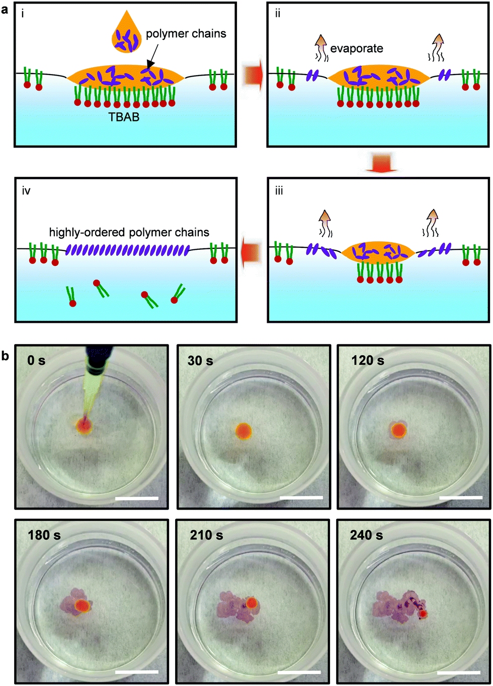 | ||
| Fig. 1 Principle and process for the formation of 2DCCPs via space-confined drop-casting, taking P3HT as an example. (a) Schematic diagram of space-confined drop-casting method. (b) Growth process of 2DCCPs on the surface of water observed with the naked eyes at different times. Scale bar: 2 cm. | ||
2.2. Quality characterization
This space-confined drop-casting method was proven to be general for the preparation of 2DCCPs. Optical microscopy, high-resolution transmission electron microscopy (HR-TEM) and selected-area diffraction (SAED) were employed to analyze the structures of the 2D crystals produced by the space-confined drop-casting method. Three typical conjugated polymers were demonstrated, i.e., P3HT, poly(2,5-bis(3-hexadecylthiophen-2-yl)thieno[3,2-b]thiophene) (PBTTT-C16) and poly[2,5-bis(3-tetradecylthiophen-2-yl)thieno[3,2-b]thiophene] (PBTTT-C14), and their chemical structures are presented in the inset of Fig. 2a, d and g, respectively. The crystals were free-standing and could be easily transferred onto the surface of silicon/silicon dioxide (Si/SiO2) wafers or TEM copper grids. The lateral size of the crystals reached the micrometer level, and their microscopic images are shown in Fig. 2a, d and g, respectively. HR-TEM was employed to further confirm the π–π stacking between the polymer chains. The HR-TEM image of the P3HT crystal is shown in Fig. 2b. By averaging the spacing between multiple lattice fringes, the spacing between adjacent lattice fringes was calculated to be 3.76 Å, which is identical to the d-spacing of the (010) plane along the π–π stacking direction of P3HT chains.18,19 The SAED pattern shown in Fig. 2c also exhibits a distance of 3.70 Å, which is consistent with the corresponding HR-TEM pattern. The HR-TEM pattern and SAED pattern of the PBTTT-C16 crystal are shown in Fig. 2e and f, respectively. The d-spacing of the (010) plane was calculated to be 3.72 Å, which also corresponds to the distance of π–π stacking.20 The periodic scattered dots in the SAED pattern indicate the high crystallinity of the as-prepared sample. Meanwhile, the distance between adjacent fringes calculated from Fig. 2h is 3.61 Å, corresponding to the d-spacing of the (010) plane in the PBTTT-C14 crystals. The bright dots group in the SAED pattern also demonstrate significant crystallization.21 The self-shearing force generated from the evaporation of chloroform was proven to be effective for the preparation of 2DCCPs.22 Thus, this general method is promising to afford a platform to investigate the relationship between properties and structures of 2DCCPs.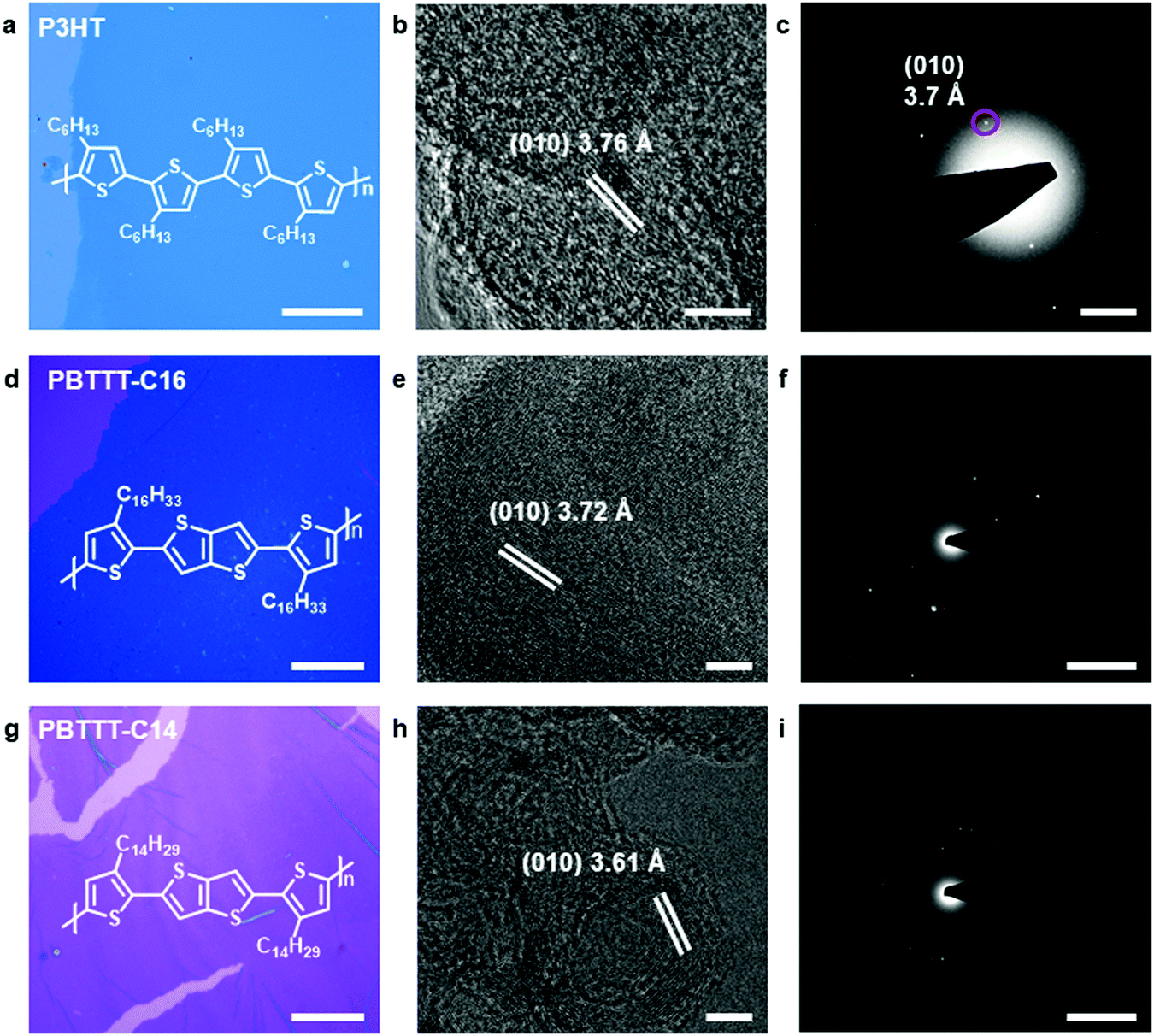 | ||
| Fig. 2 Characterization of 2DCCPs. P3HT, PBTTT-C16 and PBTTT-C14 were used to demonstrate the universality of the space-confined drop-casting method. (a, d and g) Microscopic images of the three 2DCCPs, respectively. The inset shows the chemical structures of the conjugated polymers. Scale bar: 50 μm. (b, e and h) HR-TEM images of the three 2DCCPs, respectively. Scale bar: 5 nm. (c, f and i) Corresponding SAED patterns of the three 2DCCPs, respectively. Scale bar: 2 nm−1, 5 nm−1, and 5 nm−1, respectively. | ||
More detailed characterization of the P3HT crystals is summarized in Fig. 3. Fig. 3a demonstrates a centimeter-scale area of the obtained P3HT crystal and the TEM image in Fig. 3b exhibits the microscopic continuous membrane structure. Raman measurements were also performed on the films (Fig. 3c). The characteristic peaks of P3HT at 1376 cm−1 and 1447 cm−1 were clearly identified,23 while the peak at 519 cm−1 is attributed to the silicon substrate.24–26 The Raman signal for the P3HT crystal showed a very high signal-to-noise ratio and narrow peak width, whose full width at half maxima (FWHM) is less than 50 cm−1, demonstrating compact stacking towards high crystallinity. A flat and uniform surface was visualized by the Raman mapping characterization of the peaks located at 1447 cm−1 and 519 cm−1 (Fig. 3e and f, respectively), and the selected mapping area is shown in Fig. 3d. Besides the folds of the 2D crystal, the intensities of the Raman signals from different regions in the P3HT crystal were all consistent, which proves its good homogeneity.
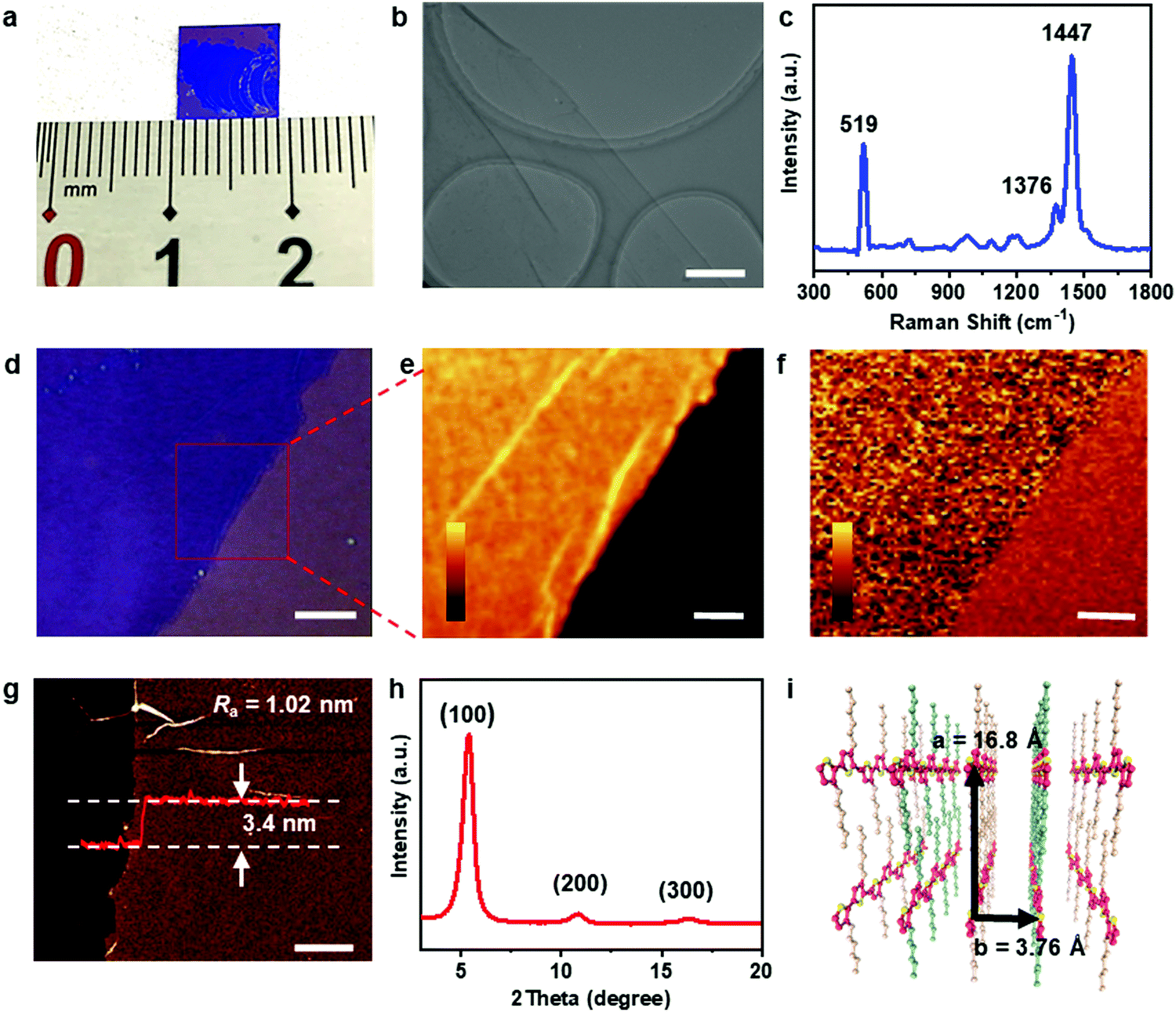 | ||
| Fig. 3 Characterization of the centimeter-scale P3HT crystals. (a) Macroscopic image of the obtained P3HT crystal. (b) TEM image of the film. Scale bar: 1 μm. (c) Sharp and narrow Raman spectrum of the P3HT crystal. (d) Microscopic image of the film and the red frame in the image is the Raman mapping region. Scale bar: 10 μm. (e) Mapping result of the 1447 cm−1 peak, corresponding to the uniform existence of P3HT. Scale bar: 3 μm. (f) Mapping result of the 519 cm−1 peak, corresponding to the silicon substrate. Scale bar: 3 μm. (g) AFM image of the film, where the thickness of the film is 3.4 nm. Ra = 1.02 nm. Scale bar: 2 nm. (h) XRD profile of the crystal. (i) Expected packing mode of the molecular chains on the substrate, where the a axis is defined as the direction along the side alkyl chains and the b axis is defined as the direction along the π–π packing. | ||
The structure of the P3HT crystal was further characterized. Atomic force microscopy (AFM) characterization showed that the surface of the films was smooth with Ra = 1.02 nm, indicating the good quality of the sample. The thickness of the P3HT film was measured to be 3.4 nm, corresponding to two molecular layers (Fig. 3g).7 The out-of-plane X-ray diffraction (XRD) profile of the P3HT crystal transferred onto the Si/SiO2 substrate showed a series of (h00) reflections, as shown in Fig. 3h. The diffraction peaks located at 2θ = 5.25°, 10.50° and 15.70° are assigned to the (100), (200) and (300) planes, respectively. The d-spacing calculated from the (100) plane is 16.8 Å, representing the interlamellar spacing along the direction of the alkyl side chains. According to the above-mentioned HR-TEM and SAED data, the polymer chains in the P3HT crystals are predicted to lie rather than stand on the substrate. Thus, an edge-on arrangement of the polymer backbones on the substrate is proposed,27 as shown in Fig. 3i.
2.3. Optoelectrical properties
As predicted, the crystallization of the conjugated polymers would induce an enhancement in their electronic properties.28 Therefore, field-effect transistors (FETs) based on P3HT crystals were constructed to investigate their electronic properties. The detailed fabrication process and the scanning electronic microscopy (SEM) image of the device is shown in Fig. S1 and S2 (ESI†), respectively. Fig. S3a (ESI†) shows a representative transfer curve of the device and Fig. S3b (ESI†) shows representative output curves. Based on 23 devices randomly selected from different batches, the distribution of their hole mobilities was obtained (Fig. S3c, ESI†). The statistical results showed that the highest mobility of our P3HT crystal can reach 0.0368 cm2 V−1 s−1 and the average mobility is 0.0233 cm2 V−1 s−1. All the transfer curves of the 23 devices are shown in Fig. S4 and S5 (ESI†).With the growth of brain-inspired computation, many efforts have been devoted to developing artificial synapses. Among the synaptic transistors excited by different stimuli, photonic synaptic transistors (PSTs) afford unique advantages of high bandwidth, ultrafast response, and low energy consumption, which can be applied in wireless communications. However, PSTs require active layer materials with photosensitivity and devices with non-volatile memory.
Herein, considering the bandgap distribution, P3HT and hafnium dioxide (HfO2) were chosen as a pair for the active layer and dielectric layer, respectively. Fig. S6a (ESI†) shows the microscopic image of the transferred P3HT crystal on the substrate of HfO2, which was prepared by atomic layer deposition (ALD), and the thickness of the HfO2 layer was 20 nm. The Raman mapping region and corresponding mapping result are shown in Fig. S6b and c (ESI†), respectively. Fig. 4a illustrates a schematic diagram of the device and the cross-sectional SEM image is shown in Fig. 4b (green region: HfO2 and orange region: P3HT crystal). Under light illumination (laser source with wavelength = 405 nm and intensity = 0.90 mW cm−2), electrons were stimulated to the lowest unoccupied molecular orbital (LUMO) of P3HT, and subsequently trapped in the conduction band (CB) of HfO2. The output curves of this device before and after the light illumination (Fig. 4c) demonstrate its superior light response ability.
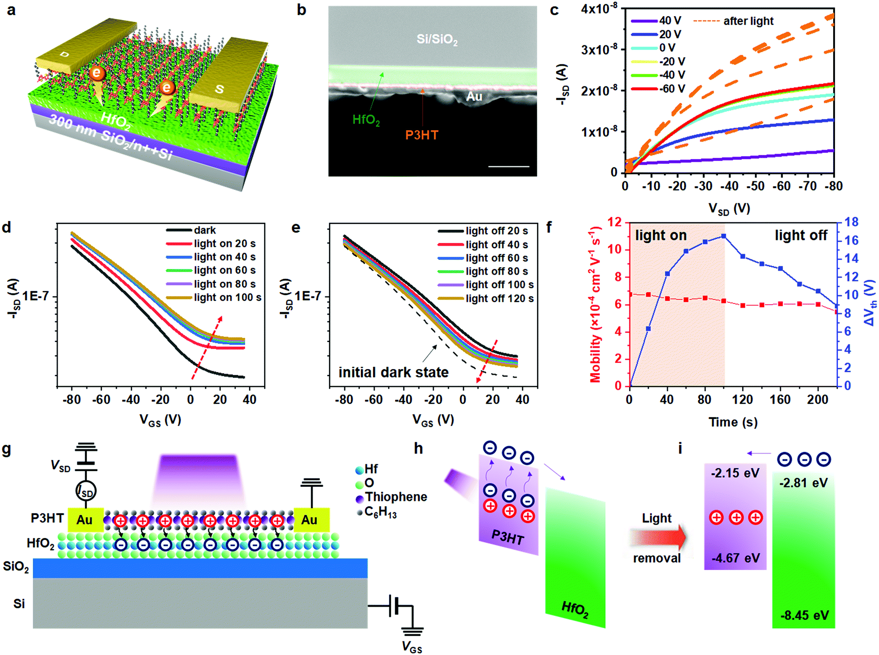 | ||
| Fig. 4 . Optoelectrical properties of P3HT crystals. (a) Schematic diagram of the phototransistor, where electrons are trapped at the interface between the P3HT crystal and HfO2 dielectric layer. (b) Cross-sectional SEM image of the device. (c) Representative output curves before (rainbow colours) and after (orange) light illumination. Wavelength = 405 nm. Intensity = 0.90 mW cm−2. (d) Light-dependent transfer curves of the device after the light was turned on. (e) Light-dependent transfer curves of the device after the light was turned off. (f) Change in the mobilities and the threshold voltages under or without light illumination, where the red line corresponds to the mobility trend, while the blue line represents the trend of threshold voltages change. (g) Schematic diagram of the transistor structure based on P3HT/HfO2 under 405 nm light illumination. P3HT is the transport channel. HfO2 and SiO2 are the dielectric gates. (h) According to the bandgap alignment, electrons were introduced into the LUMO of P3HT, and subsequently were trapped in the conduction band of HfO2, with the residual holes transported in the channel. (i) When the light illumination was turned off, the trapped electrons were gradually detrapped and recombined with the holes in the channel. | ||
Fig. 4d shows the light-dependent transfer curves of the device upon short term light illumination (405 nm, 0.90 mW cm−2) and the transfer curves with the light off are shown in Fig. 4e. In addition, the leakage current curves in both device configurations of Au/P3HT crystal/OTS-SiO2/Si and Au/P3HT crystal/HfO2/SiO2/Si are shown in Fig. S6d and e (ESI†), respectively. All the source-drain currents show significantly higher values than the leakage currents, indicating the normal operation of the device. Further, it can clearly be seen that the current in the device containing the OTS modifier was much higher compared with its leakage current, which can be attributed to the OTS-induced hydrophobicity. In addition, the suitable side chain length of OTS would sufficiently block the charge trapping at the interface. On the contrary, due to the charge transfer from the P3HT crystal to HfO2 at the interface, the drain current in the P3HT/HfO2-based device was much lower. Upon light illumination, the current of the device rapidly increased due to the generation of photo-excited carriers. The positive shift tended to be saturated after 100 s because the photo-generated excitons in the P3HT layer were saturated. After the light was turned off, the drain current slowly decreased and it was difficult for it to recover to the initial state, which is because the trapped electrons were slowly detrapped and recombined with holes. The change in the threshold voltage (ΔVth) and the mobility before and after illumination are summarized in Fig. 4f. The red line represents the fluctuation in mobility and the blue line represents the difference in value, which was calculated using the following equation.
| ΔVth = Vth,t − Vth,0 |
To vividly demonstrate the trapping/detrapping process before and after light illumination, the device structure and corresponding electron transfer in the transistor is plotted in Fig. 4g. The interface of P3HT and HfO2 can serve as a low-defect interface because atomic layer deposition is atomically precise vacuum deposition technology and the 2DCCPs transferred from the surface of the water also have molecularly flat undersurfaces.29 The LUMO and highest occupied molecular orbitals (HOMO) of P3HT are located at −2.15 eV and −4.67 eV, respectively. Meanwhile, the energy of the CB and valence band (VB) of HfO2 are −2.81 eV and −8.45 eV, respectively.30–32 As shown in Fig. 4h, excitons were introduced into the channel after light illumination, and subsequently separated into holes and electrons. Electrons in the LUMO of P3HT were trapped in the CB of HfO2 given that the LUMO of P3HT is slightly higher than the CB of HfO2. The positive shift in Vth and the clockwise hysteresis curve in Fig. S7a (ESI†) also prove the transfer of electrons.33 The inset figure is the microscopic image of the device array, and the channel length was calculated to be 36.4 μm. In addition, the I–V output curve of the device shown in Fig. S7b (ESI†) demonstrates a normal operation in a low voltage range. After the light was turned off, trapped electrons were gradually detrapped in the LUMO of P3HT and recombined with holes (Fig. 4i), leading to a slow drain current decay.
2.4. Photonic synaptic properties
The above-mentioned experiments demonstrated that our phototransistor can act as a PST, and thus the synaptic performances of this device were further characterized. Corresponding to the biological synapse shown in Fig. 5a, light spikes were regarded as the presynaptic inputs, while the drain currents were treated as postsynaptic signals, which are also regarded as the synaptic weight. All the experiments proceeded under high vacuum conditions (<10−6 mbar). The synaptic weight of the PST could be easily modulated through photo-generated exciton and HfO2-assisted electron transfer. Fig. 5b shows the short-term plasticity (STP) of the device, and the wavelength of the light source used in this experiment was 405 nm. One of the reasons for choosing the light source of 405 nm is that it is very close to the maximum absorption peak of the as-produced P3HT crystal (UV-vis spectrum of P3HT crystal is shown in Fig. S8a, ESI†) and that previously reported for P3HT in most solvents.34 Another reason is that the excitatory current of the device to 405 nm is of the highest, as shown in Fig. S8b (ESI†). The intensity of the light source was 0.90 mW cm−2. Under a constant drain voltage (VSD) of −80 V and gate voltage (VGS) of −80 V, when a light spike was applied, an enhanced postsynaptic current of 0.8 nA was attained at the end of the spike, which gradually descended towards the original state. Electrons were stimulated to the LUMO of P3HT under 405 nm light illumination and deeply trapped in the CB of HfO2. When the illumination was turned off, the trapped electrons were detrapped gradually and recombined with the holes in the P3HT channel, which resulted in typical postsynaptic current decay behaviour.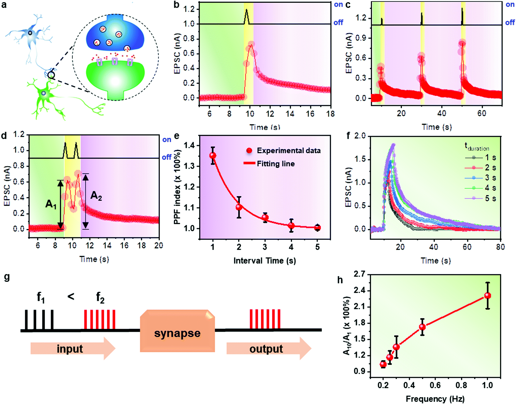 | ||
| Fig. 5 Photonic synaptic properties of the PST. (a) Schematic diagram of a biological neural system, where the synapse transmits presynaptic signals into postsynaptic signals through neurotransmitters. (b) STP trigged by a violet light spike (405 nm, 0.90 mW cm−2, 1 s) with a constant VSD of −80 V and VGS of −80 V. Left EPSC means excitatory postsynaptic current. (c) SIDP triggered by three different-intensity violet light spikes (0.45 mW cm−2, 0.90 mW cm−2, and 1.80 mW cm−2) with a constant VSD of −80 V and VGS of −80 V. The wavelength of the spike is 405 nm and its duration is 1 s. (d) PPF trigged by a pair of light spikes (0.90 mW cm−2, 1 s) with a constant VSD of −80 V and VGS of −80 V. (e) PPF indexes as a function of light spike intervals (ΔT). The light spike intensity was fixed at 0.90 mW cm−2 and the light spike width was 1 s. Error bars represent the standard error from three independent measurements of the PST. (f) EPSCs stimulated by 405 nm light spike with different illumination duration times. (g) Schematic illustration of the working mechanism of the high-pass filter. (h) Values of A10/A1 plotted as a function of the input frequencies. Error bars represent standard errors from three independent tests of the PST. | ||
Different-intensity light spikes were applied in one process, and then spike-intensity-dependent plasticity (SIDP) was performed, as shown in Fig. 5c, in which the applied light intensities were 0.45 mW cm−2, 0.90 mW cm−2 and 1.80 mW cm−2, respectively. Furthermore, the learning process of human brain could also be realized in our PST. The change in synaptic weight caused by a single light spike only lasted for a short duration, which can be compared to the short-term memory (STM) in the human brain. The STM could transform into long-term memory (LTM) after an intense and dense incoming stimulus was imposed (Fig. S9a, ESI†). Correspondingly, the STP could transform into long-term plasticity (LTP) in synaptic transistors.35 Our device performed preliminary LTP after a succession of illuminations, as shown in Fig. S9b (ESI†). The postsynaptic currents after the first and tenth illuminations were defined as A1 and as A10, respectively. When two adjacent light illuminations with an interval of 1 s were applied, the device exhibited an obvious paired-pulse facilitation (PPF) characteristic, as shown in Fig. 5d. This is because the light-introduced holes were not yet completely recombined after the first illumination was turned off, and another applied light illumination introduced more mobile holes in the channel. The postsynaptic current after the second illumination was defined as A2.35 When the light intervals were adjusted, the enhanced output signals were also tuned. The PPF indexes, which were calculated using the following equation, are summarized in Fig. 5e.
| PPF index = 100% × (A2/A1) |
PPF = 1 + C1![[thin space (1/6-em)]](https://www.rsc.org/images/entities/char_2009.gif) exp (−ΔT/τ1) + C2exp (−ΔT/τ2) exp (−ΔT/τ1) + C2exp (−ΔT/τ2) |
In the biological neuromorphic system, a special type of synapses can serve as a high-pass filter due to their low probability of initial neurotransmitter release. Only high-frequency (higher than a set cutoff value) signals could pass a high-pass filter, while lower-frequency signals were significantly hindered. The working mechanism of the filter is shown in Fig. 5g. Our PST presents application potential as a high-pass filter because after ten persistent spikes with a frequency of 1 Hz, a nearly 2.5-times enhanced output signal (A10/A1) could be achieved. Meanwhile, the lower-frequency persistent spikes induced an output signal that was enhanced by less than two. The values of A10/A1 were plotted as a function of input frequencies, as shown in Fig. 5h. It can clearly be seen that the value of A10/A1 is enhanced substantially with an increase in input frequency. Thus, another application dimension of a high-pass filter can be provided by our devices.
3. Conclusion
In summary, the space-confined drop-casting method was proven to be a general method for the efficient preparation of several different types of 2DCCPs on the surface of water. The self-shearing force generated by the evaporation of chloroform was proven to drive the ordered alignment of the polymer chains. The as-produced crystals were high quality with a thickness down to two molecular layers, while the lateral size of the crystal could reach the centimeter scale. Among the different 2DCCPs, the molecule chains of P3HT crystal were demonstrated to lay on the substrate in an edge-on configuration, as revealed by XRD, HR-TEM and SAED characterization. The transistor based on P3HT crystal/HfO2 possessed a light-dependent transfer characteristic and successfully realized the typical photonic synaptic properties, including STP, LTP, PPF and SIDP. Our work lays a solid foundation to prepare large-area integrated wireless communication systems and artificial visual systems based on centimeter-scale crystalline conjugated polymers.4. Experimental
4.1. 2DCCPs growth
Poly(3-hexylthiophene) (P3HT), poly(2,5-bis(3-hexadecylthiophen-2-yl)thieno[3,2-b]thiophene) (PBTTT-C16), poly[2,5-bis(3-tetradecylthiophen-2-yl)thieno[3,2-b]thiophene] (PBTTT-C14) and tetrabutylammonium bromide (TBAB) were purchased from Aladdin and used as received without further purification. P3HT, PBTTT-C16 and PBTTT-C14 were dissolved in chloroform with a concentration of 1 mg mL−1. Then, 50 mL DI water was added to the weighing bottles (70 mm × 40 mm) as a substrate. To ensure that there was a space-confined effect on the surface of DI water, TBAB was mixed in the DI water with a concentration of 12 mg mL−1. A droplet of solution containing the conjugated polymers was dropped onto the water surface for one minute. The emergence of thin films could be observed and the droplet gradually disappeared. After the solvent completely evaporated, free-standing 2DCCPs were floating on the water surface.4.2. Fabrication of FETs
Si/SiO2 wafers containing a 300 nm-thick SiO2 layer were treated by ultrasonication in DI water, and subsequently cleaned with piranha solution (7/3 vol/vol sulphuric acid/hydrogen peroxide) for ten minutes at 373 K. After natural cooling, the cleaned wafers were treated with oxygen plasma for about 10 min, and then immediately modified with octadecyltrichlorosilane (OTS) via a vapor phase method. The post-processing after modification included successive cleaning with hexane, chloroform and isopropanol. Free-standing P3HT crystals were transferred onto the surface of the OTS-modified Si/SiO2 wafers and the gold electrodes were thermally evaporated with the assistance of a mask.4.3. Fabrication of photonic synaptic transistors
Cleaned Si/SiO2 wafers without any modification were deposited with HfO2via the ALD method. The deposition rate was 1 Å s−1 and the final thickness of HfO2 was 20 nm. The transfer of P3HT films and the evaporation of gold electrodes were the same as that for the fabrication of the FETs.4.4. Characterization of materials and device properties
A Nikon ECLIPSE Ci-POL polarized optical microscope was utilized to take optical microscopic photos. TEM and HR-TEM measurements were conducted on a JEM-2800. The floating P3HT crystals were transferred onto carbon-supported Cu grids for TEM measurement. Powder XRD measurements were conducted on a Rigaku Smartlab diffractometer. Intelligent-mode AFM was performed using a Bruker Dimension Icon. Raman spectra and corresponding mappings were recorded using a confocal Raman spectrometer. SEM images were taken using a FESEM VERIOS 460. The FET characteristics were measured using a Keithley 4200-SCS. Synaptic transistors were wire-bonded onto chip carriers and loaded in a custom-designed high-vacuum system for the measurement of synaptic properties.Conflicts of interest
There are no conflicts to declare.Acknowledgements
Authors acknowledge the financial support from the Natural Science Foundation of China (Grants 52002267, U2032147, 21872100) and Singapore MOE Grant MOE-2019-T2-1-002.Notes and references
- J. V. Neumann, IEEE Ann. Hist. Comput., 1993, 15, 27 Search PubMed.
- E. Pereda, Nat. Rev. Neurosci., 2014, 15, 250 CrossRef PubMed.
- L. Abbott and W. G. Regehr, Nature, 2004, 431, 796 CrossRef PubMed.
- J. Gao, Y. Zheng, W. Yu, Y. Wang, T. Jin, X. Pan, K. P. Loh and W. Chen, Smart Mater., 2021, 2, 88 Search PubMed.
- F. Yang, L. Sun, Q. Duan, H. Dong, Z. Jing, Y. Yang, R. Li, X. Zhang, W. Hu and L. Chua, Smart Mater., 2021, 2, 99 Search PubMed.
- J. Heeger, Chem. Soc. Rev., 2010, 39, 2354 RSC.
- X. Pan, Y. Zheng, Y. Shi and W. Chen, ACS Mater. Lett., 2021, 3, 235 CrossRef CAS.
- D. H. Kim, J. T. Han, Y. D. Park, Y. Jang, J. H. Cho, M. Hwang and K. Cho, Adv. Mater., 2006, 18, 719 CrossRef CAS.
- V. Chaudhary, R. K. Pandey, R. Prakash, N. Kumar and A. K. Singh, Synth. Met., 2019, 258, 116221 CrossRef CAS.
- C. Xu, P. He, J. Liu, A. Cui, H. Dong, Y. Zhen, W. Chen and W. Hu, Angew. Chem., Int. Ed., 2016, 55, 9519 CrossRef CAS.
- Q. Wang, F. Yang, Y. Zhang, M. Chen, X. Zhang, S. Lei, R. Li and W. Hu, J. Am. Chem. Soc., 2018, 140, 5339 CrossRef CAS.
- H. Dong and W. Hu, Acc. Chem. Res., 2016, 49, 2435 CrossRef CAS.
- H. Dong and W. Hu, Acta Polym. Sin., 2017, 8, 1246 Search PubMed.
- H. Dong, S. Jiang, L. Jiang, Y. Liu, H. Li, W. Hu, E. Wang, S. Yan, Z. Wei, W. Xu and X. Gong, J. Am. Chem. Soc., 2009, 131, 17315 CrossRef CAS.
- Z. Shu, Q. Zhang, P. Zhang, Z. Qin, D. Liu, X. Gao, B. Guan, H. Qi, M. Xiao, Z. Wei, H. Dong and W. Hu, Polym. Chem., 2020, 11, 1572 RSC.
- C. Li, Y. Wang, Y. Zou, X. Zhang, H. Dong and W. Hu, Angew. Chem., Int. Ed., 2020, 59, 9403 CrossRef CAS PubMed.
- Y.-S. Guan, A. Thukral, S. Zhang, K. Sim, X. Wang, Y. Zhang, F. Ershad, Z. Rao, F. Pan, P. Wang, J. Xiao and C. Yu, Sci. Adv., 2020, 6, eabb3656 CrossRef CAS.
- H. Sirringhaus, P. Brown, R. Friend, M. M. Nielsen, K. Bechgaard, B. Langeveld-Voss, A. Spiering, R. A. Janssen, E. Meijer and P. Herwig, Nature, 1999, 401, 685 CrossRef CAS.
- M. Bag, T. S. Gehan, D. D. Algaier, F. Liu, G. Nagarjuna, P. M. Lahti, T. P. Russell and D. Venkataraman, Adv. Mater., 2013, 25, 6411 CrossRef CAS PubMed.
- J. Wang, J. Niu., B. Shao, G. Yang, C. Lu, M. Li, Z. Zhou, X. Chuai, J. Chen, N. Lu, B. Huang, Y. Wang, L. Li and M. Liu, Nat. Commun., 2021, 12, 58 CrossRef CAS PubMed.
- M. K. Singh, A. Kumar and R. Prakash, Org. Electron., 2017, 50, 138 CrossRef CAS.
- J. Xu, H.-C. Wu, C. Zhu, A. Ehrlich, L. Shaw, M. Nikolka, S. Wang, F. Molina-Lopez, X. Gu, S. Luo, D. Zhou, Y.-H. Kim, G.-J. N. Wang, K. Gu, V. R. Feig, S. Chen, Y. Kim, T. Katsumata, Y.-Q. Zheng, H. Yan, J. W. Chung, J. Lopez, B. Murmann and Z. Bao, Nat. Mater., 2019, 18, 594 CrossRef PubMed.
- M. Rahmani, L. Jerbi and A. Meftah, J. Lumin., 2020, 217, 116805 CrossRef.
- D. Xiang, C. Han, J. Wu, S. Zhong, Y. Liu, J. Lin, X. Zhang, W. Hu, B. Özyilmaz, A. H. C. Neto, A. T. S. Wee and W. Chen, Nat. Commun., 2015, 6, 6485 CrossRef PubMed.
- Y. Zheng, Z. Hu, C. Han, R. Guo, D. Xiang, B. Lei, Y. Wang, J. He, M. Lai and W. Chen, Nano Res., 2019, 12, 531 CrossRef.
- J. Gao, H. Yang, H. Mao, T. Liu, Y. Zheng, Y. Wang, D. Xiang, C. Han and W. Chen, Adv. Opt. Mater., 2020, 8, 1901971 CrossRef.
- D. Kim, J. Han, Y. D. Park, Y. Jang, J. H. Cho, M. Hwang and K. Cho, Adv. Mater., 2006, 18, 719 CrossRef.
- A. Abutaha, P. Kumar, E. Yildirim, W. Shi, S.-W. Yang, G. Wu and K. Hippalgaonkar, Nat. Commun., 2020, 11, 1737 CrossRef PubMed.
- B. S. Lim, A. Rahtu and R. G. Gordon, Nat. Mater., 2003, 2, 749 CrossRef PubMed.
- J.-H. Kim, J.-A. Hong, D.-G. Kwon, J. Seo and Y. Park, Appl. Phys. Lett., 2014, 104, 163303 CrossRef.
- J. H. Choi, Y. Mao and T. P. Chang, Mater. Sci. Eng., R, 2011, 72, 97 CrossRef.
- J. Robertson and R. M. Wallace, Mater. Sci. Eng., R, 2015, 88, 1 CrossRef.
- N. Kaushik, D. M. A. Mackenzie, K. Thakar, N. Goyal, B. Mukherjee, P. Boggild, D. H. Petersen and S. Lodha, npj 2D Mater. Appl., 2017, 1, 34 CrossRef.
- Y. Na and F. S. Kim, J. Nanosci. Nanotechnol., 2020, 20, 491 CrossRef.
- X. Pan, T. Jin, J. Gao, C. Han and W. Chen, Small, 2020, 16, 2001504 CrossRef.
- R. A. John, N. Yantara, Y. F. Ng, G. Narasimman, E. Mosconi, D. Meggiolaro, M. R. Kulkarni, P. K. Gppalakrishnan, C. A. Nguyen, F. D. Angelis, S. G. Mhaisalkar, A. Basu and N. Mathews, Adv. Mater., 2018, 30, 1805454 CrossRef.
- R. S. Zucker and W. G. Regehr, Annu. Rev. Physiol., 2002, 64, 355 CrossRef PubMed.
Footnote |
| † Electronic supplementary information (ESI) available. See DOI: 10.1039/d1tc02284a |
| This journal is © The Royal Society of Chemistry 2022 |