
 Open Access Article
 This Open Access Article is licensed under a
 Creative Commons Attribution 3.0 Unported Licence
ZnO–PTFE-based antimicrobial, anti-reflective display coatings and high-sensitivity touch sensors†
Swathi
Ippili
*,
Venkatraju
Jella
*,
Jeong Min
Lee
,
Jang-Su
Jung
,
Dong-Hyun
Lee
,
Tae-Youl
Yang
and
Soon-Gil
Yoon
 *
*
Department of Materials Science and Engineering, Chungnam National University, Daeduk Science Town, 34134, Daejeon, Republic of Korea. E-mail: sgyoon@cnu.ac.kr; venkatrajujella@gmail.com; iswathirs@gmail.com
First published on 23rd September 2022
Abstract
Due to the rapid transmission of bacterial infections via microbial-contaminated interactive touch devices, functional coatings that can eradicate microbial contamination are in high demand. Furthermore, flexible and transparent antimicrobial touch/tactile sensors have received considerable attention on account of their wider applicability in personal electronic devices. Herein, anti-reflective, hydrophobic, antimicrobial zinc oxide-polytetrafluoroethylene (ZnO–PTFE) composite thin films with sensorial capabilities are developed via a sputtering technique. The ZnO–PTFE exhibits a significantly low refractive-index, high transmittance, and excellent hydrophobic properties, along with outstanding antibacterial activities of ∼6.2 and ∼4.7 for E. coli and S. aureus, respectively. Importantly, the major issue of zinc dissolution in water from the ZnO material is controlled in this study by compositing with PTFE to realize long-term water-stability and mechanical durability of ZnO films. Further, a triboelectric nanogenerator (TENG) based antimicrobial self-powered touch sensor that delivered recordable pressure/touch sensitivity is developed based on ZnO–PTFE composite films. In which, the ZnO–PTFE composite-based TENG is shown to provide a high triboelectric output voltage of ∼224 V, a current density of ∼21.4 μA cm−2, and a power density of 1.65 mW cm−2. Furthermore, the linear response of the TENG to driven pressure indicates its excellent pressure-sensing ability, with an unprecedented sensitivity of 75.31 V kPa−1 and a touch sensitivity of 31.36 V kPa−1. Further, the real-time application of ZnO–PTFE as a display coating and self-powered touch sensor is demonstrated. This work demonstrates a simple route towards the design of smart antimicrobial coatings with multifunctional capabilities for a wide range of applications in interactive devices for a safer experience.
1. Introduction
Infectious diseases caused by harmful pathogens present a rapidly increasing threat to human beings and the global economy.1 Rapid transmission of infectious diseases from person to person mainly arises from microbial contamination of the surrounding environment.2 Nowadays, touch-enabled displays are widely and commonly used around the world in personal devices, smart appliances, and public access machines. These touch-enabled displays are said to be a source of pathogens such as bacteria, viruses, fungi, and parasites, thereby causing significant spread of infectious diseases to human beings.3–5 In addition, the outbreak of Covid-19 has raised public awareness of the disinfection pathways of such highly infectious microbes and the need for hygiene in order to combat the extensive contamination of public touchscreens.6 Cleaning and disinfection are effective measures for preventing the spread of pathogens from contaminated surfaces.7 However, because there is a high possibility of recontamination within a short time, frequent cleaning is required.8 Moreover, some manufacturers advise against the use of chemical disinfectants such as ethanol and isopropanol for cleaning touchscreens due to the sensitivity of touchscreens.9 In this respect, antimicrobial coatings are a potential solution for preventing the bacterial contamination of touchscreens. In particular, metal and metal oxide-based nanomaterials have been widely used as antimicrobial coatings because their small size and high specific surface area make them highly toxic to pathogens.10,11 Specifically, the broad-spectrum antimicrobial activity of ZnO has been extensively investigated because of its biosafety, biocompatibility, and low cost due to its abundance in nature.12–17 Recent studies have also shown that ZnO coatings effectively reduce the infectivity of severe acute respiratory syndrome coronavirus-2 (SARS-CoV-2) within 1 h of contact with the virus.18 Due to their agglomeration and weak adhesion to the substrate, solution-processed ZnO NP-based films may not provide high transmittance and good mechanical durability required of touchscreens.19 However, these requisite properties, along with excellent antimicrobial activity, have been exhibited by sputtered ZnO thin films.20Another important strategy is the development of hydrophobic antibacterial coatings that reduce the adhesion force between microorganisms and the surface, thus leading to the removal of bacteria from the surface even before a biofilm can form.21 In addition, when applied to touchscreens, hydrophobic antibacterial coatings can provide anti-fingerprinting properties. Although the above-mentioned metal oxide thin films are hydrophilic in nature,20,22 the commonly used water repellant polymer, polytetrafluoroethylene (PTFE), has been used to provide antibacterial coatings with the desired hydrophobic properties and excellent mechanical properties without degrading the antibacterial activity.23,24 For example, S. Y. Heo et al. reported that the coating of sputtered silver with a 15 nm thick PTFE protective film significantly improved the anti-fingerprint nature and mechanical durability of the antibacterial film.25 Moreover, a previous study by the present authors showed that an ultrathin PTFE coating on zinc-doped silicon oxide (SZO) noticeably increased the hydrophobicity and antireflective ability of antibacterial SZO/PTFE thin films.26
Touch sensors have received widespread attention in current research for applications including e-skins, artificial prosthetics, robotics, and healthcare monitors.27 In particular, the development of flexible self-powered touch sensors is highly essential for flexible and wearable electronic applications. Triboelectric nanogenerators (TENGs) and piezoelectric nanogenerators (PENGs) directly convert mechanical stimuli into electrical signals,28–31 and have been extensively used for energy-harvesting and self-powered sensor applications.32,33 In this respect, triboelectric pressure sensors have the capability of converting weak mechanical stimuli into higher potentials than can the piezoelectric pressure sensor.32,34 However, because they are operated with frequent contact, touch sensors are excellent media for the growth of microorganisms, thereby increasing the threat to human health. Hence, a few recent studies have reported the use of antibacterial triboelectric TENGs for energy-harvesting and sensor applications.35 For instance, Ma et al. demonstrated a self-powered antibacterial tactile sensor based on the triboelectric and piezoelectric coupling effects of PTFE/silver nanowires (Ag NWs) and polyvinylidene fluoride (PVDF) films.36 Similarly, PLGA/Ag NWs/PVA nanofiber film-based TENGs have been reported for antimicrobial self-powered e-skin application.37 However, most of these studies used TENGs based on thick and opaque films for antibacterial pressure sensor applications.
In the present study, flexible, eco-friendly ZnO–PTFE composite films are demonstrated as anti-reflective, hydrophobic, antibacterial surface coatings and self-powered antibacterial touch sensors. Transparent ZnO–PTFE thin films with various amounts of PTFE are fabricated by co-sputtering at a fixed power of 60 W for ZnO and various powers for PTFE, and their transmittance, anti-reflectance, hydrophobic, and antibacterial properties are investigated. Further, the ZnO–PTFE thin films are applied as active materials in TENG devices, and their triboelectric outputs are shown to increase with increasing PTFE content. In particular, the TENG based on the co-sputtered film with the highest amount of PTFE exhibits a high-power density of 1.65 mW cm−2, an excellent pressure sensitivity of 75. 2 V kPa−1, and a touch sensitivity of 31.36 V kPa−1, thereby demonstrating the potential application of the device as an antibacterial touch sensor.
2. Experimental
2.1. Deposition of the ZnO–PTFE composite thin films
The flexible ZnO–PTFE composite thin films were deposited onto commercially available indium tin oxide-coated polyethylene terephthalate (ITO/PET) substrates at room temperature via an on-axis gun radio frequency (RF) co-sputtering method, as schematically shown in Fig. S1 of the ESI.† Prior to sputtering, the surfaces of the two-inch diameter ZnO and PTFE targets were cleaned by abrasion with sand paper, and the substrates were cleaned by ultrasonication in ethanol and deionized (DI) water for 10 min each, followed by drying under nitrogen gas. A fixed RF power of 60 W was used for the ZnO target, and various RF powers of 10, 25, 40, and 60 W were used for the PTFE target in order to regulate the polymer content of the ZnO–PTFE composite thin films. The as-obtained samples are hereafter referred to as ZP-10, ZP-25, ZP-40, and ZP-60, respectively. The sputtering process was performed at a fixed working pressure of 20 mtorr under an argon (10 sccm) atmosphere. For comparison, neat ZnO and neat PTFE thin films were separately deposited at a fixed RF power of 60 W. The complete sputtering conditions are listed in Table S1.† Prior to the deposition of all thin films, a pre-sputtering process was performed for around 30 min in order to remove any contamination from the surfaces of the targets.2.2. Construction of the ZnO–PTFE thin film-based TENGs
To fabricate the flexible and eco-friendly ZnO–PTFE thin film-based TENGs with the structure of PET/ITO/ZnO–PTFE//PET, the as-sputtered ZnO–PTFE film on the ITO/PET substrate (PET/ITO/ZnO–PTFE) was sandwiched with a bare PET substrate using a 5 mm thick polyurethane sponge, such that the PET surface faced the ZnO–PTFE film. The TENG with a size of 3 × 3 cm2 and an active area of 1 × 1 cm2 was then completed by using silver paste and carbon tape to attach the copper wires for electrical connection. However, for characterizing the ZnO–PTFE TENG as a touch/tactile sensor, the TENG is tapped with a bare finger instead of a bare PET film.2.3. Characterization of the ZnO–PTFE composite thin films and the TENGs
The phases, chemical states, and crystallinities of the as-sputtered ZnO–PTFE films were characterized by grazing incidence X-ray diffraction (GIXRD, Rigaku D/MAX-RC) using Cu Kα radiation, and by X-ray photoelectron spectroscopy (XPS, MULTILAB 2000, Thermo Fisher Scientific). The variations in surface morphology, surface roughness, and thickness of the films were characterized via atomic force microscopy (AFM, Asylum Research, Oxford instruments). In addition, the morphology was investigated via field emission scanning electron microscopy (FE-SEM, TOPCON DS-130C), and the elemental distributions within the composite films were examined via scanning electron microscopy combined with energy dispersive X-ray spectroscopy (SEM-EDS). The transmittance of each film was studied using an ultraviolet-visible (UV-vis) spectrophotometer (S-3100, SCINCO CO., LTD.), and the refractive index was measured at a wavelength of ∼630 nm via ellipsometry (M-2000 Ellipsometer, J.A. Woollam). The hydrophobic nature of each film was determined via drop shape analysis (DSA 100, Kruss Co.) under ambient conditions. For this procedure, a drop of deionized (DI) water with a constant volume of ∼20 μL was decanted onto the film surface, and the water contact angle (WCA) was evaluated by examining a photograph. The dielectric properties (capacitance and dissipation factor) of the as-fabricated films were examined using an impedance/gain-phase analyzer (Hewlett Packard 4194A) and a metal-insulator-metal (MIM) device structure with a 150 μm diameter DC-sputtered Ti/Au (10 nm/80 nm) top electrode and an ITO glass bottom electrode similar to earlier reports.38–41 The nanoindentation measurements were performed to estimate the elastic modulus and hardness of the thin film using an i-Micro indenter (KLA Instruments, USA) equipped with a Berkovich indenter. The indentation tests were carried at a constant indentation strain rate of 0.2 s−1 for 150 nm-thick films and the maximum depth was set as ∼20 nm (i.e. 10% relative indention depth of the film) in order to avoid the substrate effect.The antibacterial activities of 30 nm thick ZnO–PTFE composite films (specifically, ZP-10 and ZP-60) fabricated on glass substrates (5 × 5 cm2, Corning EAGLE XG Glass) were tested at the FITI Testing and Research Institute (Korea) using the Japanese industrial standard film attachment method (JIS Z 2801).42 For these tests, Staphylococcus aureus (S. aureus, American Type Culture Collection no. 6538P) was used as the Gram-positive bacteria, and Escherichia coli (E. coli, American Type Culture Collection no. 8739) was used as the Gram-negative bacteria. For comparison, the same tests were performed on neat eagle glass substrates without any active ZnO–PTFE composite films. A set of five samples were used for each test, and the data were averaged. The details of the antibacterial activity tests are provided in an earlier study.20
The triboelectric output performances of the as-constructed ZnO–PTFE TENGs were characterized under continuous contact-separation mode with an applied pressure using a customized mechanical pushing tester consisting of a 1 × 1 cm2 pushing stack. The mechanical force was applied normal to the device, and was instantaneously monitored using a load cell (Dacell UU-K20). The obtained open-circuit voltage and short-circuit current signals were respectively recorded using a digital phosphor oscilloscope (DPO 5204B, Tektronix) with a 10 MΩ impendence probe and a low-noise current amplifier (SR570, Stanford Research Systems).
3. Results and discussion
3.1. Compositional analysis and characterization of the ZnO–PTFE composite films
The PTFE polymer is selected for fabricating flexible ZnO–PTFE composite films via a radio-frequency co-sputtering method (Fig. S1†) because of its beneficial features, including corrosion resistance, self-cleaning, mechanical durability, water-repellency, non-toxicity, high-transparency, and low refractive index, making it highly desirable for application as a surface coating material for various displays, medical devices, and fabrics.26,43,44 The phases and crystallinities of the ZnO–PTFE composite films with 150 nm thickness are revealed by the XRD results in Fig. 1a. Here, the XRD pattern of the neat PTFE film exhibits a broad peak at a 2θ value of around 22°, which is related to the glass substrate and indicates the presence of the amorphous polymer phase. Meanwhile, the neat ZnO films exhibit diffraction peaks at 2θ values of 34.59°, 36.38°, and 47.71° corresponding to the (002), (101), and (102) planes, respectively, of the typical hexagonal wurtzite structure of ZnO (JCPDS, File no. 036-1451).45 Similar peaks are observed in the ZnO–PTFE composite films, but with increasing intensity as the sputtering power of the PTFE target is increased up to 40 W. With further increase in the PTFE power to 60 W, however, the ZP-60 film exhibits a new diffraction peak at 2θ = 31.9°, corresponding to the (100) plane of ZnO. In addition to the ZnO phase, the enlarged XRD pattern in Fig. S2† reveals the presence of a secondary ZnF2 phase, as indicated by the diffraction peaks at 2θ = 26.89° and 34.9°.46 | ||
| Fig. 1 Chemical characterization of the various ZnO–PTFE composite films: (a) the XRD patterns; (b–e) the XPS full scan (b) and core-level zinc (c), fluorine (d), and carbon (e) spectra; (f) the SEM-EDS elemental mapping images of the ZP-60 thin films deposited on glass substrates. | ||
The presence of the elements C and F in the PTFE films is revealed by the XPS C 1s and F 1s data in Fig. S3.† There, the core-level C 1s spectrum is fitted to multiple peaks with binding energies of around 291.7, 289.6, 287.6, and 285.3 eV corresponding to the –CF2, C–F, C–CF, and C–C bonds of PTFE, respectively,47 and the F 1s peak located at around 687 eV is characteristic of the fluorine atoms of the C–F bonds. The full scan XPS spectra of all the ZnO–PTFE films are compared in Fig. 1b, confirming the co-existence of Zn, O, F, and C elements. Moreover, the magnified Zn 2p spectrum in Fig. 1c exhibits peaks at around 1021.4 and 1044.5 eV corresponding to the Zn 2p3/2 and 2p1/2, respectively.48 However, these peaks are shifted towards higher binding energies for the ZP-60 films. Meanwhile, the core-level F 1s spectra of the ZP-10 and ZP-60 samples in Fig. 1d each exhibit a main peak at around 686.5 eV corresponding to the C–F bond of the PTFE polymer, along with low intensity peaks at around 684.7 eV and 687.2 eV, indicating the presence of the ZnF2 phase and CF3 of the PTFE polymer, respectively, which are absent from the neat ZnO film.49 In addition, the ZP-60 film exhibits a relatively higher ratio of fluorine to zinc (Table 1), which is attributed to the higher power applied to the PTFE target. Moreover, the core-level C 1s and O 1s spectra are also fitted into multiple peaks in Fig. 1e and S4,† respectively.49,50 Particularly, the fitted core-level C 1s spectrum of ZP-60 with binding energies of around 284.8, 290, and 293.8 eV correspond to the C–C, C–F, and CF3 of PTFE, respectively, which are absent from the neat ZnO and ZP-10 films,49 whereas the peaks around 286, and 287.7 eV correspond to the C–O/C–N, and C![[double bond, length as m-dash]](https://www.rsc.org/images/entities/char_e001.gif) O bonds, related to the weak bonds of carbon with oxygen/nitrogen on the surface.
O bonds, related to the weak bonds of carbon with oxygen/nitrogen on the surface.
| Sputtered films | C (at%) | Zn (at%) | O (at%) | F (at%) |
|---|---|---|---|---|
| Neat ZnO | 27.47 | 34.27 | 38.26 | — |
| ZP-10 | 27.89 | 32.39 | 37.87 | 1.86 |
| ZP-60 | 21.66 | 17.52 | 14.19 | 46.64 |
| Neat PTFE | 38.81 | — | — | 61.19 |
Samples of the various thin films with a consistent thickness of 30 nm were selected for SEM analysis. The selected film thickness is confirmed by the AFM height profiles in Fig. S5,† and the corresponding SEM images are presented in Fig. S6.† In the SEM images, the particle-like surface morphologies of the sputtered films are seen to vary according to the PTFE contents, such that the particle size is significantly decreased as the PTFE content is increased, thereby resulting in an increasingly dense surface. In addition, an amorphous polymer network is observed for both the ZP-60 and neat PTFE films, thereby indicating the uniform distribution of ZnO in the PTFE matrix. Further, the EDS mapping images of O and Zn given in Fig. 1f and S7† clearly demonstrate the uniform growth of ZnO in the as-synthesized ZP-60 and neat ZnO films, while the C and F mappings of the ZP-60 film in Fig. 1f clearly validate the uniform distribution of ZnO in the PTFE matrix to form a ZnO–PTFE composite film. In addition, it is reported that the dissolution of Zn ions from the ZnO films during water dipping causes the functional and morphological changes of ZnO films.22 Therefore, the water stability of the neat ZnO and ZP-60 films was analyzed from the SEM images after dipping the films into deionized (DI) water under ambient dark conditions. The SEM surface images of neat ZnO thin films reveal significant changes in the surface morphology after dipping in water (within 1 day of dipping) (Fig. S8†) as clearly seen holes/gaps throughout the surface due to the release of Zn ions from the ZnO. These gaps are further increased and cause delamination of the film from the substrate with increasing the dipping time to 10 days. On the other hand, no notable changes in the surface morphology were perceived in the ZP-60 films even after long time (for 10 days) dipping in water (Fig. 2a, b, and S9a), which could be due to passivation of the ZnO material by the PTEF polymer that significantly reduces the direct interaction of water with the ZnO material. In addition, the effects of water dipping tests on the transmittance of ZP-60 films were investigated. The ZP-60 films exhibited similar transmittance values compared to those of as-deposited ZP-60 films even after 10 days of water dipping (Fig. S9b†). From the results, it is concluded that the ZnO–PTFE composite films exhibit good water stability even after dipping into water for a long time. Meanwhile, the AFM images of the various ZnO–PTFE composite films in Fig. S10† reveal dense and smooth surfaces with relatively low root mean square (rms) roughnesses (≤1.3 nm). Further, the bar chart of AFM-RMS roughness against the PTFE content in Fig. 2c clearly demonstrates that the surface roughness significantly decreases with increasing PTFE sputtering power, such that the roughness of the ZP-60 film (0.43 nm) is closely comparable to that of the neat PTFE film (0.41 nm). In general, the samples having low surface roughness exhibit high transparency characteristics.26 Therefore, the low surface roughness values of ZnO–PTFE composite films could be beneficial for obtaining high transparency of the composite films.
 | ||
| Fig. 2 Surface morphology, transmittance, reflectance, hydrophobic, and antimicrobial characteristics of the various ZnO–PTFE composite films: SEM surface morphology of water dipped ZP-60 films: (a) as-deposited (before dipping), and (b) after 10 days dipping into DI water. (c) The AFM-RMS roughness; (d) the UV-Vis transmittance; (e) the refractive index; (f) the water contact angles; (g) load-displacement curves obtained by nanoindentation, and the corresponding (h) elastic modulus and (i) hardness. | ||
3.2. Anti-reflectance, hydrophobic, and mechanical properties of the ZnO–PTFE composite films
The UV-vis transmission spectra of the 30 nm thick ZnO–PTFE composite films are compared with those of the neat ZnO and neat PTFE films in Fig. 2d. Here, the neat ZnO film exhibits a transmittance of ∼83%, which is much lower than that of the neat PTFE film (∼91.6%). However, the transmittance characteristics of the ZnO–PTFE films are considerably improved with increasing PTFE amount, such that the ZP-60 film exhibits a comparatively high transmittance of ∼87.4%. The achieved high transmittance of ZP-60 films might be due to the decrease in the surface roughness that reduces the reflectance of light, resulting in significant improvement in the transmittance of the composite films. In addition, the ellipsometry results in Fig. 2e indicate that the anti-reflectance properties of the ZnO–PTFE films are progressively and significantly improved with the increase in the amount of PTFE. Thus, while the neat ZnO film displays a much higher refractive index (n = 1.72) than that of the neat PTFE thin film (n = 1.39),51,52 the ZP-60 film has a significantly decreased refractive index of only 1.54, which is similar to that of the glass substrate (i.e., 1.52).53 This might be attributed to the encapsulation of ZnO by the PTFE polymer. Moreover, the appearance of the ZnF2 phase in the ZP-60 films might provide lower n values because of its lower n value compared to the ZnO material.54 The hydrophobic properties of 30 nm thick neat ZnO and ZnO–PTFE composite films are demonstrated by the WCA measurements and corresponding digital images in Fig. S11.† Here, the neat ZnO film exhibits hydrophilic nature with a much lower WCA value (∼31°) than those of the PTFE-containing film, which might be attributed to the native oxygen vacancies in the film.26 However, the hydrophobicity of the ZP-60 (WCA of ∼91°) is significantly increased due to PTFE polymer passivation. Further, the hydrophobic properties of the 100 nm thick ZnO–PTFE composites are analyzed and the corresponding digital images are given in Fig. 2f. The hydrophobicity of ZP-10 is significantly increased relative to that of the neat ZnO, and the hydrophobicity continues to increase gradually with increasing PTFE content. Consequently, the ZP-60 film has a high WCA value of 105.2°, which is closely comparable to that of the neat PTFE film (i.e., 108.5°). These results unambiguously prove that PTFE can not only assist in increasing the hydrophobicity, but also improve the anti-reflectance properties of the oxide materials. Further, mechanical properties such as the elastic modulus and hardness were investigated for the composite films. Unlike bulk polymer composite films that utilize a universal testing machine to investigate the mechanical properties of polymers, the nanoindentation method was implemented in this study to investigate the mechanical properties of ZnO–PTFE sputtered thin films with a thickness of 150 nm.55,56 The reason for using high thickness films is to eliminate the substrate effect contribution for the mechanical properties of composite films. The typical load–displacement curves of ZnO–PTFE composite films along with neat ZnO and neat PTFE films shown in Fig. 2g reveal a perceptible dependence of indent formation on the content of PTFE in ZnO–PTFE composite films. In particular, the slope of the load–displacement curves continuously decreased with increasing the PTFE content in the composite films. The average elastic modulus (E) and hardness (H) were evaluated from the load–displacement curves obtained for 20 distinct indents for each sample (Fig. 2h and i). The elastic modulus and hardness of neat ZnO (96.12 ± 4.38 GPa and 8.57 ± 0.67 GPa) were much higher than those of the neat PTFE films (18.55 ± 1.05 GPa and 0.71 ± 0.04 GPa). However, both the elastic modulus and hardness of the composite films were continuously decreased with increasing the PTFE content. In particular, ZP-60 films unveiled a relatively low elastic modulus of 83.01 ± 5.08 GPa and hardness of 5.21 ± 0.66 GPa compared with other composite films and the neat ZnO film. In addition, to confirm the mechanical robustness of the composite films, the hand bending test (bending radius of around 5 mm) was performed for 30 nm thick neat ZnO and ZP-60 films sputtered on a flexible PET substrate. Several cracks were observed for neat ZnO films after 2000 bending cycles, as seen in SEM images (Fig. S12a†), while no noticeable changes in surface morphologies were observed for the ZP-60 films under harsh bending tests (Fig. S12b†). Further, the abrasive tape test using poly imide tape was also conducted to examine the adhesion properties of ZP-60 composite films. The optical microscopy images (in surface view) and corresponding UV-transmittance spectra portrayed in Fig. S13a, and b,† respectively, reveal no clear changes in both surface and transparency values even after performing tape tests for 500 times, indicating the excellent mechanical stability and adhesion properties of ZnO–PTFE composite thin films. These properties are indispensable requirements for the functional coating material.3.3. Antimicrobial properties of the ZnO–PTFE composite films
E. coli and S. aureus are the major pathogens that can cause a variety of serious community and nosocomial (hospital-acquired) infections. Moreover, recently observed antibiotic resistant nature of these bacteria to many antibiotics is a major concern in the global public health. Therefore, the antibacterial activity of ZnO–PFTE composite films was investigated against E. coli and S. aureus bacterial strains in the present study. The antimicrobial activities of 30 nm thick ZP-10 and ZP-60 composites against S. aureus and E. coli are compared with that of blank glass after an incubation period of 24 h in Fig. 3a and b, respectively, and the results are summarized in Fig. 3c. The photographs in Fig. 3a-1 and b-1 indicate that both S. aureus and E. coli remain alive on the bare glass substrate, thereby signifying no antimicrobial properties. However, significant reduction in S. aureus and E. coli bacteria is clearly observed on the various ZnO–PTFE composite films after incubation (Fig. 3a-2, a-3, b-2 and b-3). Notably, both the ZP-10 and ZP-60 samples with high and low zinc concentrations reveal similar antimicrobial properties. In detail, each film affords a percentage reduction of 99.9803% and 99.9999% against S. aureus and E. coli, respectively (Fig. 3c), thereby signifying no distinct change in the antimicrobial properties of the composite films with increasing amounts of PTFE polymer. Further, the efficiency of the antimicrobial thin films can be estimated by using the formula:| Antibacterial activity = log(bacteria population on blank after 24 h of incubation) − log(bacteria population on target sample after incubation) |
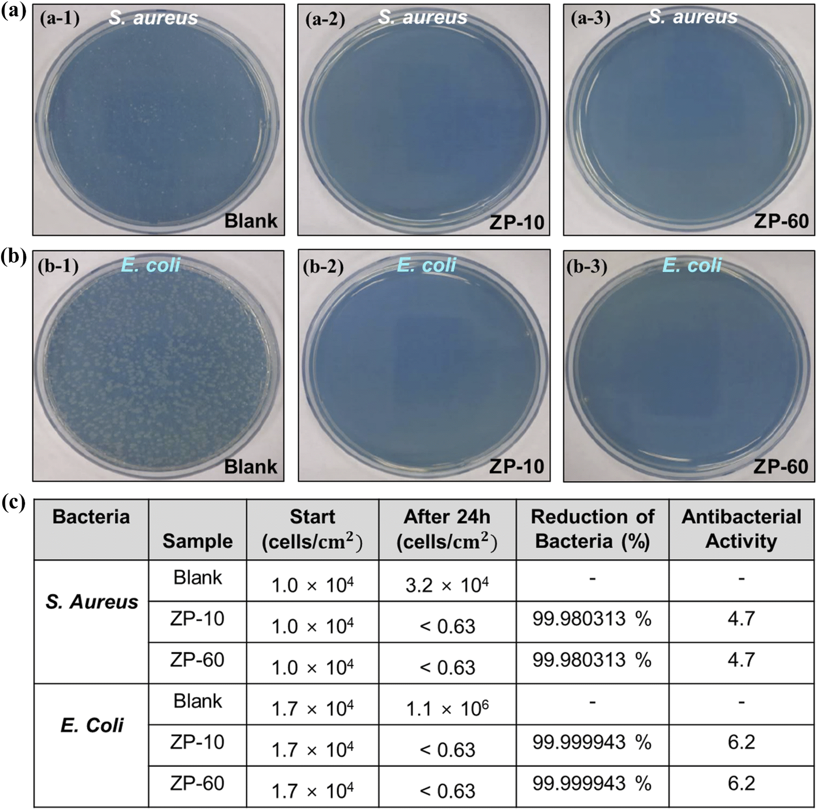 | ||
| Fig. 3 Antimicrobial characteristics of the various ZnO–PTFE composite thin films: (a and b) digital images of the antibacterial tests against S. aureus (a) and E. coli (b) after incubation for 24 h on bare glass (a-1 and b-1), the ZP-10 film (a-2 and b-2), and the ZP-60 film (a-3 and b-3). (c) The percentage reduction of S. aureus and E. coli by the ZP-10 and ZP-60 composite thin films. | ||
| Material | Method | Type | Reduction of bacteria/zone diameters (S. aureus and E. coli) | Antibacterial activity | Ref |
|---|---|---|---|---|---|
| ZnO | Solution | Bulk | 38.1% | — | 17 |
| 5% Ng/Cu-doped ZnO | Solution | Bulk | ∼38% | — | 16 |
| CNCFs + Ag NPs | Solution | Bulk | 16.3 mm and 14.4 mm | — | 58 |
| NCESP-Ag NPs | Solution | Bulk | 35 mm and 33 mm | — | 59 |
| SZO/PFTE | Sputtering | Thin film | 99.99991% and 99.998909% | 4.6 and 6.3 | 26 |
| ZnO | Sputtering | Thin film | 99.99668% and 99.99999% | 4.3 and 6.1 | 11 |
| ZnO | Sputtering | Thin film | 99.99668% and 99.99999% | 4.5 and 6.3 | 20 |
| ZnAl2O4 | Sputtering | Thin film | — | 4.5 and 6.3 | 60 |
| Ag/SiO2+PTFE | Sputtering | Thin film | — | 4.3 and 6.3 | 25 |
| ZnO–PTFE (ZP-60) | Sputtering | Thin film | 99.980313% and 99.999943% | 4.7 and 6.2 | This work |
3.4. Mechanical energy-harvesting ability of the ZnO–PTFE composite films
Flexible, transparent, and eco-friendly TENGs based on the 30 nm thick ZnO–PTFE composite films were fabricated on flexible PET/ITO substrates as described in the Experimental section. Digital images of the as-fabricated ZP-60 TENG in the unbent and bent states are presented in Fig. 4a, clearly demonstrating the transparent and flexible nature of the device. In these devices, the ceramic ZnO material generally acts as a triboelectrically positive material, while the PTFE polymer (Teflon) acts as a triboelectrically negative material.61,62 Hence, bare PET, which is triboelectrically positive with respect to PTFE, was used as a counterpart for characterizing the ZnO–PTFE TENGs in the single electrode mode.63 The triboelectric output performances of the as-constructed ZnO–PTFE TENGs were characterized in single electrode mode under continuous contact-separation with an applied pressure of 10 kPa and an applied frequency of 5 Hz. The effects of various PTFE contents on the triboelectric output performances of the films are indicated in Fig. 4b and c. Here, the neat ZnO-based TENG generates a peak open circuit output voltage (Voc) of ∼37.50 V and a short-circuit current density (Jsc) of ∼4.08 μA cm−2, with the pushing signal in the downward direction and the releasing signal in the upward direction. By contrast, the neat PTFE-based TENG generates a peak Voc of ∼126.10 V and a Jsc of ∼12.95 μA cm−2 with the opposite polarity (i.e., the push signal in the upward direction and the release signal in the downward direction), thereby indicating that the PTFE is negative relative to the PET surface. Further, the triboelectric output performance of the ZnO–PTFE-based TENG is seen to increase gradually with increasing amount of PTFE, such that the ZP-60-based TENG exhibits a Voc of ∼121.3 V and a Jsc of ∼11.7 μA cm−2, with the push signal in the upward direction and the release signal in the downward direction. Thus, the ZP-60-based TENG generates a closely comparable output to that of the neat PTFE-based TENG, with the same (negative) triboelectric polarity as that of the PTFE polymer. Moreover, the increasing trend in the triboelectric output performance of the ZnO–PTFE based-TENG with increasing PTFE content clearly demonstrates the increasing triboelectrically negative nature of the ZnO–PTFE composite films with the increasing amount of PTFE, which is in good agreement with previous studies.63 This result might be explained by either the polymer compositing or the fluorination of the zinc oxide material, as the fluorination can significantly increase the triboelectric charge density by providing highly electronegative fluorine atoms to accept the triboelectrically generated positive charges.64,65 The effects of fluorination on the charge density of the ZnO–PTFE film are revealed by the dielectric property measurements in Fig. S14.† Here, the capacitance density of the ZP-60 sample is seen to be much larger than that of the neat ZnO and PTFE thin films, while the dissipation factor is smaller, thereby indicating the excellent dielectric polarization of the ZnO–PTFE film. In addition, the improved charge storage ability of the ZP-60 film is demonstrated by the high dielectric constant of 11.2 at 100 kHz. | ||
| Fig. 4 Characterization of the as-fabricated ZnO–PTFE composite-based single-electrode TENG: (a) a schematic diagram of the single-electrode TENG structure, and digital photographs of the as-fabricated product; the triboelectric output (b) voltages, and (c) current densities of the various 30 nm thick ZnO–PTFE TENGs at a constant applied pressure of 10 kPa and a frequency of 5 Hz; the triboelectric output (d) voltages, and (e) current densities of ZP-60-based TENGs with various film thicknesses at a constant applied pressure of 10 kPa and a frequency of 5 Hz; the output (f) voltages, and (g) current densities of the TENG based on the 150 nm thick ZP-60 film at various applied pressures; (h) the corresponding pressure sensitivity plot; (i) a comparison of the pressure sensitivities of various PENG- and TENG-based self-powered sensors. | ||
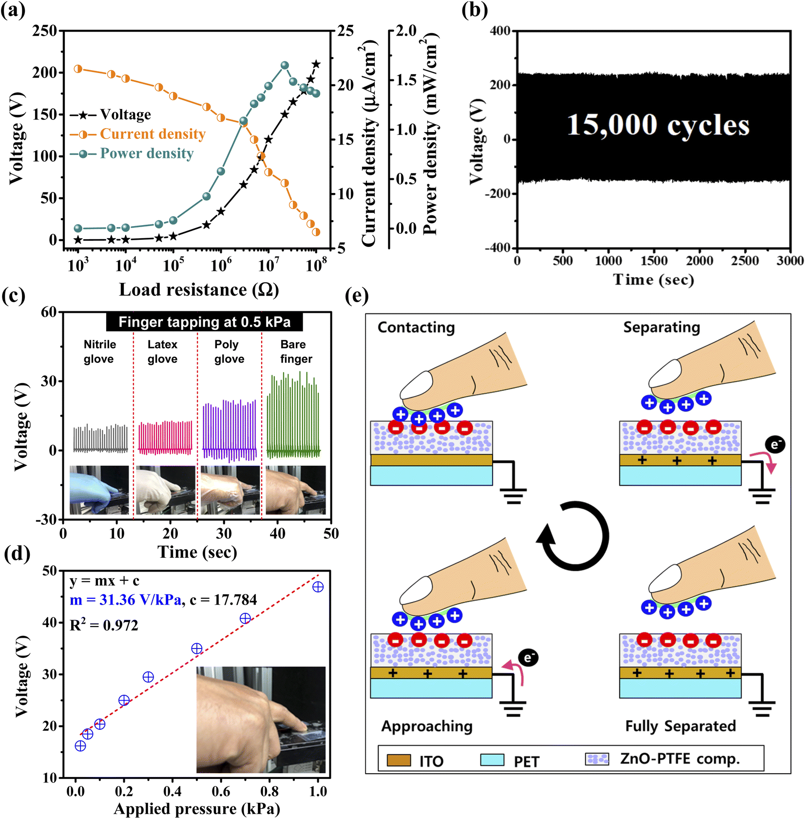
The effect of film thickness on the triboelectric output performance of the ZP-60 TENG under a constant applied pressure of 10 kPa is demonstrated in Fig. 4d and e. Here, the output performance is seen to increase gradually as the ZnO–PTFE film thickness is increased from 30 nm to 150 nm, such that the 150 nm thick ZP-60 TENG generates a high Voc of ∼224 V and a Jsc of ∼21.4 μA cm−2. In addition, the triboelectric output performance of 300 nm thick ZP-60 films was measured under similar conditions and a slightly increased triboelectric output performance was realized with a Voc of ∼244 V and Jsc of ∼24 μA cm−2 (Fig. S15a†). However, the transmittance was significantly decreased from 82.7% to 71.41% with the thickness of ZP-60 films increasing from 150 nm to 300 nm (Fig. S15b†). Therefore, the ZP-60 film thickness was limited to 150 nm in the present study to achieve reasonable transmittance characteristics with high triboelectric output. The triboelectric performance of the 150 nm thick ZP-60 TENG under various applied pressures of 0.01–10 kPa is demonstrated in Fig. 4f and g. Here, the triboelectric performance is clearly seen to increase gradually with increased applied pressure. The pressure-dependent output voltages in Fig. 4f are used to estimate the pressure-sensing ability of the ZP-60 TENG in Fig. 4h. Here, the device exhibits two distinct characteristics depending on the applied pressure, with pressure sensitivity and linearity values of 75.2 V kPa−1 and 0.972 in the low-pressure region, as compared to 12.53 V kPa−1 and 0.96 in the high-pressure region. The reason for perceiving two distinct pressure sensing characteristics for the device is related to the effective contact area between the two frictional materials under distinct applied pressures. Under low applied pressures, the contact surface between ZnO–PTFE and its counter friction part (i.e., PET substrate) will be relatively smaller, resulting in the generation of a small amount of triboelectric charges and corresponding electrical output signals. However, in the case of high applied pressures, the effective contact area between ZnO–PTFE and PET becomes larger thus leading to generation of high output performances. Moreover, under applied high pressures, the mechanical deformation of the piezoelectric ZnO material will be larger, which contributes to the improvement of triboelectric outputs by the combined piezoelectric and triboelectric effects. Notably, the obtained pressure sensitivity is much larger than that of the previously reported nanogenerator-based PENG or TENG pressure sensors, as demonstrated in Fig. 4i and Table 3, thereby demonstrating the outstanding pressure sensing ability of the ZP-60 TENG-based pressure sensor proposed herein.33,36,63,66–68 An enhanced output power and mechanical durability are indispensable requirements for the practical applicability of a TENG. Hence, the output power density of the ZP-60 TENG is obtained from the output voltage and current density measurements under various loads of 1 kΩ to 100 MΩ in Fig. 5a, where the output voltages are seen to increase gradually, while the current decreases sharply with increasing load. From these results, calculation gives a maximum output power density of 1.65 mW cm−2 at 22 MΩ. Meanwhile, the superior mechanical robustness of the ZP-60 TENG under continuous contact-separation mode for more than 15![[thin space (1/6-em)]](https://www.rsc.org/images/entities/char_2009.gif) 000 cycles at an applied pressure of 10 kPa is indicated in Fig. 5b, where the TENG is seen to generate a stable output performance without any degradation.
000 cycles at an applied pressure of 10 kPa is indicated in Fig. 5b, where the TENG is seen to generate a stable output performance without any degradation.
| Sensing Material | Device structure | Mode of operation | Pressure range (kPa) | Pressure sensitivity (V kPa−1) | Ref |
|---|---|---|---|---|---|
| MAPbI3-PVDF | MAPbI3/Au IDE/SEBS//Al2O3–Al | TENG | 2–300 | 0.194 | 33 |
| Ag nanowires@PTFE (Ag NWs@PTFE) | PVDF/Graphene/Ag NWs@ PTFE//finger | Hybrid PENG-TENG | 0.5–50 | 0.092 | 36 |
| ZnAL:LDH–PVDF | PET/ITO/ZnAL:LDH-PVDF//PET/ITO | TENG | 0.25–5 | 13.07 | 63 |
| MXene | Cu/Mxene//human skin (or PET) | TENG | 0.3–1 | 2.35 | 66 |
| PVDF-TrFE | Au/PVDF-TrFE//PDMS | TENG | 0.05–5 | 0.104 | 67 |
| FEP | EVA/Ag//FEP/Ag | TENG | 0.5–40 | 18.98 | 68 |
| ZnO–PTFE | PET/ITO/ZnO–PTFE//PET | TENG (single electrode) | 0.01–10 | 75.2 | This work |
| PET/ITO/ZnO–PTFE//human finger | 0.02–1 | 31.36 (touch sensitivity) |
 | ||
| Fig. 5 The triboelectric performance and mechanical endurance of the TENG: (a) the load resistance-dependent output voltage, current density, and power density of the TENG based on a 150 nm thick ZP-60 film at a constant applied pressure of 10 kPa and a frequency 5 Hz; (b) the mechanical endurance under 15000 cycles at an applied pressure of 10 kPa and a frequency of 5 Hz; (c) the triboelectric output voltages of the ZP-60-based single-electrode TENG when tapped by the bare finger or by the finger wearing various kinds of glove (insets: photographic images taken during measurement); (d) the plot of applied pressure against voltage for the ZP-60 TENG-based tactile sensor, where the slope indicates the touch sensitivity; (e) a schematic depiction of the working mechanism of the ZnO–PTFE-based single-electrode TENG. | ||
3.5. Touch sensor features of the ZnO–PTFE composite films
The touch sensing application of the antibacterial ZnO–PTFE-based TENG is demonstrated by the output performance under a continuous pressure of 0.5 kPa applied using either a bare or gloved finger in Fig. 5c and S16.† In the case of the gloved finger, the triboelectric output performance of the ZP-60 TENG is clearly changed according to the type of glove, with the poly-gloved finger generating much higher triboelectric outputs than the latex or nitrile gloves. This is attributed to the more highly positive triboelectric nature of the poly-glove, which is made of a low-density polyethylene. However, the TENG exhibits a much higher output performance when touched by the bare finger, with a peak output voltage of 34.5 V and an output current of 3.3 μA. This is attributed to the even more strongly positive triboelectric nature of the human hand.69 Further, the touch sensing ability of the ZP-60 TENG is demonstrated under various pressures of 0.02–1.0 kPa, as applied by tapping with the bare finger in Fig. S17 and S18.† Here, the output is seen to increase linearly with the increased tapping force, giving a high output voltage of 44 V and an output current of 4.7 μA at an applied pressure of 1 kPa. The curve of output voltage against applied pressure is presented in Fig. 5d, where the slope gives a calculated touch sensitivity of ∼31.36 V kPa−1 with a good linearity of 0.97 (Table 3).The mechanical energy-harvesting mechanism of the ZnO–PTFE-based single-electrode TENG is schematically shown in Fig. 5e. Here, the active ZnO–PTFE composite film sputtered on the ITO/PET substrate acts as a triboelectrically negative friction layer, and the underlying ITO acts as an electrode. Meanwhile, the finger acts as a positive friction layer when used to apply the force to the active material. One end of the TENG is connected to the ground during the measurement. Initially, no electricity is generated by the device due to the absence of an electric potential at the electrode. When the finger comes into contact with the ZnO–PTFE surface with a tapping motion, charge transfer takes place between the two surfaces, thereby generating a highly positive triboelectric charge on the human skin and an equal amount of negative triboelectric charge on the surface of the ZnO–PTFE, due to the large difference in their electron affinities.70 When the finger begins to separate from the ZnO–PTFE surface, the produced triboelectric charges on that surface induce opposite charges on the ITO electrode via the electrostatic induction effect, which results in a strong electric potential difference between the electrode and the adjacent ground. To balance this potential difference, electrons flow from the ITO electrode to the ground via an external circuit, thereby generating a positive electrical output signal. However, when the finger is fully detached from the ZnO–PTFE surface, the electrical potentials reach the equilibrium state, and no net current flows through the external circuit. As the finger approaches the ZnO–PTFE surface again, the induced positive charges on the electrode decrease, and the electrons flow from the ground to the electrode until both surfaces are in full contact with each other again. This results in an electrical output signal with an opposite polarity. Moreover, the output performance of a TENG will be enhanced if the TENG involves a good piezoelectric active material like ZnO,71 due to the combined effects of piezoelectric and triboelectric properties.72 When a piezoelectric material experiences mechanical deformation under an applied strain, the dipoles will be formed and the orientation of these dipoles will be significantly improved owing to the presence of the triboelectric electric field leading to enhancement in dipolar polarization which improves the generation of more negative charges on the surface of the ZnO–PTFE composite film during the operation of the TENG. In addition, the interfacial polarization near the interfaces of two heterostructures like ZnO and PTFE improves the surface charge density during TENG operation, allowing more electrons to move via the external load leading to enhancement in electric output performances.
3.6. Functional demonstration of ZnO–PTFE coatings
To demonstrate the practical applicability of the transparent ZnO–PTFE film as a display coating, a 30 nm thick ZP-60 composite film was deposited onto the commercially available tempered glass screen protector (half area) and the transmission characteristics of the screen protector without and with the ZnO–PTFE coatings were measured. As shown in Fig. 6a, the screen protector without ZnO–PTFE coatings displays a transmittance of ∼89.33% at 550 nm, while the ZnO–PTFE coated screen protector shows a nominal decline with a transmittance value of ∼86.06%. Further, the same ZnO–PTFE coated screen protector was attached to a smart phone screen and the touch-screen function test was conducted. No substantial changes in smart phone color and brightness were observed in uncoated (marked in yellow color at the top) and ZnO–PTFE coated (marked in red color at the bottom) parts of the screen (Fig. 6b) as evidenced by the earlier mentioned UV-transmittance values (Fig. 6a). More importantly, the touch-screen operation was still retained with the ZnO–PTFE coating (Fig. 6c, and video S1†). In addition, the touch-screen operation on a digital door lock system with bare hands was still retained with the ZnO–PTFE coating (Fig. 6d, and video S2†). These functional demonstrations clearly indicate the potential feasibility of antimicrobial ZnO–PTFE coatings for touchscreen application. | ||
| Fig. 6 Functional demonstration of ZnO–PTFE films: (a) UV-Vis transmittance spectra of the tempered glass screen protector without and with the ZP-60 coating. (b) ZP-60 coated-tempered glass screen protector attached onto a smart phone, (c) touch-screen functional test of a smart phone with the ZP-60 coated screen protector, and (d) touch-screen functional test of a digital door lock with ZP-60 coated PET. (e) Charging behavior of various capacitors charged by the output generated from the ZP-60 TENG under hand tapping, (f) powering of a calculator by the charged 4.7 μF capacitor, and (g) instant powering of 20 commercial green LEDs using generated output power from a ZP-60 TENG under hand tapping. | ||
Furthermore, to demonstrate the further practicability of ZnO–PTFE composite films, the ZP-60 TENG with an optimized thickness of 150 nm was used to harvest the biomechanical energy from hand tapping and the generated output was utilized to charge various capacitors of 0.22 μF, 2.2 μF, and 4.7 μF. The corresponding charging behavior of the capacitors along with the captured image of the capacitor changing during hand tapping on the TENG is illustrated in Fig. 6e. In which, the ZP-60 TENG is capable of charging a 4.7 μF capacitor up to ∼4.2 V in 70 s. Further, the charged 4.7 μF capacitor by the TENG was used to power the calculator (Fig. 6f) and the capacitor successfully turned on the calculator (video S3†). In addition, the ZP-60 TENG was connected to a set of commercial green light-emitting diodes (LEDs) and the generated power from the TENG under hand tapping was sufficient to directly turn on 20 green LEDs without the need for a storage device (Fig. 6g and video S4†), which proves the great potentiality of ZnO–PTFE composite films for mechanical energy harvesting application. All these findings unambiguously signify the great potentiality of sputtered ZnO–PTFE composite films as excellent surface coatings and self-powered touch sensors for wider applications in interactive touch devices.
4. Conclusions
Herein eco-friendly, flexible ZnO–PTFE composite thin films were fabricated for application in anti-reflective, antimicrobial touch-screen coatings and nanogenerator-based self-powered touch sensors. The amounts of PTFE in the ZnO–PTFE thin films were varied by RF co-sputtering under various applied powers. The PTFE polymer was shown to improve the hydrophobic and anti-reflectance properties of the ZnO film, as well as significantly enhancing the triboelectric output performance and providing high antibacterial activity against E. coli and S. aureus. The flexible ZnO–PTFE composite-based TENG demonstrated a triboelectric output voltage of ∼224 V, a current density of ∼21.4 μA cm−2, and a power density of 1.65 mW cm−2 at a low applied pressure of 10 kPa. Further, the TENG-based self-powered pressure sensor exhibited a superior pressure sensitivity of 75.2 V kPa−1, and a touch sensitivity of 31.36 V kPa−1, under applied pressures of 0.01 to 1.0 kPa, along with good mechanical durability and long-term operational stability. In addition, the functional application of ZnO–PTFE films as display coatings and self-powered touch sensors is demonstrated. These excellent antibacterial, anti-reflectance, and hydrophobic properties make the as-developed ZnO–PTFE thin films suitable for application as multi-functional surface coatings for touch panel displays and tactile sensors.Author contributions
Swathi Ippili: conceptualization, methodology, investigation, validation, funding acquisition, supervision, writing–original draft, writing–review & editing. Venkatraju Jella: conceptualization, methodology, validation, investigation, funding acquisition, supervision, writing–original draft, writing–review & editing, supervision. jeong min lee: investigation, assisted with experiments. Jang-Su Jung: investigation. Dong-Hyun Lee: investigation, Assisted with experiments. Tae-Youl Yang: investigation, validation. Soon-Gil Yoon: Conceptualization, methodology, validation, resources, investigation, project administration, writing–original draft, writing–review & editing, funding acquisition, supervision.Conflicts of interest
There are no conflicts of interests to declare.Acknowledgements
This work was supported by the National Research Foundation of Korea (NRF) grant funded by the Korean government (MSIP) (NRF-2021R1A2B5B03002016, NRF-2021R1A2C1010797, and NRF-2021R1I1A1A01060012) and by the Basic Research Program through the National Research Foundation of Korea (NRF) funded by the Ministry of Education (Grant No. 2021R1A6A1A03043682).References
- D. M. Morens and A. S. Fauci, PLoS Pathog., 2013, 9, e1003467 CrossRef CAS.
- R. E. Baker, A. S. Mahmud, I. F. Miller, M. Rajeev, F. Rasambainarivo, B. L. Rice, S. Takahashi, A. J. Tatem, C. E. Wagner, L.-F. Wang, A. Wesolowski and C. J. E. Metcalf, Nat. Rev. Microbiol., 2022, 20, 193 CrossRef CAS PubMed.
- N. Bhardwaj, M. Khatri, S. K. Bhardwaj, C. Sonne, A. Deep and K. H. Kim, Environ. Res., 2020, 186, 109569 CrossRef CAS PubMed.
- I. Kotris, D. Drenjančević, J. Talapko and S. Bukovski, Med. Glas., 2017, 14, 85 Search PubMed.
- A. Bhoonderowa, S. Gookool and S. Biranjia-Hurdoyal, J. Community Health, 2014, 39, 965 CrossRef CAS.
- W. Deng, Y. Sun, X. Yao, K. Subramanian, C. Ling, H. Wang, S. S. Chopra, B. B. Xu, J.-X. Wang, J.-F. Chen, D. Wang, H. Amancio, S. Pramana, R. Ye and S. Wang, Adv. Sci., 2022, 9, 2102189 CrossRef CAS.
- J. Barker, I. B. Vipond and S. F. Bloomfield, J. Hosp. Infect., 2004, 58, 42 CrossRef CAS.
- A. Bhalla, N. J. Pultz, D. M. Gries, A. J. Ray, E. C. Eckstein, D. C. Aron and C. J. Donskey, Infect. Control Hosp. Epidemiol., 2004, 25, 164 CrossRef PubMed.
- R. M. de Oliveira, N. M. da Rosa Gioppo, J. O. de Carvalho, F. C. Oliveira, T. J. Webster, F. R. Marciano and A. O. Lobo, Front. Chem. Sci. Eng., 2019, 13, 192 CrossRef CAS.
- O. Salata, J. Nanobiotechnol., 2004, 2, 3 CrossRef.
- H.-J. Choi, J.-S. Choi, B.-J. Park, J.-H. Eom, S.-Y. Heo, M.-W. Jung, K.-S. An and S.-G. Yoon, Sci. Rep., 2014, 4, 6271 CrossRef CAS PubMed.
- N. Jones, B. Ray, K. T. Ranjit and A. C. Manna, FEMS Microbiol. Lett., 2008, 279, 71 CrossRef CAS PubMed.
- V. Puspasari, A. Ridhova, A. Hermawan, M. I. Amal and M. M. Khan, ZnO-based antimicrobial coatings for biomedical applications, Bioprocess Biosyst. Eng., 2022, 45, 1421 CrossRef CAS.
- A. Rahman, M. H. Harunsani, A. L. Tan and M. M. Khan, Bioprocess Biosyst. Eng., 2021, 44, 1333 CrossRef CAS.
- A. Rahman, A. L. Tan, M. H. Harunsani, N. Ahmad, M. Hojamberdiev and M. M. Khan, J. Environ. Chem. Eng., 2021, 9, 105481 CrossRef CAS.
- A. Rahman, M. H. Harunsani, A. L. Tan, N. Ahmad, B. K. Min and M. M. Khan, Mater. Sci. Semicond. Process., 2021, 128, 105761 CrossRef CAS.
- A. Rahman, M. H. Harunsani, A. L. Tan, N. Ahmad and M. M. Khan, Chem. Pap., 2021, 75, 3295 CrossRef CAS.
- M. Hosseini, S. Behzadinasab, A. W. H. Chin, L. L. M. Poon and W. A. Ducker, ACS Biomater. Sci. Eng., 2021, 7, 5022–5027 CrossRef CAS PubMed.
- M. Arshad, A. Qayyum, G. A. Shar, G. A. Soomro, A. Nazir, B. Munir and M. Iqbal, J. Photochem. Photobiol., B, 2018, 185, 176 CrossRef CAS PubMed.
- H.-J. Choi, B.-J. Park, J.-H. Eom, M.-J. Choi and S.-G. Yoon, ACS Appl. Mater. Interfaces, 2016, 8, 997 CrossRef CAS PubMed.
- X. Zhang, L. Wang and E. Levänen, RSC Adv., 2013, 3, 12003 RSC.
- H. J. Choi, S. V. N. Pammi, B. J. Park, J. H. Eom, H. An, H. Y. Kim, M. Kim, D. Seol, Y. Kim and S. G. Yoon, J. Alloy. Compd., 2017, 719, 271 CrossRef CAS.
- S. Zhang, X. Liang, G. M. Gadd and Q. Zhao, Appl. Surf. Sci., 2019, 490, 231 CrossRef CAS.
- K. Yamauchi, Y. Yao, T. Ochiai, M. Sakai, Y. Kubota and G. Yamauchi, J. Nanotechnol., 2011, 1, 380979 Search PubMed.
- S.-Y. Heo, H.-J. Choi, B.-J. Park, J.-H. Um, H.-J. Jung, J.-R. Jeong and S.-G. Yoon, Sens. Actuators, A, 2015, 221, 131 CrossRef CAS.
- S. Ippili, B. Kim, V. Jella, J.-S. Jang, V.-H. Vuong and S.-G. Yoon, ACS Sustainable Chem. Eng., 2022, 10, 2136 CrossRef CAS.
- A. D. Valentine, T. A. Busbee, J. W. Boley, J. R. Raney, A. Chortos, A. Kotikian, J. D. Berrigan, M. F. Durstock and J. A. Lewis, Adv. Mater., 2017, 29, 1703817 CrossRef.
- V. Jella, S. Ippili, J. H. Eom, Y. J. Kim, H. J. Kim and S.-G. Yoon, Nano Energy, 2018, 52, 11 CrossRef CAS.
- V. Jella, S. Ippili, J. H. Eom, J. Choi and S.-G. Yoon, Nano Energy, 2018, 53, 46 CrossRef CAS.
- V. Jella, S. Ippili, J. H. Eom, S. V. N. Pammi, J. S. Jung, V. D. Tran, V. H. Nguyen, A. Kirakosyan, S. Yun, D. Kim, M. R. Sihn, J. Choi, Y. J. Kim, H. J. Kim and S. G. Yoon, Nano Energy, 2019, 57, 74 CrossRef CAS.
- M.-J. Choi, J.-H. Eom, S.-H. Shin, J. Nah, J.-S. Choi, H.-A. Song, H. An, H. Y. Kim, S. V. N. Pammi, G. Choi, J.-H. Choy, I. Swathi, V. Jella, B.-J. Park, J. Choi and S.-G. Yoon, Mater. Today Energy, 2018, 10, 254 CrossRef.
- S. Ippili, V. Jella, A. M. Thomas and S.-G. Yoon, Nanoenergy Adv., 2021, 1, 3 CrossRef.
- S. Ippili, V. Jella, S. Eom, S. Hong and S.-G. Yoon, ACS Appl. Mater. Interfaces, 2020, 12, 50472 CrossRef CAS PubMed.
- Y. W. Cai, X. N. Zhang, G. G. Wang, G. Z. Li, D. Q. Zhao, N. Sun, F. Li, H. Zhang, J. Han and Y. Yang, Nano Energy, 2021, 81, 105663 CrossRef CAS.
- G. Q. Gu, C. B. Han, J. J. Tian, C. X. Lu, C. He, T. Jiang, Z. Li and Z. L. Wang, ACS Appl. Mater. Interfaces, 2017, 9, 11882 CrossRef CAS.
- M. Ma, Z. Zhang, Z. Zhao, Q. Liao, Z. Kang, F. Gao, X. Zhao and Y. Zhang, Nano Energy, 2019, 66, 104105 CrossRef CAS.
- X. Peng, K. Dong, C. Ye, Y. Jiang, S. Zhai, R. Cheng, D. Liu, X. Gao, J. Wang and Z. L. Wang, Sci. Adv., 2020, 6, eaba9624 CrossRef CAS PubMed.
- S. Ippili, V. Jella, J. Kim, S. Hong and S.-G. Yoon, Nano Energy, 2018, 49, 247 CrossRef CAS.
- S. Ippili, V. Jella, J.-H. Eom, J. Kim, S. Hong, J.-S. Choi, V.-D. Tran, N. V. Hieu, Y.-J. Kim, H.-J. Kim and S.-G. Yoon, Nano Energy, 2019, 57, 911 CrossRef CAS.
- S. Ippili, V. Jella, J. Kim, S. Hong and S.-G. Yoon, ACS Appl. Mater. Interfaces, 2020, 12, 16469 CrossRef CAS PubMed.
- V. Jella, S. Ippili and S.-G. Yoon, ACS Appl. Electron. Mater., 2020, 2, 2579 CrossRef CAS.
- K. Hiroki, Antibacterial Products-Test for Antibacterial Activity and Efficacy; JIS Z 2801, Japanese Standards Association, Japan, 2000 Search PubMed.
- E. Cho, S. H. Kim, M. Kim, J.-S. Park and S.-J. Lee, Surf. Coat. Technol., 2019, 370, 18–23 CrossRef CAS.
- G. Z. Tang, X. X. Ma, M. R. Sun and X. D. Li, Carbon, 2005, 43, 345–350 CrossRef CAS.
- F. Alharthi, A. Alghamdi, N. Al-Zaqri, H. Alanazi, A. Alsyahi, A. El Marghany and N. Ahmad, Sci. Rep., 2020, 10, 20229 CrossRef CAS PubMed.
- E. H. Wolf, M.-M. Millet, F. Seitz, F. A. Redeker, W. Riedel, G. Scholz, W. Hetaba, D. Teschner, S. Wrabetz, F. Girgsdies, A. Klyushin, T. Risse, S. Riedel and E. Frei, Phys. Chem. Chem. Phys., 2020, 22, 11273 RSC.
- B. H. Park, M.-H. Lee, S. B. Kim and Y. M. Jo, Appl. Surf. Sci., 2011, 257, 3709 CrossRef CAS.
- S. Narasimman, L. Balakrishnan and Z. C. Alex, RSC Adv., 2018, 8, 18243 RSC.
- L. Cao, D. Li, T. Pollard, T. Deng, B. Zhang, C. Yang, L. Chen, J. Vatamanu, E. Hu, M. J. Hourwitz, L. Ma, M. Ding, Q. Li, S. Hou, K. Gaskell, J. T. Fourkas, X. Q. Yang, K. Xu, O. Borodin and C. Wang, Nat. Nanotechnol., 2021, 16, 902 CrossRef CAS PubMed.
- J. Chang, Z. Lin, M. Lin, C. Zhu, J. Zhang and J. Wu, J. Mater. Chem. C, 2015, 3, 1787 RSC.
- Y. Yang, X. W. Sun, B. J. Chen, C. X. Xu, T. P. Chen, C. Q. Sun, B. K. Tay and Z. Sun, Thin Solid Films, 2006, 510, 95 CrossRef CAS.
- S. B. Khan, H. Wu, Z. Xie, W. Wang and Z. Zhang, ACS Appl. Mater. Interfaces, 2017, 9, 36327 CrossRef CAS PubMed.
- E. F. Schubert, J. K. Kim and J. Q. Xi, Phys. Status Solidi B, 2007, 244, 3002 CrossRef CAS.
- R. Shannon, R. C. Shannon, O. Medenbach and R. X. Fischer, J. Phys. Chem., 2002, 31, 931 CAS.
- D. Fang, B. Yan, S. Agarwal, W. Xu, Q. Zhang, S. He and H. Hou, J. Mater. Sci., 2021, 56, 9344 CrossRef CAS.
- T.-C. Xu, C.-S. wang, Z.-Y. Hu, J.-J. Zheng, S.-H. Jiang, S.-J. He and H.-Q. Hou, Chinese J. Polym. Sci., 2022, 40, 764 CrossRef CAS.
- R. Mardosaitė, A. Jurkevičiūtė and S. Račkauskas, Cryst. Growth Des., 2021, 21, 4765 CrossRef.
- B. Deeksha, V. Sadanand, N. Hariram and A. V. Rajulu, J. Bioresour. Bioprod., 2021, 6, 75 CrossRef CAS.
- K. Yorseng, S. Siengchin, B. Ashok and A. V. Rajulu, J. Bioresour. Bioprod., 2020, 5, 101 CrossRef CAS.
- J. H. Choi, S.-Y. Seo, J.-S. Jung and S.-G. Yoon, ACS Appl. Electron. Mater., 2021, 3, 1429 CrossRef.
- H. Zou, L. Guo, H. Xue, Y. Zhang, X. Shen, X. Liu, P. Wang, X. He, G. Dai, P. Jiang, H. Zheng, B. Zhang, C. Xu and Z. L. Wang, Nat. Commun., 2020, 11, 2093 CrossRef CAS PubMed.
- Y. J. Kim, J. Lee, S. Park, C. Park, C. Park and H. J. Choi, RSC Adv., 2017, 7, 49368 RSC.
- S. Ippili, V. Jella, A. M. Thomas, C. Yoon, J.-S. Jung and S.-G. Yoon, J. Mater. Chem. A, 2021, 9, 15993 RSC.
- M. Á. Molina-García, Z. Sofer, J. K. Panda, m. Serri, M. Salerno, S. Marras, S. Lauciello, J. Plutnar and F. Bonaccorso, 2D Mater., 2022, 9, 044001 CrossRef.
- M. P. Kim, Y. Lee, Y. H. Hur, J. Park, J. Kim, Y. Lee, C. W. Ahn, S. W. Song, Y. S. Jung and H. Ko, Nano Energy, 2018, 53, 37 CrossRef CAS.
- Y. L. Cao, Y. B. Guo, Z. X. Chen, W. F. Yang, K. R. Li, X. Y. He and J. M. Li, Nano Energy, 2022, 92, 106689 CrossRef CAS.
- K. Parida, V. Bhavanasi, V. Kumar, R. Bendi and P. S. Lee, Nano Res., 2017, 10, 3557 CrossRef CAS.
- S. Chen, N. Wu, L. Ma, S. Lin, F. Yuan, Z. Xu, W. Li, B. Wang and J. Zhou, ACS Appl. Mater. Interfaces, 2018, 10, 3660 CrossRef CAS PubMed.
- R. Zhang, M. Hummelgård, J. Örtegren, M. Olsen, H. Andersson, Y. Yang, H. Zheng and H. Olin, Nano Energy, 2021, 86, 106041 CrossRef CAS.
- S. A. Shankaregowda, R. Ahmed, C. B. Nanjegowda, J. W. Wang, S. R. Guan, M. Puttaswamy, A. Amini, Y. L. Zhang, D. J. Kong, K. Sannathammegowda, F. Wang and C. Cheng, Nano Energy, 2019, 66, 104141 CrossRef.
- C. Yoon, S. Ippili, V. Jella, A. M. Thomas, J. S. Jung, Y. Han, T. Y. Yang, S.-G. Yoon and G. Yoon, Nano Energy, 2022, 91, 106691 CrossRef CAS.
- S. Ippili, V. Jella, J. Kim, S. Hong, H.-S. Kim and S.-G. Yoon, Nano Energy, 2022, 103, 107781 CrossRef CAS.
Footnote |
| † Electronic supplementary information (ESI) available. See https://doi.org/10.1039/d2ta06095g |
| This journal is © The Royal Society of Chemistry 2022 |