
 Open Access Article
 This Open Access Article is licensed under a
 Creative Commons Attribution 3.0 Unported Licence
Electronic structure of 2D hybrid perovskites: Rashba spin–orbit coupling and impact of interlayer spacing†
Meysam
Pazoki‡
 ab,
Roghayeh
Imani‡
c,
Andreas
Röckert
c and
Tomas
Edvinsson
*a
ab,
Roghayeh
Imani‡
c,
Andreas
Röckert
c and
Tomas
Edvinsson
*a
aDepartment of Materials Science and Engineering, Solid State Physics, Ångström Laboratory, Uppsala University, Box 34, 75121 Uppsala, Sweden. E-mail: tomas.edvinsson@angstrom.uu.se
bDepartment of Physics, Shiraz University, Shiraz 71454, Iran
cDepartment of Chemistry, Structural Chemistry, Ångström Laboratory, Uppsala University, Box 538, 75121, Uppsala, Sweden
First published on 8th September 2022
Abstract
Two-dimensional (2D) lead perovskite materials are of interest and under investigation in the solar cell and light-emitting device research community stemming from their high stability and intriguing anisotropic properties. Here we report electronic properties with and without spin–orbit coupling (SOC) together with the influence of van der Waals interaction. Particular attention is given to Rashba SOC, anisotropic band structure effects, and the impact of the electronic structure as a function of interlayer spacing with successively longer organic cations. The results show that larger cations, with a series from butyl-, hexyl-, octyl-, and decyl-diammonium, decrease the electrostatic interaction between the PbI4 planes in the 2D layered perovskites. SOC splitting of the conduction band states lowers the bandgap from 2.21 eV to 1.43 eV in the butyl-diammonium layered perovskite and results in a bandgap of about 1.5 eV in the analogs with longer cation chains. The k-dependent SOC effects (Rashba and Dresselhaus SOC) in the 2D and 3D structures are smaller than the k-independent SOC and are compared to Rashba SOC in III–V semiconductors, SrTiO3, and other 2D hybrid perovskites with respect to symmetry and I–Pb–I angles. The symmetry of the p-orbitals and the bandgap shifts were utilized to perform an analysis of the SOC coupling parameter in the structures in comparison with relativistic effects of isolated Pb. We also report that spacing directly affects the curvature of the bands and the charge carrier mobility perpendicular to the inorganic planes and thus affects the directional charge transport in the 2D perovskite. A distance of 6 nm is the maximum length between the 2D layers to retain a similar effective mass of holes (3m0) in-plane as out-of-plane to allow effective hole charge carrier transport perpendicular to the inorganic layer.
Introduction
Lead metal halide perovskite (LHP) materials were first implemented in a liquid solar cell in 2009 with relatively modest efficiency.1 In 2012 LHP materials were first implemented in solid-state perovskite solar cell devices with more encouraging efficiencies and have since attracted considerable research interest.2 The state-of-the-art solid-state devices currently deliver a certified record power conversion efficiency (PCE) of 25.7%,3 which is higher PCE than those achieved with 30–40 years of endeavors in CIGS, CdTe, and amorphous/multi-crystalline silicon solar cell technologies. The LHPs allow for bandgap tuning and thus have the advantage of optimizing spectral matching with adjacent materials in tandem configurations; LHPs together with silicon have shown certified efficiencies beyond 29.5%.3,4 The material class has also gained attention from a more fundamental point of view, showing phenomena from polarizability domains,5 Stark effect,6 large photo-induced dielectric constant,7 switchable photovoltaic effect,8 and slow hole cooling effects9 which considered in part as reasons of high performance of the perovskite devices. In addition, due to the presence of heavy elements such as Pb, there are large spin–orbit coupling (SOC) effects in the LHPs.10–12 In contrast to the typical small SOC split in valence band (VB) in conventional III–V semiconductors,13 there is instead a pronounced SOC split in the conduction band (CB) of LHPs14 affecting the bandgap and properties related to the nature of these new states as well as the device performance.The principal member of the perovskite solar cell family is CH3NH3PbI3 (methylammonium lead iodide-MAPbI3), in which MA monovalent cation does not play a direct role in the light absorption and have no contribution in top valence or bottom conduction band states; however, it can through steric/geometric effects affect the bandgap.15,16 Apart from affecting the band gap, the A-site cation plays a vital role for the defect formation energy17 and the ability for ion migration17,18 where a photoinduced thermalization mechanism has been suggested to be driving the effect under operation.6 These effects are subsequently important to understand electron–hole recombination properties in the systems.19 The main approach to theoretically estimate the bandgap and halide migration in metal halide perovskites has so far been DFT calculations based on GGA functionals. The leading reason is that the band dispersions at the valence and conduction band are similar to that of higher order approaches and that the common band gap underestimation using a GGA approach is absent for many of the lead perovskite materials. A large part of this comes from an error cancelation where neglecting of spin orbit coupling (SOC) and the absence of exact exchange in modelling of lead halide-based perovskite materials give theoretical band gaps very close to experimental data. For lead perovskites, inclusion of spin orbit coupling (SOC) will decrease the bandgap, while hybrid functionals or the GW-approximation will overestimate the band gap. GW calculations that include SOC effects instead result in a theoretical band gap again closer to the experimental values as in the case with GGA,16 which supports an underlying error cancelation. In addition, bulkier cations that cannot fit in the three-dimensional structure, according to Goldschmidt rules,20 can, however, enforce the formation of a layered perovskite structure. The emergence of two-dimensional (2D) lead iodide perovskite structures resulted in great improvements in the stability of perovskites and also a lower current–voltage hysteresis, keeping the device PCE and the hybrid perovskite material more stable.21 The hybrid structures are formally three-dimensional but consist of two-dimensional perovskite-structured layers interleaved between the organic cations and are related to Ruddlesden–Popper phases, but are in many sources just referred to as 2D hybrid perovskites. Due to the lower density of polarizable electrons per volume and the lower dielectric constants, they typically have lower optical absorption coefficients and stronger exciton binding energies than their 3D analogues.22,23 In addition, the 2D layered LHPs have been reported to have a large Rashba SOC splitting due to the broken symmetry in between the layers and the presence of the long organic chains.11,24 Therefore, understanding the nature of these organic chains and the corresponding impacts on the Rashba effect, conventional SOC, and electronic structure can be crucial for further engineering of hybrid layered perovskite solar cell materials and devices. Based on our previous research on 2D hybrid perovskites,25 we here investigate their Rashba SOC coupling, the influence of van der Waals (vdW) interaction, and the inter-layer spacing effects on the electronic structure of the materials. Typical alkyl di-ammonium cations (i.e., butyl, hexyl, octyl, and decyl di-ammonium) and the corresponding layered perovskite structures (abbreviated BDAPbI4, HDAPbI4, ODAPbI4, and DDAPbI4) with the three-dimensional counterpart (MAPbI3) depicted in Fig. 1 will be further investigated and compared in this work.
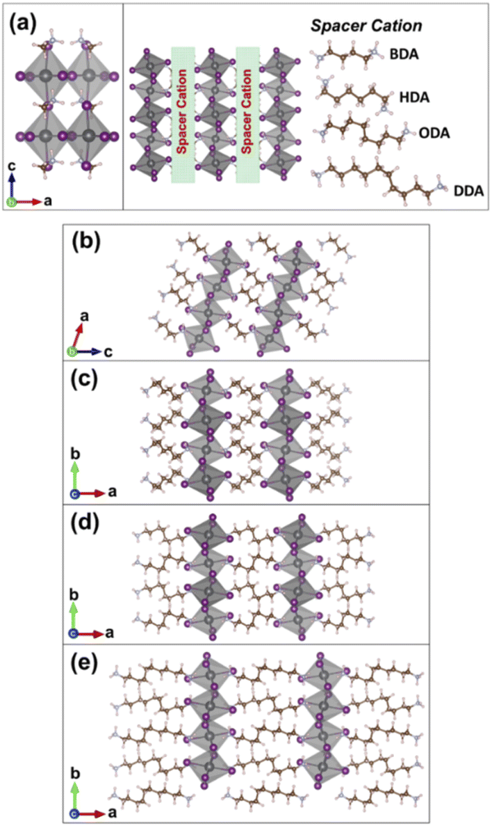 | ||
| Fig. 1 Unit cells for three-dimensional (a) MAPbI3, and a schematic illustration of the different spacer cations in between the inorganic layers in the two-dimensional perovskites of (b) BDAPbI4, (c) HDAPbI4, (d) ODAPbI4, and (e) DDAPbI4. The layered perovskites are shown in a two-unit cell scheme. Lead, iodide, carbon, nitrogen, and hydrogen atoms are represented by grey, purple, brown, blue, and pink spheres, respectively. | ||
Theoretical models and methods
All theoretical calculations were performed using the Quantum Espresso package26 according to previously reported procedures for lead perovskites.6,17,23,25 In summary, a plane wave (PW) basis set was utilized together with the PBE (Perdew–Burke–Ernzerhof) exchange–correlation functional. The starting configurations of the unit cells for the two-dimensional perovskites in the present study were based on experimental XRD data,27 unit-cell vectors and atom coordinates were optimized to have a force lower than 0.04 Ry/a.u. The reciprocal space was sampled using 2 × 4 × 4 Monkhorst–Pack grids in the 3D and 2D layered structures. The lead 5d10/6s2/6p2, the nitrogen 2s2/2p3, the iodide 5s2/5p5, and the carbon 2s2/2p2 electrons were considered as valence electrons. Three series of calculations based on different levels of theory were performed. The first included the generalized gradient approximation (GGA) functional PBE using Vanderbilt-type, scalar relativistic pseudopotentials. Cutoff energies of 35 and 350 Ry were used for the plane wave functions and the charge density, respectively. The second set was based on PBE–GGA and included SOC and projector augmented waves (paw) to describe the potentials; lead and iodide included fully relativistic effects, denoted SOC. The third set shared all computational parameters with the SOC set and included van der Waals (vdW) correction based on the semi-empirical approach with GGA, described by Grimme et al.28 and is denoted SOC–London. The latter two approaches used cutoffs of 100 and 800 Ry, respectively.The Xcrysden package29 and VESTA package30 were used to visualize the charge densities and unit cells. Effective masses were extracted by fitting the curvature of the energy dispersion near the band edges, as described in more detail in ref. 31. The obtained effective mass of the carriers implicitly assumes a harmonic dispersion and is extracted viaeqn (1) and (2), i.e., from the second derivative of energy versus crystal momentum:
 | (1) |
 | (2) |
Results and discussion
Geometrical factors
We analyse the structures by providing a description of the lattice vectors, average bond lengths, octahedral tilting, and spacing between the inorganic layers for different levels of implemented theory as reported in Table 1. Further information about experimental crystal structures can be found in ref. 25 and 27. The lattice parameters of the relaxed structures are provided in Table S1 in ESI† based on SOC and relativistic effects for either lead or both lead and iodide.| Structure | Method | In-plane | Out-of-plane | ||
|---|---|---|---|---|---|
| Pb–I (Å) | <I–Pb–I (degree) | Pb–I (Å) | <I–Pb–I (degree) | ||
| BDAPbI4 | Scal relativistic | 3.27 | 179.89 | 3.24 | 179.73 |
| SOC | 3.27 | 179.87 | 3.25 | 179.66 | |
| SOC + London | 3.28 | 179.83 | 3.28 | 179.63 | |
![[thin space (1/6-em)]](https://www.rsc.org/images/entities/char_2009.gif) |
|||||
| HDAPbI4 | Scal relativistic | 3.21 | 179.94 | 3.18 | 179.96 |
| SOC | 3.24 | 179.98 | 3.21 | 179.98 | |
| SOC + London | 3.24 | 179.97 | 3.24 | 179.97 | |
|
|||||
| ODAPbI4 | Scal relativistic | 3.20 | 179.98 | 3.19 | 179.97 |
| SOC | 3.22 | 179.95 | 3.22 | 179.97 | |
| SOC + London | 3.23 | 179.94 | 3.23 | 179.96 | |
|
|||||
| DDAPbI4 | Scal relativistic | 3.26 | 178.17 | 3.24 | 178.25 |
| SOC | 3.26 | 177.98 | 3.24 | 178.25 | |
| SOC + London | 3.27 | 177.94 | 3.27 | 178.32 | |
|
|||||
| MAPbI3 | Scal relativistic | 3.21 | 177.39 | 3.18 | 169.99 |
| SOC | 3.21 | 176.99 | 3.18 | 169.98 | |
| SOC + London | 3.22 | 176.03 | 3.18 | 169.55 | |
Considering the calculated structures using the scalar relativistic, SOC, and SOC–London approach, the difference in bond lengths and angles within the inorganic layers are small (less than 0.2-degree difference in the bond angles and less than 0.1 Å in bond lengths within the Pb–I plane). The Pb–I bonds out of the plane, however, along the Z axis of the lattice, differ up to 0.4 Å in bond lengths when vdW correction is included. The BDA structure, with the shortest organic cation chain, showed the largest Pb–I bond length with 3.24 Å, a bond length that decreases with longer chained cations, pointing to interactions of organic spacers, as well as the interaction between the Pb–I layers up to a certain chain length. From the results for each structure, it is apparent that the inclusion of vdW forces and spin–orbit coupling both slightly increase the Pb–I bond length out of plane compared to the scalar relativistic calculations.
Bandgap values and effective mass of charges
The bandgap is usually considered as one of the key properties for photovoltaic materials, along with charge carrier mobility and defect tolerance. There is commonly an underestimation of the bandgap for conventional semiconductors by DFT GGA calculations which is a known issue. However, for three-dimensional MAPbI3 and similar structures there is an error cancelation where the theoretical calculations match the experimental bandgap quite well,32 but this is not the case for 2D perovskites. The absolute value of the experimental bandgap is not reproduced by the GGA functional but instead by hybrid functionals using more than 40% of Fock exchange contribution.25,33 A summary and comparison of the band gaps and structural parameters obtained in the present work are presented in Table 2 and ESI.† The data show no large difference in bandgap upon inclusion of vdW interaction, as also expected from the small influence of the in-plane structural Pb–I parameters for either scalar relativistic GGA or GGA with SOC. For the calculations based on the scalar relativistic potentials, the bandgap value lies between 2.15–2.3 eV for all the structures, while they change to 1.5 ± 0.1 eV using SOC. As apparent, the inclusion of SOC results in a sizable change of predicted band gaps and split of the CB states. This is expected for LHPs where Pb localized states dominate the CB edge and the iodide states dominate the VB edge, as also apparent from the PDOS (ESI, Fig. S1†). One can thus expect a significantly higher SOC split at the CB edge containing electronic states originating from elements with highest nuclei charge. One can also note a small change in dispersion for the lower CB edge, but a larger change for the upper CB edge dispersion.| Structure | Method | Bandgap [eV] | In-plane | Out-of-plane | ||
|---|---|---|---|---|---|---|
|
|
|
|
|
|||
| a The lack of dispersion for the VB for Γ → Z in BDAPbI4 made this value highly uncertain and is only presented here to show the numerical outcome. | ||||||
| BDAPbI4 | Scal relativistic | 2.21 | 2.41 | 2.64 | −1236.55a | 2.83 |
| SOC | 1.43 | 2.29 | 2.77 | 12.31 | 3.28 | |
| SOC + London | 1.43 | 2.34 | 2.80 | 11.06 | 2.97 | |
|
||||||
| HDAPbI4 | Scal relativistic | 2.15 | 9.23 | 16.81 | 19.71 | 70.77 |
| SOC | 1.50 | 8.88 | 17.26 | 21.34 | 54.25 | |
| SOC + London | 1.51 | 9.02 | 18.34 | 22.16 | 68.05 | |
|
||||||
| ODAPbI4 | Scal relativistic | 2.16 | 12.67 | 19.59 | 32.44 | 51.57 |
| SOC | 1.52 | 11.69 | 21.42 | 31.51 | 47.82 | |
| SOC + London | 1.53 | 11.88 | 23.05 | 31.46 | 49.25 | |
|
||||||
| DDAPbI4 | Scal relativistic | 2.32 | 10.64 | 15.42 | 48.58 | 56.70 |
| SOC | 1.54 | 9.72 | 17.60 | 64.42 | 103.90 | |
| SOC–London | 1.54 | 10.02 | 17.87 | 71.61 | 104.50 | |
|
||||||
| MAPbI3 | Scal relativistic | 1.57 | 5.35 | 1.78 | 0.80 | 1.45 |
| SOC | 0.67 | 1.79 | 1.69 | 0.97 | 1.25 | |
| SOC + London | 0.73 | 2.11 | 1.94 | 1.01 | 1.31 | |


The origin of the effect is a combination of an asymmetric crystal potential and the spin–orbit interaction, leading to a broken inversion symmetry in the crystal in the direction perpendicular to inorganic layers (z-axis). The calculated band structure, band gaps, density of states together with charge carrier effective masses derived from the bands are presented in Fig. 2–5 and Table 2. The observed trend for both electron and hole effective masses within the inorganic layer plane and out of plane is an increase in the effective mass of the charge carriers with  The hole effective masses are in general high and at the same order of magnitude for all the structures except for BDA with both in-plane
  and out-of-plane
  effective hole masses around 3m0. This is in contrast to the longer interlayer spacing's effective masses of the holes with 51–100m0 extracted for the out-of-plane direction (Table 2). The variation in effective masses with values above 50m0 should be taken with care, though, as the numerical error in fitting flat bands is high. The results underpin the potential for implementing 2D capping of BDA perovskites on top of 3D perovskites without a significant decrease of charge carrier mobility at the interface to the contact material. The interlayer distance in BDA is 6 nm; at this separation, dispersion is seen out-of-plane, and thus revealing that electronic interaction occurs in-between the layers. To keep similar hole effective masses out-of-plane as in-plane, that is 2.97m0vs. 2.80m0 (SOC + vdW, Γ–Z, Table 2), an organic spacer should not separate the layers more than approximately 6 nm. As this at the same time increase the electron effective mass by a factor 5, in comparison to the in-plane value, it forms an effective hole selective layer with more or less retained hole transfer properties.
 | ||
| Fig. 2 Calculated band structure of BDAPbI4 within: (a) GGA without SOC, core electrons represented by scalar-relativistic pseudopotentials, (b) GGA approximation with SOC, using projected augmented wave functions, (c) GGA approximation with SOC including London dispersion, using projected augmented wave functions. | ||
 | ||
| Fig. 3 Calculated band structure of HDAPbI4 within: (a) GGA approximation without SOC, core electrons represented by scalar-relativistic pseudopotentials, (b) GGA approximation with SOC, using projected augmented wave functions, (c) GGA approximation with SOC including London dispersion, using projected augmented wave functions. | ||
 | ||
| Fig. 4 Calculated band structure of ODAPbI4 within: (a) GGA approximation without SOC, core electrons represented by scalar-relativistic pseudopotentials, (b) GGA approximation with SOC, using projected augmented wave functions, (c) GGA approximation with SOC including London dispersion, using projected augmented wave functions. | ||
 | ||
| Fig. 5 Calculated band structure of DDAPbI4 within: (a) GGA approximation without SOC, core electrons represented by scalar-relativistic pseudopotentials, (b) GGA approximation with SOC, using projected augmented wave functions, (c) GGA approximation with SOC including London dispersion, using projected augmented wave functions. | ||
For the 2D structures with longer chain lengths, no or very small dispersion is observed in the out-of-plane direction. The largest distance at which the layers interact and improve the dispersion of the VB states out-of-plane is thus 6 nm (BDA, Fig. 2), resulting in an appreciable charge carrier mobility compared to other structures with longer cation chains and close to flat bands in the out-of-plane direction (Fig. 3–5). In-plane and out-of-plane effective masses for the charge carriers as extracted for the band curvature are summarized in Table 2. For more details on the effect of this on the spatial charge densities, see Fig. S6–S7 of ESI† in which the plotted charge densities show the interaction of out-of-plane iodine atoms with BDA cations in contrast to HDA, ODA, and DDA perovskites.
From the results above, there is substantial difference in the shift of the CB and VB states, as well as remaining dispersion out-of-plane for the 2D hybrid perovskites with plane inter-distance up to 6 nm for a retained effective charge carrier mass of the hole out-of-plane as in-plane (∼3m0). To analyses details of k-dependent SOC effects, as predicted by Sheka and Rashba in 1959 for Wurtzite crystals34,35 and similarly extracted for a 2D electron gas system by Bychkov years later.36 Following their approach, the k-dependent SOC Hamiltonian HSO can be written as:
| HSO = α(σ × k)ν | (3) |
 | (4) |
 | (5) |
| Structure | Method | k 0 [Å−1] | ΔE± [meV] | α eff [eV Å] |
|---|---|---|---|---|
| BDAPbI4 | Scal relativistic | 0.0117 | 0.0203 | — |
| SOC + London | 0.0100 | 0.0028 | 0.0001 | |
|
||||
| HDAPbI4 | Scal relativistic | 0.0068 | 0.0000 | — |
| SOC + London | 0.0068 | 0.0000 | 0.0000 | |
|
||||
| ODAPbI4 | Scal relativistic | 0.0085 | 0.0133 | — |
| SOC + London | 0.0068 | 0.0081 | 0.0006 | |
|
||||
| DDAPbI4 | Scal relativistic | 0.0237 | 0.3587 | — |
| SOC + London | 0.0356 | 0.7504 | 0.0105 | |
|
||||
| MAPbI3 | Scal relativistic | 0.0133 | 5.1283 | — |
| SOC + London | 0.0217 | 12.1757 | 0.2802 | |
The results show that all 2D structured perovskites, except the one with largest organic chain length, have negligible Rashba spin–orbit coupling compared to the reference (scalar relativistic) calculation (Table 3) and the main effect seen must instead be related to conventional SOC. This is in line with the recent results of negligible Rashba to very small effects (0.0–0.2 eV Å) seen for similar 2D hybrid perovskites using experimental local structure descriptors and similar I–Pb–I angles (up to 2° I–Pb–I angles, Table 1).37 For the cubic MAPbI3 the apparent Rashba effect is larger with αeff of 0.28 eV Å but is instead a Dresselhaus effect, related to the pseudo cubic systems as explained below. It is known that the MAPbI3 has low frequency phonons below 200 cm−1 (25 meV)38,39 that naturally are excited at room temperature. The experimentally determined X-ray structures for the cubic systems are thus time averaged structures for different displacements along these soft modes. The ab initio calculated structures optimized here at zero Kelvin, represents one of the configurations with the energy below the convergence threshold at low temperatures, and should be treated with care when comparing with the temperature averaged structure at room temperature. Although the use and results from a low temperature configuration in many cases reproduce experimental values and information of excited state properties,40 care has to be taken if dynamic properties are to be extracted that could be dependent on small structural changes along the soft modes. With this note of precaution, and using the theoretical structure as a representative structure of one of the lowest energy configurations in the room temperature averaged cubic structure, we proceed with the analysis. The k-dependent SOC split in the 3D MAPbI3 does not originate in a symmetry-axis perpendicular to a structure with 2D sub-symmetry as required for Rashba SOC and is instead related to the Dresselhaus SOC, relevant for zinc blende and other cubic crystal systems without a centre of inversion.41 The separation of Rashba and Dresselhaus k-dependent SOC split in non-centrosymmetric crystals is experimentally challenging for complex geometries with several sub-symmetries or polycrystalline films, while they can be separated via spin precession in oriented single crystals.42 Experimental results for oriented InAlAs/InGaAs2 and SrTiO3 crystals reveal Rashba coupling parameters, αeff, of 0.07 eV Å and 0.05 eV Å, respectively,42–44 and thus five times higher Rashba effect for SrTiO3 compared to the 2D perovskite DDAPbI4 of αeff of 0.01 eV Å (Table 3), while the Dresselhaus effect in the pseudo cubic MAPbI3, is instead higher in magnitude compared to the k-dependent Rashba shift reported for InAlAs/InGaAs2 and SrTiO3.
Using the aforementioned estimation of the Rashba effect in 2D hybrid perovskites, using local structure descriptors37 with octahedral tilting extracted from single crystal experimental structures for samples with different length and type of organic spacers, αeff falls in the range of 0.0 to 0.2 for in-plane and out-of-plane I–Pb–I bond angle disparity of up to 1.37
This is in good agreement with the results obtained from our ab initio calculations, showing more or less zero αeff for the I–Pb–I angle planes close to zero, and a slightly larger value for DDAPbI4 with a larger angle (Table 1). Apart from the k-dependent SOC effects (Rashba and Dresselhaus), there is also a larger conventional SOC effect as apparent in the splitting of CB states and markedly changed band gap upon inclusion of SOC in the calculations. The SOC Hamiltonian from a Schrödinger equation perspective can be written:45
 | (6) |
![[small klambda, Greek, circumflex]](https://www.rsc.org/images/entities/i_char_e11a.gif) is the SOC coupling parameter, L the angular moment operator, S the spin angular-momentum vector, and r the orbital radius from the central field approximation, in comparison with the classical result of
is the SOC coupling parameter, L the angular moment operator, S the spin angular-momentum vector, and r the orbital radius from the central field approximation, in comparison with the classical result of  where Lclassical is the angular momentum r × p. In the latter classical analogue, p is the classical momentum me × ν with the velocity ν of the electron. This implies that the magnetic field (and thus the SOC) is parallel to the orbital angular momentum and in turn perpendicular to the electron's velocity vector. The relativistically corrected HSOC using the Dirac equation is half the one in eqn (6).46,47 Although the numerical DFT calculations together with the relativistic corrected HSOC from the DFT calculations give the magnitude of the SOC shifts, it can be valuable to analyse them also from an analytic perspective to highlight symmetries and resulting degeneracy. Here one can consider a second order perturbation approach to the SOC following the Rayleigh–Schrödinger perturbation scheme.45
 | (7) |
If we now analyse the CB edge and the predominant 6p Pb orbitals, we can utilize that the local spin–orbit coupling in the local p orbitals are compatible to the lattice symmetry of the states as long as they have the same degeneracy,48 and consider the local symmetry for analysis. Lead(II) in the perovskite structures have the electronic structure [Xe] 6s2 4f14 5d10 6p0, assuming fully ionic bonds with lead present mainly as Pb2+, with 6p orbitals at the CB edge and the VB edge states dominated by the iodide 5p states and occupied Pb states further down in energy (PDOS, ESI, Fig. S1–S5†). Considering SOC as a perturbation and utilizing eqn (7), the first order perturbation with respect to pz is
 | (8) |
The total contribution would be 3 times eqn (8) for states extending also into px and py, assuming no sp-hybridization. The corresponding second order contribution is:
 | (9) |
The allowed orbital angular momentum (l) of the p orbitals, are −1, 0, and +1 with spin states of ms = ±½, and thus six states. Translating this to the corresponding HSOC matrix from eqn (6) with the states |1½>, |1 − ½>, |0½>, |0 − ½>, |−1½>, and |−1 − ½> and performing a diagonalization, we have the eigenvalues of 0.5 λ and −λ and thus a SOC intra band split amplitude of 1.5 λ, while the shift of the CB edge is −λ (Fig. 6).
 | ||
| Fig. 6 Schematic illustration of the effect of SOC interaction and the k-dependent Rashba effect on the CB 6p orbitals in the 2D lead halide perovskites. | ||
The upper states have a four-fold degeneracy and the states at the lower CB edge have a two-fold degeneracy. The downward split (−λ) can be related to the CB shift from the DFT calculations using SOC for e.g. BDAPbI4 of 0.78 eV (Table 2) and thus corresponding to λ of −0.78 eV from the analysis above. This can be compared to the SOC constant λ of −0.91 eV for elemental Pb.49
The corresponding CB shifts (−λ) of the other 2D perovskites are all in the range of 0.64 eV to 0.78 eV and indicate that the bonding to iodine in the hybrid Ruddlesden–Popper like 2D perovskite structure and phenomenological loss of 2 electrons for Pb and hybridization, upon bonding, results in a decrease of the SOC effects for the CB shift in the range of 0.13 eV to 0.27 eV, depending on the length of organic cation layer and distortion of the inorganic perovskite layer. The CB shift of 3D MAPbI3 and the corresponding SOC constant (λ = −0.90 eV) is instead similar as in elemental lead. The vdW interactions on the other hand, are only affecting the shift on the order of 0.01 eV for the 2D perovskites and is of similar amplitude as the broadened transition region (∼4 kT) of the conventional Fermi–Dirac distribution at non-zero temperatures.
Conclusions
Two-dimensional (Ruddlesden–Popper like) layered perovskite solar cell materials are of interest due to their high stability and utilization as interface layers in solar cell devices, but also from a fundamental physics perspective and their particular electronic structure. Organic cations with different lengths provide the possibility to tune the interlayer spacing between the inorganic layers. With successively longer carbon chains, here investigated as a series of 2D layered perovskites with butyl-, hexyl-, octyl-, and decyl-diammonium cations, one obtains tunable distances between the PbI4 planes. SOC splitting of the conduction band states was seen to lower the bandgap from 2.21 eV to 1.43 eV in the butyl-diammonium layered perovskite, resulting in a bandgap of about 1.5 eV in the 2D analogues with longer cation chains. Distances up to 6 nm in-between the 2D layers retain electronic interaction perpendicular to the inorganic 2D layers, creating a reasonably low effective mass of the holes (3m0) traversing the layers. This allows a similar charge carrier mobility as within the inorganic layer and allow appreciable charge carrier transport also perpendicular to the inorganic 2D layers. The result can thus rationalize and explain why only very thin 2D layers (up to 5 nm) are used for capping of 3D perovskites with retained device functionality as seen previously in trial-and-error from experimental efforts,50,51 while the more exact thickness will depend on potential inherent and thermally induced distortions in the structure. Analysis of the k-dependent Rashba effect in the proximity to the Γ-point, showed minor effects, in comparison to the k-dependent Dresselhaus split in the cubic 3D perovskite MAPbI3, with a SOC parameter one magnitude larger. The symmetry of the p-orbitals and band gap shifts were utilized to perform an analysis of the SOC coupling parameter λ in the structures in comparison to SOC coupling in Pb as an element. The results are in agreement with recent results extracted for experimentally determined structure effects for 2D perovskites, and here further analysed in term of the k-independent and k-dependent SOC coupling and effects related to the length of the organic cations and the I–Pb–I angle planes. The presented data and analysis show fundamental aspects of the layered 2D perovskites with successively longer inorganic layer distances, with and without SOC and vdW interaction, paving routes towards a better understanding of the interaction between lead iodide layers in 2D perovskite solar cell materials.Conflicts of interest
There are no conflicts to declare.Acknowledgements
We would like to thank Jolla Kullgren and Pavlin Mitev for helpful discussions on how to implement van der Waals corrections in Quantum Espresso. We acknowledge the Swedish energy agency for the financial support of this work through grant number 43294-1, 50667-1, and the Swedish research council grant number 2019-05591. MP acknowledges Iranian National Elite Foundation and Dr Abbas Ghasempour Adrdakani for the support of this work. This work made use of computational resources provided by the Swedish National Infrastructure for Computing (SNIC) under projects snic2017-1-158, snic2018-3-228, snic2019-1-34, and snic2020-5-294.References
- A. Kojima, K. Teshima, Y. Shirai and T. Miyasaka, J. Am. Chem. Soc., 2009, 131, 6050 CrossRef CAS PubMed.
- J. P. Correa-Baena, M. Saliba, T. Buonassisi, M. Grätzel, A. Abate, W. Tress and A. Hagfeldt, Science, 2017, 358, 739–744 CrossRef CAS.
- Nationl Cent. Photovoltaics, https://www.nrel.gov/pv/cell-efficiency.html.
- Z. Wang, X. Zhu, S. Zuo, M. Chen, C. Zhang, C. Wang, X. Ren, Z. Yang, Z. Liu, X. Xu, Q. Chang, S. Yang, F. Meng, Z. Liu, N. Yuan, J. Ding, S. Liu and D. Yang, Adv. Funct. Mater., 2020, 30, 1–8 Search PubMed.
- Y. Kutes, L. Ye, Y. Zhou, S. Pang, B. D. Huey and N. P. Padture, J. Phys. Chem. Lett., 2014, 5, 3335–3339 CrossRef CAS PubMed.
- M. Pazoki, T. J. Jacobsson, J. Kullgren, E. M. J. Johansson, A. Hagfeldt, G. Boschloo and T. Edvinsson, ACS Nano, 2017, 11, 2823–2834 CrossRef CAS PubMed.
- E. J. Juarez-Perez, R. S. Sanchez, L. Badia, G. Garcia-Belmonte, Y. S. Kang, I. Mora-Sero and J. Bisquert, J. Phys. Chem. Lett., 2014, 5, 2390–2394 CrossRef CAS PubMed.
- Z. Xiao, Y. Yuan, Y. Shao, Q. Wang, Q. Dong, C. Bi, P. Sharma, A. Gruverman and J. Huang, Nat. Mater., 2015, 14, 193–197 CrossRef CAS PubMed.
- Y. Yang, D. P. Ostrowski, R. M. France, K. Zhu, J. Van De Lagemaat, J. M. Luther and M. C. Beard, Nat. Photonics, 2016, 10, 53–59 CrossRef CAS.
- J. Even, L. Pedesseau and C. Katan, J. Phys. Chem. C, 2014, 118, 11566–11572 CrossRef CAS.
- J. Even, L. Pedesseau, M. a. Dupertuis, J. M. Jancu and C. Katan, Phys. Rev. B: Condens. Matter Mater. Phys., 2012, 86, 3–6 CrossRef.
- J. Even, L. Pedesseau, J. M. Jancu and C. Katan, J. Phys. Chem. Lett., 2013, 4, 2999–3005 CrossRef CAS.
- P. Y. Yu and M. Cardona, Fundamentals of Semiconductors, Springer, 1996 Search PubMed.
- C. Katan, L. Pedesseau, M. Kepenekian, A. Rolland and J. Even, J. Mater. Chem. A, 2015, 3, 9232–9240 RSC.
- M. R. Filip, G. E. Eperon, H. J. Snaith and F. Giustino, Nat. Commun., 2014, 5, 1–9 Search PubMed.
- M. Pazoki and T. Edvinsson, Sustainable Energy Fuels, 2018, 2, 1430–1445 RSC.
- M. Pazoki, M. J. Wolf, T. Edvinsson and J. Kullgren, Nano Energy, 2017, 38, 537–543 CrossRef CAS.
- C. J. Tong, W. Geng, O. V. Prezhdo and L. M. Liu, ACS Energy Lett., 2017, 2, 1997–2004 CrossRef CAS.
- C. J. Tong, X. Cai, A. Y. Zhu, L. M. Liu and O. V. Prezhdo, J. Am. Chem. Soc., 2022, 144, 6604–6612 CrossRef CAS PubMed.
- T. J. Jacobsson, M. Pazoki, A. Hagfeldt and T. Edvinsson, J. Phys. Chem. C, 2015, 119, 25673–25683 CrossRef CAS.
- A. A. Sutanto, N. Drigo, V. I. E. Queloz, I. Garcia-Benito, A. R. Kirmani, L. J. Richter, P. A. Schouwink, K. T. Cho, S. Paek, M. K. Nazeeruddin and G. Grancini, J. Mater. Chem. A, 2020, 8, 2343–2348 RSC.
- Characterization Techniques for Perovskite Solar Cell Materials, ed. M. Pazoki, A. Hagfeldt and T. Edvinsson, Elsevier, 1st edn, 2019 Search PubMed.
- M. Pazoki, T. J. Jacobsson, A. Hagfeldt, G. Boschloo and T. Edvinsson, Phys. Rev. B, 2016, 93, 1–10 CrossRef.
- Y. Zhai, S. Baniya, C. Zhang, J. Li, P. Haney, C. X. Sheng, E. Ehrenfreund and Z. V. Vardeny, Sci. Adv., 2017, 3, 1–7 Search PubMed.
- D. Phuyal, M. Safdari, M. Pazoki, P. Liu, B. Philippe, T. Edvinsson, K. O. Kvashnina, O. Karis, S. M. Butorin, L. Kloo and J. M. Gardner, Chem. Mater., 2018, 30, 4959–4967 CrossRef CAS.
- P. Giannozzi, S. Baroni, N. Bonini, M. Calandra, R. Car, C. Cavazzoni, D. Ceresoli, G. L. Chiarotti, M. Cococcioni, I. Dabo, A. Dal Corso, S. De Gironcoli, S. Fabris, G. Fratesi, R. Gebauer, U. Gerstmann, C. Gougoussis, A. Kokalj, M. Lazzeri, L. Martin-Samos, N. Marzari, F. Mauri, R. Mazzarello, S. Paolini, A. Pasquarello, L. Paulatto, C. Sbraccia, S. Scandolo, G. Sclauzero, A. P. Seitsonen, A. Smogunov, P. Umari and R. M. Wentzcovitch, J. Phys.: Condens. Matter, DOI: DOI:10.1088/0953-8984/21/39/395502.
- M. Safdari, A. Fischer, B. Xu, L. Kloo and J. M. Gardner, J. Mater. Chem. A, 2015, 3, 9201–9207 RSC.
- S. Grimme, T. O. Chemie and O. I. D. U. Münster, J. Comput. Chem., 2006, 16, 1787–1799 CrossRef.
- A. Kokalj, Comput. Mater. Sci., 2003, 28, 155–168 CrossRef CAS.
- K. Momma and F. Izumi, J. Appl. Crystallogr., 2011, 44, 1272–1276 CrossRef CAS.
- M. Pazoki, M. B. Johansson, H. Zhu, P. Broqvist, T. Edvinsson, G. Boschloo and E. M. J. Johansson, J. Phys. Chem. C, 2016, 120, 29039–29046 CrossRef CAS.
- P. Umari, E. Mosconi and F. De Angelis, Sci. Rep., 2014, 4, 1–7 Search PubMed.
- Z. Wang, A. M. Ganose, C. Niu and D. O. Scanlon, J. Mater. Chem. A, 2018, 6, 5652–5660 RSC.
- E. I. Rashba, Sov. Phys. Solid State, 1959, 1, 368–380 CAS.
- E. I. Rashba and V. I. Sheka, New J. Phys., 1959, 17, 62–76 Search PubMed.
- Y. A. Bychkov and E. I. Rashba, JETP Lett., 1984, 39, 78–81 Search PubMed.
- M. K. Jana, R. Song, Y. Xie, R. Zhao, P. C. Sercel, V. Blum and D. B. Mitzi, Nat. Commun., 2021, 12, 1–10 CrossRef PubMed.
- B. W. Park, S. M. Jain, X. Zhang, A. Hagfeldt, G. Boschloo and T. Edvinsson, ACS Nano, 2015, 9, 2088–2101 CrossRef CAS PubMed.
- S. M. Jain, Z. Qiu, L. Häggman, M. Mirmohades, M. B. Johansson, T. Edvinsson and G. Boschloo, Energy Environ. Sci., 2016, 9, 3770–3782 RSC.
- M. Pazoki and T. Edvinsson, Phys. Rev. B, 2019, 100, 1–10 CrossRef.
- G. Dresselhaus, Phys. Rev., 1955, 100, 580 CrossRef CAS.
- Y. Ho Park, H. J. Kim, J. Chang, S. Hee Han, J. Eom, H. J. Choi and H. Cheol Koo, Appl. Phys. Lett., 2013, 103, 252407 CrossRef.
- J. Nitta, T. Akazaki, H. Takayanagi and T. Enoki, Phys. Rev. Lett., 1997, 78, 1335–1338 CrossRef CAS.
- H. Nakamura, T. Koga and T. Kimura, Phys. Rev. Lett., 2012, 108, 206601 CrossRef CAS PubMed.
- J. J. Sakurai and E. D. Commins, Modern Quantum Mechanics, Revised Edition, 1995, vol. 63 Search PubMed.
- G. Breit, Phys. Rev., 1932, 39, 616–624 CrossRef CAS.
- J. J. Sakurai, Advanced Quantum Mechanics, Addison-Wesley, 1967 Search PubMed.
- M. Combescot, S. Y. Shiau and V. Voliotis, Phys. Rev. B, 2019, 99, 245202 CrossRef CAS.
- K. Wittel and R. Manne, Theor. Chim. Acta, 1974, 33, 347–349 CrossRef CAS.
- E. Shi, B. Yuan, S. B. Shiring, Y. Gao, Akriti, Y. Guo, C. Su, M. Lai, P. Yang, J. Kong, B. M. Savoie, Y. Yu and L. Dou, Nature, 2020, 580, 614–620 CrossRef CAS.
- T. Song, Q. X. Ma, Q. Wang and H. L. Zhang, Mater. Adv., 2022, 3, 756–778 RSC.
Footnotes |
| † Electronic supplementary information (ESI) available. See https://doi.org/10.1039/d2ta05255e |
| ‡ These authors contributed equally to this work. |
| This journal is © The Royal Society of Chemistry 2022 |