Current state-of-the-art characterization methods for probing defect passivation towards efficient perovskite solar cells

Duoling Cao a, Wenbo Li a, Xu Zhang *a, Li Wan *a, Zhiguang Guo a, Xianbao Wang a, Dominik Eder b and Shimin Wang a
aKey Laboratory for the Green Preparation and Application of Functional Materials, Ministry of Education, Hubei Key Laboratory of Polymer Materials, Hubei Collaborative Innovation Center for Advanced Organic Chemical Materials, Faculty of Materials Science and Engineering, Hubei University, Wuhan 430062, PR China. E-mail: wanli@hubu.edu.cn; wanli1983_3@aliyun.com; xuzhang@hubu.edu.cn
bInstitute of Materials Chemistry, Technische Universität Wien, Getreidemarkt 9/165, 1060 Vienna, Austria

Received 21st March 2022 , Accepted 31st May 2022

First published on 14th June 2022


Abstract

Various types of imperfections/defects in metal halide perovskite (MHP) light-absorbing layers and/or at relevant interfaces have indelible effects on perovskite solar cells (PSCs) in terms of performance, stability, and scalability. So far, some effective defect-passivation strategies and agents have successfully been applied to reduce defects in MHPs to improve film quality and device properties for future commercialized long-term stable large-scale PSCs. Characterization methods play an important role in clarifying the mechanistic understanding of defect passivation in MHPs, allowing the development of more efficient passivation strategies. Therefore, new advanced measurements of defect passivation, especially some in situ techniques that are different from conventional characterization tools, were reviewed in this paper aiming to provide useful guidelines for further continuously promoting MHP and PSC research.
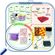

image file: d2ta02263j-p1.tif

Duoling Cao

Duoling Cao received her B.Sc. degree in Chemistry from Yangtze Normal University in 2020 and now is a master’s student of the School of Materials Science and Engineering, Hubei University, China. She is under the supervision of Associate Professor Dr Li Wan, doing research on designing the interface structure and carrier transport optimization of carbon counter electrode based perovskite solar cells.

image file: d2ta02263j-p2.tif

Wenbo Li

Wenbo Li received his B.Eng. degree in Polymer Materials Science and Engineering from Hubei University in 2020. He is currently a master’s student of the School of Materials Science and Engineering, Hubei University, China under the supervision of Associate Professor Dr Li Wan. His research focuses on performance optimization of all-inorganic perovskite solar cells.

image file: d2ta02263j-p3.tif

Xu Zhang

Dr Xu Zhang received her PhD degree in Physical Chemistry from the University of the Chinese Academy of Sciences in 2021. Now, she is working as a Lecturer at the School of Materials Science and Engineering, Hubei University, China. Her research focuses on perovskite materials, thin films, optoelectronics, etc.

image file: d2ta02263j-p4.tif

Li Wan

Dr Li Wan is an Associate Professor of new energy materials and devices at the School of Materials Science and Engineering, Hubei University, China. She obtained her PhD in Materials Science at Hubei University in 2011, working on low-cost carbon counter electrodes for dye sensitized solar cells. She worked as a Visiting Scholar at TU Wien, Austria from 2016 to 2017 and Shaanxi Normal University, China from 2018 to 2019. Her main research interests include high efficiency and low-cost photovoltaic devices like organic solar cells and perovskite solar cells, nano-carbon materials (carbon nanotubes and graphene), and composites for optoelectronic applications. Deep understanding of electrified interfaces is crucial to energy devices. Therefore, she has started to focus on researching in situ electrochemical characterization of electrified interfaces.

1. Introduction

Over the past few years, metal halide perovskites (MHPs) have succeeded as one of the new wonder materials not only for traditional areas of photovoltaics,1 light-emitting diodes (LEDs),2 photodetectors and photocatalysis,3,4 but also for many novel potential applications, such as X-ray imaging sensors,5,6 flexible scanners,7 photorechargeable ion batteries (IBs),8,9 biomedical detectors10–12 and information memory.13–15 Metal halide perovskites with bulk 3D form have a general chemical formula of ABX3, where A is an organic or inorganic monovalent cation (typically methylammonium, formamidinium or cesium), B is a divalent metal ion (Sn2+, Ge2+, or Pb2+), and X is a halide anion (Cl, Br, or I). Significantly, the most impressive development has so far been achieved undoubtedly in perovskite-light absorber based solar cells (PSCs) with the certified power conversion efficiency (PCE) reaching 25.5%,16 since being initially reported in 2009. The superior photovoltaic performances of PSCs have mainly been attributed to the excellent optoelectronic properties of MHPs, such as high optical absorption coefficients, long carrier diffusion length, low exciton binding energy and tunable bandgaps.17–20 However, lab-prepared single-junction PSCs are still far from the thermodynamic PCE limit and large-scale application despite their promising high PCE. One main reason for this has to do with the tremendous amounts of various types of imperfections/defects present in the perovskite layer and/or at relevant interfaces issuing from perovskite crystallization/composition and device/module fabrication processes due to the inherently ‘softer’ ionic crystal characteristics of MHPs.21–24 The existence of such defects in MHPs could result in ion migration, non-radiative recombination, hysteresis, charge trapping, charge scattering and even degradation of perovskites or metal electrodes, thereby negatively influencing the performance, stability, and scalability of PSCs.25 Recently, some effective defect-passivation strategies and agents like interface modification,26,27 and additive,28,29 solvent30,31 and composition engineering32,33 have successfully been developed for reducing defects in MHPs to improve the film quality and device properties by inhibiting non-radiative recombination, as well as prolong the carrier lifetime aiming for long-term stable and large-scale PSCs.34

Sharp tools make good work. Obviously, it is the results of characterization methods that can mainly help us to acquire deep mechanistic understanding of the fundamentals involved in the defect passivation of MHPs, which can then guide in choosing optimal defect passivation strategies to prepare MHP-based devices with high performance and long-term stability. So far, various techniques based on spectroscopy,35 microscopy, synchrotron and in situ neutron diffraction have been successfully employed for evaluating the chemical, morphological, structural, and optoelectronic properties of MHPs before and after the defect passivation. These tools have also been useful in elucidating the root causes of the Eloss, degradation mechanisms and low scalability of the PSCs. However, conventional methods based on X-ray, laser, or electron beam-based sources may accelerate the degradation of MHPs by a localized temperature increase, thereby producing severe artifacts during long-term characterization. Also, the current density–voltage (JV) and monochromatic incident photon-to-electron conversion efficiency (IPCE) characterization of full photovoltaic devices under light illumination may also give rise to hysteresis or phase separation due to ion migration and charge accumulation during measurement.35 Therefore, conventional characterization methods require optimization and suitable new in situ imaging techniques or operando measurement approaches also need to be developed for MHP and PSC research. Typically, capacitance measurements like drive-level capacitance profiling (DLCP),36 space-charge-limited-current (SCLC)37,38 and deep-level transient spectroscopy (DLTS),39 as well as spectrometric characterization methods like steady-state PL emission (ssPL)40,41 along with in situ techniques are new emerging characterization tools that might be used for an in-depth understanding of PSC materials (Fig. 1).


image file: d2ta02263j-f1.tif
Fig. 1 Summary of new characterization measurements applied to probing defect passivation in perovskite solar cell research. The inserted KPFM, STM, and in situ TEM images were reproduced with permission:141 copyright 2019, Elsevier.130 Copyright 2015, American Chemical Society.135 Copyright 2016, American Chemical Society.

Meng et al.35 reviewed some useful characterization methods used for MHPs and PSCs. Other published literature42,43 reviews/articles have briefly introduced commonly used techniques for the characterization of defects only mentioned in several paragraphs. However, timely reviews systematically focused on new measurements of defect passivation are still lacking. Moreover, a summary of in situ and operando characterization approaches for defect passivation is also needed. Therefore, specific reviews regarding this topic are imperative and urgently needed for providing useful guidance for further continuously boosting the development of PSCs. In the present review, we first give a short introduction to defects in MHPs, their influences on PSCs and progress in defect passivation. We then focus on summarizing and categorizing the current state-of-the-art advanced characterization techniques used for probing defect passivation so far, which are different from conventional characterization tools. Their limitations are also briefly discussed.

2. Characterization techniques for defect passivation

Different from ideal crystals, actually prepared MHPs have an incomplete crystal structure with various forms of defects. Point defects are the main form of defects in MHP crystals. Recently, many theoretical calculations have investigated the defect states of the most commonly used MAPbI3 perovskites with the crystal structure of ABX3 (Fig. 2a). Note that MAPbI3 native point defects include VMA, VPb and VI vacancies; interstitial MAi, Pbi and Ii; trans-substituted PbI, IPb, IMA and MAI; and cationic substituents PbMA and MAPb[thin space (1/6-em)]44 (Fig. 2b). It is generally considered that defects in perovskites with low formation energies have shallower energy levels near the valence band maximum or conduction band minimum, while defects with deep formation energies have higher formation energies in the band gap45 (Fig. 2c–e). Density functional theory (DFT) calculations confirmed that the energy levels of these defects in FAPbI3 are similar to those in MAPbI3, except that the antisites (FAI and IFA) create deep energy levels in FAPbI3 due to their lower formation energies.46 Li et al. found that in the α-phase of CsPbI3, under Pb-rich conditions, the energies of VPb and VI formation were the lowest among all acceptor and donor conditions, respectively.47 Huang et al. showed that most of the intrinsic defects in the δ-phase CsPbI3 induce deeper transition levels compared to γ-phase CsPbI3.48 More recently, Dunfield et al. linked the fault tolerance to the structural stability for perovskite materials.49 The structural tolerance coefficients of MAPbI3, CsPbBr3,50 CsSnI3,51 and MAPbBr3[thin space (1/6-em)]52 are about 0.82–0.85, whereas those of FAPbI3, CsPbI3, FASnI3, and MASnI3[thin space (1/6-em)]53 are outside this range. For polycrystalline perovskite films used in PSCs, other-dimensional (2D and 3D) defects like grain boundaries (GBs) may exist. Point defects would generate transition levels made mainly of Fermi level sites located near the conduction band minimum (CBM) or valence band maximum (VBM) representing shallow-level defect traps or within the forbidden band (deep-level defect traps) of MHPs. These transition levels may introduce charge recombination centers (traps) to trap free electrons or holes. Meanwhile, shallow-level defect traps with low charge recombination rates could affect the charge mobility to some extent. Deep-level defect traps, also known as Shockley–Read–Hall (SRH) recombination centers, may be annihilated with the anti-charge like non-radiative recombination process, thereby releasing part or all of the electrical energy in the form of phonons into adjacent lattices.45,54,55 This process can be detrimental to efficient charge extraction in PSCs. Impurity defects of extrinsic ions, such as Li+, Na+, and H+ issuing from the hole transport layer (HTL),56,57 deposited counter electrodes, and many other raw materials of PSCs, could migrate across the perovskite layer and strongly affect the charge separation at the charge transport layer (CTL)/perovskite interface and cause current–voltage hysteresis in PSCs. 2D defects, including GBs and surface defects, may reduce the bandgap and increase the coupling,58,59 thereby accelerating non-radiative charge recombination. 3D defects rely on the presence of metallic lead clusters in perovskite films generated by imbalanced I/Pb stoichiometry similar to the formation of halide vacancies. The concentration of metallic Pb has been demonstrated to be closely related to the density of states above the VBM and close to the Fermi level. Reduction of metallic Pb concentration may reduce such density of states and improve the photoluminescence quantum efficiency of perovskite films.60,61 In tin based PSCs, high concentrations of SnI2 and SnI4 will induce nonradiative recombination and shorten the carrier lifetime under the Sn-rich environments, while a high concentration of VSn electron acceptor defects can lead to a large number of background holes62 under tin-deficient conditions. The non-radiative recombination caused by defects may diminish the steady-state electron/hole density, charge lifetime, and charge diffusion length in PSCs, thereby resulting in severe degradation of PSC performance.
image file: d2ta02263j-f2.tif
Fig. 2 (a) Schematic representation of the ABX3 unit cell. (b) Illustration of a perfect lattice, vacancy, interstitial, anti-site substitution, Frenkel defect pair, Schottky defect pair, substitutional, and interstitial impurity group. (c–e) The calculated formation energies of intrinsic point defects in MAPbI3 at different chemical potentials. Reproduced with permission:45 copyright 2014, AIP Publishing LLC.

With the gradual rise of the PCE, the long-term stability of PSCs has been paid increasing attention. The main factors affecting the stability of PSCs include the crystal structure stability of MHPs, the interface and device structural stability, and degradation caused by environmental agents like water, oxygen, heat, light, and electricity.63–65 Essentially, all of these factors are closely related to the defects present in MHPs. For instance, exposure to humidity would cause water and oxygen molecules to penetrate into MHPs through the GBs in polycrystalline perovskite films, causing degradation of the perovskite layer.66,67 Under light exposure, the O2 present forms superoxide (O2), leading to deprotonation reactions accelerating the decomposition of MHPs.68 In the actual outdoor working environment (high temperature, water vapor, oxygen, etc.), the decomposition of perovskites is mainly reflected in the promotion of phase transition and perovskite ion migration, as well as the sensitivity to the external environment at high temperature. Additionally, the electric field may induce rapid migration of ions.69,70

The presence of defects in perovskite thin films not only directly affects the photovoltaic performance of PSCs through non-radiative recombination of photogenerated carriers but also reduces the long-term stability of MHPs and PSCs. Hence, various passivation strategies have so far been successfully applied to improve the efficiency and stability of PSCs. These methods include the introduction of additives, interface modification, component regulation, solvent engineering, single-crystal engineering,71–73 and electrochemical deposition.74–77 The passivation route relies on applying certain chemicals to react with surface components for deactivating their electronic or chemical activities. This approach generally reduces MHP defects and improves the device performance.42,43,78 Defect passivation could also change the contact resistance at the CTL/perovskite interface. The addition of passivation agents to perovskite precursors may improve the film morphology in terms of fewer pinholes, thereby increasing the filling factor of PSCs.

Combined with defect passivation strategies, many commonly used characterization techniques including microscopy, spectroscopy and electrical measurements have promoted PSC research. The clarifications provided by these tools about the structure, morphology, chemical composition, and optoelectronic and electrical properties of MHPs help further improve the quality of perovskite layers and the performance of PSCs. Since the performance and stability of PSCs are seriously affected by defects in perovskite layers, advanced characterization methods are required for a deep investigation of the defect characteristics of perovskite layers. Thus, several new characterization techniques for MHP trap states (density and energy levels) were reviewed in this article to gain a better understanding of the defect passivation mechanism in MHPs.

2.1 Capacitance measurements

Charged defects are equivalent to a localized capacitor, where trapped charges influence not only the electrical properties but also the capacitance characteristics of the semiconductor. Therefore, the features of a defect can be deduced by tracing the changes in capacitance under alternating current (AC) voltage.
2.1.1 Thermal admittance spectroscopy (TAS). Thermal admittance spectroscopy (TAS) is an established and effective technique broadly applied for measuring the defect density in solar cells (SCs). This includes both shallow- and deep-level defects measured by tracing the junction capacitance related to the defect density and its effectiveness as a dopant. TAS measurements at various temperatures are commonly used to reveal the defect density and energy distribution within the band gap in a semiconductor.79 In typical p–n junction SCs, the capacitance mainly originates from the charging/discharging of defects as a function of frequency change under AC voltage. Meanwhile, defect occupancy of the semiconductor is determined by the position of the Fermi level. As shown in Fig. 3a, electron traps below the Fermi level are assumed to be filled with photo-generated electrons. Upon changes in the frequency of AC voltage, the corresponding traps may release their charge within the AC period, thereby contributing to the admittance.80,81 The release of the charge depends not only on the energy depth of the defect but also on the temperature since the charge could thermally be activated and released to contribute to the admittance signal. Therefore, defect traps with different activation energies (Ea) at different modulated AC frequencies and temperatures are related to the junction capacitance.
image file: d2ta02263j-f3.tif
Fig. 3 (a) A schematic band diagram of a p-type semiconductor junction with a single trap level Ed and two measurement energies Eω1 and Eω2. Reproduced with permission:80 copyright 2015, Royal Society of Chemistry. Admittance spectra of (b) the reference PSC without TSP and the device with (c) CuI or (d) Cu(Tu)I as the TSP. Reproduced with permission:84 copyright 2017, American Chemical Society. Admittance spectra of WBG PSCs (e) without (the control) and (f) with the PEAI treatment. The derivative of admittance spectra of (g) the control device and (h) the device with the PEAI treatment. (i) Arrhenius plots of the characteristic transition frequencies derived from the admittance spectra. (j) Schematic of the energy barrier for ion movement in the control and the device with PEAI treatment. Reproduced with permission:85 copyright 2020, American Chemical Society. (k) tDOS for devices without PCBM (orange), with PCBM but no thermal annealing (red), with 15 min thermal annealing of PCBM (green), and 45 min thermal annealing of PCBM (blue). Reproduced with permission:82 copyright 2014, Springer Nature. (l) Trap density of states obtained by thermal admittance spectroscopy for devices with PCBM (blue), and choline chloride passivation layers (red). Reproduced with permission:86 copyright 2017, Springer Nature. (m) TAS plots of the PSC devices. Reproduced with permission:87 copyright 2019, Elsevier. (n) Trap density of states (tDOS) for devices without CsBr (black) and with CsBr modification (red). Reproduced with permission:88 copyright 2013, Royal Society of Chemistry. (o) tDOS characterization for the PSCs based on control MAPbI3 and g-C3N4 modified MAPbI3 films. Reproduced with permission:89 copyright 2012, Royal Society of Chemistry. (p) Those of the WBG MAPbIxBr3−x perovskite solar cells based on ICBA-mixture and ICBA-tran3. Reproduced with permission:90 copyright 2017, Wiley-VCH.

The energy of the defect energy level Ea at frequency ω and the characteristic attempt-to-escape frequency ω0 can be expressed according to eqn (1) and (2):82

 
Ea = EdEν(1)
 
image file: d2ta02263j-t1.tif(2)
where Eν, Ed, ω0, and β are the VBM energy level, energy depth of the defect, attempt-to-escape frequency, and a temperature-dependent parameter, respectively.

Below Ea, defect traps could capture or emit charges and contribute to the capacitance. The defect density may derive from the angular frequency-dependent capacitance using eqn (3):82

 
image file: d2ta02263j-t2.tif(3)
where C and ω represent the capacitance and angular frequency, respectively. Vbi and W are the built-in potential and depletion width of the target material extracted from capacitance–voltage measurements and Mott–Schottky analysis, respectively.

Typical analyses of capacitance–voltage scans for Schottky junctions are often based on depletion approximation by assuming no free charges at the junction in the space charge region. In this case, the charge in this region entirely originates from dopant atoms or molecules, and depletion width W can be expressed as:83

 
image file: d2ta02263j-t3.tif(4)
where εr and A are the relative dielectric constant and contact area, respectively.

Ye et al. compared the defect passivation effect of CuI and Cu(Tu)I in MAPbI3−xClx by the TAS method.84 The calculations of temperature-dependent admittance spectra of devices without and with trap state passivation (TSP) at various temperatures (T = 230 K to 300 K) from 10 to 105 Hz in the dark demonstrated that Cu(Tu)I had a better defect passivation effect than CuI (Fig. 3b–d). Arrhenius plots of characteristic transition frequencies correspond to admittance derivatives and the calculated Ea of pure perovskites and perovskites–Cu(Tu)I are 0.318 and 0.388 eV, respectively. The higher Ea value in the latter indicates that the ion migration in the perovskite layer is significantly suppressed after treatment with Cu(Tu)I. Chen et al. used TAS measurements on wide-bandgap (WBG) FA0.8Cs0.2Pb(I0.7Br0.3)3 perovskite-based PSCs without and with the phenethylammonium iodide (PEAI) treatment to elucidate the suppression of ion migration.85 Their data showed that suppression of mobile ionic defects might reduce the formation of charge defects acting as non-radiative recombination centers. Their recent work revealed the usefulness of low-frequency capacitance measured by the TAS technique for estimating the activation energy (EA) of ion motion in perovskite absorber layers. The TAS spectra of PSCs without and with PEAI treatment were measured from 250 to 300 K in the dark (Fig. 3e and f) and the derivative of the capacitance–frequency spectra was used to obtain the characteristic transition frequency values (ωpeak) (Fig. 3g and h). The Ea values were calculated by fitting the corresponding Arrhenius plots using the formula ωpeak = βT2[thin space (1/6-em)]exp(−Ea/kT), where β refers to a temperature-related prefactor. Their findings indicated an Ea of 0.905 eV obtained by the device subjected to PEAI treatment. This value was higher than that of the control device (0.680 eV) (Fig. 3i and j). The higher Ea value indicates that the ion migration in the perovskite layer is significantly suppressed after treatment with PEAI. Suppression of mobile ion defects is also expected to reduce the formation of charge defects, which can act as nonradiative recombination centers. The substantially higher Ea indicated significantly suppressed ion migration in the perovskite layer after PEAI treatment. Shao et al. used a typical curve of trap density of states (tDOS) versus defect energy level Ea to investigate defect passivation by PCBM in MAPbI3 based PSCs.82 They found that Ea below 0.4 eV (band 1, 0.35–0.40 eV) could be assigned to a relatively shallow-level defect trap, while Ea above 0.4 eV (band 2 and band 3) may be indexed to deeper levels (Fig. 3k). The PSCs containing a PCBM layer without thermal annealing illustrated significantly reduced tDOS at band 2 and band 3. By comparison, PSCs containing a PCBM layer and subjected to annealing revealed efficiently more reduced shallow-level defect traps. Therefore, the deep-level defect trap located at the MAPbI3 film surface was effectively passivated by PCBM without thermal annealing. The even deeper shallow-level defect traps found in MAPbI3 films can only be passivated by diffusion of PCBM into the MAPbI3 inner layer. Zheng et al. utilized the TAS method to clarify the better passivation effect of choline chloride when compared to PCBM by considering both cationic and anionic defects in MHPs during passivation strategies.86 The obtained device with choline chloride layers showed the lowest tDOS over the whole trap depth region (Fig. 3l), while the low tDOS in the deeper trap region of 0.40–0.52 eV was assigned to defects at the film surface. Furthermore, the density of shallower trap states in the choline-chloride-passivated devices (0.35–0.40 eV) assigned to traps at GBs was about 3-fold smaller than that in PCBM-passivated devices, indicating the diffusion of choline chloride and passivation of the GBs.

Overall, defects are very important and are thus further investigated since defects in the MAPbI3 perovskite layer change significantly. For instance, Zhang et al. studied the tDOS through TAS measurements. The tDOS values for a TB(MA) modified PSC with a backbone composed of a 2,5-dialkoxy-1,4-phenylene unit and thiophene unit, and side-chain end-capped by –SO3– MA+ were found to be more than one order of magnitude lower in the entire energy range.87 The exact densities of shallow- and deep-level defect traps were calculated to be 9.59 × 1015 cm−3 and 1.94 × 1017 cm−3 for the TB(MA) modified device, respectively. By comparison, 2.43 × 1017 cm−3 and 5.09 × 1018 cm−3 were recorded for the control device (Fig. 3m), respectively. Thus, fewer interface defects were obtained by the TB(MA) passivator. Li et al. further examined the energetic profile of tDOS at the MAPbI3−xClx perovskite/TiO2 interface by performing TAS on complete photovoltaic devices. Their data revealed a decline in tDOS from 5.0 × 1016 cm−3 (without CsBr) to 2.0 × 1016 cm−3 (with CsBr) (Fig. 3n), confirming enhanced electronic contact between perovskites and c-TiO2 through CsBr modification and resulting in improved interface stability.88 Liao et al. measured TAS for quantifying the tDOS of devices fabricated with and without the g-C3N4 additive (Fig. 3o). The g-C3N4 modified device illustrated remarkably reduced tDOS in the deeper trap region (0.40–0.55 eV) corresponding to defects at the film surface, as well as a shallower trap region (0.30–0.40 eV) assigned to traps at GBs.89 This confirmed that doping of g-C3N4 might enlarge the grain size and improve the crystallinity, thereby passivating the defects. Moreover, the soft and mechanically flexible framework of g-C3N4 could passivate poorly coordinated ions at the GBs or on MAPbI3 film surfaces. Lin et al. measured the TAS of tDOS in devices composed of two different electron transfer layers (ETLs) to figure out the origin of the charge-carrier lifetime enhancement by replacing the indene-C60 bisadduct (ICBA)-mixture with ICBA-tran3.90 To this end, a simple method was applied to reduce the energy disorder by isolating the isomer ICBA-tran3 from the as-synthesized ICBA-mixture. The obtained density of defect states ranged from 1 × 10¹⁶ to 1 × 10¹⁹ m−3 for both types of PSCs. The tDOS was almost identical for the ICBA-tran3 and ICBA-mixture based WBG MAPbIxBr3−x PSCs with values estimated to be 0.42–0.55 eV (Fig. 3p). The tDOS values of the shallower traps (0.35–0.42 eV) in ICBA-mixture based devices were larger than those of ICBA-tran3 devices, revealing a slightly weaker passivation effect by the ICBA-mixture.

2.1.2 Drive-level capacitance profiling (DLCP). TAS has widely been used for analysis of tDOS but is unsuitable for profiling the spatial distribution of tDOS in semiconductor films or crystals. Alternatively, Ni et al. demonstrated the usefulness of the drive-level capacitance profiling (DLCP) method for characterizing the spatial and energetic distributions of carrier and trap densities in PSCs.36 In Fig. 4a, X denotes the distance from the junction barrier (n+–p junction) where the traps may be able to dynamically change their charge states as a function of AC bias δV, and δX refers to the differential change in X with respect to δV. The DLCP method exploits the dependence of junction capacitance on the magnitude of AC voltage (δV) to yield the trap density at X position.91,92 The DLCP technique also allows deriving the energetic distribution (Eω) of trap states by tuning the frequency of AC bias or temperature (T), similar to TAS measurements. In this way, both the trap density and trap depth could be extracted. The trap states at different positions in real space might also be obtained by changing the DC bias applied to the depletion region of the junction. The specific procedures for analyzing tDOS with the DLCP method can be found in related literature.
image file: d2ta02263j-f4.tif
Fig. 4 (a) Schematic of band bending of a p-type semiconductor with deep trap states in an n+–p junction. (b) Dependence of the trap density on the profiling distance of a MAPbI3 single crystal measured by DLCP. (c) Spatial distributions of trap states in a MAPbI3 thin single crystal, as measured by DLCP. Reproduced with permission:36 copyright 2020, American Association for the Advancement of Science. (d) Characteristic IV trace (purple markers) showing three different regimes for MAPbBr3 (at 300 K). Reproduced with permission:38 copyright 2015, American Association for the Advancement of Science. (e) Dark current–voltage curves of electron-only devices with the FTO/TiO2/perovskite (BAI)/PCBM/Ag structure. Reproduced with permission:96 copyright 2020, Wiley-VCH. (f) Dark current–voltage curves of the CsPbIBr2 PSC devices with the FTO/TiO2/perovskite/PCBM/Ag structure. Reproduced with permission:97 copyright 2019, Wiley-VCH. Dark current–voltage curves from (g) electron-only and (h) hole-only devices based on 0.0% and 1.0% Pb(SCN)2 with the structure shown in the inset. Reproduced with permission:98 copyright 2019, Wiley-VCH. Current density–voltage characteristics of (i) hole- and (j) electron-only devices for estimating defect density in the 2D perovskite film. Reproduced with permission:99 copyright 2020, American Chemical Society. (k) Thermally stimulated current for the devices with a CuSCN HTL (green), a PEDOT:PSS HTL (red), and without transport layers (purple). The dark TSC reference measurement for the ITO/CuSCN/MAPI/PCBM/C60/Au configuration is also shown (black). (l) Arrhenius plots of the initial rise of the T4 TSC peak for the devices with a CuSCN HTL (green), a PEDOT:PSS HTL (red), and without transport layers (purple). Reproduced with permission:102 copyright 2015, American Chemical Society.

Ni et al. obtained profiling of spatial and energetic distributions of trap states in metal halide perovskite single-crystalline and polycrystalline solar cells.36 Their results suggested trap densities in single crystals varying by five orders of magnitude, with the lowest value estimated to be 2 × 10¹¹ per cubic centimeter, and most deep traps were located at crystal surfaces. Also, symmetric distribution of the trap density was observed (Fig. 4b), consistent with the structural symmetry of the double-side polished MAPbI3 single crystal. The spatial profiling of trap densities in MAPbI3 single crystals was also performed by DLCP and the data illustrated about 10-fold greater trap density near the interface region than inside the MAPbI3 single crystal. Thus, dangling bonds at the surface of the crystal formed charge traps. To gain a better understanding of the relationship of trap density and distribution, DLCP measurements were also conducted on devices with the ITO/PTAA/MAPbI3 (39 μm)/C60/BCP/Cu structure based on a typical MAPbI3 thin single crystal synthesized by a space-confined growth method (Fig. 4c). The increase in carrier density with the decrease in AC frequency confirmed the existence of charge traps contributing to junction capacitance at low AC frequencies (large Eω) in the MAPbI3 thin single crystal. The trap density distribution in the MAPbI3 thin single crystal synthesized by the space-confined method was different from that in the bulk crystal. The trap density in the MAPbI3 thin single-crystal varied by up to 5-fold, and the trap density near both surfaces was 2- to 4-fold higher than that in bulk crystals. Furthermore, trap density decreased gradually toward the center of the crystal, and its distribution along the normal direction was not symmetric despite the contact between both surfaces of the thin single crystal with PTAA/ITO during growth.

2.1.3 Space-charge-limited-current (SCLC). The defects present in semiconductors could capture and trap free charges, thereby altering the electrical properties of materials after filling of the defects. Space-charge limited current (SCLC) has widely been utilized to measure properties associated with defects, including conductivity, carrier concentration, carrier mobility, and defect density.37 In the SCLC method, the subjection of a semiconductor to a sufficiently large electric field through ohmic contacts would inject electric charges into the material to generate a current flow. The defect sites present will capture some of the injected charges, thereby reducing the density of free charges. Since the current is limited by the space-charge effect, the defect density in the semiconductor can be obtained from the curve of current vs. voltage (IV) in the region of space-charge-injected current.93

The IV curves are often plotted on a double logarithmic scale and analyzed according to SCLC theory. Fig. 4d shows a typical IV curve of PSCs based on MAPbBr3 single crystals divided into three regions:38 the ohmic region, the trap-filled limit (TFL) region, and the Child region. At low voltages, the IV curve (labeled in blue) can be linearly fitted to IVn=1 when defects are filled by some injected charges. After filling all defects by charges at a particular onset voltage, the injected charges will freely move through MAPbBr3, leading to a rapid jump in current reaching the low resistance state at the onset voltage of the trap-filled limit (VTFL). As a result, the defect (trap) density (ntrap) can be estimated according to eqn (5):38

 
image file: d2ta02263j-t4.tif(5)
where L, εr, εo, and e are the thickness of the MHP film, dielectric constant of the material, permittivity of vacuum, and electronic charge, respectively.

For MHPs, the defects can either be hole-traps or electron-traps.

Recently, the SCLC method has not only been used to analyze the trap-state density and carrier mobility of MHP single crystals,94,95 but also for defect passivation of PSCs. A better understanding of associated optoelectronic properties requires accurate characterization of trap density in MHPs. Hence, SCLC was employed in our work to explore the decrease in trap state density and restrained non-radiative recombination in all-inorganic CsPbIBr2 PSCs by incorporating butylammonium iodide (BAI) (Fig. 4e). The trap densities of pristine and modified CsPbIBr2 perovskite films were calculated to be 6.8 × 10¹⁵ and 3.4 × 1015 cm−3, respectively.96 Thus, BAI modification could reduce the trap state density to achieve superior crystallinity and morphology, conducive to better device performance. We also analyzed the trap-state density of pristine CsPbIBr2 film and 0.7% sulfamic acid sodium salt (SAS)-incorporating CsPbIBr2 film.97 The calculated Nt of the CsPbIBr2 film with and without SAS are 5.10 × 10¹⁵ and 6.24 × 1015 cm−3, respectively (Fig. 4f). In region n = 2, the carrier mobilities of CsPbIBr2 with and without additive were calculated to be 3.03 × 10⁻³ and 2.75 × 10⁻³ cm2 V−1 s−1, respectively. Therefore, effective defect passivation occurred in the bulk CsPbIBr2 film by SAS. Ye et al. reported a CsPbI2Br film with 1.0% Pb(SCN)2 with higher current density than that of the pristine film, indicating a smaller resistance and better charge transport properties.98 Ye et al. also used SCLC (Fig. 4g and h) to investigate the influence of Pb(SCN)2 on the trap states of CsPbI2Br films and final PSCs. Their data revealed a linear interrelationship between current and bias voltages at low bias voltages, while the current increased nonlinearly with voltage at higher bias voltages. Both the electron-only and hole-only devices with 1.0% Pb(SCN)2 exhibited lower VTFL values, implying significantly reduced electron trap densities by Pb(SCN)2.

The SCLC method has also been applied to investigate different defect behaviors in 2D perovskites in comparison with 3D perovskites. In this respect, Liu et al. utilized SCLC measurements to gain a better understanding of the charge trap density and carrier mobility in 2D BA2MA3Pb4I13 perovskite films.99 The current density–voltage (JV) curves of electron-only and hole-only devices were used to calculate the hole and electron trap density in 2D perovskite films (Fig. 4i and j). Values of 8.22 × 10¹⁶ and 6.82 × 1016 cm−3 were obtained, which were significantly higher than those of previously reported 3D perovskite films (4.12 × 1015 cm−3 and 3.22 × 1015 cm−3), respectively. Consequently, more severe carrier recombination may have occurred in 2D perovskite films. Besides, the fitted JV curves at the SCLC region induced hole and electron mobility of approximately 5.31 × 10⁻² and 5.64 × 10⁻² cm2 V−1 s−1, respectively, for 2D perovskite films. These values were considerably lower than those of 3D perovskite films, indicating decreased carrier mobility and impediment of carrier transmission by introduction of long-chain butylamine as a spacer.

2.1.4 Thermally stimulated current (TSC). Thermally stimulated current (TSC) is a technology based on dielectric physics widely used to study trap energy level distribution and surface transport of carriers in MHPs.100 To conduct TSC measurements, the device should first be cooled to a very low temperature, and carriers were then generated by illumination. Afterward, the device was kept at a constant temperature to allow carriers to relax the internal density state and occupy possible trap states. After the thermalization process, the temperature was raised slowly at a constant rate to release trapped electrons. The shallow-level trap was released at low temperatures, while the deep state carrier current was released at higher heat energy. The generated ITSC was then detected to construct TSC curves. The trap density nt on the material surface can be determined by relevant processing of TSC curves and calculations using eqn (6) and (7).101
 
image file: d2ta02263j-t5.tif(6)
 
image file: d2ta02263j-t6.tif(7)
where EA represents the activation energy, kB is the Boltzmann constant, T refers to the temperature, e is the basic charge, and V denotes the sample volume.

Baumann et al. used TSC measurements to study the electron trap states of MAPbI3 planar PSCs composed of ITO/poly(3,4-ethylenedioxythiophene):poly(styrenesulfonate) (PEDOT:PSS)/MAPbI3/PCBM/C60/2,9-dimethyl-4,7-diphenyl-1,10-phenanthroline (BCP)/Au (red curve, Fig. 4k) and ITO/CuSCN/MAPbI3/PCBM/C60/BCP/Au (green curve, Fig. 4k).102 For each device, the TSC trajectory was plotted as a function of temperature. The two peaks at very low temperatures (T1 and T2) were low-level defect traps in the PCBM/C60 electron transport layer owing to the absence of the electron transport layer. Also, the two low-temperature peaks vanished, indicating that most shallow traps must be located in the transport layer instead of the perovskite layer. The other two TSC peaks at higher temperatures were assigned to the perovskite layer. The first peak was attributed to the phase transition of the perovskite crystal around T3 (163 K), and the second peak at around T4 (194 K) was related to the charge trap analyzed using the initial ascent method. The activation energy of the trap state in MAPbI3 perovskite films at T4 was calculated according to eqn (6) and Arrhenius plots and the resulting value was about 508 ± 20 meV (Fig. 4l). The lower limit of defect density was calculated using eqn (7) to be 1 × 10²¹ m−3.

2.1.5 Deep-level transient spectroscopy (DLTS). The release of charges captured by shallow-level defects could influence the electrical properties of semiconductors. Deep-level transient spectroscopy (DLTS) analysis has improved features related to sensitivity, range of observable defect depths, and facile operation.103 Using DLTS, the emission rate window may easily be set and the instrument would only respond when a transient is detected with a rate within the set window. Thus, the variation of the emission rate of a defect in the set window at different temperatures would yield a response peak at each specific temperature. The main principle of DLTS consists of using the variation in defect emission rate versus temperature to determine the energy differences between defect states and one band edge, as well as capture the cross-section of the defects.104

In typical DLTS, the capacitance transients are investigated by measuring the variations in capacitance as a function of temperature, usually in the range from liquid nitrogen temperature to room temperature (300 K) or above. During the initial bias pulse at low temperatures, defects could be filled by bias-generated charges. During this process, the capture rate of a defect trap should be much larger than its emission rate, making the latter negligible. The increase in temperature will yield DLTS peaks if the emission rate of a charge trapped by defects is within the set rate window. Hence, the defect density can directly be obtained from the capacitance change corresponding to the complete filling of the defect traps with a saturated injection pulse or the largest possible majority-carrier pulse. The defect density at a certain temperature can be described by eqn (8):103

 
ntrap = 2(ΔC/C)(NAND)(8)
where ΔC and C are the capacitance change from t = 0 and the capacitance of the diode under quiescent reverse-biased conditions, respectively. NAND represents the net acceptor concentration on the p side of the junction.

The EA of the defects below the conduction band can be obtained according to eqn (9):103

 
image file: d2ta02263j-t7.tif(9)
where en, σn, vn, ND, and gn are the thermal emission rate of trapped charges, charge capture cross-section, mean thermal velocity of charges, effective density of states in the carrier band, and degeneracy of defects, respectively.

To distinguish the nature of defects (electronic or ionic) in MAPbI3 perovskites, Reichert et al. applied reversed DLTS, meaning voltage change from 1 V to 0 V.39 Other parameters, such as AC frequency and filling-pulse, remained constant. Unlike conventional DLTS measurements, the capture charge carriers' process in trap states was measured because of electronic traps. Since the emission rate was much lower than the capture rate, the latter (determined by reverse DLTS) was higher than the emission rate (obtained by conventional DLTS) when deep-level trap states were measured. The situation was different when mobile ions responded to voltage pulses. In the absence of applied external voltage, mobile ions were in an equilibrium state at the interfaces of perovskite layers due to the internal field. As a result, mobile ions were pushed into the perovskite layer by a voltage pulse. For ions, this process would be approximately as fast as the back drift of ions to the interfaces. The measured reverse DLTS at room temperature and the plot of boxcar evaluation at a rate window of t2/t1 = 2 are provided in Fig. 5a. The emission rates of all defects looked comparable for the conventional and reverse DLTS. Hence, the measured emission rates originated from mobile ions instead of charge carriers, such as electrons and holes. After conducting DLTS tests of PSCs following algorithm analyses, three different types of mobile ions corresponding to different examples of defect parameters were recorded. Notably, the strong capacitance freeze-out presented a serious obstacle for DLTS measurements. Here, the dominant feature consisted of a very prominent peak near 150–200 K related to the rapid increase in capacitance as a function of temperature. This produced a false peak, not associated with a deep level trap as clearly shown by the independence of the peak position of the time window. However, the signal of real traps became considerably distorted by the false peak arising from capacitance freeze-out. To eliminate this effect and obtain clean spectra, Polyakov et al. corrected the signal by a known rate of change with temperature of the steady-state capacitance in DLTS of MAPbI3 perovskites.105 The corrected DLTS signal (Fig. 5b) showed two features at high temperatures (>200 K). The first was related to a hole trap (negative peak A according to convention in Fig. 5b, that is the capacitance decreases with time during the transient) while the other was linked to electron traps (positive peak B). Unlike false peaks, such peak positions moved as a function of the time window, thereby belonging to real traps. The slight temperature dependence of the electron trap peak B intensity resulted from interference with the hole trap peak A, while the stronger temperature dependence of the hole trap peak A intensity issued from the temperature dependence of free electron concentration. The hole trap displayed an activation energy of 0.57 eV and a capture cross-section of 4.2 × 1017 cm2, whereas the corresponding values of the electron trap were around 0.74 eV and 2.7 × 1016 cm2, respectively. The energies of such trap levels agreed reasonably with state-of-the-art density functional calculations that predicted the existence of interstitial iodine defects at energies of 0.57 eV and 0.8–0.9 eV of the conduction band for the first two levels.


image file: d2ta02263j-f5.tif
Fig. 5 (a) Conventional DLTS and reverse DLTS evaluation via boxcar at room temperature with a rate window of t2/t1 = 2. Reproduced with permission:39 copyright 2020, American Physical Society. (b) DLTS spectra as corrected for the strong capacitance freeze-out, and various time windows t1 and t2. Reproduced with permission:105 copyright 2018, AIP Publishing. (c) FWHM of the emission peak and average transient PL lifetime (τPL) as a function of the pump fluence. τPL is the time taken for the intensity to decrease to 1/e of its initial value. (d) PL intensity as a function of pump fluence. The dashed vertical black lines in (c) and (d) indicate the onset of ASE. Reproduced with permission:107 copyright 2014, Nature Publishing Group. (e) Face emission spectra of FAPbI3 film pumped by a pulsed laser with a duration of 150 fs. (f) Face emission spectra of MAPbI3 film pumped by a fs pulsed laser. The insets show the integrated emission intensity and the FWHM of the face emission spectra as a function of pump energy. Reproduced with permission:40 copyright 2017, American Chemical Society.

2.2 Spectrometric characterization

Carrier dynamics is the key issue when studying the performance of semiconductor devices. Efficient carrier transport refers to the transfer of electrons and holes from one monomer to another without being dispersed or captured by traps. Carrier mobility can indirectly provide useful defect information. In this section, we briefly review the methods for measuring carrier mobility in PSCs, including steady-state PL emission (ssPL), transient absorption (TA) spectroscopy, photo-induced charge extraction with linearly increasing voltage (photo-CELIV), time-resolved microwave conduction (TRMC) method and time-resolved Kerr rotation (TRKR) measurement.
2.2.1 Steady-state PL emission (ssPL). In steady-state PL emission (ssPL) measurements under ambient conditions, MHP films become photo-excited with the increase in pump fluence, thereby exhibiting correlated photoemission properties. After photo-excitation, the excited-state carriers in MHP films are emitted through band gap relaxation or trapped by defect traps. The turning point of low pump fluence represents photo-generated charge required to fill all defect traps, meaning the threshold trap pump fluence Ptrapth. The total defect density ntrap (bulk and surface) can be estimated following eqn (10):106
 
image file: d2ta02263j-t8.tif(10)
where α and E represent the absorption coefficient and energy of a photon at the laser pulse wavelength, respectively.

At low pump fluence, the Auger recombination is negligible, and defect-mediated charge recombination should be much slower than the band-edge radiative recombination. The bulk/surface corresponding defect density of states can be calculated using relevant kinetic equations.

Xing et al. used ssPL to reveal the existence of two types of traps in MAPbI3 films (Fig. 5c and d).107 The bulk density of defect states was estimated to be 5 × 1016 cm−3, while the density of defect states on the surface was about 1.6 × 1017 cm−3. Yuan et al. employed ssPL spectroscopy to compare the defect state densities of MAPbI3 and FAPbI3 films as a function of pump fluence.40 As shown in the inset of Fig. 5e, the first intersection representing the pump energy required filling all the traps, meaning the threshold trap pump energy (about 1 μJ cm−2) corresponding to a trap state density of about 1017 cm−3. In contrast, the MAPbI3 film had a higher threshold (about 6 μJ cm−2) than the FAPbI3 film, indicating an elevated density of trap states (about 2.5 × 1017 cm−3) (Fig. 5f).

2.2.2 Transient absorption (TA) spectroscopy. Transient absorption (TA) spectroscopy, also known as pump–probe technology, was first applied in the field of photochemistry. Nowadays, TA measurements are used to study the energy transfer and charge transfer processes in semiconductors after light absorption.76,108 Hence, TA might be employed for further design of PSCs and improve the performance of devices. In TA, small amounts of samples are excited by high-energy pump light to release energy instantaneously and excite the sample from the ground state to the excited state. Next, the same point of the sample is irradiated with another weak broadband white light (probe light). The intensities of the probe light and reference light after passing through the sample can be measured with a high precision detector (CMOS/NMOS) by adjusting the time delay between the pump light and probe light with an optical delay line. The differential absorption spectrum of the sample can be obtained by recording the detection light and reference light intensities of the sample with and without pump light by controlling the passage and occlusion of the pump light with a chopper. In general, the change in absorption ΔA of a sample can be calculated using eqn (11):
 
ΔA(λ) = −log{[I(λ)pro/I(λ)ref]pump/[I(λ)pro/I(λ)ref]unpump}(11)
where ΔA(λ) represents the change in absorption as a function of detection wavelength, I is the light intensity measured by the detector, [I(λ)pro/I(λ)ref]pump refers to the ratio of light intensities of the probe light and reference light when the pump light passes through the sample, and [I(λ)pro/I(λ)ref]unpump denotes the ratio of the intensity of the probe light to the reference light when the pump light is blocked.

The carrier relaxation process of a sample can be analyzed using a linear stage to adjust the time delay of the probe light reaching the sample surface relative to the pump light, as well as record changes in probe light absorption spectroscopy under continuous-time delay. However, unlike steady-state absorption spectroscopy, the ΔA(λ) of the transient absorption spectrum contains positive (+) and negative (−) signals, where the signal may change from positive to negative or vice versa. For example, the signals of molecular systems usually originate from contributing excited state absorption (ESA) signals, ground state bleaching (GSB) signals and stimulated emission (SE) signals. Liu et al. used the TA measurement method to reveal the excellent carrier dynamics of a perovskite layer with complete defect passivation.75 A sharp photo-bleaching (PB) signal band carrier decay was observed in the band edge of CsFAMA perovskites in accordance with the dominant band-to-band carrier recombination (Fig. 6a–c). Two negative ΔA valleys were detected at approximately 480 nm (PB1) and 760 nm (PB2), caused by the combination of PB and SE signals (Fig. 6d–f). Note that the generation, decay, and recombination of carriers in perovskites mainly depend on the PB signal in the band-edge region. In the initial stage from 0 to 5 ps, the changes in PB2 peaks of perovskite samples were independent of the introduced cysteamine hydrochloride (CAS-Cl) since 3D perovskites generally possess Wannier–Mott type excitons due to the low exciton binding energy (≈12 meV). The PB2 peak of pristine perovskites started to vanish at 994.6 ps after excitation to become almost quenched at 2013.6 ps. By comparison, the PB2 peak of double-defect passivation or full-defect passivation perovskites stabilized for a longer time, confirming the longer lifetime of defect-passivated perovskite films (Fig. 6g). Meanwhile, the carrier lifetime of perovskite films increased after double passivation or full passivation (Fig. 6h).


image file: d2ta02263j-f6.tif
Fig. 6 The pseudocolor TA plots for (a) the control perovskite film and the perovskite films with (b) dual defect passivation and (c) full defect passivation. TA spectra showing the PB1, PB2, and PA signatures at various probe delays for perovskite films (d) without CAS-Cl passivation, (e) with dual defect passivation, and (f) with full defect passivation. (g) 400 nm pumped TA kinetics probed at the PB2 peak and (h) biexponential function fitted TrPL spectra for the perovskite films. Reproduced with permission:75 copyright 2020, Wiley-VCH GmbH.

Li et al. used femtosecond TA measurements to confirm the enhanced phase purity and suppressed nonradiative recombination in quasi-2D perovskite films.109Fig. 7a and d show two signals: negative (blue) GSB and positive (yellow) ESA. For the pristine quasi-2D CsPbI3 film, the positive band at ≈500 nm in the short wavelength region belongs to the low-dimensional phase ESA, while it is not obvious in the optimized film, indicating that the N-methyl-2-pyrrolidone iodide (NMPI) additive can improve the phase purity. TA spectra at different time scales of charge carrier dynamics are shown in Fig. 7b and e. After 5 ns, the bleaching signal of the pristine quasi-2D CsPbI3 film decays almost completely, while the optimal bleaching signal shows a clear signal, indicating a longer decay time for carriers after the introduction of NMPI additive. Furthermore, the TA kinetics of the pristine and optimized quasi-2D (n = 20) CsPbI3 films (Fig. 7c and f) show that the carrier extraction time of the pristine quasi-2D CsPbI3 film (725 fs to 26.8 ps) is shorter than that of the optimized film (2–204 ps), but the τ3 of the latter is 10 times longer than that of the pristine film (3180 vs. 289 ps). The prolonged τ3 suggests that the NMPI additive optimized the crystallization kinetics of quasi-2D CsPbI3, improved the morphology and phase purity, and thereby enhanced the carrier lifetime and reduced the trap density.


image file: d2ta02263j-f7.tif
Fig. 7 TA spectra obtained following a 400 nm laser pulse excitation of the (a–c) pristine (0% NMPI) and (d–f) optimized (2% NMPI) quasi-2D (n = 20) CsPbI3 films: (a and d) Time- and wavelength-dependent 3D plot TA images; (b and e) TA spectra at selected probe times; (c and f) the TA kinetics curves. Reproduced with permission:109 copyright 2021, Wiley-VCH GmbH. (g) Implementation of the insulating layer into the solar cell structure for charge selective photo-CELIV. (h) Correlation between charge carrier mobility and photogenerated light intensity governed by the applied laser pulse, for control and charge selective samples after a 7 μs pulse delay. Reproduced with permission:114 copyright 2017, Wiley-VCH Verlag GmbH & Co. KGaA, Weinheim.
2.2.3 Photo-induced charge extraction by linearly increasing voltage (photo-CELIV). The photo-CELIV technique characterizes defects by testing the carrier mobility to confirm the passivation effect. Following the pioneering work of Juska et al., photo-CELIV has been widely used to study charge transport in organic semiconductor films.110,111 In photo-CELIV measurements, charge carriers are photogenerated in semiconductor layers. Subsequently, photo-induced carriers are extracted by applying a linear voltage pulse (reverse bias), and the corresponding transient extraction current can be obtained from eqn (12):112
 
j(t) = j0 + Δj(t)(12)
In eqn (12), Δj is the average conduction current of mobile charge carriers within the active layer. j0 = CA is the average displacement current, where C is the geometric capacitance of the active layer and A is the voltage rise rate. Feature extraction time tmax is observed when a linearly increasing voltage is applied to a sample with blocked contacts. Under the condition of Δjj0, the mobility μ is given by eqn (13):113
 
image file: d2ta02263j-t9.tif(13)
where d is the sample thickness, A is the applied voltage gradient and tmax is the maximum carrier extraction time. By integrating the CELIV transients, the equilibrium and photogenerated carrier densities can be obtained in the dark and in the light, respectively. By varying the delay time between excitation and voltage sweep, excited carrier dynamics on the microsecond timescale can also be obtained, which can reveal relevant information about carrier recombination within the device.

Petrović et al. explored the charge carrier mobility and transport properties of mesoporous and inverted planar-structured PSCs by the photo-CELIV technique (Fig. 7g).114 It was found that highly balanced charge mobilities were obtained in mesoporous devices, whereas in planar devices, the hole mobility was a half order of magnitude lower than the electron mobility due to the inferior hole injection ability from poly(3,4-ethyledioxthiophene) polystyrene sulfonate (PEDOT:PSS) to the spiro-OMeTAD interlayer (Fig. 7h). Furthermore, dispersive transport is found in electron-selective devices with TiO2 ETLs, which indicates the presence of a considerable number of trapped states at the perovskite interface, whereas the planar devices do not have these trapped states. Chen et al. determined the hole and electron mobilities of CH3NH3PbI3 perovskites by the photo-CELIV technique and revealed the recombination process and trap states. The results show that efficient and balanced transport is achieved in both CH3NH3PbI3 pure films and CH3NH3PbI3/phenyl-C61-butyric acid methyl ester (PC61BM) bilayer solar cells.115 Furthermore, the charge mobility of the pure CH3NH3PbI3 film was 3.2 × 10⁻⁴ cm2 V−1 s−1, which is almost doubled to 7.1 × 10⁻⁴ cm2 V−1 s−1 upon insertion of the PC61BM layer (Fig. 8a and b).


image file: d2ta02263j-f8.tif
Fig. 8 Photo-CELIV jt profiles with different delay times of (a) CH3NH3PbI3 neat film at a voltage ramp of 2 × 10⁴ V s−1 and (b) CH3NH3PbI3/PC61BM bilayer cell at a voltage ramp of 1 × 10⁵ V s−1. Reproduced with permission:115 copyright 2015, American Chemical Society. (c) Photoconductivity transient (indicative of the lifetime) measured by time-resolved microwave conductivity (TRMC), indicating double charge-carrier lifetime (t) in the 1.67 eV triple-halide film (Cs22Br15 + Cl3, red line) compared with the control film (Cs25Br20, blue line). (d) Photoconductivity under different excitation intensities. (e) Dark microwave conductivity (DMC) measurements of control (blue) and triple-halide (red) films on quartz substrates. Power reflection coefficient versus microwave frequency resonances is shown from the DMC measurements. Reproduced with permission:116 copyright 2020, American Association for the Advancement of Science. (f) TRFR study on CH3NH3PbI3 at a fluence of 19 μJ cm−2. Typical signal of pump-induced Faraday rotation which is proportional to sample magnetization, fitted with a bi-exponential decay function (τ1 = 0.9 ± 0.1 ps and τ2 = 4 ± 1 ps). (g) Maximum rotation (peak) as a function of temperature. Reproduced with permission:120 copyright 2015, American Chemical Society. (h) Time-resolved spin relaxation time for MA/EtOH-based perovskite films. The inset shows the spin lifetime as a function of temperature. Reproduced with permission:121 copyright 2017 Wiley-VCH Verlag GmbH & Co. KGaA, Weinheim.
2.2.4 Time-resolved microwave conductivity (TRMC). Time-resolved microwave conductivity (TRMC) can be used to study the electronic properties and carrier dynamics of Cl-doped MHPs. Xu et al. observed a 2-fold increase in both carrier mobility and lifetime (Fig. 8c and d).116 To reduce surface recombination, a LiF passivation layer was fabricated on a perovskite surface. According to TRMC, perovskites with and without a LiF passivation layer showed the same mobility and lifetime, suggesting enhanced photocarrier transport in MHPs mainly determined by bulk properties instead of the nature of the surface. Meanwhile, dark microwave conductivity measurements showed a 2-fold decrease in dark carrier density (from 7.8 × 1015 cm−3 to 2.9 × 1015 cm−3), confirming declined defect density in MHPs (Fig. 8e). Oga et al. examined the local charge carrier mobility and recombination kinetics in CH3NH3PbI3 perovskites deposited on mp-TiO2 and mp-Al2O3 substrates by the TRMC method.117 They noticed a close relationship between the local charge carrier mobility and recombination kinetics with the crystal composition of perovskites and residual PbI2 after conversion to perovskites. Simultaneously, the changes in complex transient conductivities with excitation laser power and microwave frequency displayed extremely high carrier mobilities and low trap densities of the perovskites on mp-TiO2 substrates.
2.2.5 Time-resolved Faraday rotation (TRFR) measurement and time-resolved Kerr rotation (TRKR) measurement. Both time-resolved Faraday rotation (TRFR) and time-resolved Kerr rotation (TRKR) measurements are performed using optical pump–probe techniques with remarkable sensitivity to the transient filling of spin sub-levels of electrons and holes. Hence, they are mainly used for probing information about the spin dynamics of charge carriers in materials.118,119 TRFR and TRKR techniques involve two ultra-short laser pulses. The first consists of a circularly polarized pump laser pulse and the second involves a linearly polarized probe pulse. When the circularly polarized pump pulse reaches the sample, a macroscopic spin polarization will be established. The contact between the linearly polarized probe pulse (with a time delay of Δt from the pump pulse) and the sample characterized by an established spin polarization will influence the refractive index n of the probe pulse. The spin dynamics information of the carriers can be obtained by the evolution process of the probe pulse as a function of delay time. TRFR detects the deflection angle θF of transmitted light to yield spin evolution of polarization versus delay time. TRKR obtains the evolution process of spin polarization in samples versus delay time by detecting the deflection angle θK of reflected light, suitable for nontransparent samples.

Giovanni et al. studied the spin dynamics of CH3NH3PbI3 by TRFR measurements and recorded lifetimes τ1 = 0.9 ± 0.1 ps (holes) and τ2 = 4 ± 1 ps (electrons), consistent with the values measured for intraband angular momentum flip (τh = ∼1.1 ps for holes and τe = ∼7 ps for electrons) (Fig. 8f and g).120 The degree of light-induced Faraday rotation reached as high as 720 milli-degrees for CH3NH3PbI3 polycrystalline thin films (or 10° μm−1 ± 2° μm−1) with a thickness of approximately 70 nm at 200 K. Liu et al. further confirmed the decline in defect densities of perovskite films by detecting the longitudinal spin relaxation time by TRKR spectroscopy.121 The spin relaxation process in perovskite crystals was found to be dominated by the scattering mechanism based on Elliott–Yafet (EY). The TRKR results revealed an increase in spin lifetime from 10 ps to 31 ps as temperature decreased from 120 K to 14 K (Fig. 8h). Compared to other reports, the spin relaxation time rose by 2-fold, further demonstrating the excellent quality of the crystal film.

2.3 Microscopy characterization

2.3.1 Kelvin probe force microscopy (KPFM). Kelvin probe force microscopy (KPFM) is a surface potential measurement technique based on atomic force microscopy (AFM). By measuring the contact potential difference (CPD) between the probe tip and surface of the sample, the potential distribution on various flat materials can be drawn at the sub-nanometer resolution.122,123 Meanwhile, the nanoscale electrical properties can be analyzed to realize quantitative measurements of local potential and their distributions. KPFM as a non-destructive testing method has a wide range of applications in the research of metal nanostructures, semiconductor materials, and electronic devices.

In high-resolution KPFM, CPD is greatly affected by the short distance force between the needle tip and sample. This can be defined by eqn (14):

 
image file: d2ta02263j-t10.tif(14)
where Φt and Φs are respectively the work functions of the sample surface and needle tip surface, while e is the electric charge.124

In KPFM, the sample surface morphology characteristics are first drawn by AFM and the height of the probe is then fixed to obtain the VCPD data of the sample surface. KPFM measures the sample electrostatic force by electrically driving the cantilever with an applied drive voltage (VAC) and bias voltage (VDC). The electrostatic force Fel(Z) between the tip of the probe and the sample can be expressed by eqn (15):125

 
image file: d2ta02263j-t11.tif(15)
where the sign (±) depends on the bias VDC applied to the sample (+) or the probe (−), Vtip is the tip surface potential, and C(Z) represents the tip surface capacitance.

The substitution of Vtip = VAC[thin space (1/6-em)]sin(ωt) + VDC (where ω is the angular frequency of the applied driving AC voltage and t is the time) in eqn (16) would yield the electrostatic force.

 
image file: d2ta02263j-t12.tif(16)

This equation can be divided into three parts:

 
image file: d2ta02263j-t13.tif(17)
 
image file: d2ta02263j-t14.tif(18)
 
image file: d2ta02263j-t15.tif(19)
where FDC represents the constant electrostatic force. Fω and F2ω are the electrostatic force of single frequency and double frequency AC phases, respectively. FDC is used for measuring the topography signal, Fω for measuring the CPD signal, and F2ω for measuring the capacitance signal.

KPFM first generates static power by adding VDC and VAC to the probe and then uses a phase-locked amplifier to measure VCPD and extract the frequency ω component. Here, the output signal is proportional to the difference between VCPD and VDC, where the VCPD value is measured by applying VDC to the AFM tip or sample. When VDC equals VCPD, the feedback is used to cancel the VCPD by adjusting the constant component VDC of the tip bias, thereby making the output signal of the phase-locked amplifier invalid and electrostatic force Fω is equal to zero. This allows the VDC value of each point on the sample surface to be obtained for drawing a potential map of the entire sample surface.

Tan et al. utilized KPFM to examine the surface defect passivation of CsPbI3 perovskite films by measuring the contact potential difference (SPD) under dark or light conditions.126 The changes in SPD between dark and light conditions, which can be defined as surface photovoltage (SPV) reflect the surface defect density of the sample. Under illumination, the presence of more defects on the film surface led to trapping of more photogenerated carriers, resulting in more obvious band bending on the film surface and larger variations in SPD (Fig. 9a). The smaller changes in the dark–light of the SPD of samples containing NH4I, as well as the decrease in SPV from 75 mV to 27 mV, confirmed the effectively reduced electron trap state density near the surface of the perovskite film by NH4I, inhibiting the recombination of trapped electrons and free holes (Fig. 9b–g). The VCPD of CsPbI3 perovskites with NH4I declined from −355 to −423 mV. Also, the surface carrier concentration increases from 6.73 × 10¹³ to 9.67 × 1014 cm−3. Therefore, the introduction of NH4I diminished the surface trap state density and high surface carrier concentration. Li et al. used KPFM to further characterize the photophysical properties of perovskite films treated with and without chlorobenzene.127 Under dark and light conditions, the surface of perovskite film accumulates carriers due to the existence of the trap state, resulting in surface band bending (Fig. 9h). Compared to untreated perovskite films, treated perovskite films with relatively low magnitude SPV suggested declined densities of trap states by chlorobenzene treatment, resulting in less non-radiative recombination and better photoelectric performance (Fig. 9i).


image file: d2ta02263j-f9.tif
Fig. 9 KPFM measurement. (a) Schematic energy band diagram for SPV; surface potential differences of CsPbI3 films without and with the improved intermediate process in the dark (b and d) or under light irradiation (c and e). SPD distribution and SPV of (f) the control and (g) the target CsPbI3 films. Reproduced with permission:126 copyright 2021, Wiley-VCH GmbH. (h) Schematic band diagram for the surface photovoltage (SPV) measurement at the perovskite surface. (i) Representative VCPD potential histograms showing a change in the dark and under illumination. Reproduced with permission:127 copyright 2017, American Chemical Society.
2.3.2 Scanning tunneling microscopy (STM) combined with density functional theory (DFT). Scanning tunneling microscopy (STM) can be combined with suitable density functional theory (DFT) calculations to investigate surface and sub-surface structures of MHPs. The examination of the electronic structure and morphology of MHPs with an unprecedented high resolution at the atomic level may provide a better understanding of interfacial properties.128,129

Ohmann et al. observed dislocations and defects in MHPs, where two Br atoms were found close together and oriented perpendicularly with respect to the main Br pair alignment.130 Such rotation progressed diagonally at 45° to the main axis throughout the whole surface. The immediate neighboring pairs were also affected and oriented slightly off-line (see white lines in Fig. 10a), resulting in local ion arrangements displaying a chiral pattern. As a result, dislocation lines formed as a single or multiples (see the inset of Fig. 10a) or occurring in a periodic arrangement (see the bottom panel of Fig. 10a). Some areas with a particularly high concentration of defects had about 10 defects per 100 nm2 (Fig. 10b). All imaged defects appeared as depressions, the most predominant type observed on surfaces, and were considered to be Br vacancies. Using STM, Kim et al. revealed three kinds of PbI2 vacancy defects with formation energies defined by Ef = EVESC + μC, where EV and ESC are the total energy of the vacancy defect system and defect-free supercell structure, respectively, and μC is the chemical potential of PbI2 or MAI.131 The formation energies of PbI2 vacancies based on the minimum energy configuration were calculated to be 27 meV, 73 meV, and 44 meV for A-type, B-type, and C-type, respectively (Fig. 10c). The MAI vacancy was formed by removing one CH3NH3 along with a nearby I atom. The formation energy of an MAI vacancy for the reference phase MAI molecule was estimated to be 1.803 eV. Meanwhile, PbI2 vacancy formation energies were relatively lower than those of other semiconducting materials despite the variation of the actual formation energy with the concentration of the mixture. This confirmed the possible generation of abundant Schottky defects within the methylammonium lead halides (MALHs) absorber layer (Fig. 10d). Hieulle et al. successfully determined the exact location of I and Cl ions in mixed CH3NH3PbBr3−yIy and CH3NH3PbBr3−zClz perovskite lattices to clarify the formation of two different mixed-halide perovskites.132 After the deposition of PbI2 or PbCl2 on pure CH3NH3PbBr3, distinct protrusions with different apparent heights and widths appeared in STM images of perovskite films (Fig. 10e–g). Combining STM experimental results and DFT simulations, the dissociation of the PbI2 (or PbCl2) molecule followed by the substitution of Br by I (or Cl) at the surface of the perovskite film was confirmed. The bright and dark protrusions observed in the STM experiment were identified as I and Cl ions, respectively (Fig. 10h–k).


image file: d2ta02263j-f10.tif
Fig. 10 Dislocations and defects visualized with STM. (a) Start of dislocation rows indicated by white arrows. The angled lines indicate the modified Br atom positions adjacent to a dislocation row. (b) STM image of defects on the surface. Reproduced with permission:130 copyright 2015, American Chemical Society. (c) The position of the PbI2 vacancy in the supercell of CH3NH3PbI3. Vacant Pb and I are denoted by yellow and green, respectively. H, C, N, I, and Pb are represented by white, light gray, light blue, violet, and thick gray balls, respectively. (d) Density of states (DOS) for defect-free bulk CH3NH3PbI3 and supercell structures having MAI and PbI2 vacancies. Reproduced with permission:131 copyright 2014, American Chemical Society. Scanning tunneling microscopy images of (e) CH3NH3PbBr3, (f) CH3NH3PbBr3−yIy, and (g) CH3NH3PbBr3−zClz perovskite surfaces. (h–j) Calculated (010) surface of the mixed halide organic–inorganic perovskites. (k) Scheme of the substitution mechanism occurring at the surface of the CH3NH3PbBr3 perovskite after deposition of PbI2 or PbCl2 molecules (only the PbI2 case is presented for clarity, but PbCl2 follows the same mechanism). Reproduced with permission:132 copyright 2019, American Chemical Society.

2.4 In situ characterization

During the fabrication of PSCs, external effects caused by the experimental procedures and operation methods would introduce defects into the MHP layer, causing its degradation. Since the growth/crystallization process of MHPs occurs at the atomic scale in nanoseconds, directly visualizing the formation of defects is often very challenging. Optical microscopy133,134 can be used to track the growth/crystallization process of MHPs and provide some useful information but its low-resolution limit hinders its application for sample diameters of a few hundred nanometers. The growth/crystallization of MHPs is mainly based on a solution process, making the STM technique unsuitable. Consequently, in situ electron microscopy techniques and in situ spectrometry measurements have been updated to fit the dynamic micro-processes of MHPs.
2.4.1 In situ electron microscopy techniques. Recently, in situ electron microscopy techniques, such as transmission electron microscopy (TEM), have successfully been applied for direct observation of complex chemical reactions and material transformations, as well as charge flow in fuel cells, solar cells, and photocatalysis processes in real time. In addition to morphological observation by in situ TEM during operation, other comprehensive techniques like electron diffraction and electron energy loss spectroscopy (EELS) may provide information on local composition and structure. In situ TEM could reveal microstructural evolution, reaction kinetics, phase transitions, chemical changes, mechanical stress, and electrode/electrolyte interfaces using a liquid closed cell-based sample holder combined with various imaging and analysis techniques. On the other hand, PSCs are often affected by temperature, electrical bias, and humidity to trigger various reactions, leading to the decomposition of MHPs. Therefore, the characterization and analysis of perovskite reactions under various conditions are necessary to clarify the factors hindering the device efficiency and stability. In situ TEM could reveal the atomic-level reactions of MHPs under different environmental conditions.

Xiao et al. characterized non-encapsulated PSCs based on ITO/TiO2/MAPbI3/spiro-OMeTAD/Ag by in situ TEM heating in an effort to analyze the degradation process of MAPbI3 during high-angle annular dark-field (HAADF) imaging (Fig. 11a).135 The appearance of defects and fast degradation of MAPbI3 after heating at ≈50–60 °C for 4 h demonstrated accelerated thermally induced elemental migration by Schottky or Frenkel defects in the MAPbI3 crystal structure. These data provided an in-depth understanding of thermal degradation routes and microstructural changes of MAPbI3 during decomposition. Ducati et al. used similar in situ TEM characterization at 150 °C on four samples composed of FTO/TiO2/MAPbI3/spiro-OMeTAD/Au fabricated by different routes.136 The in situ monitoring of the morphological changes and chemical compositions by in situ heating during HAADF imaging and associated energy dispersive X-ray spectroscopy elemental mapping revealed (Fig. 11b) migration of iodine and lead into the spiro-MeOTAD HTL as the primary cause of MAPbI3 degradation. Their work provided new insights into correlations between the morphology (perovskite coverage and scaffold infiltration), chemical composition (containing Cl or not), and thermal stability of perovskite materials. Shi et al. used in situ gas-cell TEM technology to explore the MAPbI3 degradation mechanism. By controlling the atmosphere (vacuum or dry air) and temperature during in situ heating and gas-cell reaction (ATMOSPHERE 200 from Protochips), a surface-initiated layer-by-layer degradation model of MAPbI3 was established under a simulated actual PSC operation environment in real time. In situ TEM is also suitable for use under electrical bias conditions. For instance, Jeangros et al. applied a positive bias on the HTL and noticed microstructural changes after a few minutes.70 The changes in HAADF intensity with biasing showed continuous retraction of the MAPbI3/HTL interface, while nanoparticles appeared at positions of structural defects and the interface with the HTL (Fig. 11c). The slight increase in the HAADF intensity in the HTL region in the vicinity of the MAPbI3 phase under bias also indicated ionic migration of heavy elements, which induced the degradation of MHPs and caused the hysteresis effect of PSCs (arrowheads in the profiles in Fig. 11c).


image file: d2ta02263j-f11.tif
Fig. 11 (a) HAADF images for MAPbI3 obtained from in situ TEM before heating (top) and after heating for 14 h (bottom). Reproduced with permission:135 copyright 2016, American Chemical Society. (b) The evolution of the HAADF image, and lead and iodide compositions of the MAPbI3 PSC depending on the temperature increase from 50 to 250 °C measured by in situ TEM observation for gradual thermal decomposition. Reproduced with permission:136 copyright 2016, Springer Nature. (c) STEM HAADF micrographs showing changes in morphology of the MAPbI3 layer when a current density of 20 mA cm−2 is passed through the cell with +6 V applied on the HTL, with (i) and (ii) showing magnified views of the regions highlighted in (c) (the dashed line represents the initial interface). Reproduced with permission:70 copyright 2016, American Chemical Society.
2.4.2 In situ spectrometric measurement. Spectrometry-based techniques have good time resolution, and thus can be used to examine the growth/crystallization and annealing processes of MHPs for characterization of defects caused by experimental procedures and operation methods. Hu et al. investigated the natural drying kinetics of meniscus doctor blade-coated Cs0.05FA0.81MA0.14PbI2.55Br0.45 perovskite precursor solution film in a N2 filled glove box by time-resolved in situ UV-vis absorption spectroscopy.137 Based on their results, classification of the solution stage, intermediate stage, and solid stage during the natural drying process was performed (Fig. 12a). Assisted by SEM and other measurements, they found that the nitrogen blowing at the intermediate phase (18 min) can lead to the uncovered regions as well as the pinholes in the Cs0.05FA0.81MA0.14PbI2.55Br0.45 film. These film morphology defects made bare SnO2 come into direct contact with the hole-transporting layer (spiro-OMeTAD), which remarkably facilitates the surface charge recombination, and consequently causes the device performance to deteriorate. A relatively higher PCE was obtained with the nitrogen blowing at 0 min. Franeker et al. proposed that annealing improves charge transport, either due to an increased charge carrier mobility, or a lower amount of defects, or the fusion and growth of MAPbI3 perovskite crystals. They measured the time evolution of photoluminescence intensities for four different annealing temperatures to pinpoint the optimal annealing time (Fig. 12b).138 Their data revealed a strong influence of annealing temperature on the rate at which the photoluminescence intensity changed. During thermal annealing, the photoluminescence quenching and the solar cell efficiency increased due to an increase in the charge transport. Past the optimal annealing time, the formation of defects and a suboptimal stoichiometry of the MAPbI3 perovskites resulted in a PCE decrease. The best device performance is achieved when the photoluminescence reaches its baseline value, and then the optimal annealing duration can be defined accordingly. Zhao et al. applied in situ PL imaging to investigate the FAPbI3 perovskite crystallization process upon deposition of an organic ammonium salt solution onto seed-containing PbI2 film by tracking the evolution of PL emission of the perovskite phase.139 Two distinct types of growth kinetics were observed (perovskite-seed-assisted growth and random nucleation) (Fig. 12c, middle). Also, the perovskite-seed-assisted growth dominated the perovskite crystallization throughout the whole reaction process (Fig. 12c, right). The device performance characterization showed that planar solar cells based on FAPbI3 films with perovskite seeding growth achieved relatively higher PCE and open-circuit voltage (Voc). This perovskite seeding growth (PSG) method using Cs-containing perovskite seeds incorporates Cs cations into high-quality perovskite films, thereby achieving large grain sizes, low trap density, and quasi-single crystallographic orientation in FAPbI3 films.
image file: d2ta02263j-f12.tif
Fig. 12 (a) The upper part: Time-resolved in situ UV-vis absorption spectra of naturally dried Cs0.05FA0.81MA0.14PbI2.55Br0.45 perovskite film by meniscus coating. The bottom: time-resolved absorbance at the wavelengths of 500 and 700 nm, respectively. Reproduced with permission:137 copyright 2019, Wiley-VCH. (b) Evolution of the PL intensity and correlated power conversion efficiency of the MAPbI3 perovskite devices depending on the annealing temperature and the time. Reproduced with permission:138 copyright 2016, Wiley-VCH. (c) PL imaging of the growth of perovskite seeded films. In situ photoluminescence microscopy reports real-time growth of perovskite from the preembedded perovskite seeds. The white circles indicate locations with perovskite-seed-assisted growth, while red dashed circles indicate locations with a random nucleation process. The color bar indicates the PL intensity emitted from the sample. Reproduced with permission:139 copyright 2018, Springer Nature.

3. Conclusion and outlook

Although the large-scale commercial application of PSCs has not yet been achieved, MHPs are still considered to be promising materials with potential use in various areas, and have thus continued to attract enthusiasm from researchers since being first reported in 2009. The recent rapid progress in high-PCE and large-area PSCs is inspiring, which is not only attributed to the effective material optimization strategies, but also the assistance of powerful characterization methods. Defect passivation has been confirmed to successfully reduce non-radiative charge recombination and ion migration in PSCs, as well as prevent the degradation of MHPs. Deep mechanistic insight into the fundamentals of defect characteristics and passivation physics of MHPs largely relied on suitable characterization techniques. In this article, several advanced characterization methods used for defect passivation were reviewed, including capacitance measurements (TAS, DLCP, SCLC, TSC and DLTS), spectrometry (ssPL, TA, photo-CELIV, TRMC, TRFR and TRKR) and microscopy (KPFM and STM) characterizations, and some newly applied in situ techniques (in situ TEM, time-resolved in situ UV-vis, and in situ PL imaging).

All methods showed great progress in gaining a better understanding of different micromechanisms in MHPs, conducive to the design and development of more efficient passivation methods. However, most techniques still showed limitations (Table 1). For example, during the TSC measurement, only trapped electrons which are continuously released through the thermal polarization process can generate ITSC signals. Defect density in MHPs can only be minimally estimated. Compared to other characterization techniques, KPFM has high potential resolution and no required complex sample preparation. It is implemented in a non-contact manner, which greatly reduces sample damage. KPFM exhibited broad prospects in exploring the basic properties of environmentally sensitive materials and the operating mechanism of related devices. However, the distance dependence during testing indicates the effect of the interaction force on the KPFM. Also, the topography measurements at higher AC bias voltages can seriously influence the potential imaging. ssPL can be used to accurately estimate the total defect density, as well as calculate the volume and surface defect density separately. However, this method cannot be used to predict the defect energy level. TRMC technology is generally limited to the X-ray band, and the frequency range is relatively narrow. It cannot be applied to devices with electrodes due to technical limitations. Furthermore, detecting charge processes (electrons and holes) separately would be very challenging, as TRMC can only obtain the sum effects.

Table 1 Summary of the benefits and limitations of characterization measurements applied to probing defect passivation in PSCs
Characterization Source Benefits Limitations Ref.
TAS Laser • Detects both shallow and deep defects by tracing the junction capacitance • Cannot distinguish between valence band and conduction band states 79–90
• Provides EA of defects • Only the defects below the energy demarcation can capture or emit charges and contribute to the capacitance signal
• Measured on regular working devices under illumination • Trapped charges with long thermal emission time cannot contribute to the capacitance signal
DLCP Electrical bias • The spatial distribution of trap states can be deduced • Influenced by material surface roughness and uniformity 36, 91 and 92
• Very high resolution • Susceptible to noise
SCLC Electrical bias • Giving two types of defect density, i.e., electron and hole density • Only shows a single type of defect density at one time 37, 38 and 93–99
EA of the defects can be obtained by temperature-dependent SCLC • The kick point of V may not only be caused by the defect trap filling, but also by some other effects, which produce a deviation in the estimated defect density
• Need to fabricate electron-only or hole-only devices
TSC Electric field • Tracing of charge during trap filling and thermalization to detect defect levels • Cannot directly measure charge on and within dielectrics 100–102
Laser or rays • Provides defects to EA • Defect density in MHPs can only be estimated minimally
• A single TSC result is sometimes not informative
DLTS Electrical bias • Great sensitivity and wide range of observable defect depths • Might miss minority carrier traps that cannot be saturated at practical levels of forward current 39 and 103–105
• Providing information about EA and electron- and hole-capture cross-sections • Cannot observe shallow-level defect traps with high thermal emission rate
ssPL Pump • Accurate estimates of total defect density • The energy level of the defect cannot be predicted 40, 106 and 107
• Volume and surface defect densities can also be calculated separately • Defective EA cannot be provided
TA Pump–probe • Unlike in steady-state absorption spectroscopy, a transition of the signal occurs • Data processing and analysis are more complex 76, 108 and 109
Photo-CELIV Laser • It can be used directly on operating devices • Cannot distinguish the type of charge carrier 110–115
• To simultaneously determine the charge carrier concentration and mobility
TRMC Microwave electric field • Contactless testing • It is limited to the X-ray band. The frequency range is relatively narrow 116 and 117
• Intrinsic charge carrier mobility can be evaluated with minimal trapping effects • Not applicable to devices with electrodes
• The carrier problem of electrons and holes cannot be distinguished
TRFR/TRKR Pump–probe • Remarkable sensitivity to the spin sublevel transient filling of electrons and holes • The detected weak signals are easily masked by various noises in the environment 118–121
• The test integration time is too long, resulting in distortion of the signal under test
KPFM Voltage • Higher potential resolution • Dependence on distance 122–127
• Non-contact testing does not damage the sample • The AC bias voltage is limited and should not be too high
• It has broad application prospects in environmentally sensitive materials
DFT/STM Electric current • High atomic resolution • Problems such as the particle size and uniformity of the conductive layer might limit the resolution of the image to the real surface 128–132
• Can work in different environments such as vacuum, atmosphere, normal temperature, etc. • STM characterization of full perovskite solar cell devices needs to be developed
In situ TEM Electron beam • Dynamic imaging of the thermal degradation process of MHPs under different environmental conditions with high resolution • Requirement for a special sample holder to simulate the actual operation of a full perovskite solar cell device 70, 135 and 136
• The in situ TEM characterization of PSCs under humid conditions needs to be developed
• Atomic scale visualization of the dynamic micro-processes of MHPs has not been achieved


The rapid development of in situ TEM has provided an efficient approach for direct observation of electrochemical reactions and material degradation in MHPs. Detailed analysis of MHPs under realistic conditions could be crucial for understanding the key mechanisms of defect passivation and formulation of more efficient strategies to deal with various challenges in MHPs. Using in situ TEM, the perovskite atomic-scale degradation reactions can be correlated with actual environmental conditions, and changes of defects in MHPs can be observed. Thus, in situ TEM can be employed to deeply explore the thermal degradation mechanism of MHPs, and provide great guidance for optimizing the experiment approach to improve thermal stability. In situ spectroscopy can use full PSCs during operation to initially explore the defect mechanism. However, exploring defect generation and degradation mechanisms in PSCs under long-term operation is still a huge challenge. The sources of most high-energy detectors, such as lasers, electron beams or UV light, might interact with MHPs to accelerate ion migration, the phase transition and degradation at the extended testing time, which will hinder the accuracy of defect passivation characterization. In addition, the high sensitivity of MHPs to temperature and humidity would be prone to phase transition or degradation. Thus the strict control of the environmental conditions for testing might be important for obtaining the desired results.

In summary, the characterization tools of MHP research still require further optimization. The development of combined technologies of in situ spectrometry and in situ electron microscopy suitable for MHPs and PSCs will be a new urgent direction, in which simulation of the actual operation of PSCs, minimizing the effects of detector sources on MHPs, and reduction of the influences between each of the combined characterization tools remain challenging. In addition, combining in situ characterization with machine learning140 would provide a more essential understanding of defect characteristics and passivation physics of MHPs towards highly efficient and long-term stable PSCs. Thus, continuous deepening of research on MHPs is also expected to promote the innovation of characterization technologies and instruments. Based on these efforts, a growing number of novel functional materials will be synthesized, and new advanced research methods for material characterization will be established in the future.

Author contributions

L. Wan conceived the idea, designed the structure of the review, revised the draft of the manuscript, supervised the work, and provided funding support. D. Cao and W. Li collected the papers related to the topic of the review. L. Wan, D. Cao and W. Li co-wrote the manuscript. X. Zhang, X. Wang and Z. Guo helped revise the manuscript. D. Eder and S. Wang provided funding support.

Conflicts of interest

There are no conflicts to declare.

Acknowledgements

I would like to thank the Editor and staff of the Journal of Materials Chemistry A for giving me the opportunity to publish an article. I would also like to take this opportunity to thank all the authors and referees for their effort and valuable time in composing and reviewing this article giving the readers some new perspectives on the current state-of-the-art advanced characterization techniques for probing defect passivation of PSCs. Finally, I would like to express my thankfulness for the financial support from all research funds: NSFC (51572072 and 21402045), Higher Education Discipline Innovation Project (“111 Project”, D18025), Key Program for Intergovernmental S&T Innovation Cooperation Projects of National Key R&D Program of China (2019YFE0107100), Austria/China Scientific and Technological Cooperation (WTZ-OeAD CN03/2020), Hubei Provincial Department of Education (D20181005) and Department of Science and Technology of Hubei Province of China (2015CFA118 and 2014CFB167).

Notes and references

  1. J.-W. Lee, S. Tan, S. Il Seok, Y. Yang and N.-G. Park, Science, 2022, 375, eabj1186 CrossRef CAS PubMed.
  2. S. J. Woo, J. S. Kim and T. W. Lee, Nat. Photonics, 2021, 15, 630–634 CrossRef CAS.
  3. L. Mei, R. Huang, C. Shen, J. Hu, P. Wang, Z. Xu, Z. Huang and L. Zhu, Adv. Opt. Mater., 2022, 10, 2102656 CrossRef CAS.
  4. Q.-M. Sun, J.-J. Xu, F.-F. Tao, W. Ye, C. Zhou, J.-H. He and J.-M. Lu, Angew. Chem., Int. Ed., 2022, 4, e202200872 Search PubMed.
  5. S. Deumel, B. A. Van, G. Gerwin, B. Peeters, J. Maas, R. Verbeek, S. Shanmugam, H. Akkerman, E. Meulenkamp, J. E. Huerdler, M. Acharya, M. García-Batlle, O. Almora, A. Guerrero, G. Garcia-Belmonte, W. Heiss, O. Schmidt and S. F. Tedde, Nat. Electron. Mater., 2021, 4, 681–688 CrossRef CAS.
  6. Y. Zhou, L. Zhao, Z. Ni, S. Xu, J. Zhao, X. Xiao and J. Huang, Sci. Adv., 2021, 7, 1–9 Search PubMed.
  7. A. J. J. M. van Breemen, R. Ollearo, S. Shanmugam, B. Peeters, L. C. J. M. Peters, R. L. van de Ketterij, I. Katsouras, H. B. Akkerman, C. H. Frijters, F. Di Giacomo, S. Veenstra, R. Andriessen, R. A. J. Janssen, E. A. Meulenkamp and G. H. Gelinck, Nat. Electron., 2021, 4, 818–826 CrossRef CAS.
  8. P. Chen, T. Li, Y. Yang, G. Li and X. Gao, Nat. Commun., 2022, 13, 64 CrossRef CAS PubMed.
  9. N. Tewari, S. B. Shivarudraiah and J. E. Halpert, Nano Lett., 2021, 21, 5578–5585 CrossRef CAS PubMed.
  10. Y. Dong, X. Tang, Z. Zhang, J. Song, T. Niu, D. Shan and H. Zeng, Matter, 2020, 3, 273–286 CrossRef.
  11. F. Bian, L. Sun, Y. Wang, D. Zhang, Z. Li and Y. Zhao, Sci. China Chem., 2021, 64, 1540–1546 CrossRef CAS.
  12. X. Sun, F. Zhang, L. Zhang, G. Liu, Y. Wang, Y. Wang and Y. Deng, Soft Sci, 2022, 2, 1 Search PubMed.
  13. X. Song, H. Yin, Q. Chang, Y. Qian, C. Lyu, H. Min, X. Zong, C. Liu, Y. Fang, Z. Cheng, T. Qin, W. Huang and L. Wang, Research, 2021, 1, 704–712 Search PubMed.
  14. M. C. Yen, C. J. Lee, K. H. Liu, Y. Peng, J. Leng, T. H. Chang, C. C. Chang, K. Tamada and Y. J. Lee, Nat. Commun., 2021, 12, 1–12 CrossRef PubMed.
  15. C. Zhang, Y. Li, C. Ma and Q. Zhang, Small Sci, 2022, 2, 2100086 CrossRef.
  16. H. Min, D. Y. Lee, J. Kim, G. Kim, K. S. Lee, J. Kim, M. J. Paik, Y. K. Kim, K. S. Kim, M. G. Kim, T. J. Shin and S. Il Seok, Nature, 2021, 598, 444–450 CrossRef CAS PubMed.
  17. C. Chen, X. Zhuang, W. Bi, Y. Wu, Y. Gao, G. Pan, D. Liu, Q. Dai and H. Song, Nano Energy, 2020, 68, 104315 CrossRef CAS.
  18. L. Zhu, X. Zhang, M. Li, X. Shang, K. Lei, B. Zhang, C. Chen, S. Zheng, H. Song and J. Chen, Adv. Energy Mater., 2021, 11, 1–10 Search PubMed.
  19. Y. Jiang, X. Wang and A. Pan, Adv. Mater., 2019, 31, 1–47 Search PubMed.
  20. M. Vasilopoulou, A. Fakharuddin, A. G. Coutsolelos, P. Falaras, P. Argitis, A. R. B. M. Yusoff and M. K. Nazeeruddin, Chem. Soc. Rev., 2020, 49, 4496–4526 RSC.
  21. Y. Lei, Y. Xu, M. Wang, G. Zhu and Z. Jin, Small, 2021, 17, 1–26 Search PubMed.
  22. F. Gao, Y. Zhao, X. Zhang and J. You, Adv. Energy Mater., 2020, 10, 1902650 CrossRef CAS.
  23. Z. Ni, H. Jiao, C. Fei, H. Gu, S. Xu, Z. Yu, G. Yang, Y. Deng, Q. Jiang, Y. Liu, Y. Yan and J. Huang, Nat. Energy, 2022, 7, 65–73 CrossRef CAS.
  24. T. A. S. Doherty, A. J. Winchester, S. Macpherson, D. N. Johnstone, V. Pareek, E. M. Tennyson, S. Kosar, F. U. Kosasih, M. Anaya, M. Abdi-Jalebi, Z. Andaji-Garmaroudi, E. L. Wong, J. Madéo, Y. H. Chiang, J. S. Park, Y. K. Jung, C. E. Petoukhoff, G. Divitini, M. K. L. Man, C. Ducati, A. Walsh, P. A. Midgley, K. M. Dani and S. D. Stranks, Nature, 2020, 580, 360–366 CrossRef CAS PubMed.
  25. D. Luo, R. Su, W. Zhang, Q. Gong and R. Zhu, Nat. Rev. Mater., 2020, 5, 44–60 CrossRef CAS.
  26. H. Zhong, W. Li, Y. Huang, D. Cao, C. Zhang, H. Bao, Z. Guo, L. Wan, X. Zhang, X. Zhang, Y. Li, X. Ren, X. Wang, D. Eder, K. Wang, S. F. Liu and S. Wang, ACS Appl. Mater. Interfaces, 2022, 14, 5183–5193 CrossRef CAS PubMed.
  27. B. Chen, P. N. Rudd, S. Yang, Y. Yuan and J. Huang, Chem. Soc. Rev., 2019, 48, 3842–3867 RSC.
  28. Y. Xu, Y. Huang, H. Zhong, W. Li, D. Cao, C. Zhang, H. Bao, Z. Guo, L. Wan, X. Zhang, X. Zhang, Y. Li, X. Wang, D. Eder and S. Wang, ACS Appl. Energy Mater., 2021, 4, 11314–11324 CrossRef CAS.
  29. Y. Li, H. Wu, W. Qi, X. Zhou, J. Li, J. Cheng, Y. Zhao, Y. Li and X. Zhang, Nano Energy, 2020, 77, 105237 CrossRef CAS.
  30. E. Rezaee, W. Zhang and S. R. P. Silva, Small, 2021, 17, 1–18 CrossRef PubMed.
  31. M. Xiao, L. Zhao, M. Geng, Y. Li, B. Dong, Z. Xu, L. Wan, W. Li and S. Wang, Nanoscale, 2018, 10, 12141–12148 RSC.
  32. N. J. Jeon, J. H. Noh, W. S. Yang, Y. C. Kim, S. Ryu, J. Seo and S. Il Seok, Nature, 2015, 517, 476–480 CrossRef CAS PubMed.
  33. J. H. Noh, S. H. Im, J. H. Heo, T. N. Mandal and S. Il Seok, Nano Lett., 2013, 13, 1764–1769 CrossRef CAS PubMed.
  34. R. Fan, W. Zhou, Z. Huang and H. Zhou, EnergyChem, 2020, 2, 100032 CrossRef.
  35. M. cheol Kim, S. Y. Ham, D. Cheng, T. A. Wynn, H. S. Jung and Y. S. Meng, Adv. Energy Mater., 2021, 11, 1–26 Search PubMed.
  36. Z. Ni, C. Bao, Y. Liu, Q. Jiang, W. Wu, S. Chen, X. Dai, B. Chen, B. Hartweg, Z. Yu, Z. Holman and J. Huang, Science, 2020, 367, 1352–1358 CrossRef CAS PubMed.
  37. G. Malliaras, J. Salem, P. Brock and C. Scott, Phys. Rev. B: Condens. Matter Mater. Phys., 1998, 58, R13411–R13414 CrossRef CAS.
  38. D. Shi, V. Adinolfi, R. Comin, M. Yuan, E. Alarousu, A. Buin, Y. Chen, S. Hoogland, A. Rothenberger, K. Katsiev, Y. Losovyj, X. Zhang, P. A. Dowben, O. F. Mohammed, E. H. Sargent and O. M. Bakr, Science, 2015, 347, 519–522 CrossRef CAS PubMed.
  39. S. Reichert, J. Flemming, Q. An, Y. Vaynzof, J. F. Pietschmann and C. Deibel, Phys. Rev. Appl., 2020, 13, 034018 CrossRef CAS.
  40. F. Yuan, Z. Wu, H. Dong, J. Xi, K. Xi, G. Divitini, B. Jiao, X. Hou, S. Wang and Q. Gong, J. Phys. Chem. C, 2017, 121, 15318–15325 CrossRef CAS.
  41. A. A. Eliwi, M. Malekshahi Byranvand, P. Fassl, M. R. Khan, I. M. Hossain, M. Frericks, S. Ternes, T. Abzieher, J. A. Schwenzer, T. Mayer, J. P. Hofmann, B. S. Richards, U. Lemmer, M. Saliba and U. W. Paetzold, J. Mater. Chem. A, 2022, 3, 456–466 CAS.
  42. C. Ran, J. Xu, W. Gao, C. Huang and S. Dou, Chem. Soc. Rev., 2018, 47, 4581–4610 RSC.
  43. X. Qiu, Y. Liu, W. Li and Y. Hu, Nanoscale, 2020, 12, 22425–22451 RSC.
  44. J. M. Ball and A. Petrozza, Nat. Energy, 2016, 1, 16149 CrossRef CAS.
  45. W. J. Yin, T. Shi and Y. Yan, Appl. Phys. Lett., 2014, 104, 1312–1317 Search PubMed.
  46. N. Liu and C. Y. Yam, Phys. Chem. Chem. Phys., 2018, 20, 6800–6804 RSC.
  47. Y. Li, C. Zhang, X. Zhang, D. Huang, Q. Shen, Y. Cheng and W. Huang, Appl. Phys. Lett., 2017, 111, 162106 CrossRef.
  48. Y. Huang, W. J. Yin and Y. He, J. Phys. Chem. C, 2018, 122, 1345–1350 CrossRef CAS.
  49. S. P. Dunfield, L. Bliss, F. Zhang, J. M. Luther, K. Zhu, M. F. A. M. van Hest, M. O. Reese and J. J. Berry, Adv. Energy Mater., 2020, 10, 1904054 CrossRef CAS.
  50. J. Kang and L. W. Wang, J. Phys. Chem. Lett., 2017, 8, 489–493 CrossRef CAS PubMed.
  51. P. Xu, S. Chen, H. J. Xiang, X. G. Gong and S. H. Wei, Chem. Mater., 2014, 26, 6068–6072 CrossRef CAS.
  52. D. Meggiolaro, S. G. Motti, E. Mosconi, A. J. Barker, J. Ball, C. Andrea Riccardo Perini, F. Deschler, A. Petrozza and F. De Angelis, Energy Environ. Sci., 2018, 11, 702–713 RSC.
  53. T. Shi, H. S. Zhang, W. Meng, Q. Teng, M. Liu, X. Yang, Y. Yan, H. L. Yip and Y. J. Zhao, J. Mater. Chem. A, 2017, 5, 15124–15129 RSC.
  54. K. X. Steirer, P. Schulz, G. Teeter, V. Stevanovic, M. Yang, K. Zhu and J. J. Berry, ACS Energy Lett., 2016, 1, 360–366 CrossRef CAS.
  55. A. Walsh, D. O. Scanlon, S. Chen, X. G. Gong and S. H. Wei, Angew. Chem., Int. Ed., 2015, 54, 1791–1794 CrossRef CAS PubMed.
  56. Z. Li, C. Xiao, Y. Yang, S. P. Harvey, D. H. Kim, J. A. Christians, M. Yang, P. Schulz, S. U. Nanayakkara, C. S. Jiang, J. M. Luther, J. J. Berry, M. C. Beard, M. M. Al-Jassim and K. Zhu, Energy Environ. Sci., 2017, 10, 1234–1242 RSC.
  57. K. Domanski, J. P. Correa-Baena, N. Mine, M. K. Nazeeruddin, A. Abate, M. Saliba, W. Tress, A. Hagfeldt and M. Grätzel, ACS Nano, 2016, 10, 6306–6314 CrossRef CAS PubMed.
  58. R. Long, J. Liu and O. V. Prezhdo, J. Am. Chem. Soc., 2016, 138, 3884–3890 CrossRef CAS PubMed.
  59. X. Wu, M. T. Trinh, D. Niesner, H. Zhu, Z. Norman, J. S. Owen, O. Yaffe, B. J. Kudisch and X. Y. Zhu, J. Am. Chem. Soc., 2015, 137, 2089–2096 CrossRef CAS PubMed.
  60. W. Zhang, S. Pathak, N. Sakai, T. Stergiopoulos, P. K. Nayak, N. K. Noel, A. A. Haghighirad, V. M. Burlakov, D. W. Dequilettes, A. Sadhanala, W. Li, L. Wang, D. S. Ginger, R. H. Friend and H. J. Snaith, Nat. Commun., 2015, 6, 1–9 CAS.
  61. G. Sadoughi, D. E. Starr, E. Handick, S. D. Stranks, M. Gorgoi, R. G. Wilks, M. Bär and H. J. Snaith, ACS Appl. Mater. Interfaces, 2015, 7, 13440–13444 CrossRef CAS PubMed.
  62. M. Pitaro, E. K. Tekelenburg, S. Shao and M. A. Loi, Adv. Mater., 2022, 34, 2105844 CrossRef CAS PubMed.
  63. F. Paquin, J. Rivnay, A. Salleo, N. Stingelin and C. Silva, J. Mater. Chem. C, 2015, 3, 10715–10722 RSC.
  64. S. Zhang, Z. Liu, W. Zhang, Z. Jiang, W. Chen, R. Chen, Y. Huang, Z. Yang, Y. Zhang, L. Han and W. Chen, Adv. Energy Mater., 2020, 10, 1–49 Search PubMed.
  65. E. Bi, H. Chen, F. Xie, Y. Wu, W. Chen, Y. Su, A. Islam, M. Grätzel, X. Yang and L. Han, Nat. Commun., 2017, 8, 1–7 CrossRef PubMed.
  66. Y. Cheng, X. Xu, Y. Xie, H. W. Li, J. Qing, C. Ma, C. S. Lee, F. So and S. W. Tsang, Sol. RRL, 2017, 1, 1–8 CAS.
  67. F. Bella, G. Griffini, J. P. Correa-Baena, G. Saracco, M. Grätzel, A. Hagfeldt, S. Turri and C. Gerbaldi, Science, 2016, 354, 203–206 CrossRef CAS PubMed.
  68. D. W. DeQuilettes, W. Zhang, V. M. Burlakov, D. J. Graham, T. Leijtens, A. Osherov, V. Bulović, H. J. Snaith, D. S. Ginger and S. D. Stranks, Nat. Commun., 2016, 7, 11683 CrossRef CAS PubMed.
  69. M. Cherasse, J. Dong, G. Trippé-Allard, E. Deleporte, D. Garrot, S. F. Maehrlein, M. Wolf, Z. Chen, E. Papalazarou, M. Marsi, J.-P. Rueff, A. Taleb-Ibrahimi and L. Perfetti, Nano Lett., 2022, 22, 2065–2069 CrossRef PubMed.
  70. Q. Jeangros, M. Duchamp, J. Werner, M. Kruth, R. E. Dunin-Borkowski, B. Niesen, C. Ballif and A. Hessler-Wyser, Nano Lett., 2016, 16, 7013–7018 CrossRef CAS PubMed.
  71. A. Ray, B. Martín-García, A. Moliterni, N. Casati, K. M. Boopathi, D. Spirito, L. Goldoni, M. Prato, C. Giacobbe, C. Giannini, F. Di Stasio, R. Krahne, L. Manna and A. L. Abdelhady, Adv. Mater., 2022, 34, 1–11 Search PubMed.
  72. Z. Chen, B. Turedi, A. Y. Alsalloum, C. Yang, X. Zheng, I. Gereige, A. Alsaggaf, O. F. Mohammed and O. M. Bakr, ACS Energy Lett., 2019, 4, 1258–1259 CrossRef CAS.
  73. C. Wu, H. Li, Y. Yan, B. Chi, J. Pu, J. Li, M. Sanghadasa and S. Priya, Nano Energy, 2017, 36, 295–302 CrossRef CAS.
  74. J. Liu, J. Leng, K. Wu, J. Zhang and S. Jin, J. Am. Chem. Soc., 2017, 139, 1432–1435 CrossRef CAS PubMed.
  75. X. Liu, Z. Yu, T. Wang, K. L. Chiu, F. Lin, H. Gong, L. Ding and Y. Cheng, Adv. Energy Mater., 2020, 10, 1–9 Search PubMed.
  76. T. Wang, Y. Fu, L. Jin, S. Deng, D. Pan, L. Dong, S. Jin and L. Huang, J. Am. Chem. Soc., 2020, 142, 16254–16264 CrossRef CAS PubMed.
  77. Y. Wang, Y. Liu, Y. Xu, C. Zhang, H. Bao, J. Wang, Z. Guo, L. Wan, D. Eder and S. Wang, Electrochim. Acta, 2020, 329, 135173 CrossRef CAS.
  78. Y. Zong, Y. Zhou, Y. Zhang, Z. Li, L. Zhang, M. G. Ju, M. Chen, S. Pang, X. C. Zeng and N. P. Padture, Chem, 2018, 4, 1404–1415 CAS.
  79. T. Walter, R. Herberholz, C. Müller and H. W. Schock, J. Appl. Phys., 1996, 80, 4411–4420 CrossRef CAS.
  80. H. S. Duan, H. Zhou, Q. Chen, P. Sun, S. Luo, T. Bin Song, B. Bob and Y. Yang, Phys. Chem. Chem. Phys., 2015, 17, 112–116 RSC.
  81. Q. Dong, Y. Fang, Y. Shao, P. Mulligan, J. Qiu, L. Cao and J. Huang, Science, 2015, 347, 967–970 CrossRef CAS PubMed.
  82. Y. Shao, Z. Xiao, C. Bi, Y. Yuan and J. Huang, Nat. Commun., 2014, 5, 1–7 Search PubMed.
  83. T. Kirchartz, W. Gong, S. A. Hawks, T. Agostinelli, R. C. I. MacKenzie, Y. Yang and J. Nelson, J. Phys. Chem. C, 2012, 116, 7672–7680 CrossRef CAS.
  84. S. Ye, H. Rao, Z. Zhao, L. Zhang, H. Bao, W. Sun, Y. Li, F. Gu, J. Wang, Z. Liu, Z. Bian and C. Huang, J. Am. Chem. Soc., 2017, 139, 7504–7512 CrossRef CAS PubMed.
  85. C. Chen, Z. Song, C. Xiao, R. A. Awni, C. Yao, N. Shrestha, C. Li, S. S. Bista, Y. Zhang, L. Chen, R. J. Ellingson, C. S. Jiang, M. Al-Jassim, G. Fang and Y. Yan, ACS Energy Lett., 2020, 5, 2560–2568 CrossRef CAS.
  86. X. Zheng, B. Chen, J. Dai, Y. Fang, Y. Bai, Y. Lin, H. Wei, X. C. Zeng and J. Huang, Nat. Energy, 2017, 2, 1–9 Search PubMed.
  87. L. Zhang, X. Zhou, X. Zhong, C. Cheng, Y. Tian and B. Xu, Nano Energy, 2019, 57, 248–255 CrossRef CAS.
  88. W. Li, W. Zhang, S. Van Reenen, R. J. Sutton, J. Fan, A. A. Haghighirad, M. B. Johnston, L. Wang and H. J. Snaith, Energy Environ. Sci., 2016, 9, 490–498 RSC.
  89. J. F. Liao, W. Q. Wu, J. X. Zhong, Y. Jiang, L. Wang and D. Bin Kuang, J. Mater. Chem. A, 2019, 7, 9025–9033 RSC.
  90. Y. Lin, B. Chen, F. Zhao, X. Zheng, Y. Deng, Y. Shao, Y. Fang, Y. Bai, C. Wang and J. Huang, Adv. Mater., 2017, 29, 1–8 Search PubMed.
  91. H. S. Pang, H. Xu, C. Tang, L. K. Meng, Y. Ding, H. T. Cai, J. Xiao, R. L. Liu, W. Q. Zeng and W. Huang, J. Phys. Chem. C, 2019, 123, 165–174 CrossRef CAS.
  92. C. W. Warren, E. T. Roe, D. W. Miller, W. N. Shafarman and M. C. Lonergan, Appl. Phys. Lett., 2017, 110, 203901 CrossRef.
  93. R. H. Bube, J. Appl. Phys., 1962, 33, 1733–1737 CrossRef CAS.
  94. D. Ju, X. Jiang, H. Xiao, X. Chen, X. Hu and X. Tao, J. Mater. Chem. A, 2018, 6, 20753–20759 RSC.
  95. Y. Zhang, M. Sun, N. Zhou, B. Huang and H. Zhou, J. Phys. Chem. Lett., 2020, 11(18), 7610–7616 CrossRef CAS PubMed.
  96. C. Zhang, K. Wang, Y. Wang, W. S. Subhani, X. Jiang, S. Wang, H. Bao, L. Liu, L. Wan and S. Liu, Sol. RRL, 2020, 4, 2000254 CrossRef CAS.
  97. Y. Wang, K. Wang, W. S. Subhani, C. Zhang, X. Jiang, S. Wang, H. Bao, L. Liu, L. Wan and S. Liu, Small, 2020, 16, 1–10 Search PubMed.
  98. Z. Ye, J. Zhou, J. Hou, F. Deng, Y. Z. Zheng and X. Tao, Sol. RRL, 2019, 3, 1900109 CrossRef.
  99. N. Liu, P. Liu, H. Zhou, Y. Bai and Q. Chen, J. Phys. Chem. Lett., 2020, 11, 3521–3528 CrossRef CAS PubMed.
  100. R. Schmechel and H. Von Seggern, Phys. Status Solidi Appl. Res., 2004, 201, 1215–1235 CrossRef CAS.
  101. J. Schafferhans, A. Baumann, C. Deibel and V. Dyakonov, Appl. Phys. Lett., 2008, 93, 1–4 CrossRef.
  102. A. Baumann, S. Väth, P. Rieder, M. C. Heiber, K. Tvingstedt and V. Dyakonov, J. Phys. Chem. Lett., 2015, 6, 2350–2354 CrossRef CAS PubMed.
  103. D. V. Lang, J. Appl. Phys., 1974, 45, 3023–3032 CrossRef CAS.
  104. J. W. Rosenberg, M. J. Legodi, Y. Rakita, D. Cahen and M. Diale, J. Appl. Phys., 2017, 122, 145701 CrossRef.
  105. A. Y. Polyakov, N. B. Smirnov, I. V. Shchemerov, D. S. Saranin, T. S. Le, S. I. Didenko, D. V. Kuznetsov, A. Agresti, S. Pescetelli, F. Matteocci and A. Di Carlo, Appl. Phys. Lett., 2018, 113, 263501 CrossRef.
  106. P. Uhd Jepsen, W. Schairer, I. H. Libon, U. Lemmer, N. E. Hecker, M. Birkholz, K. Lips and M. Schall, Appl. Phys. Lett., 2001, 79, 1291–1293 CrossRef CAS.
  107. G. Xing, N. Mathews, S. S. Lim, N. Yantara, X. Liu, D. Sabba, M. Grätzel, S. Mhaisalkar and T. C. Sum, Nat. Mater., 2014, 13, 476–480 CrossRef CAS PubMed.
  108. J. M. Snaider, Z. Guo, T. Wang, M. Yang, L. Yuan, K. Zhu and L. Huang, ACS Energy Lett., 2018, 3, 1402–1408 CrossRef CAS.
  109. Z. Li, B. Ma, Y. Xu, Y. Lei, W. Lan, G. Wang, W. Li, Q. Wang, H. L. Zhang and Z. Jin, Adv. Funct. Mater., 2021, 31, 2106380 CrossRef CAS.
  110. G. Juska, K. Arlauskas and M. Viliunas, Phys. Rev. Lett., 2000, 84, 4946–4949 CrossRef CAS PubMed.
  111. D. A. R. Barkhouse, O. Gunawan, T. Gokmen, T. K. Todorov and D. B. Mitzi, Prog. Photovoltaics Res. Appl., 2007, 15, 677–696 CrossRef.
  112. O. J. Sandberg and M. Nyman, Org. Electron., 2019, 64, 97–103 CrossRef CAS.
  113. M. Stephen, S. Karuthedath, T. Sauermann, K. Genevičius and G. Juška, Proc. of SPIE, 2014, 9184, 918424 Search PubMed.
  114. M. Petrović, T. Ye, C. Vijila and S. Ramakrishna, Adv. Energy Mater., 2017, 7, 1602610 CrossRef.
  115. Y. Chen, J. Peng, D. Su, X. Chen and Z. Liang, ACS Appl. Mater. Interfaces, 2015, 7, 4471–4475 CrossRef CAS PubMed.
  116. J. Xu, C. C. Boyd, Z. J. Yu, A. F. Palmstrom, D. J. Witter, B. W. Larson, R. M. France, J. Werner, S. P. Harvey, E. J. Wolf, W. Weigand, S. Manzoor, M. F. A. M. Van Hest, J. J. Berry, J. M. Luther, Z. C. Holman and M. D. McGehee, Science, 2020, 367, 1097–1104 CrossRef CAS PubMed.
  117. H. Oga, A. Saeki, Y. Ogomi, S. Hayase and S. Seki, J. Am. Chem. Soc., 2014, 136, 13818–13825 CrossRef CAS PubMed.
  118. T. Adachi, Y. Ohno, R. Terauchi, F. Matsukura and H. Ohno, Phys. E Low Dimens. Syst. Nanostruct., 2000, 7, 1015–1019 CrossRef CAS.
  119. L. S. Liu, W. X. Wang, Z. H. Li, B. L. Liu, H. M. Zhao, J. Wang, H. C. Gao, Z. W. Jiang, S. Liu, H. Chen and J. M. Zhou, J. Cryst. Growth, 2007, 301–302, 93–96 CrossRef CAS.
  120. D. Giovanni, H. Ma, J. Chua, M. Grätzel, R. Ramesh, S. G. Mhaisalkar, N. Mathews and T. C. Sum, Nano Lett., 2015, 15(3), 1553–1558 CrossRef CAS PubMed.
  121. Z. Liu, J. Hu, H. Jiao, L. Li, G. Zheng, Y. Chen, Y. Huang, Q. Zhang, C. Shen, Q. Chen and H. Zhou, Adv. Mater., 2017, 29, 1–8 Search PubMed.
  122. N. Faraji, C. Qin, T. Matsushima, C. Adachi and J. Seidel, J. Phys. Chem. C, 2018, 122, 4817–4821 CrossRef CAS.
  123. K. Song, Y. Wu, X. Chen, Y. He, L. Liu, G. Chen and R. Liu, AIP Adv, 2018, 8, 035114 CrossRef.
  124. Z. Kang, H. Si, M. Shi, C. Xu, W. Fan, S. Ma, A. Kausar, Q. Liao, Z. Zhang and Y. Zhang, Sci. China Mater., 2019, 62, 776–789 CrossRef CAS.
  125. W. Melitz, J. Shen, A. C. Kummel and S. Lee, Surf. Sci. Rep., 2011, 66, 1–27 CrossRef CAS.
  126. S. Tan, J. Shi, B. Yu, W. Zhao, Y. Li, Y. Li, H. Wu, Y. Luo, D. Li and Q. Meng, Adv. Funct. Mater., 2021, 31, 1–10 Search PubMed.
  127. M. Li, X. Yan, Z. Kang, X. Liao, Y. Li, X. Zheng, P. Lin, J. Meng and Y. Zhang, ACS Appl. Mater. Interfaces, 2017, 9, 7224–7231 CrossRef CAS PubMed.
  128. L. K. Ono and Y. Qi, J. Phys. Chem. Lett., 2016, 7, 4764–4794 CrossRef CAS PubMed.
  129. S. Wang, T. Sakurai, W. Wen and Y. Qi, Adv. Mater. Interfaces, 2018, 5, 1–30 CAS.
  130. R. Ohmann, L. K. Ono, H. S. Kim, H. Lin, M. V. Lee, Y. Li, N. G. Park and Y. Qi, J. Am. Chem. Soc., 2015, 137, 16049–16054 CrossRef CAS PubMed.
  131. J. Kim, S.-H. Lee, J. H. Lee and K.-H. Hong, J. Phys. Chem. Lett., 2014, 5, 1312–1317 CrossRef CAS PubMed.
  132. J. Hieulle, X. Wang, C. Stecker, D. Y. Son, L. Qiu, R. Ohmann, L. K. Ono, A. Mugarza, Y. Yan and Y. Qi, J. Am. Chem. Soc., 2019, 141, 3515–3523 CrossRef CAS PubMed.
  133. J. Li, R. Munir, Y. Fan, T. Niu, Y. Liu, Y. Zhong, Z. Yang, Y. Tian, B. Liu, J. Sun, D. M. Smilgies, S. Thoroddsen, A. Amassian, K. Zhao and S. Liu, Joule, 2018, 2, 1313–1330 CrossRef CAS.
  134. M. He, B. Li, X. Cui, B. Jiang, Y. He, Y. Chen, D. O'Neil, P. Szymanski, M. A. Ei-Sayed, J. Huang and Z. Lin, Nat. Commun., 2017, 8, 16045 CrossRef CAS PubMed.
  135. B. Yang, O. Dyck, W. Ming, M. H. Du, S. Das, C. M. Rouleau, G. Duscher, D. B. Geohegan and K. Xiao, ACS Appl. Mater. Interfaces, 2016, 8, 32333–32340 CrossRef CAS PubMed.
  136. G. Divitini, S. Cacovich, F. Matteocci, L. Cinà, A. Di Carlo and C. Ducati, Nat. Energy, 2016, 1, 15012 CrossRef CAS.
  137. H. Hu, Z. Ren, P. W. K. Fong, M. Qin, D. Liu, D. Lei, X. Lu and G. Li, Adv. Funct. Mater., 2019, 29, 1–12 Search PubMed.
  138. J. J. van Franeker, K. H. Hendriks, B. J. Bruijnaers, M. W. G. M. Verhoeven, M. M. Wienk and R. A. J. Janssen, Adv. Energy Mater., 2017, 7, 1–9 Search PubMed.
  139. Y. Zhao, H. Tan, H. Yuan, Z. Yang, J. Z. Fan, J. Kim, O. Voznyy, X. Gong, L. N. Quan, C. S. Tan, J. Hofkens, D. Yu, Q. Zhao and E. H. Sargent, Nat. Commun., 2018, 9, 1–10 CrossRef PubMed.
  140. K. Higgins, M. Lorenz, M. Ziatdinov, R. K. Vasudevan, A. V. Ievlev, E. D. Lukosi, O. S. Ovchinnikova, S. V. Kalinin and M. Ahmadi, Adv. Funct. Mater., 2020, 30, 1–11 CrossRef.
  141. Y. Wu, W. Chen, Z. Wan, A. B. Djurišić, X. Feng, L. Liu, G. Chen, R. Liu and Z. He, J. Power Sources, 2019, 425, 130–137 CrossRef CAS.

Footnote

The first two authors contributed equally.

This journal is © The Royal Society of Chemistry 2022