Spin-polarized excitons and charge carriers in chiral metal halide semiconductors

Jin Xiao , Haofeng Zheng , Ruilong Wang , Yanlong Wang and Shaocong Hou *
School of Electrical Engineering and Automation, Wuhan University, Wuhan 430072, China. E-mail: sc.hou@whu.edu.cn

Received 20th March 2022 , Accepted 17th June 2022

First published on 17th June 2022


Abstract

Chirality is one of the fundamental phenomena existing in nature and widely applied in many fields such as asymmetric catalysis, optoelectronic devices, biomedicine, information communication, and so on. As an emerging semiconducting material, organic–inorganic hybrid metal halides have the advantages of a high absorption coefficient, long charge diffusion length, high defect tolerance, and easy preparation. The structural and compositional diversity of metal halide semiconductors makes it possible to introduce chirality and create a new class of chiral materials that exhibit different properties from other conventional ones. Recently, chiral metal halides have attracted extensive attention mainly by incorporating chiral organic molecules into metal halide lattices. Thanks to inversion-symmetry breaking and enhanced spin–orbit coupling (SOC), excitons and charge carriers in chiral metal halides exhibit a strong spin-polarization response. Here, we summarized the chiral effects on exciton and charge behaviours in metal halide semiconductors, followed by their unique optical and electrical properties, and finally presented their (opto-)electronic applications, such as in circular-polarization photodetectors, spin-LEDs and spin valves.
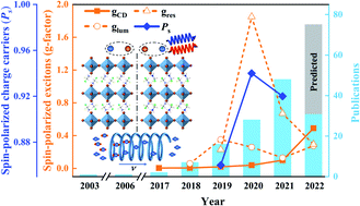

image file: d2ta02207a-p1.tif

Jin Xiao

Jin Xiao graduated from the Hefei University of Technology with a B.E. in 2021. He is a graduate student in the School of Electrical Engineering and Automation at Wuhan University. His current project is the design and synthesis of chiral semiconductors and devices.

image file: d2ta02207a-p2.tif

Haofeng Zheng

Haofeng Zheng received his B.S. degree in Applied Chemistry from the Hefei University of Technology in 2021. He is currently a graduate student in the School of Electrical Engineering and Automation at Wuhan University. His research interest is the design of novel optoelectronic devices and in-depth understanding of their physics.

image file: d2ta02207a-p3.tif

Ruilong Wang

Ruilong Wang is a junior student in the School of Electrical Engineering and Automation at Wuhan University. She joined Prof. Shaocong Hou's group in 2021. Her current interest is data-driven design of semiconductor materials and devices.

image file: d2ta02207a-p4.tif

Yanlong Wang

Yanlong Wang is a junior student in the School of Electrical Engineering and Automation at Wuhan University. He joined Prof. Shaocong Hou's group in 2021. His interest is developing high-throughput, multi-dimensional microscopy and imaging.

image file: d2ta02207a-p5.tif

Shaocong Hou

Shaocong Hou obtained his PhD degree from Peking University in 2014, and then worked for the University of Cambridge (2014–2016), Harvard University (2016–2017) and the University of Michigan (2018–2020). He joined the School of Electrical and Automation, Wuhan University in 2021. His research interests span from fundamental understanding of charge, photon and exciton behaviors to developing next-generation intelligent materials, devices and systems.


1 Introduction

Chirality is defined as two enantiomers that are mirror images of each other and cannot overlap. Chirality exists widely in nature and is closely related to life phenomena, such as our left and right hands, the helical growth of plant rhizomes, the thread of a conch, and copulation in snails. Chiral materials have been widely utilized in asymmetric catalysis,1 optoelectronic devices,2 biomedicine,3 information communication4 and many other fields, promoting the development of human society. Recently, organic–inorganic hybrid metal halides emerged as one of the next-generation optoelectronic materials owing to their large absorption coefficient, long charge diffusion length, high defect tolerance, and adjustable structure. The introduction of chirality into metal halide semiconductors is expected to obtain a new class of chiral semiconducting materials, which are desired in the community.

The research on chiral metal halide semiconductors (CMHSs) started as early as 2003 when Billing et al.5 reported the first single crystal of 1D (S-PEA)PbBr3 (PEA is an abbreviation for α-phenethylamine, also called methylbenzylamine and abbreviated to MBA, and R/S- refers to chiral enantiomers in R/S configurations), followed by another report on a single crystal of a 2D CMHS in 2006.6 In 2017, Ahn et al.7 reported the chiroptical phenomenon in (R/S-MBA)2PbI4, sparking increasing interest in CMHSs. More strategies have been explored to functionalize metal halides with chirality, including incorporating chiral organic molecules into octahedral voids, surface coordinating with chiral organic molecules,8–12 introducing chiral lattice defects,13 designing chiral metasurfaces,14–16 and blending with chiral matrices.17–20 Subsequently, significant nonlinear optics, chirality-induced spin selectivity (CISS), ferroelectricity, and ferromagnetism have been reported in CMHSs.19–23 The development trend of this field in recent years is summarized in Fig. 1.


image file: d2ta02207a-f1.tif
Fig. 1 Schematic diagram of the development in the field of CMHSs. The bar chart represents the total number of papers published in the CMHS field over the years, and the line chart shows the highest value of the anisotropic g-factor over the years. gCD characterizes the ability of circular dichroism (CD), glum characterizes the ability of circularly polarized luminescence (CPL), and gres characterizes the resolution capability of a circularly polarized light photodetector, and the maximum value is 2. Ps characterizes the ability of the CHMS to screen spin state electrons as a spin filter layer, and the maximum value is 1.

2 Chiral crystal structure and electronic band structure

For a typical ABX3 perovskite structure of metal halide semiconductors, A-site cations are filled in the void enclosed by the octahedral cage, coordinating with the [BX6]2− octahedron constituting the inorganic framework to maintain charge and structural stability (Fig. 2a). The A-site organic cation can be the formamidine cation, methylamine cation (MA+), inorganic cation Cs+, etc.; the B position is usually occupied by a transition-metal cation, such as Pb2+ and Sn2+; the X position is occupied by a halogen anion, such as Br−, Cl and I. When the A-site cation is replaced by a chiral organic cation, such as R/S-MBA, which usually has a larger molecular size, the tolerance factor in the octahedral void of the 3D structure cannot be satisfied,24,25 leading to a structural transition to quasi-2D layer,26 2D layer,27 1D chain,28 and 0D cluster29 CMHSs (Fig. 2b–e). So far, more than 30 pairs of chiral organic cations have been introduced into CMHSs. However, the introduction of a small chiral organic cation to achieve a 3D CMHS is only theoretically predicted, and there is no experimental verification yet.30
image file: d2ta02207a-f2.tif
Fig. 2 The structure of a CMHS. (a) ABX3 structure of 3D metal halide semiconductors, reproduced from ref. 32 with permission from Materials Today Nano. (b) 2D layered (R/S-MBA)2PbI4, reproduced from ref. 27 with permission from Angewandte Chemie. (c) quasi-2D laminar (R/S-MBA)2MAPb2I7, reproduced from ref. 26 with permission from American Chemical Society. (d) 1D chain-like (R/S-MBA)PbI3, reproduced from ref. 28 with permission from Angewandte Chemie. (e) 0D cluster-like (R/S-MBA)2Cu4I4, reproduced from ref. 29 with permission from Springer Nature.

In a CHMS, R/S-chiral organic cations coordinate with the inorganic framework through electrostatic interactions, and the inorganic lattice is deformed by asymmetric hydrogen bonding force. Taking (R/S-NEA)2PbBr4 (NEA refers to 1-(1-naphthyl)ethylamine) as an example,31 after the introduction of NEA, three metal halide semiconductors crystallize as [PbBr4]2− octahedral cage corners to form 2D inorganic layers, which are separated by NEA+ interlayer molecules. For rac-NEA, the hydrogen bonding force is symmetric to the Br atom on the axis, that is, two H-bonds of the two nearest –NH3+ adjacent to the Br atom on the axis are symmetric, the inorganic layer causes a symmetrical oblique twist, and the in-plane Pb–Br–Pb bond angles are all 152° (Fig. 3a). For R-NEA, the force on the Br atom on the axis is not symmetrical on both sides. As shown in Fig. 3b, here are two kinds of Br atoms marked in purple/red that are adjacent but in different chemical environments. For the Br atom marked in purple, the –NH3+ and α-CH3 of the interlayer NEA molecules on one side of the inorganic layer both produce hydrogen bonds, and the other side has only hydrogen bonds from –NH3+, which is opposite to the force of its adjacent Br atoms. Due to this asymmetric hydrogen bonding force, the out-of-plane twist of the Br atoms in the horizontal direction occurs. This out-of-plane twist propagates along the b-axis direction, resulting in a helical axis parallel to the b-axis direction. Other Br atoms are marked in red, similar to the purple-marked Br atoms, but with the weaker hydrogen bonding force between Br atoms and NH3+ of NEA+, which causes another helical axis. When the chirality is reversed, the helicity in crystallography is opposite (Fig. 3c), and chirality makes the inorganic layer transform a centrosymmetric structure into a noncentrosymmetric structure, and in-plane Pb–Br–Pb bond angles are 143° and 157°. In (rac-NEA)2PbI4, the dispersion relation of electrons (holes) conserves time-reversal symmetry, i.e. E+(k) = E+(−k), where E± and k represent the sub-bands of electrons (holes) in the lowest conduction band and highest valence band with a spin quantum number s = ±1/2 and the lattice momentum (Bloch wave vector). This transformation of the crystal structure directly leads to the change of the electronic band structure. In achiral materials, the dispersion relation of electrons (holes) conserves time-reversal symmetry (i.e. E+(k) = E(−k)) and space inversion symmetry (i.e. E+(k) = E+(−k)) respectively, and the sub-bands of electron(hole) are doubly degenerate (Fig. 3d).34 In (R/S-NEA)2PbI4, after the introduction of chiral organic molecules into metal halide semiconductors, the noncentrosymmetric structure breaks the inversion symmetry, resulting in spin-degenerate electron sub-bands separated along the k direction (Fig. 3e and f). At the same time, the deformation of the inorganic layer and the alignment of chiral organic molecules induce a large chiral electric field, which leads to a stronger SOC effect and a larger spin splitting. The dispersion relation of spin-split sub-bands is described as:35

image file: d2ta02207a-t1.tif
where ℏ is the reduced Planck constant; m is the effective mass of electrons; αeff = ΔE±/2k0 (k0 is the characteristic momentum) is the spin splitting coefficient, and ΔE± is the energy difference between E+ and E.


image file: d2ta02207a-f3.tif
Fig. 3 The effect of chiral organic molecules on the crystal structure and electronic bands of CMHSs. In-plane views of the [PbBr4]2− inorganic layer of (a) (rac-NEA)2PbBr4; (b) (R-NEA)2PbBr4; (c) (S-NEA)2PbBr4. Reproduced from ref. 31 with permission from Nature Communications. (d) Double spin degenerate sub-bands of electrons and holes for achiral materials. (e) Due to the SOC and noncentrosymmetric properties of CMHSs, the spin-polarized sub-bands (red: s = +1/2; blue: s = −1/2) split in k-space, E+ and E are the energy of the sub-bands of electrons (holes) of s = +1/2. Reproduced from ref. 34 with permission from American Chemical Society. (f) Enlarged view of the yellow square of (e), ΔE± represents the energy difference of the two spin sub-bands at k0. (g) Schematic diagram of the symmetric tilt (left panel) to the asymmetric tilt (right panel) of the [MX4]2− octahedron (M is a metal atom and X is a halogen atom), the symmetric tilt leads to the same M–X–M bond angle and maintains the inversion symmetry, and the antisymmetric deformation breaks the inversion symmetry leading to two different M–X–M bond angles, whose bond angle difference is Δβ = β′ − β; (h) the in-plane and out-of-plane projection angles of β are βin and βout, respectively; (i) the relationship between spin splitting and structural parameters in 2D metal halide semiconductors. Reproduced from ref. 33 with permission from Nature Communications.

Recent studies disclosed that the spin-splitting effect (k0, αeff, and ΔE±) is mainly related to the difference of the adjacent X–Pb–X bond angle Δβ in the inorganic framework (Fig. 3f), and a structural descriptor Δβin of spin-splitting is proposed, which is the difference of projection of β to the horizontal plane formed by coplanar M atoms33 (Fig. 3g and h). This study reveals that spin level splitting and lattice deformation are proportional, and for achiral metal halide semiconductors, lattice deformation may also occur, resulting in circular dichroism (CD) properties. In contrast, the introduction of chiral organic molecules is easier to obtain larger deformation and large CD strength.

3 Chiral effect on excitons and charge carriers

3.1 Spin-polarized excitons

As mentioned earlier, double spin-degenerate sub-bands of electron and hole separate along the k direction, resulting in spin-splitted highest valence band (v+, v) and lowest conductive band (c+, c). This leads to four exciton species, including c+[v with combining macron]+, c+[v with combining macron], c[v with combining macron] and c[v with combining macron]+, where ± denotes s = ±1/2, c and v denote conduction band electrons and valence band holes, respectively, and [v with combining macron]± = [small straight theta, Greek, circumflex]v ([small straight theta, Greek, circumflex] is the time reversal operator). According to the law of optical selection, the interaction with circularly polarized light with spin angular momentum satisfies the conservation of angular momentum, and the angular momentum of excitons is jex = je + jh = ±1, corresponding to c+[v with combining macron]+ and c[v with combining macron] respectively. Due to spin-splitting sub-bands of electrons and holes, the dispersion relation of excitons is also separated along the direction of exciton wave vector K (Fig. 4a and b), and excitons generated under circularly polarized light are called spin-polarized excitons and can be described as:34
image file: d2ta02207a-t2.tif
where M is the total electron–hole effective mass, ω0 is the angular frequency, ℏω0 is the energy of the excitons at Kz = 0, τ = ±1 represents the chirality of the material, and α is the effective SOC intensity of the excitons.

image file: d2ta02207a-f4.tif
Fig. 4 Schematic diagram of spin-polarized exciton generation. (a) and (b) Spin-splitting exciton sub-bands of two CHMS enantiomers. (c) and (d) Enlarged view of the yellow square of (a) to indicate that spin-polarized excitons are the origin of CD and CPL properties respectively. Reproduced from ref. 34 with permission from American Chemical Society.

The dispersion relation of spin-polarized excitons is double parabolic, and the minimum energy of excitons occurs at a finite K = ±K0 = ∓ατMjex, which changes the sign when the helicity jex of circular polarized light or material's chirality τ is reversed. For the excitation process, the optical selection rules require that the exciton wave vector K is equal to the wave vector of the absorbed photon. For photons with wave vector q, the spin-polarized excitons generated by left-handed circularly polarized light (LCP) and right-handed circularly polarized light (RCP) are in different exciton sub-bands (Fig. 4c). There is an energy difference (ΔE) in the excitation process of the two spin-polarized excitons, leading to differences in the absorption of LCP and RCP, which is the intrinsic cause of the CD properties. Similarly, the circularly polarized luminescence (CPL) process is the inverse process of CD (Fig. 4d). In general, spin-polarized excitons are the essential reason for the chiroptical properties in CMHSs.

3.2 Spin-polarized charge carriers

In a chiral medium, the transport of spin charge carriers is affected by the chirality, and two spin charges (s = +1/2 or s = −1/2) are affected differently by the chiral electric field as they pass through the chiral material, resulting in charges with one spin state passing smoothly through (s = +1/2 or s = −1/2 or s = −1/2). This property is also observed in chiral organic molecules, such as helicene molecules,36 DNA molecules37 and so on.

The helical arrangement of chiral organic cations between inorganic layers in CMHSs induces a chiral electrostatic field, which leads to a helical distribution of moving electrons22 (Fig. 5a). The spin charges move along the helical direction and are subjected to the chiral electric field which points to the outward radial direction, and the magnetic field [B with combining right harpoon above (vector)] generated by the current is:

image file: d2ta02207a-t3.tif
where [v with combining right harpoon above (vector)] is the direction of electron motion, c is the speed of light, and [E with combining right harpoon above (vector)]chiral is the chiral electric field.


image file: d2ta02207a-f5.tif
Fig. 5 Schematic diagram of the spin-polarized charges. (a) The charge with an opposite spin is affected by the magnetic field [B with combining right harpoon above (vector)] when passing through the medium with opposite chirality. [S with combining right harpoon above (vector)] and [v with combining right harpoon above (vector)] are the spin and motion directions of the charge. Reproduced from ref. 22 with permission from Springer Nature. (b) Schematic diagram of spin-polarized charge generation through a chiral medium, which is controlled by the chirality of the medium.

Because the charges have a spin-dependent magnetic moment, when the charges with [v with combining right harpoon above (vector)] pass through the chiral electric field within the CMHS, it is subject to the [B with combining right harpoon above (vector)], and charges with the same spin direction as [B with combining right harpoon above (vector)] pass smoothly, while the transport process of the charge with the opposite spin direction as [B with combining right harpoon above (vector)] is hindered, and the direction of [B with combining right harpoon above (vector)] is affected by the helicity of the CMHS38 (Fig. 5b). The existence of spin-polarized charges brings about the capacity of controlling the spin of charges, which is the fundament of the spintronic devices.

4 Optical and electrical properties

The unique crystal structure and band structure of CHMSs promise novel macroscopic material properties. Spin-polarized excitons have an anisotropic response to circularly polarized light, including CD and CPL; spin-polarized charges lead to spin-selective charge transport in CMHSs, namely the CISS effect; noncentrosymmetric structure may lead to the existence of nonlinear optics and ferroelectricity.

In the following, we will introduce the influence of chirality on macroscopic properties in two parts. One is optical properties, including CD, CPL and nonlinear optics, and the other is electrical properties, including the CISS effect, ferroelectricity and ferromagnetic.

4.1 Optical properties

4.1.1 CD properties. The CD strength of materials is proportional to the rotational strength (R):39
CD ∝ R = Im[〈ψs|[small mu, Greek, circumflex]|ψj〉〈ψs|[m with combining circumflex]|ψj〉] = Im[[small mu, Greek, circumflex]sj[m with combining circumflex]js]
where ψs and ψj are the ground and excited state wave functions, and [small mu, Greek, circumflex]sj and [m with combining circumflex]js are the transition electric and magnetic dipole moments.

The premise for the CD intensity generation is that R ≠ 0, i.e. [small mu, Greek, circumflex]sj ≠ 0, [m with combining circumflex]js ≠ 0, and the angle between them is parallel or antiparallel, and CMHSs with chiral point groups that meet the above conditions will exhibit CD intensity.

The CD properties of chiral materials are generally characterized by CD spectroscopy, which is similar to UV-Vis absorption spectroscopy, except that it measures the absorbance of a material to both LCP and RCP at each wavelength. The ordinate of CD spectroscopy is represented by ellipticity (θ), the unit is mdeg, and the relationship between θ and absorbance (A) is:

image file: d2ta02207a-t4.tif
where ΔA = ALAR, the difference between the absorbance of LCP and RCP.

The intensity of CD spectroscopy (θ) is significantly affected by the orientation and thickness of the crystal plane of the sample on the substrate. Therefore, the evaluation of the anisotropic of absorption is usually expressed by the g-factor, to exclude the influence of external conditions including film thickness, crystal plane orientation, etc. The g-factor is represented as gCD (which is also expressed by gabs in some literatures) in CD properties, which is defined as:

image file: d2ta02207a-t5.tif
AL and AR are the absorbance of LCP and RCP, respectively, and the value of gCD is between −2 and 2.

Although the research on CMHSs started in 2003, the study of CD properties brought about by chirality was first reported in 2017.7 Ahn et al.7 found that (R/S-MBA)2PbI4 has different absorption for LCP and RCP according to its chirality, namely CD. The CD signals of (R-MBA)2PbI4 and (S-MBA)2PbI4 are opposite (Fig. 6a). There is CD near the exciton peak of (R/S-MBA)2PbI4 at 501 nm and a zero-crossing and opposite CD peak after the exciton peak, which is far away from the CD peak of R/S-MBA (below 260 nm) confirming the CD peak from the inorganic layer and chirality transfer from organic molecules to (R/S-MBA)2PbI4. And the CD nature of CMHSs can be regulated by the structure compositions40–43 and dimensions.44,45


image file: d2ta02207a-f6.tif
Fig. 6 (a) CD and absorption spectra of (R-MBA)2PbI4 and (S-MBA)2PbI4 thin films at 20 wt%; the inset shows a schematic diagram of the CD spectroscopy test. Reproduced from ref. 7 with permission from Royal Society of Chemistry. Circularly polarized light-sensitive PL spectrum of (b) (R-MBA)2PbI4 and (c) (S-MBA)2PbI4 under a 473 nm laser at 77 K. Reproduced from ref. 49 with permission from American Chemical Society.

In the composition of CMHSs, the most significant effect of chirality is the species of chiral organic cations, that is, substituent groups of the chiral center. The substituent group of the chiral center mainly affect the chirality of CMHSs through asymmetric hydrogen bonding force, but there are also intermolecular forces between chiral organic molecules, which affect the arrangement of the chiral organic molecules in the interlayer, thereby indirectly affecting the hydrogen bonding force between the inorganic framework and the chiral organic molecules, thereby affecting the chirality of the CMHS. Specifically, the substituent groups on the chiral center affect the chirality of CMHSs mainly in three ways. Firstly, compared with non-aromatic chiral organic cations, CMHSs composed of aromatic chiral organic cations have higher chirality.28 And the more aromatic rings, the higher the chirality. This is likely due to the intermolecular interaction caused by the π bond between the aromatic chiral organic cations, making the chiral organic cations arranged in the interlayer orderly and then inducing stronger chirality transfer.46 Second, the chiral center located on the α or β position of the amine chain will also affect the chirality. The chiral center located on the α position has stronger chirality than the chiral center at the β position, which may be attributed to the hydrogen bonding interaction, and the asymmetry of the hydrogen bonding interaction between the chiral organic cation with the chiral center at the α-position and the inorganic framework may be stronger. Finally, the substituents on the benzene ring also affect the chirality. The introduction of functional groups on the benzene ring may bring about other electrostatic forces, thereby changing the arrangement of organic molecules and changing the chirality of CMHSs.40 Besides chiral organic cations, the composition of the inorganic framework not only changes the band gap of CHMSs, but also affects the chirality, which may be related to the steric hindrance effect between inorganic frameworks and the hydrogen bonding force between halogens and chiral organic cations.

In addition to the composition of organic anions, the structure of CHMSs also has an important impact on CD. In the process of CHMS structure transformation from 2D to 1D to 0D, the stronger the influence of chiral organic molecules on the inorganic framework, the stronger the chirality of the overall structure. According to the highest value of gCD over the years as shown in Fig. 1, the gCD of 2D (R/S-MBA)2PbI4 only reached 0.005,7 and the gCD of a 2D Br-based CMHS is 0.006.44 When the structure of a 2D CMHS is transformed to lower dimensions, the gCD of 1D (R-MBA)PbI3 and (R/S-NEA)PbI3 is 0.02 and 0.04 respectively.28,46 As the structure of CMHS is further transformed from 1D to 0D, the reported gCD of 0D (R/S-MBA)2CuCl4 reaches 0.1.47 Recently, a chiral superstructure based on a 3D perovskite has achieved a gCD of 0.49.48

4.1.2 CPL properties. As emission is the reverse process of absorption, CPL can also be regarded as the reverse process of CD, which is produced by the transition of spin-polarized excitons back to the ground state. Similar to the gCD of the CD nature, the g-factor of the CPL properties is expressed by glum:
image file: d2ta02207a-t6.tif

Among them, IL and IR represent the emission intensity of LCP and RCP emitted by the chiral material, and the range of glum is −2 to 2. It is also expressed by the degree of photoluminescence polarization (DP), DP = ILIR/IL + IR = 1/2glum.

Sargent's group44 discussed the CPL properties of quasi-2D CMHS—(R/S-MBA)2MA0.2Cs0.8Pb2Br7, which exhibits magnetic field-regulated CPL capability and DP = ±3% (under B = 0) at 3 K, and a series of quasi-2D CMHSs and investigated their CD and CPL change with the number of inorganic layers (n). The experiment found that with the increase of the number of inorganic layers, the 2D structure transforms into 3D, the crystal defects become fewer, and the nonradiative recombination competitiveness reduces, which makes the photoluminescence quantum yield (PLQY) and PL intensity increase, but the proportion of chiral organic molecules decreases as n increases, and the chirality and the CD intensity decrease. In contrast, as n decreases, the PLQY and PL intensity decrease, and the chirality and the CD intensity increase.44,45 According to Fig. 1, the highest CPL efficiency so far has been achieved in 2D CMHSs,49 which may be due to the relatively high PLQY and CD of the 2D structure, resulting in relatively higher CPL efficiency. The reported average DP of (R-MBA)2PbI4 and (S-MBA)2PbI4 at 77 K was 10.1% and −9.6% respectively, and the highest DP of (S-MBA)2PbI4 can reach 17.6%, obtained from the circularly polarized light-sensitive PL spectrum (Fig. 6b and c).49 Notably, there is almost no CPL emission at room temperature, which can be attributed to the depolarization of excitons returning to the ground state.

An aqueous phase synthesis method50 was used by adding a small proportion of MA+ during the synthesis process, and MA+ does not change the composition and structure of (R/S-MBA)2PbI4, but induces (R/S-MBA)2PbI4 to produce a CPL signal at room temperature, which may be attributed to the passivation effect of the MA+ additive and the average DP of (R-MBA)2PbI4 and (S-MBA)2PbI4 was 13.7% and 11.4%.27 The CPL capability of (R/S-MBA)2PbI4[thin space (1/6-em)]27,51 and (R/S-1-(4-bromophenyl)ethyl-amine)2PbI4[thin space (1/6-em)]52 reaches DP > 10% at room temperature, but there is still plenty of room for DP to be improved up to the theoretical maximum DP value of 1.

The CPL efficiency of CMHSs is mainly determined by PLQY and the luminescence anisotropy factor (glum). For CMHSs, in order to obtain larger absorption and emission anisotropy, the crystalline structure of CMHSs changes from 3D to 2D or 1D, while resulting in a high density of lattice defects and phonon-coupling effects, and thus strong nonradiative recombination significantly reduces their PLQY. Therefore, there is a trade-off between high PLQY and high glum at the same time, which is still under intense investigation. Nonetheless, there are generally three potential methods to overcome the trade-off between PLQY and glum: (1) exploring the synergistic effect of chiral ligands and highly emissive metal halide semiconductor nanocrystals;1 (2) enhancing the chiral transfer from a low-dimensional CMHS to a highly emissive 3D CMHS via, such as, heterojunctions; (3) experimental synthesis of 3D chiral metal halide semiconductors.

4.1.3 Nonlinear optics. The relationship between the electric polarization density P(t) (that is, the electric dipole moment per unit volume) and the electric field E at time t can be expanded by the Taylor series:
P(t) = ε0(χ(1)E(t) + χ(2)E2(t) + χ(3)E3(t) + …)

Under the excitation of a weak light field, nonlinear term can be ignored, which is a linear optical property, including CD property and CPL property. However, under the excitation of a strong light field, such as a high-power laser, its nonlinear response cannot be ignored, that is, a nonlinear optical phenomenon occurs. According to the number of photons involved in the process of nonlinear optical phenomena, they are divided into second-order nonlinear processes (involving two photons), third-order nonlinear processes, and so on.54

The noncentrosymmetric structure of a CMHS makes it more favourable to study nonlinear optical phenomena.53,55–59 The second harmonic generation (SHG) effect in CMHSs was first reported in 2018.53 In this case, 2D (R/S-MPA)1.5(DMSO)0.5PbBr3.5 nanowires (MPA refers to β-methylphenethylamine) under the irradiation of a long-wavelength laser emit short-wavelength SHG light, whose frequency is twice that of the pumping laser (Fig. 7a). The slope of SHG intensity versus laser power is 2.0 (Fig. 7b), which proves that this process involves two incident photons. In addition, based on the test system (Fig. 7c), the anisotropic SHG response of the sample to linearly polarized light and circularly polarized light is tested through λ/2 and λ/4 wave plates. For example, (R/S-MPA)1.5(DMSO)0.5PbBr3.5 nanowires exhibited that the SHG signal generated under the excitation of linearly polarized light is related to the direction of the polarization plane of linearly polarized light (Fig. 7d). The closeness of the horizontal (P) and vertical (S) detector signals indicates that the SHG has only circularly polarized signals (Fig. 7e). The polarization of the SHG signal generated under the illumination of circularly polarized light is represented by SHG-CD (it represents the strength of the circular dichroism of the produced SHG signal), and the SHG-CD of (R/S-MPA)1.5(DMSO)0.5PbBr3.5 was (61.9 ± 0.1)% and (74.0 ± 0.1)% for the P and S detectors (Fig. 7e), respectively. Apart from the SHG effect, the two-photon absorption effect in CMHSs can detect near-infrared light60 and the two-photon absorption-based upconverted circularly polarized luminescence found in chiral metal halide semiconductor nanocrystals.61 The chiroptical properties of CMHSs can realize the regulation of polarized light through nonlinear optics, which broaden the application range of nonlinear optical properties. To achieve stronger nonlinear optics, more precise control of the composition, size, and external conditions of CMHSs as well as a deeper understanding of the generation mechanism of CMHS nonlinear processes is required.59,62


image file: d2ta02207a-f7.tif
Fig. 7 SHG effect in a CMHS. (a) SHG signal intensity as a function of laser wavelength. (b) The SHG signal intensity varies with the laser power. (c) Schematic diagram of SHG signal testing, λ/2 and λ/4 waveplates are used to test SHG signals generated by linearly polarized light and circularly polarized light, respectively. (d) SHG signal detected by the P and S analyzers as a function of the linear polarization angle of the linearly polarized light, which is adjusted by rotating the λ/2 waveplate. (e) The SHG signal detected by the P and S analyzers as a function of the rotation angle of the λ/4 waveplate, which is LCP when the rotation angle is 45° and 225°, and RCP when the rotation angle is 135° and 315°, as indicated by the circled arrows. Reproduced from ref. 53 with permission from American Chemical Society.

4.2 Electrical properties

4.2.1 Chirality-induced spin selectivity. The first discovery of the CISS effect in CMHSs was made in 2018; Lu's group63 deposited a layer of (R/S-MBA)2PbI4 on fluorine-doped tin oxide (FTO) substrates. The CISS effect of (R/S-MBA)2PbI4 was characterized by magnetic conductive-probe atomic force microscopy (mCP-AFM), and charge carriers with a specific spin direction are injected through the ferromagnetic tip, whose spin direction is controlled by the direction of the magnetic field applied perpendicular to the ferromagnetic tip (Fig. 8a). By controlling the direction and bias of the applied magnetic field on the ferromagnetic tip, the relationship between material chirality and spin-polarized charge is studied (Fig. 8b and c). The degree of the spin-polarized the charges (Ps) through the (R/S-MBA)2PbI4 layer is defined as:
image file: d2ta02207a-t7.tif
where I+ and I are the measured currents through the film when a vertically upward and downward magnetic field is applied to the ferromagnetic tip respectively, and the range of Ps is −1 to 1.

image file: d2ta02207a-f8.tif
Fig. 8 Test of the spin polarization efficiency of charges through a CMHS. (a) The mCP-AFM test system, and the spin direction of the charges injected into the film is controlled by the direction of the magnetic field applied on the ferromagnetic tip. The polarization current of (b) (R-MBA)2PbI4; (c) (S-MBA)2PbI4; (d) (R-MBA)2SnI4; (e) (S-MBA)2SnI4 as a function of voltage, and Tipup, Tipdown and TiP0 represent the applied magnetic field on the ferromagnetic tip vertically upward, downward, and no applied magnetic field, respectively. Reproduced from ref. 63 with permission from American Association for the Advancement of Science and ref. 43 with permission from American Chemical Society.

With the application of −2 V bias, the spin-polarized charges pass through the (R/S-MBA)2PbI4 film and show a high spin-polarization effect, and the Ps of (R-MBA)2PbI4 and (S-MBA)2PbI4 reaches +86% and −84% (Fig. 8d and e), which are much higher than the Ps of chiral organic monolayers36,37 (usually 30–50%). 1D (R/S-MBA)PbBr3 also exhibits spin-polarized efficiencies higher than 90% at −1 V.64 In addition to Pb-based CMHSs, lead-free CMHSs such as (R/S-MBA)2SnI4 also have a stronger chiral induced SOC effect due to their larger lattice deformation, which display stronger charge spin polarization, and the Ps of (R-MBA)2SnI4 and (S-MBA)2SnI4 is +94% and −93% respectively, which are close to 1 under −1 V bias.43 The Ps of (R/S-MBA)CuX4 (X = Cl, Br) of the 0D clusters is above 90% under −2 V bias.65

Additionally, characterizing the CISS effect by the magneto-optical Kerr effect can also be studied,66 and the accumulation of spin charges was measured by using the magneto-optical Kerr angle, which also confirmed the spin polarization of charges in the CMHS.

Compared with self-assembled chiral organic molecule monolayers,36 CMHSs have no limit of monolayers and achieve a spin polarization efficiency close to 1, and the direction of spin polarization is controlled by the chirality of CMHSs. These fully illustrate the application potential of CMHSs to control the spin.

4.2.2 Ferroelectric. Ferroelectric means that in the absence of an applied electric field, the orientation of dipole moments in a material leads to its characteristic of spontaneous polarization, and the polarization properties are controlled with an applied electric field. The three most important parameters of ferroelectricity are the saturation polarization (the maximum value of the polarization of the material), the coercive electric field (when the polarization is 0, the strength of the external electric field) and the Curie temperature (Tc, also known as the transition temperature; above Tc the ferroelectricity disappears and the material becomes paraelectric). For nearly a century, ferroelectrics have been widely used in memory elements, sensors, and capacitors.67 Ferroelectrics are a subclass of pyroelectrics, which is contained within piezoelectric. The crystal forms of ferroelectrics should belong to ten polar point groups (C1, C2, Cs, C, C4, C, C3, C, C6, and C);68 if the chiral point group structure of CMHSs belongs to the ten polar point groups, it is expected to exhibit ferroelectricity (C1, C2, C3, C4, and C6). In recent years, with the discovery of CMHSs, various CMHS ferroelectrics, such as free-metal 3D perovskite (R/S-3-ammoniopyrrolidinium/3-ammonioquinuclidinium)NH4Br3,69 2D (R/S-1-(4-chlorophenyl)ethylamine)2PbI4[thin space (1/6-em)]70 and (R/S-N-(1-phenylethyl)ethane-1,2-diaminium)PbI4,71 1D (R/S-3-F-pyrrolidinium)MnCl3[thin space (1/6-em)]72 and (R/S-3-F-pyrrolidinium)CdCl3,73 all exhibited larger saturation polarization and higher transition temperatures. Meanwhile, ferroelectrics must have piezoelectric properties, and there are recent reports on the piezoelectricity of (R/S-1-(4-bromophenyl)ethylamine)2PbI4.52 CMHS ferroelectrics possess not only ferroelectricity, but also semiconducting properties103 (Fig. 9a). The ferroelectric properties of (R/S-cyclohexylethylamine)PbI3 are clearly seen from the PE hysteresis loop with a saturation polarization of 0.03 μC cm−2 (Fig. 9b). By combining its ferroelectric and semiconducting properties to test the typical switching diode effect (Fig. 9c), the photocurrent direction of the device depends on the previous polarization direction (controlled by the direction of pre-biasing voltage), which is the result of band bending caused by previous ferroelectric polarization (Fig. 9d). For example, when the direction of the pre-biasing voltage switches, the direction of the photocurrent is reversed.
image file: d2ta02207a-f9.tif
Fig. 9 Ferroelectricity and switching diode effect tests of (R/S-cyclohexylethylammonium)PbI3. (a) Design principle of (R/S-cyclohexylethylammonium)PbI3 ferroelectrics, which are not only ferroelectric but also have chiral and semiconducting properties. (b) PE hysteresis loop of (R/S-cyclohexylethylammonium)PbI3. (c) Switchable diode effect of (R/S-cyclohexylethylammonium)PbI3: photocurrent measured without bias after applying 10 V and −10 V bias for 200 s. (d) Band structures in the device under zero, positive, and negative bias applied before testing. Reproduced from ref. 103 with permission from American Association for the Advancement of Science.

In addition to the phenomenon of the PE hysteresis loop, the spontaneous polarization characteristic of ferroelectricity also brings about the bulk photovoltaic effect in CMHS,75 facilitating the realization of self-powered photodetection. CMHS ferroelectrics expand the scope of ferroelectric materials, provide a good platform for the study of ferroelectricity, and are expected to solve the problem of low Tc of ferroelectrics. Furthermore, ferroelectricity combined with chirality and semiconducting properties is beneficial to studying the circularly polarized photovoltaic effect76 and realizing chirality and electric field-controlled switching devices.103

4.2.3 Ferromagnetic. Except for ferroelectric properties, ferromagnetic properties have also been found in chiral metal halide semiconductors.77,78 In 2D (R-MPA)2CuCl4, (S-MPA)2CuCl4 and (rac-MPA)2CuCl4,77 the magnetization properties change from ferromagnetic to paramagnetic with increasing temperature (Fig. 10a), and a clear H–B hysteresis loop at T = 2 K is observed in all cases (Fig. 10b–d). The magnetization strength reaches a saturation value of 12.5 emu g−1 at an applied magnetic field of 2500 Oe, but the magnetization properties disappear when the temperature is higher than Tc. Combining the chirality and ferromagnetism of (R/S-MPA)2CuCl4, its magnetic-chiral circular dichroism (MChD) was studied, which exhibits opposite signals in opposite chiral enantiomers (Fig. 10e). The absorption g-factor (gMChD) for MChD is defined as:
image file: d2ta02207a-t8.tif
where A = (ALAR)/2, AL and AR are the absorbances for LCP and RCP in the absence of a magnetic field) and B↑↑k and B↑↓k represent the external magnetic field and the wave vector k of light that are parallel and antiparallel respectively.

image file: d2ta02207a-f10.tif
Fig. 10 Ferromagnetism and MChD of (R/S-MPA)2CuCl4. (a) Magnetization of (R-MPA)2CuCl4, (S-MPA)2CuCl4, and (rac-MPA)2CuCl4versus temperature under an applied 100 Oe magnetic field. Hysteresis loops of (b) (R-MPA)2CuCl4; (c) (S-MPA)2CuCl4; (d) (rac-MPA)2CuCl4 at 2, 5, 10, and 15 K. (e) MChD tests (two-dimensional perovskite chiral ferromagnets) of (R-MPA)2CuCl4 and (S-MPA)2CuCl4 at 2 K. Reproduced from ref. 77 with permission from American Chemical Society.

The gMChD of (R-MPA)2CuCl4 and (S-MPA)2CuCl4 is 0.51 T−1 and 0.59 T−1, respectively, which are much larger than that of the previously reported metal organic complex of Eu (5 × 10⁻³ T−1).79

The future of the development of magneto-optical devices based on the high MChD properties of chiral metal halide semiconductor materials using the synergistic effect of chirality and ferromagnetism is prospective. Since CMHSs have ferroelectric and ferromagnetic properties, they are expected to be a research platform for multiferroics.

5 Spin-polarized excitonics and electronics

This chapter divides the new applications into excitonics and electronics according to the spin-dependent behaviours of excitons and charge carriers in CMHSs.

5.1 Circularly polarized photodetectors

Traditional detectors need linear polarizers and quarter waveplates to detect circularly polarized light, which is not facile to miniaturization and integration, and signal attenuation is inevitable in the process of detecting signals. As a consequence, the direct detection of circularly polarized light through the circularly polarized light sensitivity of chiral semiconductors to construct circularly polarized photodetectors (CPDs) is the trend. Compared with other CPDs based on other chiral systems, an emerging CMHS-based CPD has been developed rapidly in recent years.

The quality parameters of CPDs are similar to those of non-polarized photodetectors, including photoresponsivity (R), response time, specific detectivity (D*), etc.80 The difference between CPDs and traditional photodetectors is that they generate different detection signals for LCP and RCP, that is, the ability to distinguish circularly polarized light. The g-factor of photoresponsivity to circularly polarized light is expressed by gres, which is defined as:

image file: d2ta02207a-t9.tif
where RL and RR are the photoresponsivity of the detector under LCP and RCP respectively, and the range of gres is −2 to 2.

According to the principle of light detection, CHMS-based CPDs are divided into four categories, including photoconductors, photodiodes, phototransistors and full Stokes photoconductors.

5.1.1 Photoconductors. Photoconductive CPDs separate spin-polarized excitons under an external electric field.26,81 In 2019, Tan's group28 first reported a CPD based on a CHMS by using spin coating to deposit a layer of an (R/S-PEA)PbI3 polycrystal film on a quartz glass substrate and then deposited on a metal Au electrode with a channel length of 10 μm (Fig. 11a). Under the excitation of CPL at 395 nm with a power of 5.0 μW cm−2, the peak responsivity is 0.12 A W−1, gCD is 0.02, and the resolution capability of circularly polarized light gres is 0.1 (Fig. 11b and c). The corresponding D* calculated by using image file: d2ta02207a-t10.tif (A is the effective area of the detector) is 7.1 × 10¹¹ Jones. The CPD based on (R/S-PEA)PbI3 has a lower resolution of circularly polarized light than a CPD using plasmonic materials (gCD is 0.9, and gres is 1.09 calculated from an RL/RR of 3.4[thin space (1/6-em)]83). However, the R is greater than that of plasmonic photodetectors (2.2 mA W−1), and meanwhile the development of a CPD based on a CMHS has just started. In 2020, Ishii et al.46 reported a CPD based on an (R/S-NEA)PbI3 thin film, whose CD intensity can reach 3200 mdeg near the exciton peak at 395 nm and a gCD of 0.04, which was previously reported to be twice that of (R/S-PEA)PbI3. The thin-film CPD based on (R/S-NEA)PbI3 showed excellent performance, and the R was 0.28 A W−1 under CPL, and it exhibited a very large gres of 1.85 (calculated based on an RL/RR of 3.4), which is close to the theoretical maximum value (the maximum of |gres| is 2). Although a thin-film CPD has the advantage of being simple to prepare, the polycrystal thin films prepared have grain boundaries, high defect state density and impurity concentration, resulting in small photocurrents and poor responsiveness. The (R/S-MPA)2MAPb2I7 single crystal has extremely low defect state density Ntrap (4.3 × 1010 cm−3) and free charge density Nc (1.5 × 108 cm−3), which is the basis for high-performance photodetection performance.26 Two conductive electrodes were deposited on (R/S-MPA)2MAPb2I7 single-crystal microplates (Fig. 11d). The (R-MPA)2MAPb2I7 single crystal detector has a gIph (equal to gres, g-factor of photocurrent) of 0.11, a maximum R of 3.8 A W−1, and a maximum detection capability of D* of 1.1 × 10¹² Jones (Fig. 11e and f).
image file: d2ta02207a-f11.tif
Fig. 11 CMHS-based circularly polarized photodetectors. (a) Schematic diagram of the CPD-based (R/S-PEA)PbI3 polycrystal film. (b) Responsivity and photoconductive gain of the (R/S-PEA)PbI3 photodetector under LCP and RCP illumination at 365 nm, 395 nm, 430 nm and 530 nm. Grey and blue areas indicate the difference in responsivity and photoconductive gain under LCP and RCP illumination. (c) Wavelength-dependent gres spectrum. Reproduced from ref. 28 with permission from Angewandte Chemie. (d) (R/S-MPA)2MAPb2I7 single crystal detector structure and test diagram. (e) IV curves of the (R-MPA)2MAPb2I7 single crystal detector under the illumination of 532 nm with power fixed at 0.23 mW cm−2 of RCP and LCP. (f) The relationship between detectivity and EQE and light intensity under 10 V bias. Reproduced from ref. 26 with permission from Angewandte Chemie. (g) Schematic diagram of the (R-MPA)2PbCl4/Si heterojunction detector. (h) Photocurrent responses of (R-MPA)2PbCl4/Si heterojunction detectors under LCP and RCP illumination. (i) Band diagram of the (R-MPA)2PbCl4/Si heterojunction. When charges are separated at the interface, electrons in specific spin states are transferred from (R-MPA)2PbCl4 to Si, spin-polarized electrons resulting in a stronger anisotropy for the detection of circularly polarized light. Reproduced from ref. 82 with permission from Small.
5.1.2 Photodiodes. Spin polarized excitons are separated by a built-in electric field originating from the heterojunction in the photodiode architecture.82,84 As a low-dimensional metal halide semiconductor, a CMHS has a large exciton binding energy, which leads to a high exciton recombination rate and difficulty in the separation of photogenerated charges. Recently, it was found that a CMHS-based heterojunction has interlayer exciton coupling85 and controlled valley polarization.86 A heterojunction based CPD combined a built-in electric field and CISS effect, which is expected to show a higher resolution of circularly polarized light. The (R-MPA)2PbCl4/Si heterojunction82 has a defect density of states (3.9 ± 2.2) × 1010 cm−3 comparable to that of the (R-MPA)2PbCl4 single crystal ((2.0 ± 1.8) × 1010 cm−3), and has a shorter PL lifetime (3.2 ns) than the (R-MPA)2PbCl4 single crystal, indicating that the (R-MPA)2PbCl4/Si heterojunction has a lower spin-polarized exciton recombination rate. In the CPD based on (R-MPA)2PbCl4/Si (the device structure in Fig. 11g) with applied 0 V bias, an anisotropic circularly polarized light response is generated (Fig. 11h), and the g-factor of the short circuit current (gSC, equivalent to gres) is 0.4. The heterojunction based CPD has higher resolution capability of circularly polarized light than the general CMHS thin film or single crystal CPD, which is caused by the charge separation at the heterojunction and the CISS effect in (R-MPA)2PbCl4 (Fig. 11i).
5.1.3 Phototransistors. The photogating effect exists in field effect transistors, which regulates the source-drain current by adjusting the channel conductance (gate-source voltage). The heterojunction of chiral (R/S-MBA)2CuCl4 and a p-type single-walled carbon nanotube semiconductor as a high-mobility transport channel applied to field effect transistors47 demonstrates detection capability of circularly polarized light. Combining the stronger CD of 0D (R/S-MBA)2CuCl4 (gCD ∼ 0.1) and the CISS effect in the heterojunction, this CPD exhibits competitive circularly polarized light detection capability with gres up to 0.21, higher photocurrent response with R up to 452 A W−1, and a low working voltage of 0.01 V. The current amplification effect based on field effect transistors is expected to obtain larger photocurrent responsiveness, promising to apply in integrated circuits.
5.1.4 Full Stokes photoconductors. The polarization state of monochromatic light can be expressed by the coordinates within the Poincaré sphere. The vector from the centre to the point of the circle is called the Stokes vector, and the coordinates of the point are called the Stokes parameters, including S0, S1, S2, and S3[thin space (1/6-em)]87 (Fig. 12a). For elliptically polarized light, there is a corresponding point on the surface of the Poincaré sphere indicating the polarization state, where linearly polarized light and circularly polarized light are special cases of elliptically polarized light (Fig. 12b). S0 = I, S1 = IxIy, S2 = Iπ/4I−π/4, and S3 = ILIR, where I is the total intensity, and Ix, Iy, Iπ/4, and I−π/4 are the components of the linearly polarized part of the polarized light along the x, y, π/4 and −π/4 directions; IL and IR denote the components of the LCP and RCP of the polarized light.88 The Stokes parameter detection of polarized light is important in photography,89 imaging,90 and spectral measurement.91 To achieve full Stokes parameter detection, devices are necessary to be sensitive to both linearly polarized light and circularly polarized light. The conventional method to achieve full Stokes parameter detection of polarized light is through λ/4 waveplate and linear polarizer, then using photodetector for detection, which is complicated, time-consuming and the auxiliary of optical devices is not conducive to its miniaturization. Recently, a single-crystal nanowire array detector based on (R/S-MBA)2PbI4 combined the circularly polarized light photosensitivity of (R/S-MBA)2PbI4 with the linearly polarized light anisotropy of nanowire arrays to enable the detection of full Stokes parameters (Fig. 12c).87 The single-crystal nanowire arrays have structural anisotropies that make them sensitive to linearly polarized light with a linear polarization ratio of about 1.6 (Imax/Imin) (Fig. 12d), and a maximum R of 47.1 A W−1 and D* of 1.24 × 10¹³ Jones, which is higher than that previously reported for CPDs that are one or two orders of magnitude greater in responsiveness, with a maximum gres of 0.15. The theoretical values of photocurrents in various polarization states were predicted based on the absorption coefficient, and the comparison with the experimentally measured values showed good agreement, which proved its capability of full Stokes parameter detection (Fig. 12e).
image file: d2ta02207a-f12.tif
Fig. 12 Full Stokes parameters and full Stokes detector. (a) The various Stokes parameters of elliptically polarized light are expressed in Poincaré spherical coordinates. The angle between the Stokes vector and the S1S2 plane is 2θ, and the angle between its projection on the S1S2 plane and S1 is 2ϕ. (b) The plane of polarization and the ellipticity parameters of elliptically polarized light correspond to the spherical coordinates of the Stokes vector, and the correspondence between the ellipticity parameters and the Stokes parameters is shown on the blue arrow. (c) Schematic diagram of the Stokes photodetector based on (R/S-MBA)2PbI4 single-crystal nanowire arrays. (d) Variation of photocurrent with the linear polarization angle of (R/S-MBA)2PbI4 single-crystal nanowire arrays under 119.5 mA W−1 and 505 nm linearly polarized light illumination. (e) The experimentally measured and theoretically derived values under illumination with different polarized light, and the dots and solid lines represent the experimental and theoretical values, respectively, and the experimental and theoretical values have been normalized. Reproduced from ref. 87 with permission from American Chemical Society. (f) Schematic diagram of the structure and measurements based on the (R/S-MBA)2PbI4 single-crystal microplate detector with the polarization direction of the incident light adjusted by λ/2 and λ/4 waveplates. (g) Stokes parameters of incident light (S1, S2, and S3) for nine different polarization states measured using a polarization analyzer (black circle) and an (R/S-MBA)2PbI4 single crystal microplate detector. Reproduced from ref. 92 with permission from small.

Following this work, Li's group92 also reported a full-Stokes photoconductor based on an (R/S-MBA)2PbI4 single-crystal (Fig. 12f), which utilizes the inherent linear anisotropies in the ac-plane of 2D (R/S-MBA)2PbI4 to achieve sensitive detection of linearly polarized light, thus achieving the detection of full Stokes parameters. The accuracy ofS1 and S2 is high when the experimental values are compared with the input values, but the accuracy of S3 parameter detection is low (Fig. 12g). This is because the (R/S-MBA)2PbI4 polycrystal film has a poor resolution for circularly polarized light, and the oblique illumination of incident light leads to a further decrease in the sensitivity of circularly polarized light.

5.2 Spintronics

Conventional electronic components generally control the movement of charge carries, but not the spin of charges. The traditional method of controlling the spin of charges is to use ferromagnetic contacts and apply external magnetic field conditions to achieve spin control of charges. The CISS effect of CMHSs enables the control of electron spin by chirality, thus achieving the control of electron spin without an external magnetic field or ferromagnetic contacts. In recent years, spintronic devices such as spin valves and spin LEDs derived from the CISS effect of CMHSs have been reported.
5.2.1 Spin value devices. In spin valve device based on 2D (R/S-MBA)2PbI4,63 the applied single ferromagnetic contact and (R/S-MBA)2PbI4 film replace the two ferromagnetic contacts of the conventional spin valve, and (R/S-MBA)2PbI4 is sandwiched between the ferromagnet electrode and nonmagnetic electrode (indium tin oxide: ITO), as shown in the inset in Fig. 13a. The magnetoresistance (MR) of the spin valve based on (R/S-MBA)2PbI4 is related to the applied external magnetic field, and the MR is defined as:
image file: d2ta02207a-t11.tif
where R(0) is the spin valve resistance before the application of the magnetic field and R(B) is the spin valve resistance under the applied magnetic field B in the perpendicular device direction.

image file: d2ta02207a-f13.tif
Fig. 13 Spin-valve devices based on (R/S-MBA)2PbI4 and thickness-dependent MR study. MR response of (a) (R-MBA)2PbI4; (b) (S-MBA)2PbI4; (c) (rac-MBA)2PbI4 with applied vertical magnetic field B, and the device structure is shown in the inset; (d) the thickness-dependent MR response is decomposed into two components, the spin selection effect in the chiral organic layer (blue triangle) and the spin-deposition effect in the inorganic layer (red circles) contribution to MR response; (e) schematic of spin selective charge transport through 2D (R/S-MBA)2PbI4. Reproduced from ref. 63 with permission from American Association for the Advancement of Science.

The MR response of the spin valve based on (R/S-MBA)2PbI4 shows that the MR signal of the spin valve reverses with the inversion of the magnetic field (Fig. 13a and b). Moreover, the inversion of the external magnetic field causes the magnetization direction of the NiF ferromagnetic contacts to change, thus reversing the MR of spin charges. (R-MBA)2PbI4 and (S-MBA)2PbI4 have opposite MR directions, while (rac-MBA)2PbI4 has no such property (Fig. 13c).

However, whether it is based on (R/S-MBA)2PbI4 spin filters or spin valves, the spin properties have little correlation with the thickness of (R/S-MBA)2PbI4, which is different from the principle that the spin selectivity of organic self-assembled monolayers is proportional to the geometric size of organic molecules. The spin selectivity in (R/S-MBA)2PbI4 is the result of the competition between the spin selectivity in the organic layer and the spin relaxation effect in the inorganic layer (Fig. 13d). The contribution of spin selectivity increases as the thickness increases, while the contribution of spin relaxation decreases, the spin degeneracy effect enhances. The competition between the two effects leads to a slow growth of the CISS effect in (R/S-MBA)2PbI4 as the thickness increases (Fig. 13e). However, compared with the MR response of the conventional spin valve, the MR of the spin valve based on (R/S-MBA)2PbI4 is only 0.2% which is far from the practical application requirements, and further optimization of material properties and structural design is needed.

5.2.2 Spin-LEDs. Recently, Beard's group93 reported spin-LEDs at room temperature without ferromagnetic contact poles and an external magnetic field. The key to the realization of spin-LEDs is to inject holes to generate spin-polarized holes through the CISS effect of the (R/S-MBA)2PbI4 spin filter, then transport to the CsPbI3 NC emitting layer, where spin-polarized holes recombines with injected unpolarized electrons to emit circularly polarized light (Fig. 14a and b). The circular polarization degree of electroluminescence PCP-EL is defined as:
image file: d2ta02207a-t12.tif
where IEL-L and IEL-R are the electroluminescence intensities of LCP and RCP, respectively.

image file: d2ta02207a-f14.tif
Fig. 14 Spin-LED devices. (a) Schematic diagram of spin charge injection and CP-EL emission in (R/S/rac-MBA)2PbI4/CsPbI3-based spin LEDs. (b) CP-EL spectrum and (c) PCP-EL spectrum of a spin-LED based on (R/S/rac-MBA)2PbI4/CsPbI3. (d) Schematic diagram of spin-polarized charge injection and CP-EL emission in a spin LED based on (R/S-MBA)2PbI4/CsPbBr3 with holes injected through ITO/m-PEDOT: PSS (blue arrows), spin-polarized holes injected through the CISS layer (yellow arrows), and unpolarized electrons injected from TPBI/LiF/Al (red arrows), the spin dephasing (white arrows), formation of mixed halogen metal halide semiconductors under an electric field, and produced CP-EL in spin LEDs (dashed circles). (e) CP-EL spectrum and (f) PCP-EL spectrum of a spin-LED based on (R/S/rac-MBA)2PbI4/CsPb(Br0.1I0.9)3/CsPbBr3 NCs. Reproduced from ref. 93 with permission from American Association for the Advancement of Science.

The device exhibits a PCP-EL of ±2.5 × 10⁻³ at room temperature (Fig. 14c). To improve the anisotropy of CP-EL, the emitting layer of CsPb(Br0.1I0.9)3/CsPbBr3 NCs was obtained by halogen exchange in at (R/S-MBA)PbI4/CsPbBr3 NC interface. The hybrid emitting layer hinders the spin dephasing and increases the spin relaxation lifetime of charges, which facilitates the transport of spin polarization holes at the CISS/NC interface, thus increasing the PCP-EL to ±2.6 × 10⁻² (Fig. 14d–f).

The introduction of chirality deforms the inorganic framework of metal halide semiconductors, resulting in a chiral structure and spin-splitting electronic band structure, leading to spin-polarized excitons and charge carriers. In the aspect of excitons, the sub-bands of spin-polarized excitons consist of spin-splitting sub-bands of electrons and holes, which result in an asymmetric response to circularly polarized light and attractive photodetector applications. In the aspect of charge carriers, the chiral electric field generated by the chiral structure has an asymmetric effect on the charge carriers of different spin states, leading to the CISS. This spin sensitivity endows CHMSs with a broad range of applications in spintronics.

6 Summary and outlook

We overviewed the recent progress on emerging metal halide semiconductors, focusing on the microscopic origin of spin-polarized excitons and charge carriers, their macroscopic effect on optical and electrical properties, and their device applications. The introduction of chirality deforms the inorganic framework of metal halide semiconductors, resulting in a chiral structure and spin-splitting electronic band structure, leading to spin-polarized excitons and charge carriers. In the aspect of excitons, the sub-bands of spin-polarized excitons consist of spin-splitting sub-bands of electrons and holes, which result in an asymmetric response to circularly polarized light and attractive photodetector applications. So far, the R and D* of CPDs based on CMHSs have reached 47.1 A W−1 and 1.24 × 10¹³ Jones87 (the detection performance of a commercial Si-based unpolarized photodetector: 0.5 A W−1 and 3.6 × 10¹³ Jones94). In the aspect of charge carriers, the chiral electric field generated by the chiral structure has an asymmetric effect on the charge carriers of different spin states, leading to the CISS effect. This spin sensitivity endows CHMSs with a broad range of applications in spintronics, and the spin filter layer based on a CMHS exhibits strong spin selectivity, and the Ps reaches more than 90%[thin space (1/6-em)]43 (in a traditional self-assembled monolayer chiral organic molecule, the spin polarizability is lower than 50% [thin space (1/6-em)]42,43), and spin-LEDs have been realized with spin filter layers. Among many future directions of CMHSs research, we will feature three emerging ones as below.

6.1 Lead-free

Most of the currently reported CMHSs contain the toxic heavy metal Pb, and lead-based metal halide semiconductors contain heavy metal Pb, which pollutes the environment and hinders the wide application of CMHSs in the future, so the development of “green” lead-free CMHSs is an important development direction for CMHSs. Recently, 0D (R/S-MBA)2CuCl4[thin space (1/6-em)]59 exhibiting strong CD properties with a CD intensity of ∼1000 mdeg and a gCD of 0.06 (higher than the gCD of 0.04 for (R/S-NEA)PbI3) at the exciton peak 378 nm (Fig. 15a and b) emerged. And it has extremely nonlinear optical properties with an effective second-order nonlinear optic coefficient (deff) of 28.75 pm V−1 at 800 nm (Fig. 15c), which is much larger than the deff of (R/S-MPA)1.5(DMSO)0.5PbBr3.5 (850 nm and 0.68 pm V−1). Meanwhile, a microwire array CPD based on a lead-free CMHS (R/S-MPA)2AgBiI6[thin space (1/6-em)]96 has a g-factor of photocurrent (gIph, equivalent to gres) of 0.23, R of 0.22 μA W−1, and D* of 1.2 × 10⁷ Jones. Meanwhile the single-crystal nanowire array of (R/S-MPA)2AgBiI6[thin space (1/6-em)][thin space (1/6-em)]95 exhibited superior detection performance with a gIph of 0.19, R of 52 mA W−1, and D* of 1.2 × 10⁷ Jones (Fig. 15d–f), which is comparable to the single-crystal detector of (R/S-MPA)2PbI4. There are fewer reports of lead-free CMHSs and their performance is inferior to lead-based CMHSs, but they provide a more environmentally friendly and green path to realize spin-polarized devices.
image file: d2ta02207a-f15.tif
Fig. 15 Lead-free CMHS. (a) Absorption and CD spectroscopy. (b) Corresponding gCD spectroscopy of (R/S-MBA)2CuCl4 films. (c) Excitation wavelength as a function of SHG signal; inset: relationship between the SHG signal and pumping power with a slope of 2 demonstrating the two photon mechanism. Reproduced from ref. 59 with permission from Angewandte Chemie International Edition. (R/S-MPA)2AgBiI6 microwire under an excitation wavelength fixed at 520 nm with an intensity of 130.5 mW cm−2 for LCP and RCP illumination for wavelength-dependent (d) R; (e) D*; (f) gres. Reproduced from ref. 95 with permission from John Wiley and Sons.

6.2 Chiral amplification

The gCD ∼10−1 to 10−3 of CMHSs are both low and far from their theoretical maximum (|gres|max = 2), which leads to a low g-factor of circularly polarized detectivity (gres) in CPD and low ability of circularly polarized photoluminescence in CPL luminescence, which is far from the practical application requirements. So far, most of the research on CMHSs has focused on the study of stronger chiral materials, and few research studies focus on amplifying chirality (improving gres) through device structure optimization. In the future, it is essential to achieve breakthroughs in the performance of chiral optoelectronic devices by optimizing the device structure; for example, chiral amplification of the overall system is achieved by means of a liquid crystal reflective layer97 (selective reflection of circularly polarized light), field-effect transistors,47,98,99 polarization-sensitive amplification systems,100 and bulk heterojunctions,101,102which have been achieved in other chiral material systems.

6.3 Multi-functionality

In addition to chirality, CHMSs also have many other optoelectronic properties such as semiconductor properties, ferroelectricity, ferromagnetism, SHG, two-photon absorption, etc. The combination of these properties may exert a synergistic effect to enhance chirality. For example, the combination of chirality, ferroelectricity and semiconducting properties may bring about new chirality control in CMHS-based switching diodes;74,103 (R-MPA)4AgBiI8-based single-crystal CPDs and nanowire array CPDs combine the bulk photovoltaic effect and CD properties achieve higher gres under unbiased voltage.95,96 The advantages brought about by these multi-properties of CMHSs are not available in other chiral material systems. Based on the synergistic effect of the chirality of CMHSs and other properties, multifunctional chiral materials are expected to be obtained.

Conflicts of interest

There are no conflicts of interest to declare.

Acknowledgements

This work was financially supported by a Wuhan University Research Grant.

Notes and references

  1. L. G. Xu, X. X. Wang, W. W. Wang, M. Z. Sun, W. J. Choi, J. Y. Kim, C. L. Hao, S. Li, A. H. Qu, M. R. Lu, X. L. Wu, F. M. Colombari, W. R. Gomes, A. L. Blanco, A. F. de Moura, X. Guo, H. Kuang, N. A. Kotov and C. L. Xu, Nature, 2022, 601, 366–373 CrossRef CAS PubMed.
  2. Y. Y. Dang, X. L. Liu, B. Q. Cao and X. T. Tao, Matter, 2021, 4, 794–820 CrossRef CAS.
  3. H. Lee, M. J. Huttunen, K. J. Hsu, M. Partanen, G. Y. Zhuo, M. Kauranen and S. W. Chu, Biomed. Opt. Express, 2013, 4, 909–916 CrossRef CAS PubMed.
  4. J. Yin, Y. Cao, Y.-H. Li, S.-K. Liao, L. Zhang, J.-G. Ren, W.-Q. Cai, W.-Y. Liu, B. Li and H. Dai, Science, 2017, 356, 1140–1144 CrossRef CAS PubMed.
  5. D. G. Billing and A. Lemmerer, Acta Crystallogr., Sect. E: Struct. Rep. Online, 2003, 59, m381–m383 CrossRef CAS.
  6. D. G. Billing and A. Lemmerer, CrystEngComm, 2006, 8, 686–695 RSC.
  7. J. Ahn, E. Lee, J. Tan, W. Yang, B. Kim and J. Moon, Mater. Horiz., 2017, 4, 851–856 RSC.
  8. G. H. Debnath, Z. N. Georgieva, B. P. Bloom, S. Tan and D. H. J. N. Waldeck, Nanoscale, 2021, 13, 15248–15256 RSC.
  9. Z. N. Georgieva, B. P. Bloom, S. Ghosh and D. H. Waldeck, Adv. Mater., 2018, 30, 1800097 CrossRef PubMed.
  10. T. C. He, J. Z. Li, X. R. Li, C. Ren, Y. Luo, F. H. Zhao, R. Chen, X. D. Lin and J. M. Zhang, Appl. Phys. Lett., 2017, 111, 151102 CrossRef.
  11. S. Jiang, Y. X. Song, H. M. Kang, B. Li, K. L. Yang, G. X. Xing, Y. Yu, S. Y. Li, P. S. Zhao and T. Y. Zhang, ACS Appl. Mater. Interfaces, 2022, 14, 3385–3394 CrossRef CAS PubMed.
  12. Y. H. Kim, Y. X. Zhai, E. A. Gaulding, S. N. Habisreutinger, T. Moot, B. A. Rosales, H. P. Lu, A. Hazarika, R. Brunecky, L. M. Wheeler, J. J. Berry, M. C. Beard and J. M. Luther, ACS Nano, 2020, 14, 8816–8825 CrossRef CAS PubMed.
  13. J. G. Li, J. Z. Li, R. L. Liu, Y. X. Tu, Y. W. Li, J. J. Cheng, T. C. He and X. Zhu, Nat. Commun., 2020, 11, 1–10 CrossRef CAS PubMed.
  14. J. Tian, G. Adamo, H. Liu, M. Klein, S. Han, H. Liu and C. Soci, Adv. Mater., 2022, 2109157 CrossRef CAS PubMed.
  15. G. Long, G. Adamo, J. Tian, E. Feltri, H. N. Krishnamoorthy, M. Klein and C. Soci, presented in part at CLEO: Science and Innovations, San Jose, California, 2021 Search PubMed.
  16. I. C. Seo, Y. Lim, S. C. An, B. H. Woo, S. Kim, J. G. Son, S. Yoo, Q. H. Park, J. Y. Kim and Y. C. Jun, ACS Nano, 2021, 15, 13781–13793 CrossRef CAS PubMed.
  17. P. Z. Liu, W. Chen, Y. Okazaki, Y. Battie, L. Brocard, M. Decossas, E. Pouget, P. Muller-Buschbaum, B. Kauffmann, S. Pathan, T. Sagawa and R. Oda, Nano Lett., 2020, 20, 8453–8460 CrossRef CAS PubMed.
  18. Y. H. Shi, P. F. Duan, S. W. Huo, Y. G. Li and M. H. Liu, Adv. Mater., 2018, 30, 1705011 CrossRef PubMed.
  19. B. Zhao, X. B. Gao, K. Pan and J. P. Deng, ACS Nano, 2021, 15, 7463–7471 CrossRef CAS PubMed.
  20. X. F. Yang, M. H. Zhou, Y. F. Wang and P. F. Duan, Adv. Mater., 2020, 32, 2000820 CrossRef CAS PubMed.
  21. A. S. Berestennikov, P. M. Voroshilov, S. V. Makarov and Y. S. Kivshar, Appl. Phys. Rev., 2019, 6, 031307 Search PubMed.
  22. S. H. Yang, R. Naaman, Y. Paltiel and S. S. P. Parkin, Nat. Rev. Phys., 2021, 3, 328–343 CrossRef.
  23. J. Ma, H. Wang and D. Li, Adv. Mater., 2021, 33, 2008785 CrossRef CAS PubMed.
  24. G. Kieslich, S. J. Sun and A. K. Cheetham, Chem. Sci., 2014, 5, 4712–4715 RSC.
  25. C. Katan, N. Mercier and J. Even, Chem. Rev., 2019, 119, 3140–3192 CrossRef CAS PubMed.
  26. L. Wang, Y. X. Xue, M. H. Cui, Y. M. Huang, H. Y. Xu, C. C. Qin, J. Yang, H. T. Dai and M. J. Yuan, Angew. Chem., Int. Ed., 2020, 59, 6442–6450 CrossRef CAS PubMed.
  27. J. Wang, C. Fang, J. Q. Ma, S. Wang, L. Jin, W. C. Li and D. H. Li, ACS Nano, 2019, 13, 9473–9481 CrossRef CAS PubMed.
  28. C. Chen, L. Gao, W. R. Gao, C. Y. Ge, X. Du, Z. Li, Y. Yang, G. D. Niu and J. Tang, Nat. Commun., 2019, 10, 1–7 CrossRef PubMed.
  29. L. Yao, G. D. Niu, J. Z. Li, L. Gao, X. F. Luo, B. Xia, Y. H. Liu, P. P. Du, D. H. Li, C. Chen, Y. X. Zheng, Z. W. Xiao and J. Tang, J. Phys. Chem. Lett., 2020, 11, 1255–1260 CrossRef CAS PubMed.
  30. G. K. Long, Y. C. Zhou, M. T. Zhang, R. Sabatini, A. Rasmita, L. Huang, G. Lakhwani and W. B. Gao, Adv. Mater., 2019, 31, 1807628 CrossRef PubMed.
  31. M. K. Jana, R. Y. Song, H. L. Liu, D. R. Khanal, S. M. Janke, R. D. Zhao, C. Liu, Z. V. Vardeny, V. Blum and D. B. Mitzi, Nat. Commun., 2020, 11, 1–10 CrossRef PubMed.
  32. L. Xu, S. Yuan, H. Zeng and J. Song, Mater. Today Nano, 2019, 6, 100036 CrossRef.
  33. M. K. Jana, R. Y. Song, Y. Xie, R. D. Zhao, P. C. Sercel, V. Blum and D. B. Mitzi, Nat. Commun., 2021, 12, 1–10 CrossRef PubMed.
  34. Z.-G. Yu, J. Phys. Chem. Lett., 2020, 11, 8638–8646 CrossRef CAS PubMed.
  35. M. Kepenekian, R. Robles, C. Katan, D. Sapori, L. Pedesseau and J. Even, ACS Nano, 2015, 9, 11557–11567 CrossRef CAS PubMed.
  36. V. Kiran, S. P. Mathew, S. R. Cohen, I. H. Delgado, J. Lacour and R. Naaman, Adv. Mater., 2016, 28, 1957–1962 CrossRef CAS PubMed.
  37. B. Gohler, V. Hamelbeck, T. Z. Markus, M. Kettner, G. F. Hanne, Z. Vager, R. Naaman and H. Zacharias, Science, 2011, 331, 894–897 CrossRef CAS PubMed.
  38. T. L. Feng, Z. Y. Wang, Z. X. Zhang, J. Xue and H. P. Lu, Nanoscale, 2021, 13, 18925–18940 RSC.
  39. A. O. Govorov, Z. Y. Fan, P. Hernandez, J. M. Slocik and R. R. Naik, Nano Lett., 2010, 10, 1374–1382 CrossRef CAS PubMed.
  40. J. T. Lin, D. G. Chen, L. S. Yang, T. C. Lin, Y. H. Liu, Y. C. Chao, P. T. Chou and C. W. Chiu, Angew. Chem., Int. Ed., 2021, 60, 21434–21440 CrossRef CAS PubMed.
  41. L. Yan, M. K. Jana, P. C. Sercel, D. B. Mitzi and W. You, J. Am. Chem. Soc., 2021, 143, 18114–18120 CrossRef CAS PubMed.
  42. J. Ahn, S. Ma, J. Y. Kim, J. Kyhm, W. Yang, J. A. Lim, N. A. Kotov and J. Moon, J. Am. Chem. Soc., 2020, 142, 4206–4212 CrossRef CAS PubMed.
  43. H. P. Lu, C. X. Xiao, R. Y. Song, T. Y. Li, A. E. Maughan, A. Levin, R. Brunecky, J. J. Berry, D. B. Mitzi, V. Blum and M. C. Beard, J. Am. Chem. Soc., 2020, 142, 13030–13040 CrossRef CAS PubMed.
  44. G. K. Long, C. Y. Jiang, R. Sabatini, Z. Y. Yang, M. Y. Wei, L. N. Quan, Q. M. Liang, A. Rasmita, M. Askerka, G. Walters, X. W. Gong, J. Xing, X. L. Wen, R. Quintero-Bermudez, H. F. Yuan, G. C. Xing, X. R. Wang, D. T. Song, O. Voznyy, M. T. Zhang, S. Hoogland, W. B. Gao, Q. H. Xiong and E. H. Sargent, Nat. Photonics, 2018, 12, 528–533 CrossRef CAS.
  45. T. Liu, W. Shi, W. Tang, Z. Liu, B. C. Schroeder, O. Fenwick and M. J. Fuchter, ACS Nano, 2022, 16, 2682–2689 CrossRef CAS PubMed.
  46. A. Ishii and T. Miyasaka, Sci. Adv., 2020, 6, eabd3274 CrossRef CAS PubMed.
  47. J. Hao, H. P. Lu, L. L. Mao, X. H. Chen, M. C. Beard and J. L. Blackburn, ACS Nano, 2021, 15, 7608–7617 CrossRef CAS PubMed.
  48. G. Long, G. Adamo, J. Tian, M. Klein, H. N. Krishnamoorthy, E. Feltri, H. Wang and C. Soci, Nat. Commun., 2022, 13, 1–8 Search PubMed.
  49. J. Q. Ma, C. Fang, C. Chen, L. Jin, J. Q. Wang, S. Wang, J. Tang and D. H. Li, ACS Nano, 2019, 13, 3659–3665 CrossRef CAS PubMed.
  50. C. Geng, S. Xu, H. Z. Zhong, A. L. Rogach and W. G. Bi, Angew. Chem., Int. Ed., 2018, 57, 9650–9654 CrossRef CAS PubMed.
  51. G. Zhan, J. Zhang, L. Zhang, Z. Ou, H. Yang, Y. Qian, X. Zhang, Z. Xing, L. Zhang and C. Li, Nano Lett., 2022, 22, 3961–3968 CrossRef CAS PubMed.
  52. Y. Qin, F.-F. Gao, S. Qian, T.-M. Guo, Y.-J. Gong, Z.-G. Li, G.-D. Su, Y. Gao, W. Li and C. Jiang, ACS Nano, 2022, 16, 3221–3230 CrossRef CAS PubMed.
  53. C. Q. Yuan, X. Y. Li, S. Semin, Y. Q. Feng, T. Rasing and J. L. Xu, Nano Lett., 2018, 18, 5411–5417 CrossRef CAS PubMed.
  54. J. L. Xu, X. Y. Li, J. B. Xiong, C. Q. Yuan, S. Semin, T. Rasing and X. H. Bu, Adv. Mater., 2020, 32, 1806736 CrossRef CAS PubMed.
  55. Z. H. Guo, J. Z. Li, J. C. Liang, C. S. Wang, X. Zhu and T. C. He, Nano Lett., 2022, 22, 846–852 CrossRef CAS PubMed.
  56. D. Y. Fu, J. L. Xin, Y. Y. He, S. C. Wu, X. Y. Zhang, X. M. Zhang and J. H. Luo, Angew. Chem., Int. Ed., 2021, 60, 20021–20026 CrossRef CAS PubMed.
  57. L. Yao, Z. X. Zeng, C. K. Cai, P. Xu, H. G. Gu, L. Gao, J. B. Han, X. W. Zhang, X. Wang, X. Wang, A. L. Pan, J. Wang, W. X. Liang, S. Y. Liu, C. Chen and J. Tang, J. Am. Chem. Soc., 2021, 143, 16095–16104 CrossRef CAS PubMed.
  58. Y. S. Zheng, J. L. Xu and X. H. Bu, Adv. Opt. Mater., 2022, 10, 2101545 CrossRef CAS.
  59. Z. H. Guo, J. Z. Li, C. S. Wang, R. L. Liu, J. C. Liang, Y. Gao, J. J. Cheng, W. J. Zhang, X. Zhu, R. K. Pan and T. C. He, Angew. Chem., Int. Ed., 2021, 60, 8441–8445 CrossRef CAS PubMed.
  60. Y. Peng, X. T. Liu, L. N. Li, Y. P. Yao, H. Ye, X. Y. Shang, X. Y. Chen and J. H. Luo, J. Am. Chem. Soc., 2021, 143, 14077–14082 CrossRef CAS PubMed.
  61. W. J. Chen, S. Zhang, M. H. Zhou, T. H. Zhao, X. J. Qin, X. F. Liu, M. H. Liu and P. F. Duan, J. Phys. Chem. Lett., 2019, 10, 3290–3295 CrossRef CAS PubMed.
  62. N. Dehnhardt, M. Axt, J. Zimmermann, M. Yang, G. Mette and J. Heine, Chem. Mater., 2020, 32, 4801–4807 CrossRef CAS.
  63. H. P. Lu, J. Y. Wang, C. X. Xiao, X. Pan, X. H. Chen, R. Brunecky, J. J. Berry, K. Zhu, M. C. Beard and Z. V. Vardeny, Sci. Adv., 2019, 5, eaay0571 CrossRef CAS PubMed.
  64. Y. Lu, Q. Wang, R. Y. Chen, L. L. Qiao, F. X. Zhou, X. Yang, D. Wang, H. Cao, W. L. He, F. Pan, Z. Yang and C. Song, Adv. Funct. Mater., 2021, 31, 2104605 CrossRef CAS.
  65. Y. Lu, Q. Wang, R. He, F. Zhou, X. Yang, D. Wang, H. Cao, W. He, F. Pan and Z. Yang, Angew. Chem., Int. Ed., 2021, 60, 23578–23583 CrossRef CAS PubMed.
  66. Z. J. Huang, B. P. Bloom, X. J. Ni, Z. N. Georgieva, M. Marciesky, E. Vetter, F. Liu, D. H. Waldeck and D. L. Sun, ACS Nano, 2020, 14, 10370–10375 CrossRef CAS PubMed.
  67. J. F. Scott, Science, 2007, 315, 954–959 CrossRef CAS PubMed.
  68. P. F. Li, Y. Y. Tang, Z. X. Wang, H. Y. Ye, Y. M. You and R. G. Xiong, Nat. Commun., 2016, 7, 1–9 Search PubMed.
  69. H.-Y. Ye, Y.-Y. Tang, P.-F. Li, W.-Q. Liao, J.-X. Gao, X.-N. Hua, H. Cai, P.-P. Shi, Y.-M. You and R.-G. Xiong, Science, 2018, 361, 151–155 CrossRef CAS PubMed.
  70. C. K. Yang, W. N. Chen, Y. T. Ding, J. Wang, Y. Rao, W. Q. Liao, Y. Y. Tang, P. F. Li, Z. X. Wang and R. G. Xiong, Adv. Mater., 2019, 31, 1808088 CrossRef PubMed.
  71. Y. L. Zeng, X. Q. Huang, C. R. Huang, H. Zhang, F. Wang and Z. X. Wang, Angew. Chem., Int. Ed., 2021, 60, 10730–10735 CrossRef CAS PubMed.
  72. Y. Ai, X.-G. Chen, P.-P. Shi, Y.-Y. Tang, P.-F. Li, W.-Q. Liao and R.-G. Xiong, J. Am. Chem. Soc., 2019, 141, 4474–4479 CrossRef CAS PubMed.
  73. Y. Y. Tang, Y. Ai, W. Q. Liao, P. F. Li, Z. X. Wang and R. G. Xiong, Adv. Mater., 2019, 31, 1902163 CrossRef PubMed.
  74. L. S. Li, Y. H. Tan, W. J. Wei, H. Q. Gao, Y. Z. Tang and X. B. Han, ACS Appl. Mater. Interfaces, 2021, 13, 2044–2051 CrossRef CAS PubMed.
  75. P. J. Huang, K. Taniguchi and H. Miyasaka, J. Am. Chem. Soc., 2019, 141, 14520–14523 CrossRef CAS PubMed.
  76. J. Y. Wang, H. P. Lu, X. Pan, J. W. Xu, H. L. Liu, X. J. Liu, D. R. Khanal, M. F. Toney, M. C. Beard and Z. V. Vardeny, ACS Nano, 2021, 15, 588–595 CrossRef CAS PubMed.
  77. B. Sun, X. F. Liu, X. Y. Li, Y. M. Zhang, X. F. Shao, D. Z. Yang and H. L. Zhang, Chem. Mater., 2020, 32, 8914–8920 CrossRef CAS.
  78. K. Taniguchi, M. Nishio, N. Abe, P. J. Huang, S. Kimura, T. h. Arima and H. Miyasaka, Angew. Chem., 2021, 133, 14471–14475 CrossRef.
  79. G. Rikken and E. Raupach, Nature, 1997, 390, 493–494 CrossRef CAS.
  80. M. S. Long, P. Wang, H. H. Fang and W. D. Hu, Adv. Funct. Mater., 2019, 29, 1803807 CrossRef.
  81. Y. Zhao, X. Li, J. Feng, J. Zhao, Y. Guo, M. Yuan, G. Chen, H. Gao, L. Jiang and Y. J. G. Wu, Giant, 2022, 9, 100086 CrossRef CAS.
  82. X. Y. Zhang, W. Weng, L. N. Li, H. C. Wu, Y. P. Yao, Z. Y. Wang, X. T. Liu, W. X. Lin and J. H. Luo, Small, 2021, 17, 2102884 CrossRef CAS PubMed.
  83. W. Li, Z. J. Coppens, L. V. Besteiro, W. Wang, A. O. Govorov and J. Valentine, Nat. Commun., 2015, 6, 1–7 Search PubMed.
  84. X. Y. Zhang, X. T. Liu, L. N. Li, C. M. Ji, Y. P. Yao and J. H. Luo, ACS Cent. Sci., 2021, 7, 1261–1268 CrossRef CAS PubMed.
  85. Y. Chen, Z. Liu, J. Li, X. Cheng, J. Ma, H. Wang and D. Li, ACS Nano, 2020, 14, 10258–10264 CrossRef CAS PubMed.
  86. Y. Chen, J. Ma, Z. Liu, J. Li, X. Duan and D. Li, ACS Nano, 2020, 14, 15154–15160 CrossRef PubMed.
  87. Y. J. Zhao, Y. C. Qiu, J. G. Feng, J. H. Zhao, G. S. Chen, H. F. Gao, Y. Y. Zhao, L. Jiang and Y. C. Wu, J. Am. Chem. Soc., 2021, 143, 8437–8445 CrossRef CAS PubMed.
  88. W. S. Bickel and W. M. Bailey, Am. J. Physiol., 1985, 53, 468–478 CrossRef.
  89. N. A. Rubin, G. D'Aversa, P. Chevalier, Z. J. Shi, W. T. Chen and F. Capasso, Science, 2019, eaax1839 CrossRef CAS PubMed.
  90. E. Arbabi, S. M. Kamali, A. Arbabi and A. Faraon, ACS Photonics, 2018, 5, 3132–3140 CrossRef CAS.
  91. H. Partanen, A. T. Friberg, T. Setala and J. Turunen, Photonics Res., 2019, 7, 669–677 CrossRef CAS.
  92. J. Q. Ma, C. Fang, L. H. Liang, H. Wang and D. H. Li, Small, 2021, 17, 2103855 CrossRef CAS PubMed.
  93. Y. H. Kim, Y. X. Zhai, H. P. Lu, X. Pan, C. X. Xiao, E. A. Gaulding, S. P. Harvey, J. J. Berry, Z. V. Vardeny, J. M. Luther and M. C. Beard, Science, 2021, 371, 1129–1133 CrossRef CAS PubMed.
  94. Y. Song, G. Yu, B. M. Xie, K. Zhang and F. Huang, Appl. Phys. Lett., 2020, 117, 093302 CrossRef CAS.
  95. Y. J. Zhao, M. Q. Dong, J. G. Feng, J. J. Zhao, Y. W. Guo, Y. Fu, H. F. Gao, J. C. Yang, L. Jiang and Y. C. Wu, Adv. Opt. Mater., 2022, 10, 2102227 CrossRef CAS.
  96. D. Li, X. T. Liu, W. T. Wu, Y. Peng, S. G. Zhao, L. N. Li, M. C. Hong and J. H. Luo, Angew. Chem., Int. Ed., 2021, 60, 8415–8418 CrossRef CAS PubMed.
  97. C. T. Wang, K. Q. Chen, P. Xu, F. Yeung, H. S. Kwok and G. J. Li, Adv. Funct. Mater., 2019, 29, 1903155 CrossRef.
  98. Y. Yang, R. C. da Costa, M. J. Fuchter and A. J. Campbell, Nat. Photonics, 2013, 7, 634–638 CrossRef CAS.
  99. H. Han, Y. J. Lee, J. Kyhm, J. S. Jeong, J. H. Han, M. K. Yang, K. M. Lee, Y. Choi, T. H. Yoon, H. Ju, S. K. Ahn and J. A. Lim, Adv. Funct. Mater., 2020, 30, 2006236 CrossRef CAS.
  100. W. Ran, Z. Ren, P. Wang, Y. Yan, K. Zhao, L. Li, Z. Li, L. Wang, J. Yang and Z. Wei, Nat. Commun., 2021, 12, 1–9 CrossRef.
  101. L. Liu, Y. Yang, Y. Wang, M. A. Adil, Y. Zhao, J. Zhang, K. Chen, D. Deng, H. Zhang and K. Amin, ACS Mater. Lett., 2022, 4, 401–409 CrossRef CAS.
  102. D. L. Zhang, Y. Liu, M. He, A. Zhang, S. L. Chen, Q. J. Tong, L. Y. Huang, Z. Y. Zhou, W. H. Zheng, M. X. Chen, K. Braun, A. J. Meixner, X. Wang and A. PanC, Nat. Commun., 2020, 11, 1–8 CrossRef.
  103. Y. Hui, F. Florio, Z. Z. Chen, W. A. Phelan, M. A. Siegler, Z. Zhou, Y. W. Guo, R. Hawks, J. Jiang, J. Feng, L. F. Zhang, B. W. Wang, Y. P. Wang, D. Gall, E. F. Palermo, Z. H. Lu, X. Sun, T. M. Lu, H. Zhou, Y. Ren, E. E. Wertz, R. A. S. K. R. Sundararaman and J. Shi, Sci. Adv., 2020, 6, eaay4213 CrossRef PubMed.

This journal is © The Royal Society of Chemistry 2022