
 Open Access Article
 This Open Access Article is licensed under a
 Creative Commons Attribution 3.0 Unported Licence
Perovskites: weaving a network of knowledge beyond photovoltaics
Clara A.
Aranda
*ab,
Mahdi Malekshahi
Byranvand
*ab,
Stephanie
Essig
a and
Michael
Saliba
 *ab
*ab
aInstitute for Photovoltaics (ipv), University of Stuttgart, 70569 Stuttgart, Germany. E-mail: clara.alonso@ipv.uni-stuttgart.de; mahdi.malekshahi@ipv.uni-stuttgart.de; michael.saliba@ipv.uni-stuttgart.de
bIEK5-Photovoltaics, Forschungszentrum Jülich, 52425 Jülich, Germany
First published on 18th April 2022
Abstract
The outstanding properties of perovskites have brought them to the forefront of emerging new materials in photovoltaics, rapidly approaching the performances of already well-established silicon technology, with the potential to revolutionise from a scientific and technological point of view. Nonetheless, the benefits of perovskites go far beyond photovoltaics stretching towards emitting devices, sensors, memristors or transistors, weaving a network of knowledge around a single material. In this review we highlight these other applications, focusing on the use of perovskites in the fields of lasers, light-emitting diodes and sensors. Recent emerging technologies aimed at space applications, gamma-ray detection, thermochromic devices, storing data and colloidal systems for liquid crystal devices are also included here, contributing to a wider understanding of the extraordinary versatility that lies behind the simple ABX3 structure.
 Clara A. Aranda | Clara Patricia Aranda Alonso is a postdoctoral researcher currently working at the Institute of Materials Science (ICMUV) at the University of Valencia (Spain). Her research interest is focused on wide bandgap perovskite materials for solar cell applications and photodetectors. Previously, she was working at the Forschungszentrum Jülich and Institute for Photovoltaics (ipv) at the University of Stuttgart, as part of Prof. Michael Saliba's group, with which she continues to be involved as a guest researcher. She received her Ph.D from the Institute of Advanced Materials (INAM) of the University Jaume I of Castellón (Spain), working on the optimization of perovskite solar cells and their characterization through impedance spectroscopy. She has carried out several research stays in European centres such as EPFL (Switzerland), the i-MEET institute of Erlangen (Germany) and at the AMI institute in Fribourg (Switzerland). |
 Mahdi Malekshahi Byranvand | Mahdi Malekshahi Byranvand is a researcher at the Forschungszentrum Jülich and Institute for Photovoltaics (ipv) at the University of Stuttgart. Previously, he worked on different parts of perovskite solar cells during his postdoctoral fellowship at the Karlsruhe Institute of Technology (KIT), Pohang University of Science and Technology (POSTECH), and Sharif University of technology. He received his Ph.D. in inorganic chemistry from the University of Tehran in 2015, working on photon management in dye-sensitized solar cells. His research interests are currently focused on all-inorganic perovskites, large-scale deposition, passivation of perovskite films, and perovskite tandem solar cells in Prof. Michael Saliba's group. |
 Stephanie Essig | Stephanie Essig is heading the high-efficiency solar cell group of the Institute for Photovoltaics (ipv) at the University of Stuttgart. Her research focuses on the development of innovative tandem solar cells, their optimization and characterization. Previously, she performed research on III–V/Si multi-junction and CIGS thin-film solar cells at NREL in Colorado, EPFL in Switzerland and ZSW in Germany. Furthermore, she developed GaAs nanowire based solar cells at the start-up Sol Voltaics AB in Lund, Sweden. She holds a MPhys degree from Heriot-Watt University Edinburgh, a Dipl. degree in physics from the Karlsruhe Institute of Technology and a Ph.D. degree in physics from the University of Konstanz. |
 Michael Saliba | Michael Saliba is the director of the Institute for Photovoltaics (ipv) at the University of Stuttgart with a dual appointment as the Helmholtz Young Investigator at the Forschungszentrum Jülich, Germany. He is renowned for his pioneering discoveries in the fundamental physical and chemical understanding of phase-stable, long-term durable perovskite semiconductors for sustainable solar cells, light-emitting devices and detectors. Previously, he held positions at TU Darmstadt, Fribourg University, and EPFL. He obtained his Ph.D. at Oxford University. Among others, he received the Heinz-Maier-Leibnitz Award of the German Research Foundation (DFG) and was named as one of the worldwide 35 innovators under 35 by the MIT Technology Review. Recently, he was awarded the Starting Grant of the European Research Council (ERC). |
1. Introduction
The significance of perovskites as an emerging material for photovoltaic power conversion is undeniable.1,2 After only one decade of research efforts by the worldwide scientific community, perovskite solar cells (PSCs) have achieved efficiencies comparable to those of established wafer-based silicon technology.3,4 Thus, they outperform other thin-film technologies like copper indium gallium selenide (CIGS) and cadmium telluride (CdTe) solar cells.5,6 Perovskites have exceptional semiconductor properties such as semitransparency, light weight, low cost and deposition by simple solution processing.7,8 However, challenges still need to be addressed regarding the improvement of large-scale efficiencies, stability and the toxicity of lead and solvents.9–11 It is noteworthy that the continued progress of PSCs increases general knowledge of perovskites shedding light on applications beyond PV. These applications described here are divided into two main groups: (i) perovskites as emitting devices, based on the advantageous optoelectronic properties of perovskite materials and (ii) perovskite sensing devices; associated with disadvantageous features like stability issues.Among the characteristic properties of halide perovskite materials, are their tuneable bandgap and high charge carrier mobility. Just by modifying one of the cations or the ratio between the halides composing its ABX3 structure (where A is an organic cation, such as cesium (Cs), methylammonium (MA) or formamidinium (FA), B is a metal cation, such as Ge, Sn or Pb, and X is a halide, such as Cl, Br or I). The bandgap can range from 1.2 eV (MASnPbI3) to 3.0 eV (CsPbCl3).12,13 The compositional or structural modifications of perovskite material allows us to tune its carrier density, which has direct consequences on the recombination processes14 and device properties. Due to the simplicity of the solution synthesis processing, these modifications can be conducted easily. This feasibility and the depth of knowledge acquired regarding absorption and recombination properties, have enabled perovskites to be light-emitting devices with variable emission wavelengths.15 Accordingly, in this review the latest advances of perovskite as light-emitting diodes (PeLEDs) are described, detailing the improvements made to enhance (i) the external quantum efficiencies and (ii) the stabilities of these PeLEDs. The role of perovskite in lasing devices16 is also discussed, analysing the achievements and challenges.
While the outstanding properties boosted R&D on perovskite-based devices, the intrinsic instability of perovskite materials remains a major challenge.17–19 Commonly, perovskite materials are sensitive to external environmental effects,20,21e.g. moisture from the environment.22,23 Depending on the temperature, unwanted phase transitions can occur21 and volatile components, i.e. organic cations may degas from the perovskite crystal structure.21,24 Under light exposure,25 rupture of halogen bonds destabilizes the perovskite structure and the resulting halogen vacancies promote halogen migration.26 Since both H2O molecules and O2 gas accelerate the perovskite degradation process27 the materials are kept in an inert gas atmosphere in a glovebox during or after deposition. Lastly, perovskite materials are also unstable in the presence of traces of polar solvents due to their ionic nature.28 Yet these apparent disadvantages may, in some cases, be of advantage, e.g. for sensor applications. A detailed classification of the different types of perovskite sensors is made here, including humidity,29 temperature, gas and solvent sensors.
Yet the applications of perovskite go beyond the beforementioned ones. Important breakthroughs with high impact are being achieved in other relevant fields such as aerospace,30 photodetection31 (wide range of radiation), architecture or information technology (IT) (Fig. 1). Some of these achievements are also reported in this review to generate an even broader vision of the tremendous possibilities that perovskite-based devices are capable of offering now and in the future.
 | ||
| Fig. 1 Applications of perovskites beyond photovoltaics including smart windows, LEDs, space, lasers, sensors and gamma ray detectors. Adapted with permission of the original figures from https://doi.org/10.1126/science.aat0827, U.S. Patent No. 9,896,462, ref. 15, 29, 27 and 30. | ||
2. Perovskites as emitting devices
The latest evolution of perovskite light-emitting diodes (PeLEDs) is led by two important developments: (i) methods to achieve the maximum external quantum efficiency (EQELED) and (ii) strategies to improve the stability of these devices. In the case of laser application, compositional and structural engineering are the main directions in which the latest achievements in this field have been made.2.1. PeLEDs
The physical process of light generation in LEDs is based on electroluminescence, hence the radiative recombination of injected electrons and holes upon application of an electrical voltage. The emission spectrum, its peak wavelength, and thus the colour of a LED, is determined by the bandgap of the semiconductor. Although nowadays the whole visible spectra can be encompassed with LEDs, the power output and the external quantum efficiency are different for each wavelength. While LEDs based on III–V semiconductors approach a quantum efficiency of 100% for violet/blue (InGaN) and red (AlGaInP) emissions, there exists the so-called “green-gap” referring to the lack of high-efficiency green-emitting LEDs.32,33 So-called white emission can be generated by a multi-LED approach by mixing red, green and blue LEDs on one chip or by the application of suitable phosphors on a blue or violet emitting LED.34 Compared to the more established III–V based LEDs with a multi-quantum well structure inside of a p–n junction, organic light-emitting diodes (OLEDs) employ thin layers of organic semiconductors, sandwiched between different electron and hole injection layers. However, the limited efficiencies and lifetime still require much improvement.Advances in both OLED technology and quantum dot emitters have paved the way for the development of PeLEDs. PeLEDs offer the advantage of high photoluminescence quantum yield (PLQY), negligible Stokes shifts, optimal colour quality, fast response time, low operational voltage, good brightness and conformational versatility, which are some of the qualities responsible for the cost-effective and high-colour purity characteristics of PeLEDs.35–38
In 2014, Friend and co-workers reported the first PeLED, able to operate at room temperature, having a layer of CH3NH3PbI3−xClx perovskite material. To improve radiative recombination, a 15 nm perovskite thin film was made which enabled, depending on the exact composition, electroluminescence with emission in the near-infrared, green and red wavelength regions, and external quantum efficiencies (EQELED) of 0.76% (infrared) and 0.1% (green).39 In the meantime multiple strategies to increase the efficiency of PeLEDs were suggested and can be divided into two main groups: (i) modulation of the dimensionality and (ii) colloidal synthesis of perovskite nanocrystals (NCs).
The main requirement to achieve good LED functionality lies in the necessity to confine the charge carriers such that bimolecular, radiative electron–hole recombination occurs. In this sense, the most significant challenge from a morphological point of view is to develop a thin film ≤50 nm to ensure radiative recombination of electrons and holes and to prevent their escape into adjacent layers and non-radiative recombination in electronic traps. Unfortunately, such a thin layer is notoriously coupled with a considerable number of pin-holes, undermining the overall film quality. A solution to overcome this challenging film growth is to blend the perovskite precursors with a polymer to fill possible shunt pathways (caused by the pin-holes). This approach was successfully reported by Huang and co-workers. They used amino acid additives (5-aminovaleric acid) in the FAPbI3 precursor to effectively passivate the morphological defects, reducing non-radiative recombination processes that result in a 20.7% EQELED.40 Another strategy to achieve a high-quality perovskite thin film is to introduce an excess of MABr with respect to the PbI2 salt. With this, the exciton quenching caused by metallic lead is avoided and the grain size of the perovskite film is homogenised.41 Other agents to reduce the average grain boundaries are Cs+ in the FAPbBr3 composition increasing the PLQY and the radiative lifetime.42 Quasi-2D perovskite compositions have also been used to improve exciton and carrier confinement. Sargent and co-workers demonstrated how a perovskite material, mixed with a series of differently quantum-size-tuned grains, conducted photocarriers to the lowest-bandgap light emitter in the mixture, ensuring radiative dominated non-radiative recombination.43 The creation of multiple quantum wells (QWs) in a mixture of 1-naphthylmethylammonium iodide (NMAI) and formamidinium iodide (FAI), allowed Wang et al. to obtain a 60% PLQY, due to the energy transfer from the small-n quantum well to the large-n QW, where n refers to the number of lead halide layers.44,45 The reduction of the grain size was further advanced in the work by Rand and co-workers. They used long-chain ammonium halides to constrain the growth of 3D perovskite grains, achieving a layered perovskite structure with reduced roughness and crystallite size. This improves the EQE and stability due to a lower ionic migration, as shown by a reduced hysteresis response.46 The second primary approach regarding the advancement of the perovskite for LED is the colloidal synthesis of perovskite nanocrystals (NCs). A lower dimension material leads to a higher surface area to volume ratio. Then, the surface states of the material become dominant affecting its optoelectronic properties. In the case of perovskite NCs, the large specific surface area brings large surface lattice defects. When the energy level of these defects is lower than the energy of the excitons, these can easily recombine through them emitting light. In addition, it was demonstrated that the perovskite NCs can change the emission wavelength and the absorption peak depending on the nanocrystal size. Kovalenko and co-workers synthesized for the first time an all-inorganic perovskite NC from monodisperse colloidal nanocubes of cesium lead halide perovskite. Modulating the halide composition helps to cover the entire visible spectrum, achieving excellent PLQYs up to 90%.47 A cross-linking and hot injection of additives into the perovskite solution has also improved the film stability and quality.48,49 The surface ligand density control (SLDC) on perovskite QDs is crucial to reach an equilibrium between charge injection and stability vie surface passivation. Zheng and co-workers were able to develop this approach by balancing the ionicity of the perovskite material with the polarity of the solvents.50 The surface ligand in NCs, together with a uniform size distribution of the colloids, was crucial for obtaining an optimal material for PeLED application.51,52
Among all of these advances, interfacial engineering is shown to be a limiting factor in achieving the highest EQELED. The following section is going to summarize the latest successes to date.
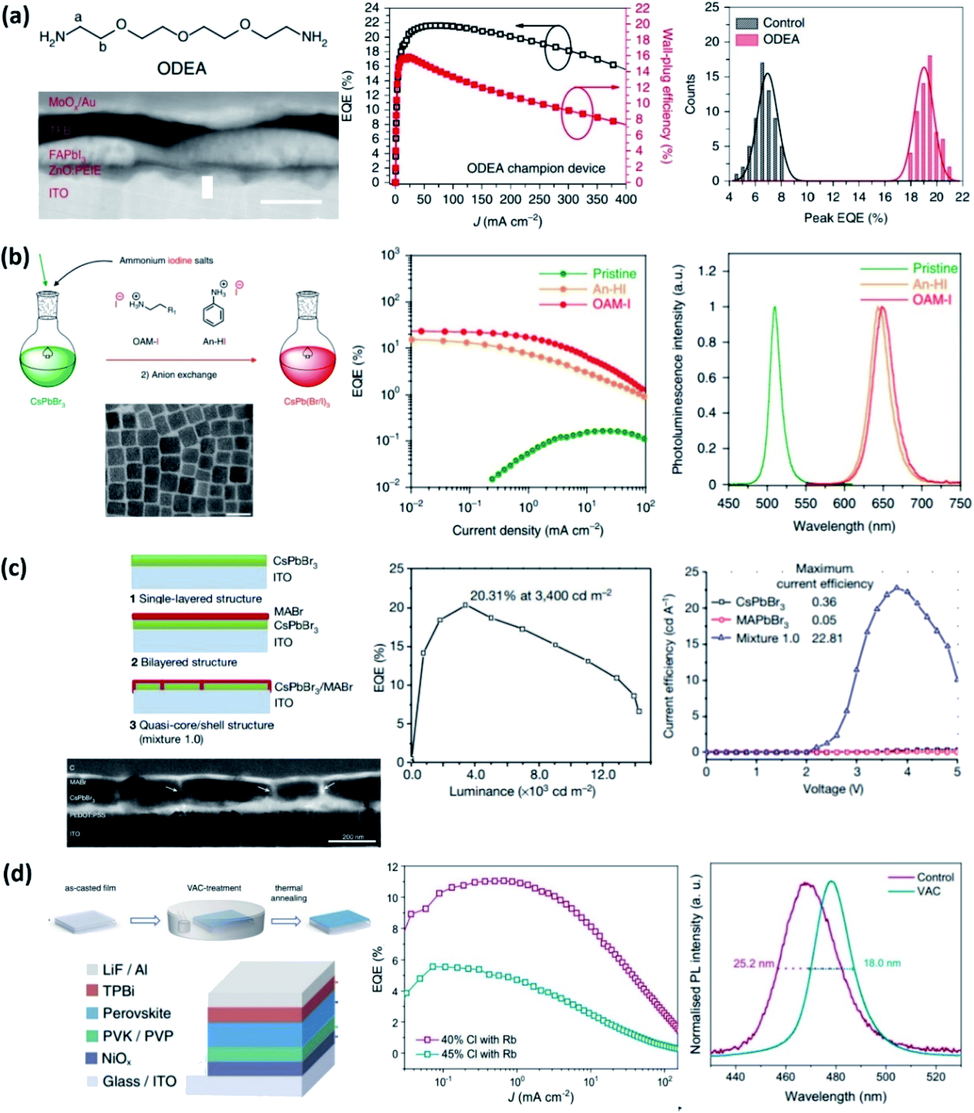 | ||
| Fig. 2 Latest advances with record efficiencies for near infrared, red, green and blue spectra. (a) Structure of 2,2′-[oxybis(ethylenoxy)]diethylamine (ODEA) and the SEM image of the device configuration with the corresponding values of EQE concerning the control sample. Reproduced with permission from ref. 53. Copyright 2019 Springer Nature. (b) Scheme of anion exchange of synthesized pristine CsPbBr3 perovskite QDs using long alkyl ammonium and aryl ammonium. The corresponding SEM images of the nanocrystal structure and the EQE values of the anion-exchanged NCs compared with the pristine formulation. Reproduced with permission from ref. 54. Copyright 2018 Springer Nature SharedIt (c) Schemes of single-layered CsPbBr3, bilayered CsPbBr3/MABr, and quasi-core/shell CsPbBr3/MABr structures. The corresponding SEM images and the EQE value of the enhanced structure. Reproduced with permission from ref. 55. Copyright 2018 Springer Nature SharedIt (d) Schematic illustration of the VAC-treatment, the PeLED structure and the corresponding EQE results compared with the control sample. Reproduced with permission from ref. 56, https://creativecommons.org/licenses/by/4.0/. | ||
In their work, the authors start from the premise that the widely used amino-functionalized passivation agents (–NH2; PAs), form strong hydrogen bonds with the organic cations of the perovskites, showing a modest passivation effect that restrains the improvement of the EQELED. Establishing a direct relationship between the nature of these hydrogen bonds and the final performance of the PeLED, a novel design of the organic passivation agent was developed. The target was to weaken the hydrogen bonds reducing the electro-donor character of the amino groups. By introducing one additional O atom to form 2,2′-[oxybis(ethylenoxy)]diethylamine (ODEA), they were able to increase the inductive effect, obtaining a peak EQE up to 21.6% and reaching a high radiance of 308 W sr−1 m−2 at 3.3 V. For the red spectra, Kido and co-workers obtained an excellent 21.3% of EQELED performing an anion exchange from pristine CsPbBr3 using two ammonium iodine salts: long alkyl-based oleyl ammonium iodide (OAM-I) and aryl-based aniline hydroiodide (An-HI) (Fig. 2b).54 In addition, they showed higher stability of the resulting An-HI PeLED than the control, demonstrating how essential it is to simultaneously control the chemical composition together with the surface ligands of anion-exchange perovskite QDs. An EQELED up to 20.3% for the green spectra was recently reported by Sargent and co-workers (Fig. 2c).55 They used MABr as an additive to fabricate a CsPbBr3/MABr quasi-core-shell structure. The key to this work lies in controlling the crystallization process of CsPbBr3/MABr due to their different solubilities, leading to sequential crystallization in a single-step method. They attribute the enhanced efficiency to the passivation of non-radiative pathways in CsPbBr3 thanks to the presence of MABr. To achieve blue emission, the straightforward pathway is the tuning of the bromide and chloride ratio in the perovskite composition. However, photoluminescence quenching and poor stability were identified as challenges for the development of high-efficiency blue emitters. A recent work by Feng Gao and co-workers shows an effective strategy to reduce halide segregation, improving the compositional homogeneity of the final material as well (Fig. 2d).56 A vapour-assisted crystallization (VAC) technique is presented as the key to demonstrating a spectrally stable blue PeLED with an EQE value of 11.0% with an emission peak at 477 nm and with a peak luminance of 2180 cd m−2. The authors ascribed the enhanced spectral stability to a reduction in the defect density, which was the main reason for ion hopping in the bulk material. The VAC treatment facilitated the Ostwald ripening crystal growth, providing larger grains at the cost of the smaller ones and increasing homogeneity. Despite the efforts made to achieve highly efficient and stable blue PeLEDs, there is still a long way to go towards white emission. In addition, there are other alternatives to develop white PeLED materials, such as dimensionality; using wider gap 1D or 2D-layered perovskites.57,58
![[thin space (1/6-em)]](https://www.rsc.org/images/entities/char_2009.gif) 000 and 100000 h, the PeLEDs thus far can be operated at best for 100–1000 h.61
000 and 100000 h, the PeLEDs thus far can be operated at best for 100–1000 h.61
Several approaches have been used to improve the PeLED stability: the use of inorganic CsPbX3 perovskite reduces the thermal degradation significantly caused otherwise by the organic cations.62 The layered perovskite structures containing PEA molecules have shown high stability over two weeks at 55% RH, retaining 77% of the original PCE, due to the hydrophobic character of PEA.63 The structure of quasi 2D perovskite is generally defined as A′2An−1BnX3n+1 (1 ≤ n ≤ ∞), where A′ refers to a large organic cation (monoammonium cations R-NH3+ and diammonium cations +H3N-R-NH3+). The use of quasi-2D perovskite/poly(ethylene oxide) (PEO) has demonstrated promising results regarding spectral stability, together with perovskite–polymer composite films, which improves stability under constant bias.64,65 Effects like photo brightening (and photodarkening) related with the enhancement in the luminescence efficiency under continuous illumination, highlight the importance of defect passivation to improve efficiency and stability.66
The robustness of the triple cation perovskite formulation was used by Nazeeruddin and co-workers to demonstrate stable PeLEDs in the near-infrared, green and blue spectra. Applying a constant current for 500 min at room temperature, cesium-containing perovskites maintain 38% of the initial luminance (Fig. 3a).62 They developed an inverted device structure using sputtered ZnO nanoparticles as an electron selective and injection layer. The stability tests were performed with green and blue PeLEDs under encapsulation, pointing out the importance of the material nature itself during operation conditions beyond the moisture and oxygen effects.
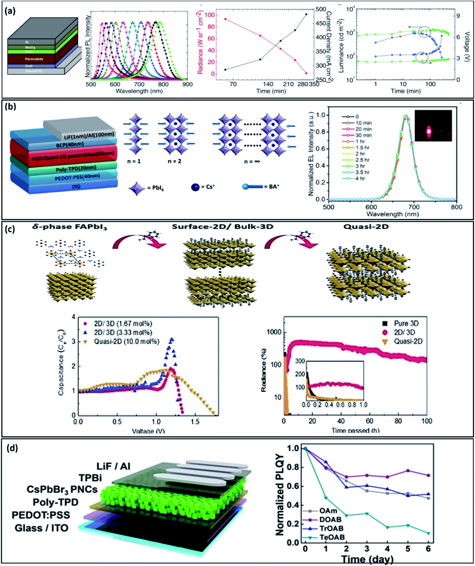 | ||
| Fig. 3 Remarkable advances obtained for high stability PeLEDs. (a) Perovskite light-emitting diode design, photoluminescence responses of different halide contents and the radiance and luminance recorded versus time. Reproduced with permission from ref. 62 Copyright 2017 WILEY-VCH Verlag GmbH & Co. KGaA, Weinheim (b) Device structure and the layered perovskite material based on PEO. Emission images of the different perovskite thicknesses showing the tuned colour and the normalized electroluminescence response versus time of the samples analysed. Reproduced with permission from ref. 64 Copyright 2018 WILEY-VCH Verlag GmbH & Co. KGaA, Weinheim. (c) Schematic illustration of the phase transition of 3D-FAPbI3 to the quasi-2D via the substitution of FA+ with aromatic ammonium cations (phenethyl ammonium, PEA+). The capacitance response versus voltage and the radiance versus time are also shown. Reproduced with permission from ref. 67 Copyright 2019 WILEY-VCH Verlag GmbH & Co. KGaA, Weinheim. (d) Device structure and the quaternary ammonium bromide derivatives analysed. PL emission of CsPbBr3 NC films under moisture conditions and the normalized XRD patterns of fresh CsPbBr3 NC films and the films after being kept in air. Reproduced with permission from ref. 69 Copyright 2019 American Chemical Society. | ||
An impressive electroluminescence stability of up to 4 hours at voltages as high as 3.5 V was reported by Ma and co-workers. Their red PeLEDs were based on the previously mentioned quasi-2D perovskite/poly(ethylene oxide) (PEO) (Fig. 3b).64 They used a cesium lead-based perovskite material, for its high stability properties, to prepare layered quantum well structures: (BA)2(Cs)n−1[PbnI3n+1] (BA: benzyl ammonium), with different thicknesses to tune the colour emission. The addition of PEO to the perovskite solution helped to form pinhole-free films with a smoother surface.
Related to the tuneable dimensionality of the perovskite bulk material, a recent work by Yang Yang and co-workers (Fig. 3c) shows an operational lifetime of T50: >200 h for a PeLED based on surface-2D/bulk-3D heterophase nanograins.67 They functionalized a pure α-FAPbI3 phase with a thin layer of surface-2D A2BX4/bulk-3D ABX3 hetero-phase substituting FA+ with aromatic ammonium cations (phenethyl ammonium, PEA+). The authors attribute the enhanced stability to surface-2D functionalization which leads to reduced monomolecular recombination, suppressing the α-FAPbI3 phase as well as lowering the ionic migration. In addition, they noticed a sharp decrease in the capacitance response which is related to a decrease in the charge accumulation at the interfaces. A lower charge density at the surface can reduce interfacial recombination processes improving as well the light emission.68
Surface ligand engineering of perovskite nanocrystals was addressed recently by Song and co-workers (Fig. 3d). Surface ligands affect charge-carrier confinement which leads to a high photoluminescence quantum yield. Their work systematically studied the effect of the carbon chain length concluding that the shorter the chain, the better the performance and stability of the PeLED. They replace the usual oleyamine with quaternary ammonium bromide (QAB), achieving an EQE of 9.7% introducing didecyldimethyl ammonium bromide ligands allowing a green emission for 6 days under moisture conditions.69
2.2. Lasers
A laser diode generates coherent radiation of high brightness. In contrast to light-emitting diodes which are based on spontaneous emission, lasers operate based on stimulated emission.70 During this process an incoming photon interacts with an excited electron which returns to a lower energy level by emission of another photon. Light amplification by stimulated emission requires population inversion, and thus in semiconductors, the quasi-Fermi splitting is larger than the bandgap energy.71 A laser is characterized by (i) a narrow linewidth emission, (ii) a clear threshold in both output power and linewidth versus pump power and (iii) a small divergence of the laser beam. A laser setup consists of an optical resonator (cavity) a pumping system and a laser gain medium for amplification of the radiation. The pumping system, which can be either optical or electrical, is needed for excitation to achieve the condition of population inversion. The laser-active gain determines the spectral bandwidth but also the threshold and saturation characteristics of the device.72 Some of the common materials used as gain media in laser diodes are gallium arsenide (GaAs) and indium gallium phosphide (InGaP). Perovskite materials, that can also be electrically pumped,73 could offer additional advantages such as low-cost, higher carrier mobilities, laser emission in the green/yellow wavelength region and reduced Joule heating when compared to other solution-processed materials.74,75In the following subsections, the perovskite composition and structural engineering for lasing applications are described via the latest advances to date to obtain a well-designed optical cavity, low lasing threshold and high output of the emitted photon flux to carriers injected.
A tuneable laser usually operates in a continuous mode with a small emission bandwidth. Several types of lasers can offer a wide wavelength tuning range. Solid-state bulk, dye, free-electron, quantum cascade and laser diodes, are just some of them.76–78 Laser diodes can be tuned to just a few nanometres, except for the so-called external-cavity diode laser that can be tuned to around 40 nm.79 Zhang and co-workers recently reported a strategy for tuneable perovskite lasers based on a solid–solid anion-diffusion process to construct a single CsPbClxBr3−x perovskite alloy nanowire (Fig. 4a).80 With this process they achieved a broad PL emission from 440 to 515 nm along the length of the nanowire due to the spatially graded halide distribution. They also demonstrated that the different spots along the nanowire can act as an optical cavity and as a gain medium at the same time.
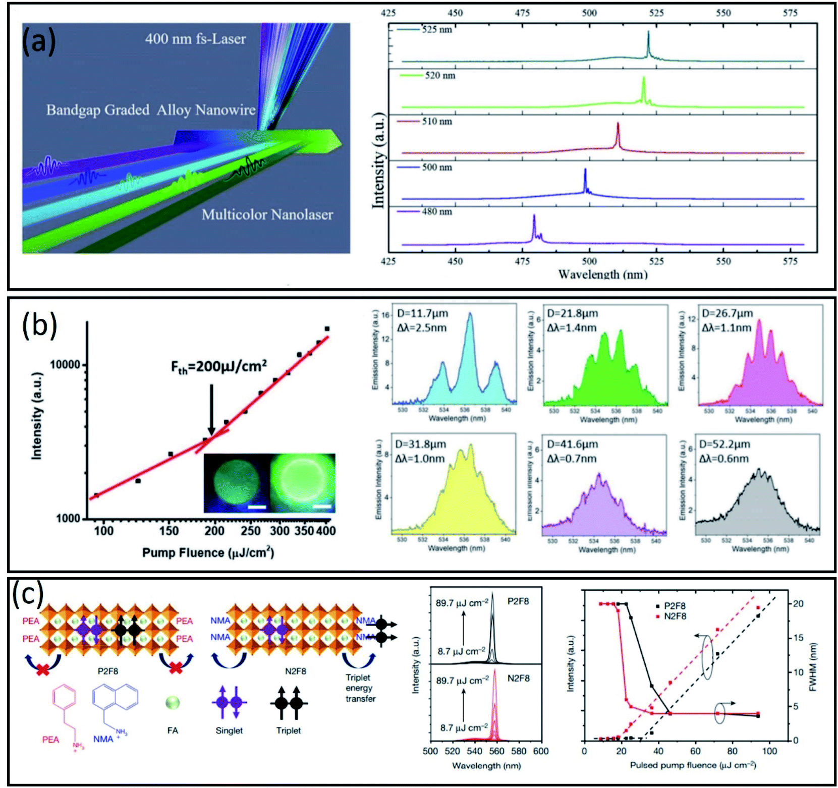 | ||
| Fig. 4 (a) Schematic representation of optical pumping lasing experiments with a 400 nm fs-laser (∼40 fs, 10 kHz) as the excitation source. Typical lasing spectra obtained from a single CsPbCl3−3xBr3x alloy nanowire at a high pump density. Reproduced with permission from ref. 80, Copyright 2020 The Royal Society of Chemistry. (b) Emission intensity versus excitation fluence measured from a CsPbBr3 QD microdisk and lasing spectra of QD microdisks with D = 11.7, 21.8, 26.7, 31.8, 41.6, and 52.2 μm, respectively. Δλ is the average “mode spacing” of the observed longitudinal cavity modes. Reproduced with permission from ref. 83, Copyright 2018 WILEY-VCH Verlag GmbH & Co. KGaA, Weinheim. (c) Chemical structures and evolution of emission spectra under pulsed excitation (3 ns) with different pump fluences. Photoluminescence, ASE and FWHM as a function of the pump fluence for a CW perovskite laser. Reproduced with permission from ref. 87, Copyright Springer Nature SharedIt. | ||
Multicolour or multi-wavelength lasers are the ones able to cover the broadband spectra. They are quite useful for white light generation, and are being applied in biological sensing and optical communication.81 CdSe/Cd1−xZnxSe1−ySy QDs have previously shown a reduced Auger decay of carriers, achieving a dual-colour lasing by optical pumping.82 Tsukruk and co-workers took advantage of this knowledge, making a perovskite multicolour laser through quantum dot (QD) patterning (Fig. 4b).83 The multicolour emission is achieved by initially fabricating a pattern of circular structures of green CsPbBr3 QDs and secondly, forming a complimentary pattern from a red-emitting material as CdSe/Cd1−xZnxSe1−ySy QDs.
A continuous-wave operation of a laser implies that it is continuously pumped, not pulsed, with consequent continuous light emission. The output power, in this case, could be approximately constant, but it can also present variations, that usually are resolved by introducing additional optical elements in the laser resonator.84 Quasi-2D perovskites containing larger secondary cations have demonstrated higher exciton binding energy and better stability than 3D perovskites.85 A stable optically pumped room-temperature continuous-wave (CW) laser based on quasi-2D perovskite films, was reported recently by Adachi and co-workers.86 In their work, they addressed the problem of the abrupt termination of lasing under CW optical pumping. They first consider the main issue during the CW working process for organic semiconductor gain media. This issue arises from the loss attributed to triplet accumulation and the consequent impossibility to stimulate the emission again.87 They observed the same detrimental process in quasi 2D perovskites, concluding that the single-triplet exciton annihilation could be directly related to the abrupt termination of the laser. Secondly, they applied triplet management strategies, using a distributed-feedback cavity with a high-quality factor, to obtain a CW green laser stable under room conditions (Fig. 4c).
A single-mode laser operates in longitudinal (axial) resonator mode or just in one single axial mode. In the case of a real single axial mode, the laser is considered to be a single-frequency laser in which the linewidth is very small, leading to a narrow optical emission spectrum.88 Zhang and co-workers recently reported a broad-band single-mode perovskite QD optically pumped laser (Fig. 5a).89 They made colloidal quantum dots (CQDs) based on CsPbX3 on a high-quality zinc oxide microrod hexagonal whispering-gallery microcavity. With this strategy, they obtained an ultra-narrow linewidth laser around 0.21 nm at 636 nm, with a quality factor of 3000. In addition, just tuning the halogen ratio, temperature and the size of the zinc oxide microrods, single-mode lasers were achieved across the entire visible spectrum.
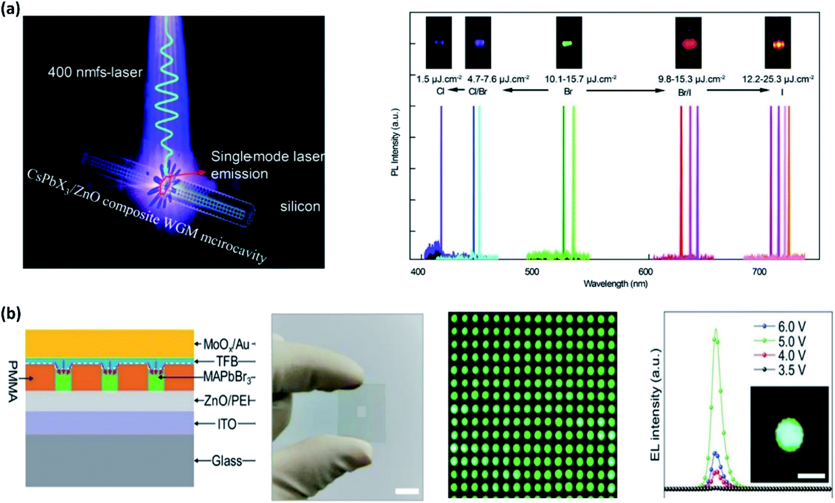 | ||
| Fig. 5 (a) Single-mode perovskite laser operating in a longitudinal resonator mode and the PL responses at different wavelengths. Reproduced with permission from ref. 89, Copyright 2020 The Royal Society of Chemistry. (b) Patterned surface with perovskite microdisk on top. Real images of the device and its emission with its corresponding PL response. Reproduced with permission from ref. 90. Copyright 2020 Wiley-VCH GmbH, Weinheim. | ||
Microarrays or microcavities act as resonators for light, possessing strong diffraction effects. One of the latest advances in perovskite microarrays was reported by Zhao and co-workers (Fig. 5b). They fabricated large-scale multicolor perovskite microdisk arrays through screen-printing.90 The dimensions and spatial locations of the microdisk were controlled via a predefined surface-energy pattern-assisted method in which electron-beam lithography acts as a screen-printing template. In addition, they were able to develop a multicolor optically pumped laser modifying the halide content, and lasing at a low threshold of 16.2 μJ cm−2.
3. Perovskites for sensing application
Sensors should meet some quality criteria such as high sensitivity, rapid response/recovery time and low electrical or optical signal hysteresis.91 So far, various semiconductors, including metal oxides, graphene composites, photonic crystals, and polymer materials, have been used for this purpose. However, so far, their application has been limited due to their complicated synthesis procedures, a narrow working range, and low sensitivity. The ease of processing, excellent optoelectronic properties, and high sensitivity to various gases or elements convert perovskite materials to the ideal candidate for different sensor applications. Various sensing abilities of perovskite materials will be discussed in the following parts.3.1 Humidity sensors
Humidity sensing devices emerged as an essential technology for various applications such as health monitoring, food safety, hospital apparatus, agricultural fields and forecasting climate change.92,93 Generally, besides the high sensitivity and response/recovery time, a humidity sensor should retain long-term stability and reliability with reversible behavior, even in high-humidity environments.Ceramic-based humidity sensors have been developed over several decades.94 Despite their numerous advantages, such as high sensitivity, and high physical and chemical stability, they face many challenges such as poor linearity over a wide humidity range and chemisorption of water molecules, which confines their application.95
As mentioned, perovskite materials have shown great potential to sense the humidity in different ranges. The organic and inorganic portions are held together by ionic and hydrogen-bonding interactions between the NH3+ cations and the halides atoms in the perovskite structure.96 In humid environments, the water molecules can penetrate the perovskite lattice and occupy a similar space to cations, i.e. MA+, by forming strong hydrogen bonds with halides, changing the optoelectronic and morphological properties (Fig. 6a).97,98 Therefore, investigating the interaction between water molecules and the crystal lattice is necessary to understand the perovskite sensing properties. Moreover, the key critical point before using perovskite materials as a humidity sensor could be finding a proper sensitivity characterization method. So far, the humidity sensing properties of perovskite materials have been characterized by measuring their resistance, capacitance and photoluminescence properties under humid conditions.91
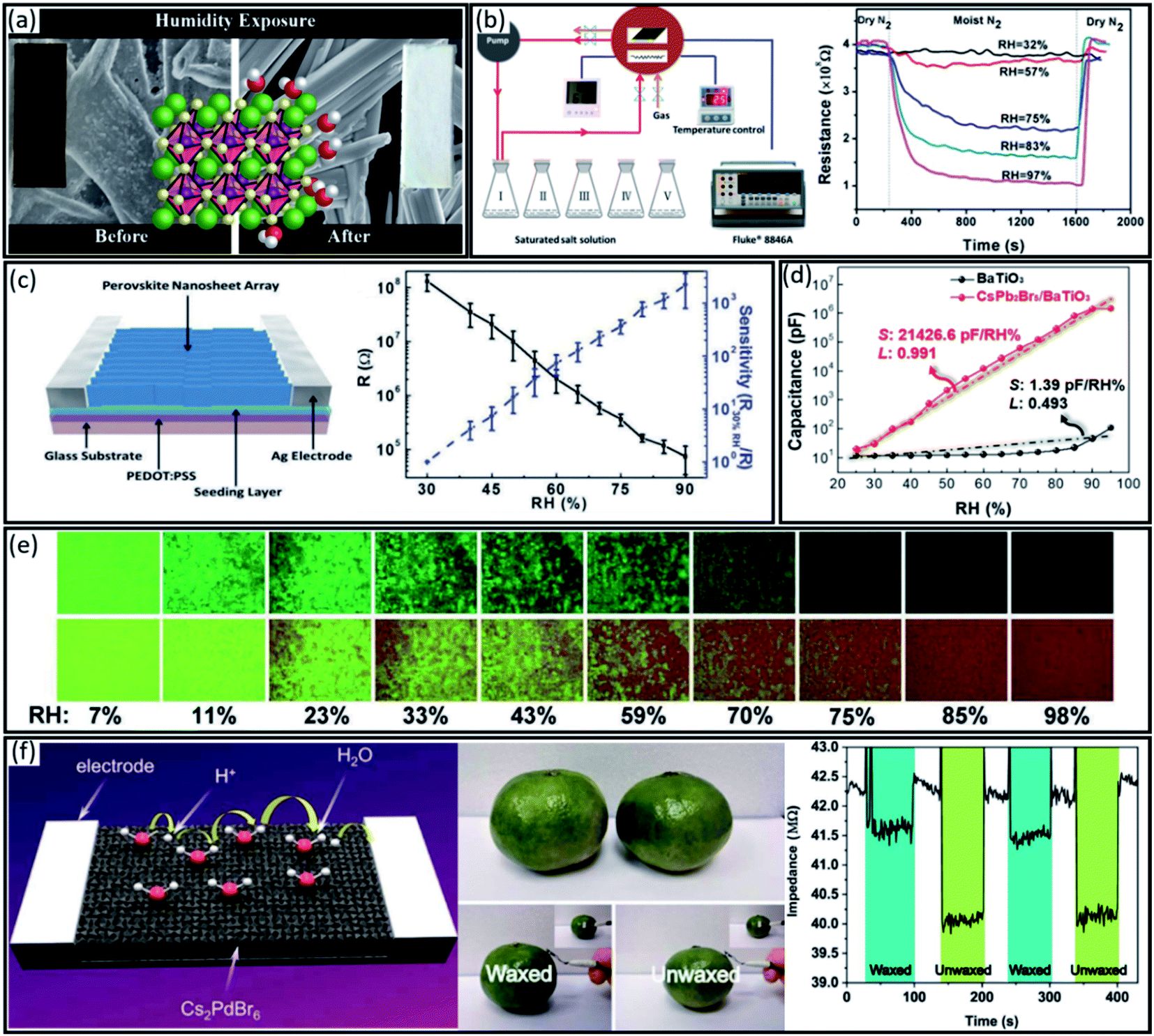 | ||
| Fig. 6 (a) SEM, photograph and crystal structure of MAPbI3 perovskite before and after humidity exposure. Reproduced with permission from ref. 98, Copyright 2015 American Chemical Society. (b) Schematic of the resistance measurement set-up and the resistance curves at various moisture levels at room temperature. Reproduced with permission from ref. 99, Copyright 2015 American Chemical Society. (c) Schematic illustration of the sensor structure, the average resistance (black line) and the resistance response sensitivity (blue line) under various RH conditions. Reproduced with permission from ref. 100, Copyright 2017 the Royal Society of Chemistry. (d) The humidity detection performance of CsPb2Br5/BaTiO3 and BaTiO3 sensors (capacitance vs. RH; S: sensitivity; L: linearity). Reproduced with permission from ref. 101, Copyright 2020 John Wiley and Sons. (e) Colour responses of the humidity sensor in various humidity ranges (7 to 98%) at room temperature. Reproduced with permission from ref. 102, Copyright 2016 the Royal Society of Chemistry. (f) Schematic illustration of the humidity sensing mechanism of the Cs2PdBr6 sensor, photographs of waxed and unwaxed oranges, and dynamic responses of the waxing detector to waxed and unwaxed oranges at 29 °C and 48 RH%. Reproduced with permission from ref. 111, Copyright 2020 the Royal Society of Chemistry. | ||
For example, Liu et al.99 designed an in situ electrical resistance measurement to record the interaction between moisture and CH3NH3PbI3−xClx perovskites film under controllable conditions (Fig. 6b). They recorded the resistance during the exposure of a perovskite film to a moist N2 flow. As shown in Fig. 6b, by increasing the humidity level from 32% to 97%, the resistance decreased from 98% to 25% of the initial value. Interestingly, the resistance of the perovskite film was fully recovered to the initial value within 74 s after exposure to a severe humidity of 97% for 10 min, indicating the fully reversible chemisorption and hydration of the perovskite film in the short term. However, extending the exposure time led to irrecoverable resistance due to the transformation of the chemisorption to chemical reaction and decomposition of perovskite into PbI2.
Besides, increasing the surface area of active materials in sensors can increase their sensitivity. Therefore, Ren et al.100 designed highly uniform nanosheet perovskite arrays to increase the sensitivity and responsivity to water molecules (Fig. 6c). They found that a chlorine-based perovskite structure, i.e. CH3NH3Pbl3xCIx, is more beneficial for sensor performance due to lower decomposition in a humid environment. As shown in Fig. 6c, similar to the report by Liu et al.99, the resistance sharply dropped from 1.28 × 10⁸ to 7.39 × 10⁴ Ω by increasing the moisture from 30% to 90%, indicating strong sensitivity of the perovskite arrays. Moreover, this perovskite sensor presented a negligible resistance hysteresis during the reverse and forward humidity monitoring, confirming excellent device reversibility (Fig. 6c).
Besides resistive-type humidity sensors, capacitive-type ones have shown better relative humidity sensing performance. However, as mentioned, ceramic capacitive-type humidity sensors face some challenges regarding poor linearity and sensitivity over a wide humidity range. To answer this challenge, Cho et al.101 developed a new capacitive-type humidity sensor by combining the perovskite material, i.e. CsPbBr3 or CsPb2Br5, with diverse metal oxides, i.e. Al2O3, TiO2, and BaTiO3. The nanocomposite powder was deposited on substrates utilizing the aerosol deposition (AD) method. As shown in Fig. 6d the CsPb2Br5/BaTiO3 nanocomposite exhibited a high humidity sensitivity of 21426 pF per RH% with a superior linearity of 0.991 and excellent stability in a wide range of relative humidity compared to CsPbBr3/Al2O3 and CsPbBr3/TiO2 sensors with a sensitivity of 1.75 and 2005.17 pF per RH%, respectively. The highly porous structure, effective charge separation, and water-resistant characteristics of CsPb2Br5 perovskite were demonstrated as the main reasons for the high sensitivity and stability of this sensor.
In addition to resistivity and capacitance properties, perovskite materials exhibit very interesting fluorescence properties sensitive to the wide range of humidity. First, W. Xu et al.102 demonstrated a linearly inverse relation between the fluorescence intensity of MAPbBr3 perovskite and relative humidity (RH). As shown in Fig. 6e, humidity sensing was realized with the naked eye with an ideal resolution of apparent colour in the RH range from 7 to 98%. Interestingly, the fluorescence intensity showed reversible behaviour by decreasing the humidity amount, which is reasonably necessary for an ideal humidity sensor.
However, the toxicity and environmental instability of lead-based perovskite materials hinder their application as a sensor, which needs to be addressed before commercialization. Substitution of Pb2+ central metal by a trivalent metallic element (B′ = Sb3+ and Bi3+) and a monovalent metallic element (B′′ = Cu+, Ag+, and Au+) with a general formula of A2B′B′′X6 has been highlighted as an interesting approach to design lead-free and stable perovskites. However, the B-site cation in A2B′B′′X6 could be replaced with a vacancy, which leads to a vacancy-ordered defect variant perovskite with the A2BX6 formula. For example, Sn and Te have been used as B cations in the A2BX6 structure to provide a less-toxic and chemically stable perovskite for light-absorbing application from the visible to infrared (IR) regions.103,104 Besides, other lead-free perovskites such as Cs2AgBiBr6, Cs2BiAgCl6, Cs2SnI6, Cs2TeI6, Cs2TeCl6, Cs2TiBr6 and Cs2PdBr6 have been synthesized successfully.29,103,105–109 However, besides being lead-free with reasonable stability, these materials should have proper optoelectronic properties for sensor application. Interestingly, lead-free perovskite Cs2PdBr6 with an optical band gap of 1.6 eV and long-lived photoluminescence showed a high moisture resistance.110 This new semiconductor material could be prepared by in situ oxidation of Pd2+ to Pd4+ during the solution process synthesis. As a result, cubic Cs2PdBr6 crystals with space group Fm![[3 with combining macron]](https://www.rsc.org/images/entities/char_0033_0304.gif) m was synthesized. Very recently, W. Ye et al. demonstrated the high humidity sensing properties of the Cs2PdBr6 thin film.111 They further improved the moisture stability of Cs2PdBr6 by oleic acid (OA) passivation, increasing the surface hydrophobicity. Therefore, passivated Cs2PdBr6 showed lower water molecule absorption and higher desorption than the non-passivated sample, resulting in a longer response time and shorter recovery time. Regarding the humidity sensing mechanism, first, under an external electric field, the absorbed water molecules dissociate into free protons and form H3O+ ions. Secondly, due to the good carrier mobility of Cs2PdBr6, after a certain adsorption amount of water molecules, i.e. high humidity conditions, H3O+ ions start to migrate inside and outside the perovskite, resulting in a gradually decreasing resistivity (Fig. 6f). Due to the high humidity sensitivity and fast response/recovery, the Cs2PdBr6-based sensor was used for fruit waxing detection. As shown in Fig. 6f, the pen-like Cs2PdBr6 detector was placed close to the waxed and unwaxed oranges, which have been already treated in constant humidity (48 RH%) for 12 h. The unwaxed orange showed a lower impedance signal than the waxed orange, confirming higher humidity due to the uncovered surface (Fig. 6f).
m was synthesized. Very recently, W. Ye et al. demonstrated the high humidity sensing properties of the Cs2PdBr6 thin film.111 They further improved the moisture stability of Cs2PdBr6 by oleic acid (OA) passivation, increasing the surface hydrophobicity. Therefore, passivated Cs2PdBr6 showed lower water molecule absorption and higher desorption than the non-passivated sample, resulting in a longer response time and shorter recovery time. Regarding the humidity sensing mechanism, first, under an external electric field, the absorbed water molecules dissociate into free protons and form H3O+ ions. Secondly, due to the good carrier mobility of Cs2PdBr6, after a certain adsorption amount of water molecules, i.e. high humidity conditions, H3O+ ions start to migrate inside and outside the perovskite, resulting in a gradually decreasing resistivity (Fig. 6f). Due to the high humidity sensitivity and fast response/recovery, the Cs2PdBr6-based sensor was used for fruit waxing detection. As shown in Fig. 6f, the pen-like Cs2PdBr6 detector was placed close to the waxed and unwaxed oranges, which have been already treated in constant humidity (48 RH%) for 12 h. The unwaxed orange showed a lower impedance signal than the waxed orange, confirming higher humidity due to the uncovered surface (Fig. 6f).
3.2. Temperature sensors
Temperature sensors are widely used in all heating and cooling based devices for temperature monitoring in daily life, industry and medical applications.112,113 Temperature sensors have great potential and represent about 75–80% of the global sensor market.114In addition to the traditional liquid-filled glass thermometers, thermocouples are the most frequent traditional temperature sensors. However, besides environmental and health concerns about these kinds of sensors, they do not have enough resolution in the spatial range of <10 μm, which is necessary for temperature monitoring in microfluidic systems or inside living cells. Optical temperature sensors have emerged as an excellent technology for contactless measurement and large-scale imaging to respond to this challenge.115
Indeed, infrared (IR) thermometers have been the first optical-based temperature sensors.116 However, this type of optical sensor faces a lack of good spatial resolution and depends on the target materials. As a substitute, luminescence-based materials, including fluorescence and phosphorescence, have recently attracted attention.117 This type of thermometry is highly dependent on the electronic band structure of the active material. As shown in Fig. 7a, thermal energy excites the electrons within the excited states, leading to temperature-dependent luminescence emission. Since the perovskite crystal phase can change at different temperatures the material also changes its optical and electronic properties. For example, all-inorganic CsPbBr3 perovskite shows an orthorhombic phase, i.e. a yellow phase, at room temperature, while by heating up to 403 K the phase can be transformed into a photoactive cubic structure, i.e. a black phase (Fig. 7b). As a result, the temperature-dependent phase transformation of perovskite materials can be evaluated by tracing their photoluminescence (PL) characteristics, including peak intensity and wideness, and PL lifetime. This property of perovskite materials can be beneficial for fluorescent temperature sensor application as first demonstrated by Y. Niu et al.118 They illustrated that perovskite materials with both high luminance sensitivity (1.3% K−1) and good reversibility (>500 cycles) over a wide temperature range of 0–80 °C may be an ideal temperature sensor. The 2D (CnH2n+1NH3)2PbI4 perovskite exhibits reversible phase transition, presenting a temperature-dependent luminescence. As a systematic study, thin film temperature sensors were fabricated by dipping a piece of filter paper into hexane solutions of (CnH2n+1NH3)2PbI4 (n = 4, 12, 16, and 18) perovskites. Fig. 7c shows the temperature-dependent PL spectra for the optimized sensor, i.e. (C16H33NH3)2PbI4, in which the peak intensity decreased by increasing the temperature linearly. However, the peak position is slightly redshifted to a longer wavelength by increasing the temperature following the inverse temperature dependence of the bandgap. This temperature sensor was also successfully applied in thermal imaging. As shown in Fig. 7d, the heated (C16H33NH3)2PbI4 film indicates/images the temperature distribution due to a quenched PL intensity for different temperatures with high spatial distribution, which was confirmed by using a thermal infrared imager.
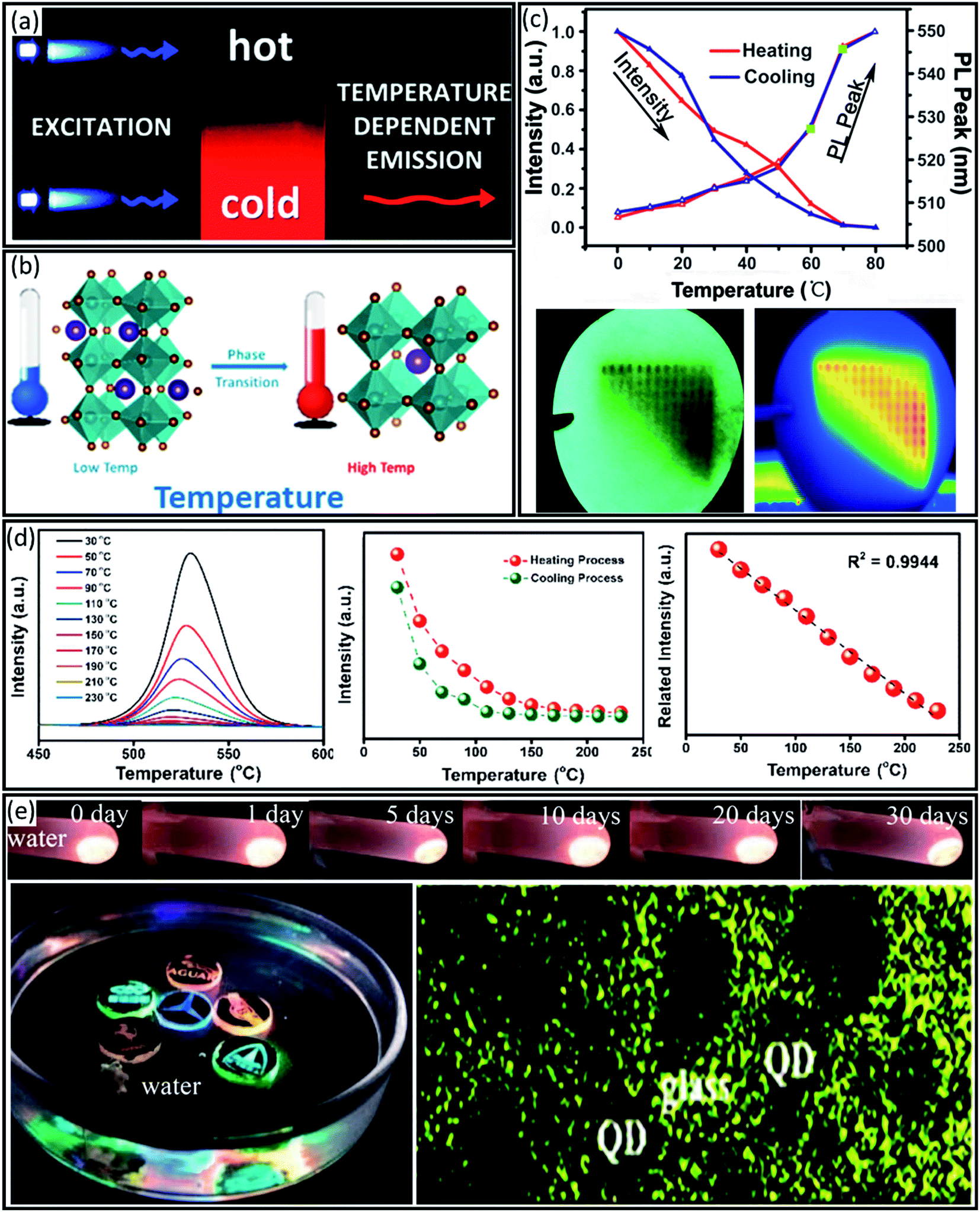 | ||
| Fig. 7 (a) Schematic illustration of temperature-dependent luminescence emission. Reproduced with permission from ref. 112, Copyright 2013 the Royal Society of Chemistry. (b) Schematic illustration of a perovskite phase transition by applying temperature. Reproduced with permission from ref. 91, Copyright 2018 the Royal Society of Chemistry. (c) PL intensity and peak position in different temperatures during heating and cooling. The bottom panel shows a comparison of the PL intensity map of the sensor film (left) and an infrared image (right) when applied to a hotplate. Reproduced with permission from ref. 118 Copyright 2014 John Wiley and Sons. (d) PL spectra of CH3NH3PbBr3@MOF-5 composites for different temperatures from 30 to 230 °C, the fluorescence emission intensities under heating and cooling temperatures and the linear fitting of the emission intensity variation. Reproduced with permission from ref. 119, Copyright 2018 American Chemical Society. (e) Luminescence photographs of Mn-doped CsPbCl3 PQDs@glass immersed in water for different storage times, the carving auto patterns of nanocomposites in water, and TEM images of embedded CsPbCl3 PQDs in a glass matrix. Reproduced with permission from ref. 121, Copyright 2019 the Royal Society of Chemistry. | ||
Yet, other perovskite compositions such as MAPbBr3 nanocrystals (NCs) showed great potential for temperature sensing application, too. For example, D. Zhang et al.119 employed highly stable encapsulated MAPbBr3 NCs with an MOF-5 composite, i.e. MAPbBr3@MOF-5. The PL intensity decreased steadily when increasing the temperature from 30 °C to 230 °C with a high recovery rate of 96.4% of the initial PL intensity after cooling down to 30 °C. Notably, MAPbBr3 itself can decompose at temperatures above 180 °C, while MAPbBr3@MOF-5 NCs showed an excellent linear relationship with a correlation coefficient (R2) of 0.9944, enabling its application as a luminescent thermometer within the tested temperature range (Fig. 7d).
However, some of the volatile components in organic–inorganic perovskites such as MA+ or FA+, in MAI or FAI forms may degas at temperatures as low as 100 °C and create cation vacancies in the perovskite structure leading to a decreased thermal stability.119 To address this challenge, all-inorganic perovskites such as CsPbI3, CsPbIxBr1−x, and CsPbBr3 with thermal stability over 400 °C have been introduced. This could potentially be used for temperature sensing.120 By embedding dual-emitting Mn-doped CsPb(Cl/Br)3 NCs in a glass matrix, B. Zhuang et al.121 developed an ultra-stable ratio metric temperature sensor which showed a linear temperature-dependence of the PL peak ratio (PR) between the exciton and Mn2+ emission in the range of 80–293 K. As shown in Fig. 7e, the luminescence intensity was retained in water over 30 days. Interestingly, the carving patterns of car logos designed using different nanocomposites with a wide emission range were stable for a long time in water (Fig. 7e). Moreover, they also confirmed that the protective inorganic oxide glass could completely inhibit unfavourable halogen anion exchange for different perovskite compositions (Fig. 7e).
3.3. Gas sensors
Gas sensors or gas detectors are commonly used to identify different types of gases, having a wide range of applications such as air quality monitoring and detecting toxic or explosive gasses.122 Developing new materials with high sensitivity and selectivity with fast response and long-term stability have been assigned as an exciting research direction in the gas sensor field. Particularly, an ideal gas sensor should be operated at room temperature. However, most traditional gas sensors are fabricated from semiconducting oxide-based materials, which can work only at high temperatures.123,124 Perovskites are of particular interest for the development of gas sensors thanks to their super-sensitive structure and excellent optical and electrical properties. Zhao et al.125 revealed that MAPbI3 can absorb and desorb NH3 molecules at different concentrations. Later, Bao et al.126 developed an NH3 gas sensing set-up based on a MAPbI3 perovskite film (See Fig. 8a). They demonstrated that the film resistance significantly decreased upon exposure to an NH3 atmosphere at room temperature and recovered to its initial value within seconds after disconnecting the NH3 atmosphere. As shown in Fig. 8a, when turning on the NH3 supply, the current increased from 10 nA to a saturation current of 110 nA in 3 s. When stopping the NH3 flow, the current recovered to below 10 nA in only 4.5 s. Due to its very short response time the perovskite-based sensor is well suitable for NH3 sensing applications.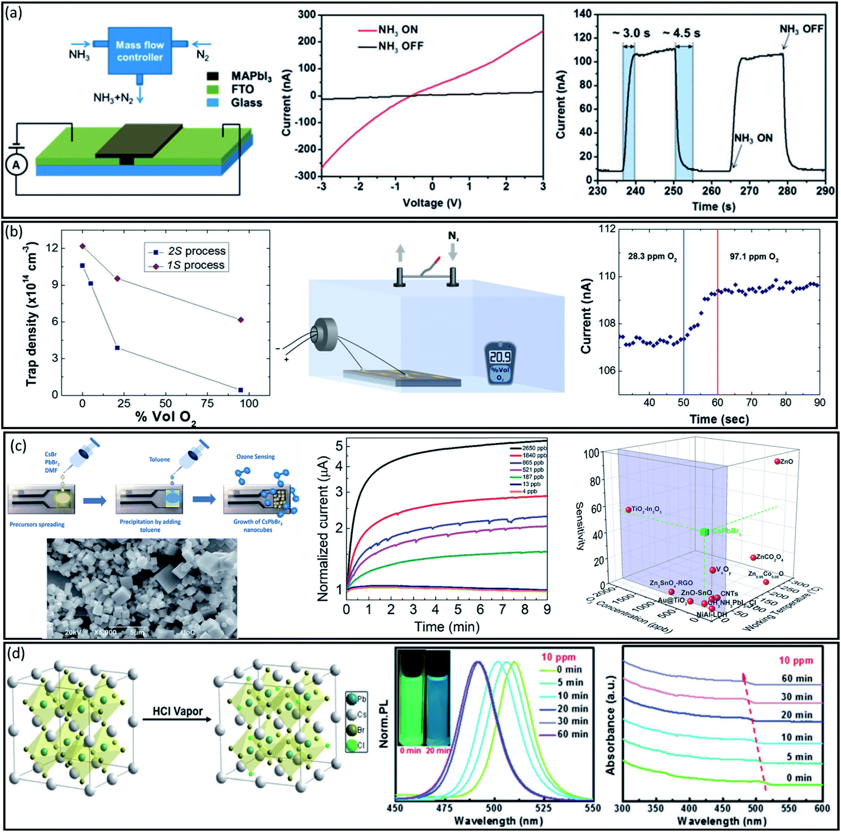 | ||
| Fig. 8 (a) Schematic illustration of the resistance measurement set-up for NH3 gas sensing of an MAPbI3 film, the I–V curves and enlarged view of I–t curves during NH3 ON and OFF at room temperature. Reproduced with permission from ref. 126, Copyright 2015 the Royal Society of Chemistry. (b) The number of charge traps for 1S and 2S perovskite films at different oxygen concentrations, the schematic of the experimental setup for O2 sensing characterization and the real-time current change corresponding to a 70 ppm O2 variation in the sample atmosphere. Reproduced with permission from Ref.127, Copyright 2014 John Wiley and Sons. (c) Schematic illustration of ozone sensor fabrication and the SEM image of CsPbBr3 nanocubes, the electrical response of the CsPbBr3 sensor upon applying various ozone concentrations and ozone sensitivity of a CsPbBr3 sensor compared to other types of sensors. Reproduced with permission from ref. 129, Copyright 2019 the Royal Society of Chemistry. (d) Schematic of the anion-exchange reaction between gaseous HCl and CsPbBr3 perovskite, the PL spectra of exposed CsPbBr3 nanocrystals to HCl for different times (insets show the photograph of the visual changed colour of sample exposed to 10 ppm HCl for 20 minutes) and the UV-vis absorption spectra of CsPbBr3 nanocrystals exposed to 10 ppm HCl for different times. Reproduced with permission from ref. 130, Copyright 2017 the Royal Society of Chemistry. | ||
Due to their low formation energy, cation or halide vacancies are usually present in the perovskite crystal. Stöckel et al.127 passivated the iodine vacancy defects on the MAPbI3 film surface using O2 molecules, applying them for O2 sensing. As shown in Fig. 8b, the trap densities of both one step (1S) and two step (2S) deposited films were decreased in the presence of O2 compared to those in the N2 atmosphere. Fig. 8b shows the designed oxygen sensor set-up by measuring the electrical properties of perovskite films at different O2 levels. They measured an O2 concentration as small as 70 ppm in a short time (<400 ms) on the surface of a perovskite film with a fully reversible behaviour (Fig. 8b). In another report, H. Chen128 used a porous CsPbBr3 network device with a VOC of 0.87 V under visible-light irradiation to detect various concentrations of O2. They demonstrated that illumination could noticeably improve response to O2 because of the pumping of charge carriers and desorption of unwanted surface species of a CsPbBr3 film. As a result, the fabricated oxygen sensor showed a relatively fast response time of 17.4 s with acceptable stability and reproducibility and a short recovery time of 127.9 s.
Regarding all-inorganic perovskite materials K. Brintakis et al.129 used CsPbBr3 perovskite for ozone sensing with a high sensitivity of 54% in 187 ppb and remarkable reproducibility compared to organic–inorganic perovskite, i.e. CH3NH3PbI3xClx. As shown in Fig. 8c, CsPbBr3 nanocubes with sizes ranging from 500 nm to 1 mm were directly formed on a pre-patterned electrode substrate through a fast and straightforward re-precipitation method at room temperature. In the electrical response of the sensor upon exposure to different concentrations of ozone gas from 2650 down to 4 ppb, ozone was detected within less than 1 min (Fig. 8c). Moreover, when compared to other semiconducting materials, this CsPbBr3 nanocube-based sensor was able to detect the lowest ozone concentrations under room temperature working conditions (Fig. 8c).
Since in many industrial processes, gaseous and aqueous hydrochloric acid (HCl) exhaust is a major problem, accurate detection of HCl is very critical for the industry. To tackle this challenge, Chen et al.130 used CsPbBr3 nanocrystals (NCs) to fabricate an optical gas sensor based on the anion-exchange reaction for HCl vapor sensing. As shown schematically in Fig. 8d, by exposing CsPbBr3 NCs to HCl gas through a facile gaseous anion exchange reaction, the gaseous Cl species partially substituted Br ions. The PL spectra of CsPbBr3 NCs exposed to HCl vapor with a concentration of 10 ppm showed a blue shift from 513 nm to 508, 502 and 495 nm after 5, 10 and 20 minutes, respectively (Fig. 8d). However, after 30 min the PL profiles were stabilized, indicating the established equilibrium of the gaseous anion-exchange reaction between Cl and Br ions under operational conditions. Consequently, CsPbBr3 NCs can be used as a highly sensitive and selective spectrochemical sensor for the detection of gaseous HCl.
3.4. Solvent sensors
Perovskite materials have shown great potential for solvent sensor applications due to their ionic nature and high sensitivity to solvents. For example, Niu et al.118 probed the fluorescence properties of (C16H33NH3)2PbI4 perovskite in different solvents. As shown in Fig. 9a, the perovskite powder was completely dissolved in THF, and a non-emissive transparent solution was formed. However, a yellow precipitate was produced by dissolving perovskite powder in water as a polar solvent. As schematically shown in Fig. 8a, the layered (C16H33NH3)2PbI4 perovskite structure was well separated in THF, while it aggregated into a layered quantum-well structure when water was introduced. As a result, the PL emission dramatically increased by over 70%.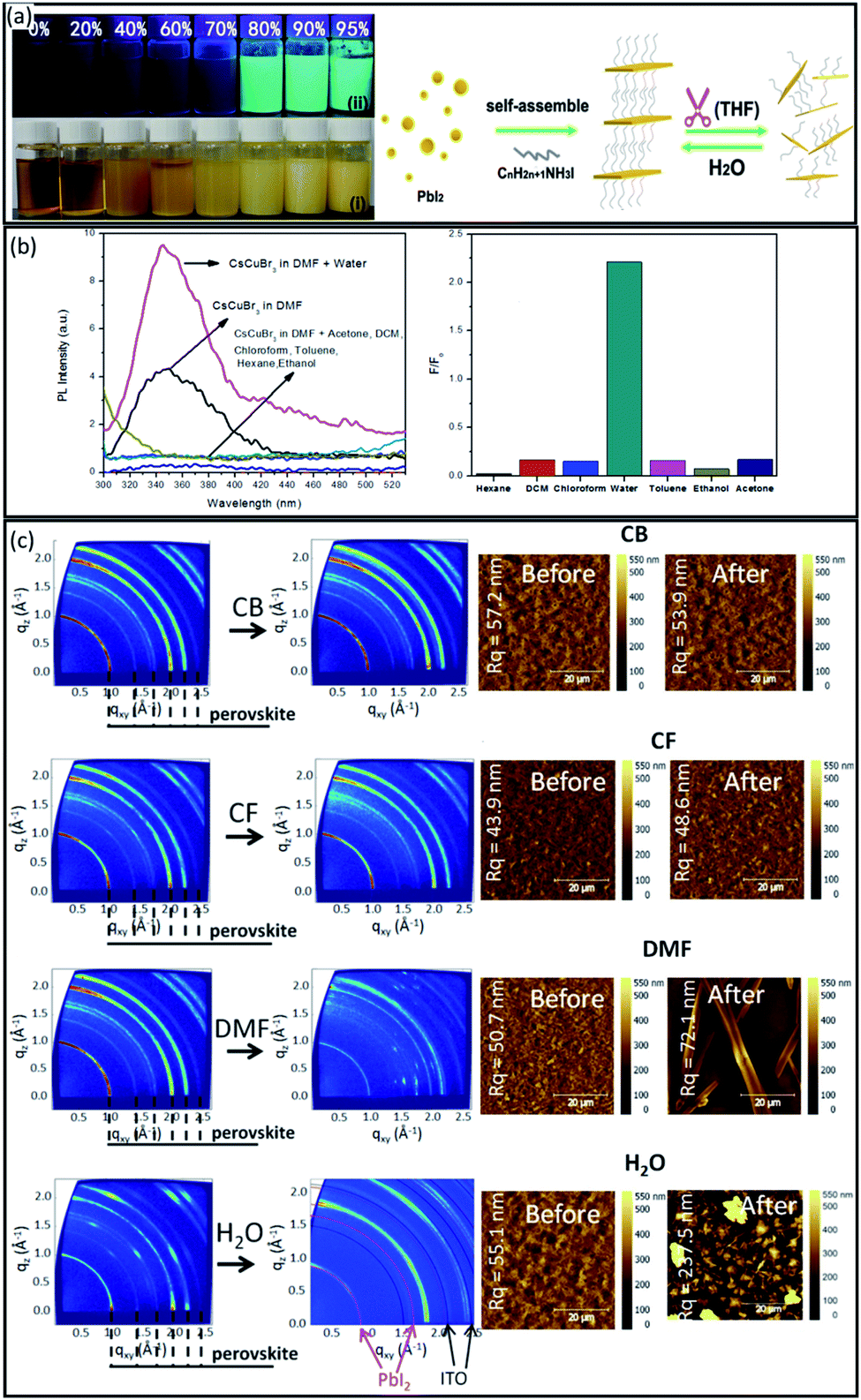 | ||
| Fig. 9 (a) Photographs of solution/suspensions of (C16H33NH3)2PbI4 with different water contents under ambient (i) light and (ii) UV-365 nm radiation, and schematic illustration of the solvent sensing mechanism of (C16H33NH3)2PbI4 perovskite. Reproduced with permission from ref. 118, Copyright 2014 John Wiley and Sons. (b) Photoluminescence spectrum and solvent selectivity of the perovskite compound in the presence of various solvents. Reproduced with permission from ref. 131 Copyright 2016 Elsevier. (c) 2D GIXRD patterns and AFM images of MAPbI3-xClx films before and after different solvent exposure. Reproduced with permission from ref. 132 Copyright 2019 Springer. | ||
Moreover, Aamir et al.131 successfully used cesium-based copper bromide inorganic perovskite (CsCuBr3) NCs as a sensor to detect water contamination in dimethylformamide (DMF). As shown in Fig. 9b, the addition of water to DMF increased the fluorescence intensity peak of CsCuBr3, possibly due to the better electron donation of water molecules compared to DMF. However, the PL intensity was decreased by adding other solvents such as dichloromethane, chloroform, toluene, hexane, ethanol and acetone to CsCuBr3 solution (Fig. 9b), indicating the specific selectivity of the perovskite sensor towards water molecules.
Recently, Ralaiarisoa et al.132 systematically investigated the impact of four prototypical solvents on the structural and electronic properties of MAPbI3−xClx perovskite films. Chlorobenzene (CB) and chloroform (CF) were chosen as a common solvent of charge transport materials for spiro-MeOTAD or PCBM, i.e. HTL or ETL, deposition, and dimethylformamide (DMF) and water (H2O) were selected as typical polar solvents for dissolving perovskite materials. Fig. 9c shows the 2D GIXRD patterns and corresponding AFM images of the MAPbI3−xClx perovskite films before and after respective solvent exposure. After CB and CF exposure, no noticeable change in the GIXRD patterns and film morphology was observed, indicating that CB and CF did not significantly affect the perovskite crystal structure. However, exposure to DMF and H2O lead to dramatic changes in the GIXRD patterns and morphology of perovskite films. When exposed to DMF, the perovskite film became transparent due to the dissolution of the solid film, and the GIXRD patterns still exhibit a perovskite peak at q = 1 Å−1 with a lower intensity than the original pattern, possibly due to the incomplete re-crystallization during the drying of the film in ambient air at room temperature. However, the perovskite film readily turned yellow when exposed to H2O, and the GIXRD pattern proved that the perovskite film immediately degraded into PbI2 without an intermediate phase such as lead monohydrate. These findings were further confirmed by the addition of optical and elemental characterization. In summary, it can be concluded that perovskite materials exhibit various behaviour for different solvents, which may be exploited for solvent sensing applications.
4. Further applications
Space applications, gamma-ray detection, thermochromic devices, data storage and colloidal systems are additional application areas for metal-halide perovskites.Yet, the longest lifetime reported for perovskite solar cells (PSCs) has so far been less than 2 years.25 The major concern is the material’s intrinsic instability upon exposure to moisture and oxygen. However, the idea of space application of this material gains importance especially since PSCs would operate in an environment without or extremely low levels of water and oxygen. In fact, recent studies have reported significant advantages regarding the light weight of PSCs and their surprising tolerance against high-energy particle irradiation.133,134 Zhu and co-workers investigated the stability of PSCs that were fixed on a balloon (see Fig. 10a) raised to an altitude of 35 km in near space. The mixed cation perovskite FA0.81MA0.10–Cs0.04PbI2.55Br0.40 solar cells retained 95% of the initial efficiency of 6.3%.135 Further tests with higher efficiency devices will be needed to evidence the great potential of perovskites for space solar cells.
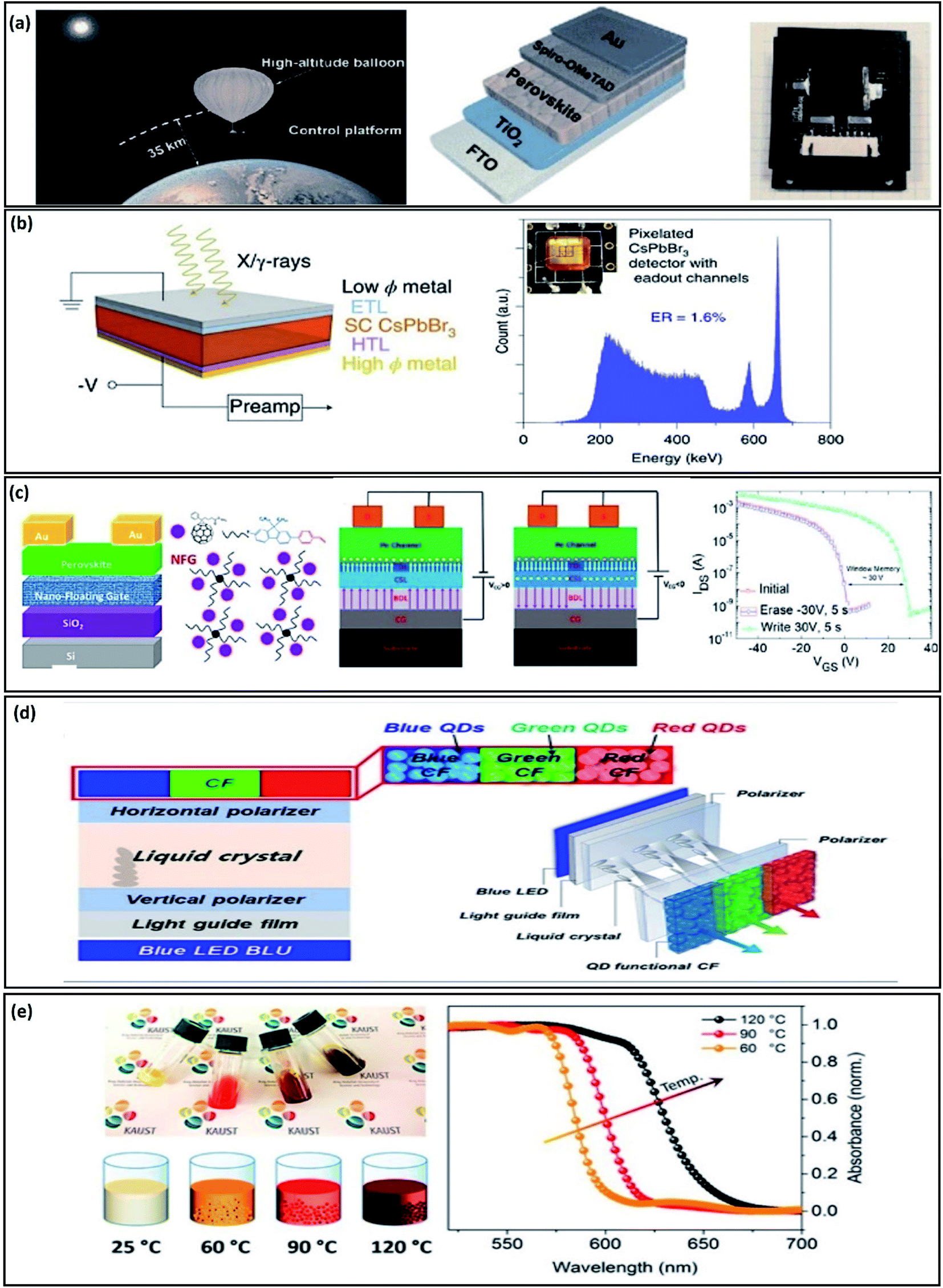 | ||
| Fig. 10 Novel applications of perovskites. (a) Stability experiment of a PSC in near space. Reproduced with permission from ref. 135 Copyright 2019 Science China Press and Springer-Verlag GmbH Germany, part of Springer Nature (b) Gamma-ray detector based on a CsPbBr3 single crystal. Reproduced with permission from ref. 137 Copyright 2021 Springer Nature SharedIt. (c) Device configuration for a perovskite-based flash memory device. Reproduced with permission from ref. 138 Copyright 2020 American Chemical Society. (d) Scheme of an LCD based on perovskite QDs. Reproduced with permission from ref. 122https://creativecommons.org/licenses/by/4.0/. (e) Thermochromic properties of perovskite for smart windows. Reproduced with permission from ref. 133 Copyright 2017 American Chemical Society. | ||
Supernovae and matter falling into black holes are two examples of gamma-radiation phenomena. Gamma rays have energies several orders of magnitude above visible light and their detection is based on the effects they have on matter. It can collide with an electron and bounce off it inducing Compton scattering,136 but it can also produce photoelectric ionization. In addition, part of the high energy of gamma rays can penetrate matter directly to create an electron–positron pair. This results in an electric current that can be quantified to evaluate the energy and direction of the original gamma ray. It is here where gamma-ray detectors are required. Currently, they can be divided into two main groups, depending on their functionality nature. The first group are spectrometers, formed by scintillators or solid-state materials, to transform the gamma ray into optical or electronic signals. The second group can perform gamma-ray imaging, based on the physical principle of electron–positron production or Compton scattering.
A recent work reported by Kanatzidis and co-workers (Fig. 10b), provides evidence of gamma-ray detection through a CsPbBr3 perovskite single crystal with an energy resolution as high as 1.4% for 137Cs 662 keV γ-rays.137 Two sensing modalities were fabricated with success: first, a single crystal large-volume employing ambipolar (planar) sensing; and second, unipolar quasi-hemispherical and pixelated sensing.
Flash memory storage devices, like USB sticks, SD cards, use non-volatile memory that works by erasing data units or blocks and rewriting them at the byte level. In 2020, Nazeeruddin and co-workers reported the fabrication of a flash memory device based on a transistor channel made from a triple-cation perovskite single crystal (Fig. 9c).138 They made a 10 nm single layer of a nanofloating gate, built with organic semiconductors: polyfluorene for p-type and fullerene for n-type, that serve as the charge storage unit. The final flash memory device showed a memory window of 30 V, an on/off ratio of 9 × 10⁷, write/erase times of 50 ms and a retention time of 106 s.
Liquid crystal displays (LCDs) are commonly used in monitors for computers, flat-screen televisions or video projection systems. In LCDs the polarization-dependent transmittance of liquid crystals is changed by the application of a varying voltage. The structure of a liquid crystal is in between a crystalline solid and a liquid. They present ordered patterns but also high molecular mobilities as in liquids. Park and co-workers demonstrated a super-high-resolution LCD using perovskite QD colour filters (Fig. 9d). They put into practice the new advance in LCD technology known as BLU technology, based on a quantum dot enhancement film (QDEF). The configuration is based on a transparent film, transparent resin embedded with red and green QDs, transparent film and a blue LED source. Then, they fabricate blue, green and red QD-functional colour filters (CFs) by using core-structure perovskite QDs, demonstrating a high PLQY and a narrow full-width at a half maximum (FWHM).139
The main application of thermochromic material is to determine temperature variations and reaction heats in chemical reactions. However, their properties can be used on a larger scale for energy-saving applications in so-called smart windows which can switch the transmittance of incident light between transparent and opaque states.140 The opto-thermal properties of perovskites were investigated and exploited by Bakr and co-workers who developed thermochromic perovskite inks for reversible smart windows applications (Fig. 9e).141 They made use of the inverse temperature crystallization (ITC) process: the temperature for crystallization depends on the halide (X: I, Br) constituents, tuning from yellow, orange, red and black while increasing the temperature and iodine content concerning bromine. They confirm the chromatic variation of the perovskite materials by measuring the absorption spectra at different temperatures; 597 nm for 60 °C, 615 nm for 90 °C and 651 nm for 120 °C, respectively.
5. Conclusions and prospects
The impressive advances of perovskite-based solar cells presage applications beyond photovoltaics. For example, PeLEDs have an impressive PLQY approaching 100% and EQEs surpassing 20% using morphology control or charge injection management. These strategies have led to the improvement of low-dimensionality structures, nanometre-size colloidal NCs, high control of radiative recombination or defect passivation. However, the operational stability of PeLEDS remains insufficient, especially in the case of the lower dimensions (2D). The ionic migration and interfacial reactions limit their lifetime to ∼200 hours. Another main challenge lies in the blue emission spectra. The current blue PeLEDs approaching 11% EQE, in the most successful case, still need to enhance carrier transport which is related to the film quality. Regarding lasing, perovskites exhibit good performance due to compositional strategies, in tuneable, multicolour and, recently, even in continuous-wave (CW) lasers, which is considered the first step to develop an electrically driven perovskite laser. With regard to structural engineering, perovskite can also be used as single-mode laser and microarrays.High sensitivity, rapid response/recovery time and low electrical or optical signal hysteresis are the crucial properties for an ideal sensor. Typically, conventional materials for sensing applications still suffer from complicated synthesis procedures, a narrow working range, and low sensitivity. In contrast, perovskite materials have shown great potential as an appropriate alternative for conventional sensors due to the ease of processing, excellent optoelectronic properties, and high sensitivity to various elements. However, one of the significant challenges of perovskite materials is their intrinsic instability. Therefore, perovskite materials should be well encapsulated or stored in an inert atmosphere and at room temperature to keep their original properties and avoid degradation.
Moreover, the ionic nature of perovskite materials makes them unstable when even traces of polar solvents are present. These disadvantages have been converted into advantages by using these materials as sensors including sensing of humidity, temperature and gases. First, the interaction between different molecules and the perovskite crystal lattice are discussed to understand perovskite sensing properties. Regarding humidity sensing, the resistance, capacitance and photoluminescence measurements are categorized as useful techniques for this property of perovskite materials. Perovskites can sense the humidity from 7% to 98% with a reversible behaviour by decreasing the moisture, which is reasonably necessary for an ideal humidity sensor. Additionally, the thermal sensing of perovskite materials due to the phase instability of perovskite materials at different temperatures are discussed. Photoluminescence spectroscopy is highlighted as a powerful method for the characterization of this property. Perovskite materials can sense a wide temperature range of 0–230 °C, introducing them as an ideal candidate temperature sensor. Regarding gas sensors, perovskite materials have excellent potential at room temperature, contrasting most traditional gas sensors, which can operate only at high temperatures. Moreover, perovskite materials can sense a wide range of gases including NH3, O2, O3 and HCl. Finally, thanks to the ionic nature of perovskite materials, it is possible to detect with high sensitivity, solvents such as THF, DMF, H2O, etc.
In addition to encouraging advances as emitting and sensing devices, novel roles such as LCDs, smart windows, store data or space applications, broaden the range of technological possibilities that perovskites offer.
Conflicts of interest
There are no conflicts to declare.Acknowledgements
M. S. thanks the German Research Foundation (DFG) for funding (SPP2196, GRK 2642). C. A. A. and M. M. B. thank the Helmholtz Young Investigator Group FRONTRUNNER. M. S. acknowledges funding by ProperPhotoMile. Project ProperPhotoMile is supported under the umbrella of SOLAR-ERA.NET Cofound 2 by The Spanish Ministry of Science and Education and the AEI under the project PCI2020-112185 and CDTI project number IDI-20210171; the Federal Ministry for Economic Affairs and Energy based on a decision by the German Bundestag project number FKZ 03EE1070B and FKZ 03EE1070A and the Israel Ministry of Energy with project number 220-11-031. SOLAR-ERA.NET is supported by the European Commission within the EU Framework Programme for Research and Innovation HORIZON 2020 (Cofound ERA-NET Action, No. 786483).References
- A. Kojima, K. Teshima, Y. Shirai and T. Miyasaka, J. Am. Chem. Soc., 2009, 131, 6050–6051 CrossRef CAS.
- L. Schmidt-Mende, V. Dyakonov, S. Olthof, F. Ünlü, K. M. T. Lê, S. Mathur, A. D. Karabanov, D. C. Lupascu, L. M. Herz, A. Hinderhofer, F. Schreiber, A. Chernikov, D. A. Egger, O. Shargaieva, C. Cocchi, E. Unger, M. Saliba, M. M. Byranvand, M. Kroll, F. Nehm, K. Leo, A. Redinger, J. Höcker, T. Kirchartz, J. Warby, E. Gutierrez-Partida, D. Neher, M. Stolterfoht, U. Würfel, M. Unmüssig, J. Herterich, C. Baretzky, J. Mohanraj, M. Thelakkat, C. Maheu, W. Jaegermann, T. Mayer, J. Rieger, T. Fauster, D. Niesner, F. Yang, S. Albrecht, T. Riedl, A. Fakharuddin, M. Vasilopoulou, Y. Vaynzof, D. Moia, J. Maier, M. Franckevičius, V. Gulbinas, R. A. Kerner, L. Zhao, B. P. Rand, N. Glück, T. Bein, F. Matteocci, L. A. Castriotta, A. D. Carlo, M. Scheffler and C. Draxl, APL Mater., 2021, 9, 109202 CrossRef CAS.
- J. J. Yoo, G. Seo, M. R. Chua, T. G. Park, Y. Lu, F. Rotermund, Y.-K. Kim, C. S. Moon, N. J. Jeon, J.-P. Correa-Baena, V. Bulović, S. S. Shin, M. G. Bawendi and J. Seo, Nature, 2021, 590, 587–593 CrossRef CAS.
- M. Jeong, I. W. Choi, E. M. Go, Y. Cho, M. Kim, B. Lee, S. Jeong, Y. Jo, H. W. Choi, J. Lee, J. H. Bae, S. K. Kwak, D. S. Kim and C. Yang, Science, 2020, 369, 1615–1620 CrossRef CAS PubMed.
- I. E. Agency, World Energy Outlook 2020, 2020 Search PubMed.
- M. Green, E. Dunlop, J. Hohl-Ebinger, M. Yoshita, N. Kopidakis and X. Hao, Prog. Photovoltaics, 2021, 29, 3–15 Search PubMed.
- N.-G. Park, Mater. Today, 2015, 18, 65–72 CrossRef CAS.
- Z. Saki, M. M. Byranvand, N. Taghavinia, M. Kedia and M. Saliba, Energy Environ. Sci., 2021, 14, 5690–5722 RSC.
- M. L. Petrus, J. Schlipf, C. Li, T. P. Gujar, N. Giesbrecht, P. Müller-Buschbaum, M. Thelakkat, T. Bein, S. Hüttner and P. Docampo, Adv. Energy Mater., 2017, 7, 1700264 CrossRef.
- J.-P. Correa-Baena, M. Saliba, T. Buonassisi, M. Grätzel, A. Abate, W. Tress and A. Hagfeldt, Science, 2017, 358, 739 CrossRef CAS PubMed.
- S. Y. Park, J.-S. Park, B. J. Kim, H. Lee, A. Walsh, K. Zhu, D. H. Kim and H. S. Jung, Nat. Sustain., 2020, 3, 1044–1051 CrossRef.
- B. Shi, L. Duan, Y. Zhao, J. Luo and X. Zhang, Adv. Mater., 2020, 32, 1806474 CrossRef CAS PubMed.
- M. Saliba, J.-P. Correa-Baena, M. Grätzel, A. Hagfeldt and A. Abate, Angew. Chem., Int. Ed., 2018, 57, 2554–2569 CrossRef CAS PubMed.
- J. Bisquert, G. García-Belmonte and I. Mora-Sero, Unconventional Thin Film Photovoltaics, 2016, pp. 57–106 Search PubMed.
- J. Qin, X.-K. Liu, C. Yin and F. Gao, Trends Chem., 2021, 3, 34–46 CrossRef CAS.
- H. Dong, C. Zhang, X. Liu, J. Yao and Y. S. Zhao, Chem. Soc. Rev., 2020, 49, 951–982 RSC.
- C. C. Boyd, R. Cheacharoen, T. Leijtens and M. D. McGehee, Chem. Rev., 2019, 119, 3418–3451 CrossRef CAS.
- J. Ye, M. M. Byranvand, C. O. Martínez, R. L. Z. Hoye, M. Saliba and L. Polavarapu, Angew. Chem., Int. Ed., 2021, 133, 21804–21828 CrossRef.
- J. Lee, M. Malekshahi Byranvand, G. Kang, S. Y. Son, S. Song, G.-W. Kim and T. Park, J. Am. Chem. Soc., 2017, 139, 12175–12181 CrossRef CAS PubMed.
- M. Saliba, T. Matsui, J.-Y. Seo, K. Domanski, J.-P. Correa-Baena, M. K. Nazeeruddin, S. M. Zakeeruddin, W. Tress, A. Abate, A. Hagfeldt and M. Grätzel, Energy Environ. Sci., 2016, 9, 1989–1997 RSC.
- M. Saliba, T. Matsui, K. Domanski, J. Y. Seo, A. Ummadisingu, S. M. Zakeeruddin, J. P. Correa-Baena, W. R. Tress, A. Abate, A. Hagfeldt and M. Grätzel, Science, 2016, 354, 206–209 CrossRef CAS.
- Y. Zhao, J. Wei, H. Li, Y. Yan, W. Zhou, D. Yu and Q. Zhao, Nat. Commun., 2016, 7, 10228 CrossRef CAS.
- M. Malekshahi Byranvand, F. Behboodi-Sadabad, A. Alrhman Eliwi, V. Trouillet, A. Welle, S. Ternes, I. M. Hossain, M. R. Khan, J. A. Schwenzer, A. Farooq, B. S. Richards, J. Lahann and U. W. Paetzold, J. Mater. Chem. A, 2020, 8, 20122–20132 RSC.
- J. Lee, T. H. Lee, M. M. Byranvand, K. Choi, H. I. Kim, S. A. Park, J. Y. Kim and T. Park, J. Mater. Chem. A, 2018, 6, 5538–5543 RSC.
- M. V. Khenkin, E. A. Katz, A. Abate, G. Bardizza, J. J. Berry, C. Brabec, F. Brunetti, V. Bulović, Q. Burlingame, A. Di Carlo, R. Cheacharoen, Y.-B. Cheng, A. Colsmann, S. Cros, K. Domanski, M. Dusza, C. J. Fell, S. R. Forrest, Y. Galagan, D. Di Girolamo, M. Grätzel, A. Hagfeldt, E. von Hauff, H. Hoppe, J. Kettle, H. Köbler, M. S. Leite, S. Liu, Y.-L. Loo, J. M. Luther, C.-Q. Ma, M. Madsen, M. Manceau, M. Matheron, M. McGehee, R. Meitzner, M. K. Nazeeruddin, A. F. Nogueira, Ç. Odabaşı, A. Osherov, N.-G. Park, M. O. Reese, F. De Rossi, M. Saliba, U. S. Schubert, H. J. Snaith, S. D. Stranks, W. Tress, P. A. Troshin, V. Turkovic, S. Veenstra, I. Visoly-Fisher, A. Walsh, T. Watson, H. Xie, R. Yıldırım, S. M. Zakeeruddin, K. Zhu and M. Lira-Cantu, Nat. Energy, 2020, 5, 35–49 CrossRef.
- B. Chen, P. N. Rudd, S. Yang, Y. Yuan and J. Huang, Chem. Soc. Rev., 2019, 48, 3842–3867 RSC.
- M. Saliba, J.-P. Correa-Baena, C. M. Wolff, M. Stolterfoht, N. Phung, S. Albrecht, D. Neher and A. Abate, Chem. Mater., 2018, 30, 4193–4201 CrossRef CAS.
- B. J. Kim, D. H. Kim, S. L. Kwon, S. Y. Park, Z. Li, K. Zhu and H. S. Jung, Nat. Commun., 2016, 7, 11735 CrossRef CAS PubMed.
- C. Pi, X. Yu, W. Chen, L. Yang, C. Wang, Z. Liu, Y. Wang, J. Qiu, B. Liu and X. Xu, Mater. Adv., 2021, 2, 1043–1049 RSC.
- A. Tejeda, W. C. H. Choy, E. Deleporte and M. Grätzel, J. Phys. D: Appl. Phys., 2019, 53, 070201 CrossRef.
- Z. Xu, X. Liu, Y. Li, X. Liu, T. Yang, C. Ji, S. Han, Y. Xu, J. Luo and Z. Sun, Angew. Chem., Int. Ed., 2019, 58, 15757–15761 CrossRef CAS PubMed.
- M. Auf der Maur, A. Pecchia, G. Penazzi, W. Rodrigues and A. Di Carlo, Phys. Rev. Lett., 2016, 116, 027401 CrossRef PubMed.
- M. Z. Baten, S. Alam, B. Sikder and A. Aziz, Photonics, 2021, 8, 430 CrossRef CAS.
- J. Cho, J. H. Park, J. K. Kim and E. F. Schubert, Laser Photonics Rev., 2017, 11, 1600147 CrossRef.
- Q. Zhang, L. Chu, F. Zhou, W. Ji and G. Eda, Adv. Mater., 2018, 30, 1704055 CrossRef.
- A. K. Jena, A. Kulkarni and T. Miyasaka, Chem. Rev., 2019, 119, 3036–3103 CrossRef CAS PubMed.
- T. Kirchartz, L. Krückemeier and E. L. Unger, APL Mater., 2018, 6, 100702 CrossRef.
- S. D. Stranks, V. M. Burlakov, T. Leijtens, J. M. Ball, A. Goriely and H. J. Snaith, Phys. Rev. Appl., 2014, 2, 034007 CrossRef CAS.
- Z.-K. Tan, R. S. Moghaddam, M. L. Lai, P. Docampo, R. Higler, F. Deschler, M. Price, A. Sadhanala, L. M. Pazos, D. Credgington, F. Hanusch, T. Bein, H. J. Snaith and R. H. Friend, Nat. Nanotechnol., 2014, 9, 687–692 CrossRef CAS.
- Y. Cao, N. Wang, H. Tian, J. Guo, Y. Wei, H. Chen, Y. Miao, W. Zou, K. Pan, Y. He, H. Cao, Y. Ke, M. Xu, Y. Wang, M. Yang, K. Du, Z. Fu, D. Kong, D. Dai, Y. Jin, G. Li, H. Li, Q. Peng, J. Wang and W. Huang, Nature, 2018, 562, 249–253 CrossRef CAS PubMed.
- H. Cho, S.-H. Jeong, M.-H. Park, Y.-H. Kim, C. Wolf, C.-L. Lee, J. H. Heo, A. Sadhanala, N. Myoung, S. Yoo, S. H. Im, R. H. Friend and T.-W. Lee, Science, 2015, 350, 1222–1225 CrossRef CAS PubMed.
- H. Cho, J. S. Kim, C. Wolf, Y.-H. Kim, H. J. Yun, S.-H. Jeong, A. Sadhanala, V. Venugopalan, J. W. Choi, C.-L. Lee, R. H. Friend and T.-W. Lee, ACS Nano, 2018, 12, 2883–2892 CrossRef CAS PubMed.
- M. Yuan, L. N. Quan, R. Comin, G. Walters, R. Sabatini, O. Voznyy, S. Hoogland, Y. Zhao, E. M. Beauregard, P. Kanjanaboos, Z. Lu, D. H. Kim and E. H. Sargent, Nat. Nanotechnol., 2016, 11, 872–877 CrossRef CAS PubMed.
- N. Wang, L. Cheng, R. Ge, S. Zhang, Y. Miao, W. Zou, C. Yi, Y. Sun, Y. Cao, R. Yang, Y. Wei, Q. Guo, Y. Ke, M. Yu, Y. Jin, Y. Liu, Q. Ding, D. Di, L. Yang, G. Xing, H. Tian, C. Jin, F. Gao, R. H. Friend, J. Wang and W. Huang, Nat. Photonics, 2016, 10, 699–704 CrossRef CAS.
- Y. Sun, L. Zhang, N. Wang, S. Zhang, Y. Cao, Y. Miao, M. Xu, H. Zhang, H. Li, C. Yi, J. Wang and W. Huang, npj Flexible Electron., 2018, 2, 12 CrossRef.
- Z. Xiao, R. A. Kerner, L. Zhao, N. L. Tran, K. M. Lee, T.-W. Koh, G. D. Scholes and B. P. Rand, Nat. Photonics, 2017, 11, 108–115 CrossRef CAS.
- L. Protesescu, S. Yakunin, M. I. Bodnarchuk, F. Krieg, R. Caputo, C. H. Hendon, R. X. Yang, A. Walsh and M. V. Kovalenko, Nano Lett., 2015, 15, 3692–3696 CrossRef CAS.
- G. Li, F. W. R. Rivarola, N. J. L. K. Davis, S. Bai, T. C. Jellicoe, F. de la Peña, S. Hou, C. Ducati, F. Gao, R. H. Friend, N. C. Greenham and Z.-K. Tan, Adv. Mater., 2016, 28, 3528–3534 CrossRef CAS PubMed.
- J. Song, J. Li, X. Li, L. Xu, Y. Dong and H. Zeng, Adv. Mater., 2015, 27, 7162–7167 CrossRef CAS.
- J. Li, L. Xu, T. Wang, J. Song, J. Chen, J. Xue, Y. Dong, B. Cai, Q. Shan, B. Han and H. Zeng, Adv. Mater., 2017, 29, 1603885 CrossRef.
- L. Protesescu, S. Yakunin, S. Kumar, J. Bär, F. Bertolotti, N. Masciocchi, A. Guagliardi, M. Grotevent, I. Shorubalko, M. I. Bodnarchuk, C.-J. Shih and M. V. Kovalenko, ACS Nano, 2017, 11, 3119–3134 CrossRef CAS.
- Y. H. Kim, C. Wolf, Y. T. Kim, H. Cho, W. Kwon, S. Do, A. Sadhanala, C. G. Park, S. W. Rhee, S. H. Im, R. H. Friend and T. W. Lee, ACS Nano, 2017, 11, 6586–6593 CrossRef CAS.
- W. Xu, Q. Hu, S. Bai, C. Bao, Y. Miao, Z. Yuan, T. Borzda, A. J. Barker, E. Tyukalova, Z. Hu, M. Kawecki, H. Wang, Z. Yan, X. Liu, X. Shi, K. Uvdal, M. Fahlman, W. Zhang, M. Duchamp, J.-M. Liu, A. Petrozza, J. Wang, L.-M. Liu, W. Huang and F. Gao, Nat. Photonics, 2019, 13, 418–424 CrossRef CAS.
- T. Chiba, Y. Hayashi, H. Ebe, K. Hoshi, J. Sato, S. Sato, Y.-J. Pu, S. Ohisa and J. Kido, Nat. Photonics, 2018, 12, 681–687 CrossRef CAS.
- K. Lin, J. Xing, L. N. Quan, F. P. G. de Arquer, X. Gong, J. Lu, L. Xie, W. Zhao, D. Zhang, C. Yan, W. Li, X. Liu, Y. Lu, J. Kirman, E. H. Sargent, Q. Xiong and Z. Wei, Nature, 2018, 562, 245–248 CrossRef CAS.
- M. Karlsson, Z. Yi, S. Reichert, X. Luo, W. Lin, Z. Zhang, C. Bao, R. Zhang, S. Bai, G. Zheng, P. Teng, L. Duan, Y. Lu, K. Zheng, T. Pullerits, C. Deibel, W. Xu, R. Friend and F. Gao, Nat. Commun., 2021, 12, 361 CrossRef CAS PubMed.
- Z. Yuan, C. Zhou, Y. Tian, Y. Shu, J. Messier, J. C. Wang, L. J. van de Burgt, K. Kountouriotis, Y. Xin, E. Holt, K. Schanze, R. Clark, T. Siegrist and B. Ma, Nat. Commun., 2017, 8, 14051 CrossRef CAS PubMed.
- M. D. Smith and H. I. Karunadasa, Acc. Chem. Res., 2018, 51, 619–627 CrossRef CAS.
- Q. Dong, L. Lei, J. Mendes and F. So, J. Phys.: Mater., 2020, 3, 012002 CAS.
- G. Li, K. Chen, Y. Cui, Y. Zhang, Y. Tian, B. Tian, Y. Hao, Y. Wu and H. Zhang, Adv. Opt. Mater., 2020, 8, 1902012 CrossRef CAS.
- X. Dai, Z. Zhang, Y. Jin, Y. Niu, H. Cao, X. Liang, L. Chen, J. Wang and X. Peng, Nature, 2014, 515, 96–99 CrossRef CAS PubMed.
- H. P. Kim, J. Kim, B. S. Kim, H.-M. Kim, J. Kim, A. R. b. M. Yusoff, J. Jang and M. K. Nazeeruddin, Adv. Opt. Mater., 2017, 5, 1600920 CrossRef.
- L. N. Quan, M. Yuan, R. Comin, O. Voznyy, E. M. Beauregard, S. Hoogland, A. Buin, A. R. Kirmani, K. Zhao, A. Amassian, D. H. Kim and E. H. Sargent, J. Am. Chem. Soc., 2016, 138, 2649–2655 CrossRef CAS PubMed.
- Y. Tian, C. Zhou, M. Worku, X. Wang, Y. Ling, H. Gao, Y. Zhou, Y. Miao, J. Guan and B. Ma, Adv. Mater., 2018, 30, 1707093 CrossRef PubMed.
- B. Zhao, S. Bai, V. Kim, R. Lamboll, R. Shivanna, F. Auras, J. M. Richter, L. Yang, L. Dai, M. Alsari, X.-J. She, L. Liang, J. Zhang, S. Lilliu, P. Gao, H. J. Snaith, J. Wang, N. C. Greenham, R. H. Friend and D. Di, Nat. Photonics, 2018, 12, 783–789 CrossRef CAS.
- Z. Andaji-Garmaroudi, M. Anaya, A. J. Pearson and S. D. Stranks, Adv. Energy Mater., 2020, 10, 1903109 CrossRef CAS.
- T.-H. Han, J.-W. Lee, Y. J. Choi, C. Choi, S. Tan, S.-J. Lee, Y. Zhao, Y. Huang, D. Kim and Y. Yang, Adv. Mater., 2020, 32, 2070007 CrossRef.
- C. Aranda, A. Guerrero and J. Bisquert, ACS Energy Lett., 2019, 4, 741–746 CrossRef CAS.
- J. H. Park, A.-y. Lee, J. C. Yu, Y. S. Nam, Y. Choi, J. Park and M. H. Song, ACS Appl. Mater. Interfaces, 2019, 11, 8428–8435 CrossRef CAS PubMed.
- I. D. W. Samuel, E. B. Namdas and G. A. Turnbull, Nat. Photonics, 2009, 3, 546–549 CrossRef CAS.
- K. K. Ng and S. M. Sze, Physics of Semiconductor Devices, John Wiley & Sons, Inc., 2006 Search PubMed.
- M. Ito, T. Ito and T. Kimura, J. Appl. Phys., 1979, 50, 6168–6174 CrossRef CAS.
- C. Cho, T. Antrack, M. Kroll, Q. An, T. R. Bärschneider, A. Fischer, S. Meister, Y. Vaynzof and K. Leo, Adv. Sci., 2021, 8, 2101663 CrossRef CAS PubMed.
- B. R. Sutherland and E. H. Sargent, Nat. Photonics, 2016, 10, 295–302 CrossRef CAS.
- G. Xing, N. Mathews, S. S. Lim, N. Yantara, X. Liu, D. Sabba, M. Grätzel, S. Mhaisalkar and T. C. Sum, Nat. Mater., 2014, 13, 476–480 CrossRef CAS.
- M. J. Colles and C. R. Pidgeon, Rep. Prog. Phys., 1975, 38, 329–460 CrossRef CAS.
- J. R. Taylor, Opt. Acta, 1985, 32, 1450 CrossRef.
- P. F. Moulton, Proc. IEEE, 1992, 80, 348–364 CrossRef CAS.
- C. J. Hawthorn, K. P. Weber and R. E. Scholten, Rev. Sci. Instrum., 2001, 72, 4477–4479 CrossRef CAS.
- B. Tang, Y. Hu, J. Lu, H. Dong, N. Mou, X. Gao, H. Wang, X. Jiang and L. Zhang, Nano Energy, 2020, 71, 104641 CrossRef CAS.
- M. H. Huang, S. Mao, H. Feick, H. Yan, Y. Wu, H. Kind, E. Weber, R. Russo and P. Yang, Science, 2001, 292, 1897–1899 CrossRef CAS PubMed.
- C. Dang, J. Lee, C. Breen, J. S. Steckel, S. Coe-Sullivan and A. Nurmikko, Nat. Nanotechnol., 2012, 7, 335–339 CrossRef CAS PubMed.
- C. H. Lin, Q. Zeng, E. Lafalce, S. Yu, M. J. Smith, Y. J. Yoon, Y. Chang, Y. Jiang, Z. Lin, Z. V. Vardeny and V. V. Tsukruk, Adv. Opt. Mater., 2018, 6, 1800474 CrossRef.
- A. Javan, W. R. Bennett and D. R. Herriott, Phys. Rev. Lett., 1961, 6, 106–110 CrossRef CAS.
- J. S. Manser, J. A. Christians and P. V. Kamat, Chem. Rev., 2016, 116, 12956–13008 CrossRef CAS PubMed.
- C. Qin, A. S. D. Sandanayaka, C. Zhao, T. Matsushima, D. Zhang, T. Fujihara and C. Adachi, Nature, 2020, 585, 53–57 CrossRef CAS PubMed.
- M. A. Baldo, R. J. Holmes and S. R. Forrest, Phys. Rev. B: Condens. Matter Mater. Phys., 2002, 66, 035321 CrossRef.
- A. Polynkin, P. Polynkin, M. Mansuripur and N. Peyghambarian, Opt. Express, 2005, 13, 3179–3184 CrossRef PubMed.
- C. Zhou, J. Yu, H. Dong, F. Yuan, X. Zheng, M. Jiang and L. Zhang, J. Mater. Chem. C, 2020, 8, 13642–13647 RSC.
- K. Wang, Y. Du, J. Liang, J. Zhao, F. F. Xu, X. Liu, C. Zhang, Y. Yan and Y. S. Zhao, Adv. Mater., 2020, 32, 2001999 CrossRef CAS.
- Z. Zhu, Q. Sun, Z. Zhang, J. Dai, G. Xing, S. Li, X. Huang and W. Huang, J. Mater. Chem. C, 2018, 6, 10121–10137 RSC.
- Z. Chen and C. Lu, Sens. Lett., 2005, 3, 274–295 CrossRef CAS.
- R. Malik, V. K. Tomer, V. Chaudhary, M. S. Dahiya, A. Sharma, S. P. Nehra, S. Duhan and K. Kailasam, J. Mater. Chem. A, 2017, 5, 14134–14143 RSC.
- T. Seiyama, N. Yamazoe and H. Arai, Sens. Actuators, 1983, 4, 85–96 CrossRef CAS.
- Z. Li, B. Zhang, K. Li, T. Zhang and X. Yang, J. Mater. Chem. C, 2020, 8, 3088–3096 RSC.
- M. M. Lee, J. Teuscher, T. Miyasaka, T. N. Murakami and H. J. Snaith, Science, 2012, 338, 643–647 CrossRef CAS PubMed.
- Z. Zhu, V. G. Hadjiev, Y. Rong, R. Guo, B. Cao, Z. Tang, F. Qin, Y. Li, Y. Wang, F. Hao, S. Venkatesan, W. Li, S. Baldelli, A. M. Guloy, H. Fang, Y. Hu, Y. Yao, Z. Wang and J. Bao, Chem. Mater., 2016, 28, 7385–7393 CrossRef CAS.
- J. A. Christians, P. A. Miranda Herrera and P. V. Kamat, J. Am. Chem. Soc., 2015, 137, 1530–1538 CrossRef CAS PubMed.
- L. Hu, G. Shao, T. Jiang, D. Li, X. Lv, H. Wang, X. Liu, H. Song, J. Tang and H. Liu, ACS Appl. Mater. Interfaces, 2015, 7, 25113–25120 CrossRef CAS PubMed.
- K. Ren, L. Huang, S. Yue, S. Lu, K. Liu, M. Azam, Z. Wang, Z. Wei, S. Qu and Z. Wang, J. Mater. Chem. C, 2017, 5, 2504–2508 RSC.
- M.-Y. Cho, S. Kim, I.-S. Kim, E.-S. Kim, Z.-J. Wang, N.-Y. Kim, S.-W. Kim and J.-M. Oh, Adv. Funct. Mater., 2020, 30, 1907449 CrossRef CAS.
- W. Xu, F. Li, Z. Cai, Y. Wang, F. Luo and X. Chen, J. Mater. Chem. C, 2016, 4, 9651–9655 RSC.
- A. E. Maughan, A. M. Ganose, M. M. Bordelon, E. M. Miller, D. O. Scanlon and J. R. Neilson, J. Am. Chem. Soc., 2016, 138, 8453–8464 CrossRef CAS PubMed.
- B. Lee, C. C. Stoumpos, N. Zhou, F. Hao, C. Malliakas, C.-Y. Yeh, T. J. Marks, M. G. Kanatzidis and R. P. H. Chang, J. Am. Chem. Soc., 2014, 136, 15379–15385 CrossRef CAS PubMed.
- A. H. Slavney, T. Hu, A. M. Lindenberg and H. I. Karunadasa, J. Am. Chem. Soc., 2016, 138, 2138–2141 CrossRef CAS PubMed.
- G. Volonakis, M. R. Filip, A. A. Haghighirad, N. Sakai, B. Wenger, H. J. Snaith and F. Giustino, J. Phys. Chem. Lett., 2016, 7, 1254–1259 CrossRef CAS PubMed.
- E. T. McClure, M. R. Ball, W. Windl and P. M. Woodward, Chem. Mater., 2016, 28, 1348–1354 CrossRef CAS.
- B. Lee, C. C. Stoumpos, N. Zhou, F. Hao, C. Malliakas, C. Y. Yeh, T. J. Marks, M. G. Kanatzidis and R. P. Chang, J. Am. Chem. Soc., 2014, 136, 15379–15385 CrossRef CAS PubMed.
- Z. Weng, J. Qin, A. A. Umar, J. Wang, X. Zhang, H. Wang, X. Cui, X. Li, L. Zheng and Y. Zhan, Adv. Funct. Mater., 2019, 29, 1902234 CrossRef.
- N. Sakai, A. A. Haghighirad, M. R. Filip, P. K. Nayak, S. Nayak, A. Ramadan, Z. Wang, F. Giustino and H. J. Snaith, J. Am. Chem. Soc., 2017, 139, 6030–6033 CrossRef CAS PubMed.
- W. Ye, Q. Cao, X.-F. Cheng, C. Yu, J.-H. He and J.-M. Lu, J. Mater. Chem. A, 2020, 8, 17675–17682 RSC.
- X.-d. Wang, O. S. Wolfbeis and R. J. Meier, Chem. Soc. Rev., 2013, 42, 7834–7869 RSC.
- B. Arman Kuzubasoglu and S. Kursun Bahadir, Sens. Actuators, A, 2020, 315, 112282 CrossRef CAS.
- P. R. N. Childs, J. R. Greenwood and C. A. Long, Rev. Sci. Instrum., 2000, 71, 2959–2978 CrossRef CAS.
- B. Lee, Opt. Fiber Technol., 2003, 9, 57–79 CrossRef CAS.
- T. L. Packham, D. Fok, K. Frederiksen, L. Thabane and N. Buckley, J. Hand Ther., 2012, 25, 358–361 CrossRef PubMed ; quiz 362..
- M. D. Dramićanin, J. Appl. Phys., 2020, 128, 040902 CrossRef.
- Y. Niu, F. Zhang, Z. Bai, Y. Dong, J. Yang, R. Liu, B. Zou, J. Li and H. Zhong, Adv. Opt. Mater., 2015, 3, 112–119 CrossRef CAS.
- D. Zhang, Y. Xu, Q. Liu and Z. Xia, Inorg. Chem., 2018, 57, 4613–4619 CrossRef CAS PubMed.
- M. B. Faheem, B. Khan, C. Feng, M. U. Farooq, F. Raziq, Y. Xiao and Y. Li, ACS Energy Lett., 2020, 5, 290–320 CrossRef CAS.
- B. Zhuang, Y. Liu, S. Yuan, H. Huang, J. Chen and D. Chen, Nanoscale, 2019, 11, 15010–15016 RSC.
- A. Dey, Mater. Sci. Eng., C, 2018, 229, 206–217 CrossRef CAS.
- P. Rai, R. Khan, S. Raj, S. M. Majhi, K.-K. Park, Y.-T. Yu, I.-H. Lee and P. K. Sekhar, Nanoscale, 2014, 6, 581–588 RSC.
- M. Xue, F. Li, D. Chen, Z. Yang, X. Wang and J. Ji, Adv. Mater., 2016, 28, 8265–8270 CrossRef CAS.
- Y. Zhao and K. Zhu, Chem. Commun., 2014, 50, 1605–1607 RSC.
- C. Bao, J. Yang, W. Zhu, X. Zhou, H. Gao, F. Li, G. Fu, T. Yu and Z. Zou, Chem. Commun., 2015, 51, 15426–15429 RSC.
- M.-A. Stoeckel, M. Gobbi, S. Bonacchi, F. Liscio, L. Ferlauto, E. Orgiu and P. Samorì, Adv. Mater., 2017, 29, 1702469 CrossRef.
- H. Chen, M. Zhang, R. Bo, C. Barugkin, J. Zheng, Q. Ma, S. Huang, A. W. Y. Ho-Baillie, K. R. Catchpole and A. Tricoli, Small, 2018, 14, 1702571 CrossRef PubMed.
- K. Brintakis, E. Gagaoudakis, A. Kostopoulou, V. Faka, A. Argyrou, V. Binas, G. Kiriakidis and E. Stratakis, Nanoscale Adv., 2019, 1, 2699–2706 RSC.
- X. Chen, H. Hu, Z. Xia, W. Gao, W. Gou, Y. Qu and Y. Ma, J. Mater. Chem. C, 2017, 5, 309–313 RSC.
- M. Aamir, M. Sher, M. A. Malik, N. Revaprasadu and J. Akhtar, Mater. Lett., 2016, 183, 135–138 CrossRef CAS.
- M. Ralaiarisoa, Y. Rodríguez, I. Salzmann, L. Vaillant and N. Koch, Appl. Phys. A: Mater. Sci. Process., 2019, 125, 470 CrossRef CAS.
- S. Kang, J. Jeong, S. Cho, Y. J. Yoon, S. Park, S. Lim, J. Y. Kim and H. Ko, J. Mater. Chem. A, 2019, 7, 1107–1114 RSC.
- N. Klein-Kedem, D. Cahen and G. Hodes, Acc. Chem. Res., 2016, 49, 347–354 CrossRef CAS PubMed.
- Y. Tu, G. Xu, X. Yang, Y. Zhang, Z. Li, R. Su, D. Luo, W. Yang, Y. Miao, R. Cai, L. Jiang, X. Du, Y. Yang, Q. Liu, Y. Gao, S. Zhao, W. Huang, Q. Gong and R. Zhu, Sci. China: Phys., Mech. Astron., 2019, 62, 974221 Search PubMed.
- T. Maruyama, T. Hayakawa and T. Kajino, Sci. Rep., 2019, 9, 7998 CrossRef PubMed.
- Y. He, M. Petryk, Z. Liu, D. G. Chica, I. Hadar, C. Leak, W. Ke, I. Spanopoulos, W. Lin, D. Y. Chung, B. W. Wessels, Z. He and M. G. Kanatzidis, Nat. Photonics, 2021, 15, 36–42 CrossRef CAS.
- M. Vasilopoulou, B. S. Kim, H. P. Kim, W. J. da Silva, F. K. Schneider, M. A. Mat Teridi, P. Gao, A. R. b. Mohd Yusoff and M. K. Nazeeruddin, Nano Lett., 2020, 20, 5081–5089 CrossRef CAS PubMed.
- Y.-H. Ko, M. Jalalah, S.-J. Lee and J.-G. Park, Sci. Rep., 2018, 8, 12881 CrossRef PubMed.
- Y. Wang, E. L. Runnerstrom and D. J. Milliron, Annu. Rev. Chem. Biomol. Eng., 2016, 7, 283–304 CrossRef CAS PubMed.
- M. De Bastiani, M. I. Saidaminov, I. Dursun, L. Sinatra, W. Peng, U. Buttner, O. F. Mohammed and O. M. Bakr, Chem. Mater., 2017, 29, 3367–3370 CrossRef CAS.
| This journal is © The Royal Society of Chemistry 2022 |