
 Open Access Article
 This Open Access Article is licensed under a
 Creative Commons Attribution 3.0 Unported Licence
Silver niobate perovskites: structure, properties and multifunctional applications
Ye
Tian
 *abc,
Panpan
Song
a,
Giuseppe
Viola
*cd,
Jindou
Shi
ab,
Jing
Li
b,
Li
Jin
b,
Qingyuan
Hu
b,
Yonghao
Xu
e,
Wanyin
Ge
a,
Zhongna
Yan
f,
Dou
Zhang
f,
Nadezda V.
Tarakina
g,
Isaac
Abrahams
h,
Xiaoyong
Wei
*b and
Haixue
Yan
*c
*abc,
Panpan
Song
a,
Giuseppe
Viola
*cd,
Jindou
Shi
ab,
Jing
Li
b,
Li
Jin
b,
Qingyuan
Hu
b,
Yonghao
Xu
e,
Wanyin
Ge
a,
Zhongna
Yan
f,
Dou
Zhang
f,
Nadezda V.
Tarakina
g,
Isaac
Abrahams
h,
Xiaoyong
Wei
*b and
Haixue
Yan
*c
aSchool of Materials Science & Engineering, Shaanxi University of Science & Technology, Xi'an, 710021, China. E-mail: ye.tian@sust.edu.cn
bElectronic Materials Research Laboratory, Key Laboratory of the Ministry of Education, School of Electronic Science and Engineering, Xi'an Jiaotong University, Xi'an 710049, China. E-mail: wdy@xjtu.edu.cn
cSchool of Engineering and Materials Science, Queen Mary University of London, Mile End Road, London E1 4NS, UK. E-mail: h.x.yan@qmul.ac.uk
dInstitute for Materials Discovery, University College London, Torrington Place, London WC1E 7JE, UK. E-mail: g.viola@ucl.ac.uk
eSchool of Physics and Electronic Information Engineering, Henan Polytechnic University, Jiaozuo 454003, China
fState Key Laboratory of Powder Metallurgy, Central South University, South Lushan Road, Changsha, 410083, China
gMax-Planck Institute of Colloids and Interfaces, Department of Colloid Chemistry, Research Campus Golm, Am Mühlenberg 1, 14476 Potsdam, Germany
hDepartment of Chemistry, Queen Mary University of London, Mile End Road, London E1 4NS, UK
First published on 17th June 2022
Abstract
AgNbO3 exhibits “peculiar” anti-/ferroelectricity and narrow bandgap semi-conductivity that lead to active responses to different types of external stimuli, including electric fields, light and mechanical forces. Some of these unique properties are also mutually coupled and could be suited for the development of multifunctional devices for a broad range of applications, including dielectric, piezoelectric, high-power energy storage/conversion, photocatalytic and photovoltaic devices. In this review, recent studies of AgNbO3 and AgNbO3-based materials are summarized. The main scope is to establish the correlations between chemical composition, synthesis conditions, structure, and properties, with an improved understanding of the phase transformations taking place in the three so called “M” phases, to ultimately provide guidance on the materials development in two key sectors: high-power energy storage and photocatalysis. Finally, current challenges in multifunctional applications and future research directions are summarized.
The present review is organized into six main sections. The first section contains a broad introduction to the generalities of AgNbO3-based ceramics and their importance within the lead-free perovskite family. Particular attention is given to the peculiar shapes of the polarization–electric field hysteresis loops, which represent one of the most fascinating aspects of these materials. The second section is dedicated to the synthesis, structure and relevant properties of AgNbO3. In particular, the initial part of this section is focused on the procedures used to fabricate bulk ceramics, single crystals and thin films and the main issues encountered in obtaining high quality products. This part is followed by an extensive discussion on the ongoing debate concerning the actual nature of the crystal structure of AgNbO3 at room temperature, during which ferroelectric, ferrielectric and antiferroelectric structures are compared and contrasted against each other. After that, a detailed survey on the polymorphic nature of AgNbO3 is presented, by summarizing the current understanding of the temperature-induced structural modifications, in relation to the anomalies found in the temperature dependence of the dielectric properties. The following part is dedicated to the shapes of the current–polarization–electric field hysteresis loops and their relationships with the electric field-induced structural transformations that take place during the application of an external electric field. The second section is concluded with a survey on the photocatalytic and photovoltaic behavior of AgNbO3. The third section is focused on the variations of crystal structure, and dielectric, ferroelectric and hysteresis loop characteristics, induced by chemical modifications using iso- and aliovalent elements. This helps outline general compositional design criteria aimed at obtaining desired properties. Sections four and five are respectively dedicated to two main applications, namely high-power energy storage and photocatalysis. The comparison of key properties obtained in different AgNbO3-based systems provides additional information on composition and processing optimization to achieve maximized properties. The review is concluded with a broad summary and outlook presented in section six, in which the main findings are concisely described to increase the focus. At the same time, open questions, outstanding issues, and future research directions that could possibly fill the current knowledge gap are discussed.
1. Introduction
Pb-containing antiferroelectric compounds such as lead zirconate can transform into ferroelectrics when they are subjected to an electric field beyond a certain threshold. During these electric-field-driven phase transitions, various properties (such as polarization and strain) exhibit significant changes.1–3 Chemically-modified Pb-based antiferroelectric materials mainly display two types of field-induced transition process.1,2 The first type is characterized by reversible double polarization–electric field hysteresis loops (Fig. 1a), while the second is distinguished by “ferroelectric-like” hysteresis loops, which are observed after an irreversible transition has taken place during the first electrical loading cycle, as shown in Fig. 1b.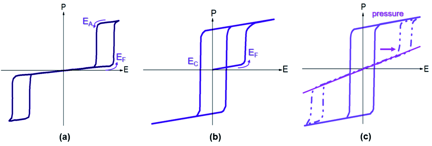 | ||
| Fig. 1 Polarization vs. electric field loops for an antiferroelectric: (a) double polarization hysteresis loop for a reversible antiferroelectric–ferroelectric (AFE–FE) transition, (b) first-poling of an antiferroelectric displaying an irreversible AFE–FE transition, and (c) P–E loop evolution under increasing in situ pressure (indicated by arrow), showing a pressured-induced transition from metastable FE to AFE. | ||
Double hysteresis loops are characterized by high charge storage density, which can be released over very short times, even in nanoseconds.4 Ferroelectric-like hysteresis loops can become “double” or even “linear” under pressure or shock pressure waves (Fig. 1c),3 and the charge stored in the electric-field-induced metastable ferroelectric state can be instantly released. These properties have allowed for the widespread application of Pb-containing antiferroelectric functional oxides in energy storage technologies, such as pulse power electronic devices,5 and in energy conversion systems, such as explosive power exchange.3,6 Moreover, the electric-field-induced anti-/ferroelectric phase transition determines the on–off properties and can provide tunable dielectric, piezoelectric, pyroelectric, and electrocaloric properties by varying the magnitude of the applied electric-field. These multifunctional properties make Pb-based antiferroelectrics useful materials for applications in intelligent sensors, actuators, infrared detectors, and solid-state refrigeration systems.7–9 However, Pb-containing electronic products are being progressively eliminated from these applications, due to increasingly stricter environmental legislation.10 Thus, in recent years, research has focused on the search for alternative Pb-free materials.
Amongst Pb-free perovskites, silver niobate (AgNbO3) shows a “peculiar” response to the application of an electric field, that is different to that shown by antiferroelectric lead-based materials, such as PbZrO3.11–14 It was reported that AgNbO3 shows “ferroelectric-like” hysteresis loops under weak electric-fields, as shown in Fig. 2a;14,15 meanwhile, it displays classic “double” hysteresis (similar to PbZrO3) at larger electric fields, as shown in Fig. 2b.13,16
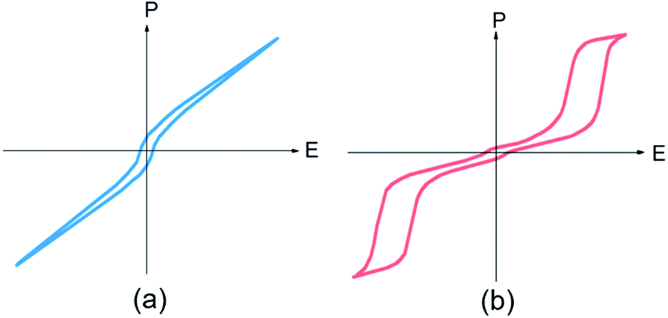 | ||
| Fig. 2 Schematic polarization–electric field hysteresis loops for AgNbO3 ceramic under (a) weak-field (≤20 kV cm−1) and (b) strong-field (≥170 kV cm−1).15,16 | ||
The discovery of “double” polarization hysteresis under strong electric fields indicated that AgNbO3 could potentially replace Pb-based antiferroelectrics in energy storage applications. Based on chemical composition adjustments, the field-induced phase transitions and the associated physical properties can be optimized. Thus, chemically-modified AgNbO3-based materials could not only meet the stringent property requirements for energy storage and energy exchange devices, but also overcome the environmental drawbacks of lead-based materials. In 2016, our research team reported that AgNbO3 ceramics show great potential in energy storage applications due to the high recoverable energy density,15 triggering increased research interest in this material. The energy storage capability in chemically-modified AgNbO3 ceramics has been subsequently improved;17 it is now triple the value first reported for the unmodified composition, and even outperforms many Pb-based antiferroelectrics.
Although a large number of research studies on AgNbO3 have been reported since its discovery in 1958, comprehensive reviews on this system are still rare. Early publications dating back about 20 years ago proposed that AgNbO3 could be useful for piezoelectric and microwave applications.18,19 Additionally, following the seminal work on semiconductor-based photocatalytic technology in 1972,20 studies have also reported that AgNbO3 exhibits attractive visible-light photocatalytic activity related to its narrow band gap (∼2.8 eV) that could be suitable for producing hydrogen and for degrading water pollutants.21 More recently, the photovoltaic properties of AgNbO3 have also been explored for potential solar cell applications.22 Therefore, it is timely to comprehensively review the past and present understanding of AgNbO3 and AgNbO3-based materials to guide future development. The scope of this article is to review the synthesis, crystalline structure, microstructure and properties of these systems. In particular, the structure–property relationships of AgNbO3-based perovskites are described and recent progress on AgNbO3-based materials for high-power energy storage and photocatalysis is extensively discussed. The review is concluded with the proposal of future research, which could further improve the understanding and boost the applications of silver niobate-based materials.
2. Silver niobate (AgNbO3)
2.1 Synthesis
In the binary phase diagram of Ag2O–Nb2O5, there are five confirmed compounds with different Ag2O![[thin space (1/6-em)]](https://www.rsc.org/images/entities/char_2009.gif) :Nb2O5 stoichiometric ratios. Besides the perovskite-structured AgNbO3 (1:1),22 the other confirmed phases are the layer-structured natrotantite Ag2Nb4O11 (1:2),23 the tungsten bronze-structured AgNb3O8 (1:3),24 and the AgNb7O18 (1:7)25 and AgNb13O33 (1:13)26,27 compounds. It has been reported that these other compounds have similar properties to AgNbO3, also exhibiting anti-/ferroelectricity and photocatalytic activity.23,25 Although these compounds can be synthesized via conventional solid-state reaction routes, it has been widely experienced that synthesizing single phase AgNbO3 in air by solid-state reaction is very difficult, due to the thermodynamic instability of Ag+ ions at elevated temperatures. To overcome this problem, the synthesis process is often carried out in an atmosphere of pure oxygen.13 The successful synthesis of AgNbO3 in pure O2 atmosphere using Ag2O and Nb2O5 as raw materials has been reported in several publications.15–20 During heating up to 200 °C, there is a slow reduction of Ag2O:28
:Nb2O5 stoichiometric ratios. Besides the perovskite-structured AgNbO3 (1:1),22 the other confirmed phases are the layer-structured natrotantite Ag2Nb4O11 (1:2),23 the tungsten bronze-structured AgNb3O8 (1:3),24 and the AgNb7O18 (1:7)25 and AgNb13O33 (1:13)26,27 compounds. It has been reported that these other compounds have similar properties to AgNbO3, also exhibiting anti-/ferroelectricity and photocatalytic activity.23,25 Although these compounds can be synthesized via conventional solid-state reaction routes, it has been widely experienced that synthesizing single phase AgNbO3 in air by solid-state reaction is very difficult, due to the thermodynamic instability of Ag+ ions at elevated temperatures. To overcome this problem, the synthesis process is often carried out in an atmosphere of pure oxygen.13 The successful synthesis of AgNbO3 in pure O2 atmosphere using Ag2O and Nb2O5 as raw materials has been reported in several publications.15–20 During heating up to 200 °C, there is a slow reduction of Ag2O:28| Ag2O → 2Ag + ½O2(↑) |
The thermogravimetric curves of metallic Ag, Ag2O and Ag2CO3 as different silver sources in the formation of AgNbO3 indicate that all these Ag precursors can react with Nb2O5, to finally form AgNbO3, as shown in Fig. 3.
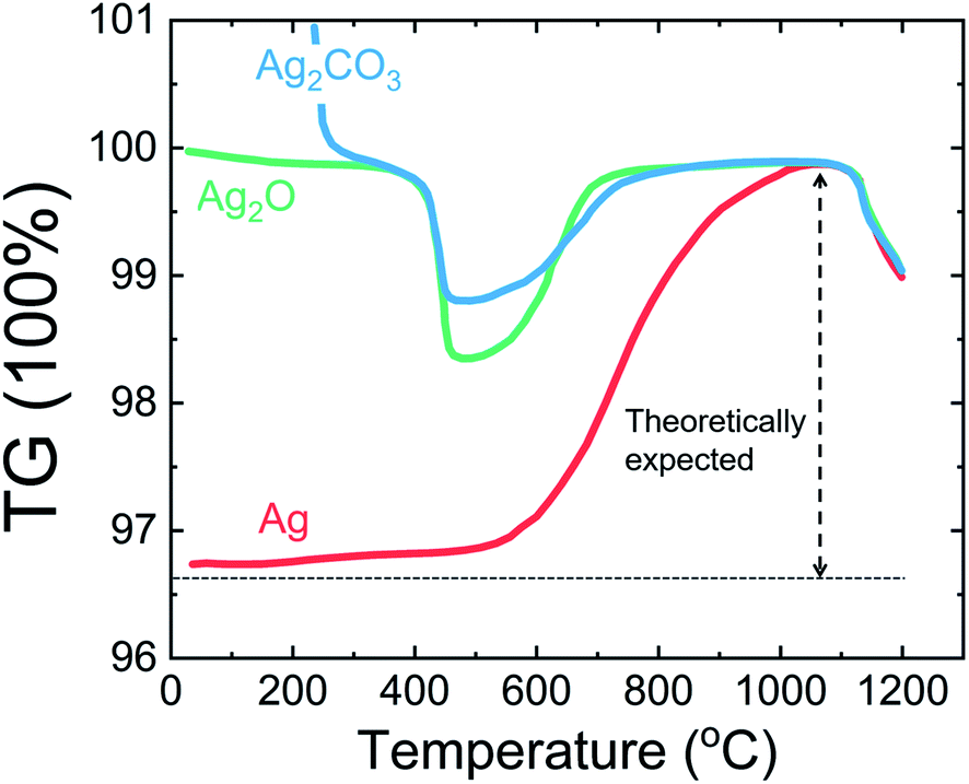 | ||
| Fig. 3 Thermogravimetric curves of mixtures of Nb2O5 with different silver sources: metallic Ag powder, Ag2O, and Ag2CO3.28 [Reprinted by permission from Springer Nature: Journal of Materials Research, copyright (2007)]. | ||
By analyzing the three curves, it can be found that Ag2O and Ag2CO3 go through a rather fast decomposition, leading to the formation of metallic Ag and O2 at ca. 450 °C. On further heating, the metallic Ag is re-oxidized and reacts with Nb2O5 to form AgNbO3 at ca. 800 °C, which melts and decomposes at ca. 1140 °C. The kinetics of the chemical reaction using metallic Ag are much slower than that using Ag2O/Ag2CO3 precursors. The temperature for the complete formation of AgNbO3 using metallic Ag is ca. 1060 °C. From Fig. 3, it is evident that only part of the Ag content is reduced in the initial stages of the reactions involving Ag2O and Ag2CO3 and that the subsequent re-oxidation stage is completed more rapidly than in the case of the reaction with pure Ag, where the oxidation of the entire Ag content is required. An alternative strategy to synthesize pure AgNbO3 without O2 atmosphere is represented by wet chemical methods. It was reported that pure AgNbO3 powders can be synthesized via hydrothermal processing at 160–240 °C using analytical grade NH4HF2, Nb2O5, and Ag2O as raw materials in an acid solution (pH = 3).29,30
Other chemical methods, such as sol–gel and co-precipitation have also been developed, using Ag and Nb alkoxides or citrates as precursors, with a firing step performed at 650 or 800 °C that burns off the organic ligands and leads to the formation of AgNbO3.31 The color of the AgNbO3 synthesized powders is usually milk-like or faint yellow, but it becomes darker, from red to gray, under visible-light.
AgNbO3 single crystals can be grown via the molten-salt method using NaCl or V2O5 as flux agents.32,33 Using flux methods, recently, Zhao et al. have successfully grown AgNbO3 single crystals using Ag2O (99.9%), Nb2O5 (99.99%), and V2O5 (99.2%) with a molar ratio of 7.4:1:4 in the starting mixture.34 Polycrystalline bulk ceramics can be obtained by sintering synthesized AgNbO3 powders at high temperature (usually from 1060 to 1120 °C) in O2 atmosphere.28,35 The prepared AgNbO3 ceramics are generally yellowish in color. It should be noted that the decomposition temperature of AgNbO3 is ca. 1120 °C, which is very close to the densification temperature of the ceramics, making the sintering of high density AgNbO3 ceramics rather challenging. Therefore, precise temperature control is essential to prepare high-quality AgNbO3 bulk ceramics. Generally, the melting or decomposition of AgNbO3 ceramics begins at the surface when the sintering temperature is too high, and leads to the appearance of impurity phases, such as Ag2Nb4O11 and AgNb3O8, amongst others. These impurities are usually confined within the surface layers and can be removed via a fine grinding process. By contrast, rough grinding would lead to the modification of the original lattice and to a number of artificial defects originating from the unstable chemical structure. Recently, it has been reported that Ag quantum-dots/nanoparticles are formed on AgNbO3 after irradiation with a Xe lamp.36 Theoretical modelling and simulations have shown that due to Ag deficiency, Schottky defect clusters consisting of two Ag vacancies and an O vacancy (i.e.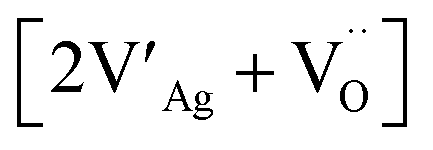 defect complex using the Kroger–Vink notation) can be formed in AgNbO3 perovskites.37 Kania et al. investigated the influence of Ag deficiency on microstructure and found that a few percent excess of Ag2O in the starting composition can significantly increase the homogeneity of the perovskite structure and can thus improve the quality of AgNbO3 ceramics.38 On the other hand, a large excess of Ag2O in the starting composition leads to the presence of metallic Ag. To avoid Ag deficiency at high temperature, Kitanaka et al. attempted to grow AgNbO3 single crystals using slow cooling and Czochralski methods in a high-pressure O2 atmosphere. They found that a high oxygen pressure can significantly prevent Ag deficiency, especially in the Czochralski method.39 The materials used in high-power energy storage systems require high electrical insulation under strong field conditions and large electrical breakdown strength (Eb). The Eb of unmodified AgNbO3 ceramics prepared by the solid-state method in pure O2 atmosphere is 200 ± 20 kV cm−1.13,15,16 The effects of Ag deficiency on electrical properties were also reported in our recent publication, where small amounts of Ag deficiency favor increased stability of the AFE state.40
Due to the demand for miniaturized electronic devices, the preparation of AgNbO3 thin films has also been explored over the past ten years, particularly for microwave applications. The two primary deposition techniques used to prepare AgNbO3 films include chemical solution deposition (CSD) and pulsed laser deposition (PLD). Telli et al. showed that AgNbO3 thin films can be grown on (001) SrRuO3/(001) LaAlO3 substrates by CSD.41 Nevertheless, thin films prepared using this method showed significantly distinct dielectric properties compared to bulk ceramics. Kim et al. reported that AgNbO3 films can be grown on LaAlO3 (001) and sapphire (Al2O3-0112, r-cut) single crystals substrates by PLD, from stoichiometric AgNbO3 ceramic targets.42 Using PLD technology,43 thin films grown on SrTiO3 (STO) single crystal substrates with different orientation can exhibit ultrahigh Eb values (∼400 kV cm−1). Furthermore, it is interesting to note that AgNbO3 films grown on (001) STO exhibited “double” polarization hysteresis, while AgNbO3 films deposited on (110) and (111) STO substrates showed a “ferroelectric-like” polarization hysteresis under strong-field cycling. However, the authors did not perform a structure investigation to clarify the reasons for this difference. More recently, Zhang et al. grew AgNbO3 epitaxial films on (001) STO substrates using the PLD method.44 The film showed double polarization hysteresis with a higher AFE–FE phase transition field and a higher Eb value (624 kV cm−1), indicating that such methodology may be viable for the fabrication of AgNbO3 with high breakdown strength.
2.2 Crystal structure
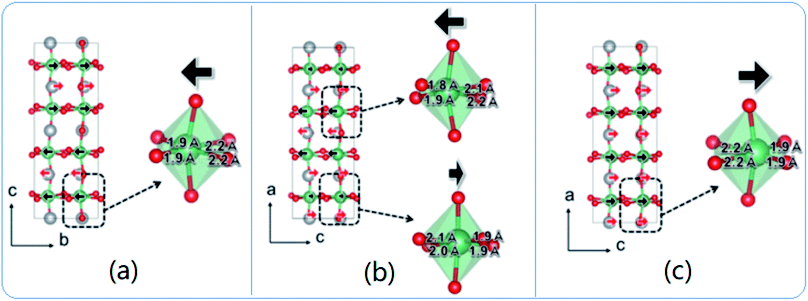
The exact crystallographic structure of AgNbO3 is still under debate. Initially, it was suggested that AgNbO3 is ferroelectric at room temperature with a tiny “ferroelectric-like” polarization observed under a weak electric field of 17 kV cm−1 (remnant polarization Pr ≈ 0.04 μC cm−2) and a low piezoelectric response (piezoelectric coefficient d33 ≈ 0.24 pC N−1).14,45 Subsequent investigations using powder diffraction techniques, including X-ray diffraction (XRD) and neutron diffraction (ND), demonstrated that AgNbO3 displays an antipolar ordering with antiparallel displacements of Ag+ and Nb5+ in the centrosymmetric space group, Pbcm,46–48 which is inconsistent with its electrical response. To resolve this ambiguity, in 2011, Yashima et al. carried out a comprehensive investigation by analyzing data generated by convergent beam electron diffraction (CBED), ND and synchrotron XRD, and suggested a weak polar or ferrielectric (FIE) structure, modelled with the non-centrosymmetric space group, Pmc21, where both Nb5+ and Ag+ cations show antipolar behavior. Since the unit-cell showed a weak net polarization, AgNbO3 was categorized as a “non-compensated AFE”, which is distinct from typical AFEs.49 In 2012, based on theoretical calculations, Niranjan et al.50 revealed the possibility that Pmc21 and Pbcm phases may coexist, as supported by the small difference between their free energies (only 0.1 meV f.u.−1).Fig. 4 shows that the refined structure models of Pmc21 and Pbcm space groups are very similar. Both structures show a structural distortion with a (a−b−c+)/(a−b−c+) tilting using Glazer's notation. Actually, distinguishing the two structures based on average structural analysis methods such as XRD and ND is very difficult, since both structural models can fit the experimental data very accurately and give satisfactory refinement results. The Pbcm space group is a super-group of Pb21m, with some classes of diffraction peaks theoretically present in the latter but systematically absent in the former.16 For Pbcm, the full Hermann–Maugin symbol is P 2/b 21/c 21/m generating systematic absences of the type k = odd for 0kl, l = odd for h0l and hence k = odd for 0k0, and l = odd for 00l reflections. For Pb21m (transformed from Pmc21 to ensure that the axial assignments are consistent with Pbcm), the center of symmetry is lost as is much of the translational symmetry leaving only the b-glide perpendicular to the a-axis and a 21 screw axis parallel to the b-axis, to generate systematic absences of the type k = odd for 0kl and k = odd for 0k0. Thus, the Pb21m structure can be distinguished by the presence of 00l or h0l reflections where l is odd. Indeed in our previous work,16 00l diffraction spots with l = odd were found in selected area electron diffraction (SAED) patterns, while further tilting experiments confirmed that these were not due to double diffraction (Fig. 5).
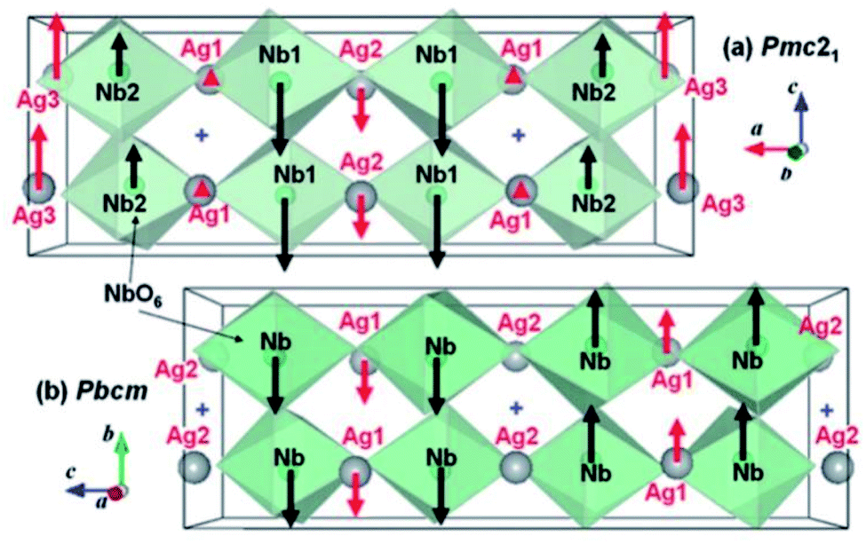 | ||
| Fig. 4 Refined structure models of non-centrosymmetric Pmc21 and centrosymmetric Pbcm phases. Red and black arrows indicate the displacements of Ag+ and Nb5+ ions, respectively, from the center of the bonded oxygen positions. The “cross” symbol indicates the center of symmetry in the Pbcm structure.49 [Reproduced with permission from ref. 49 copyright 2011 American Chemical Society]. | ||
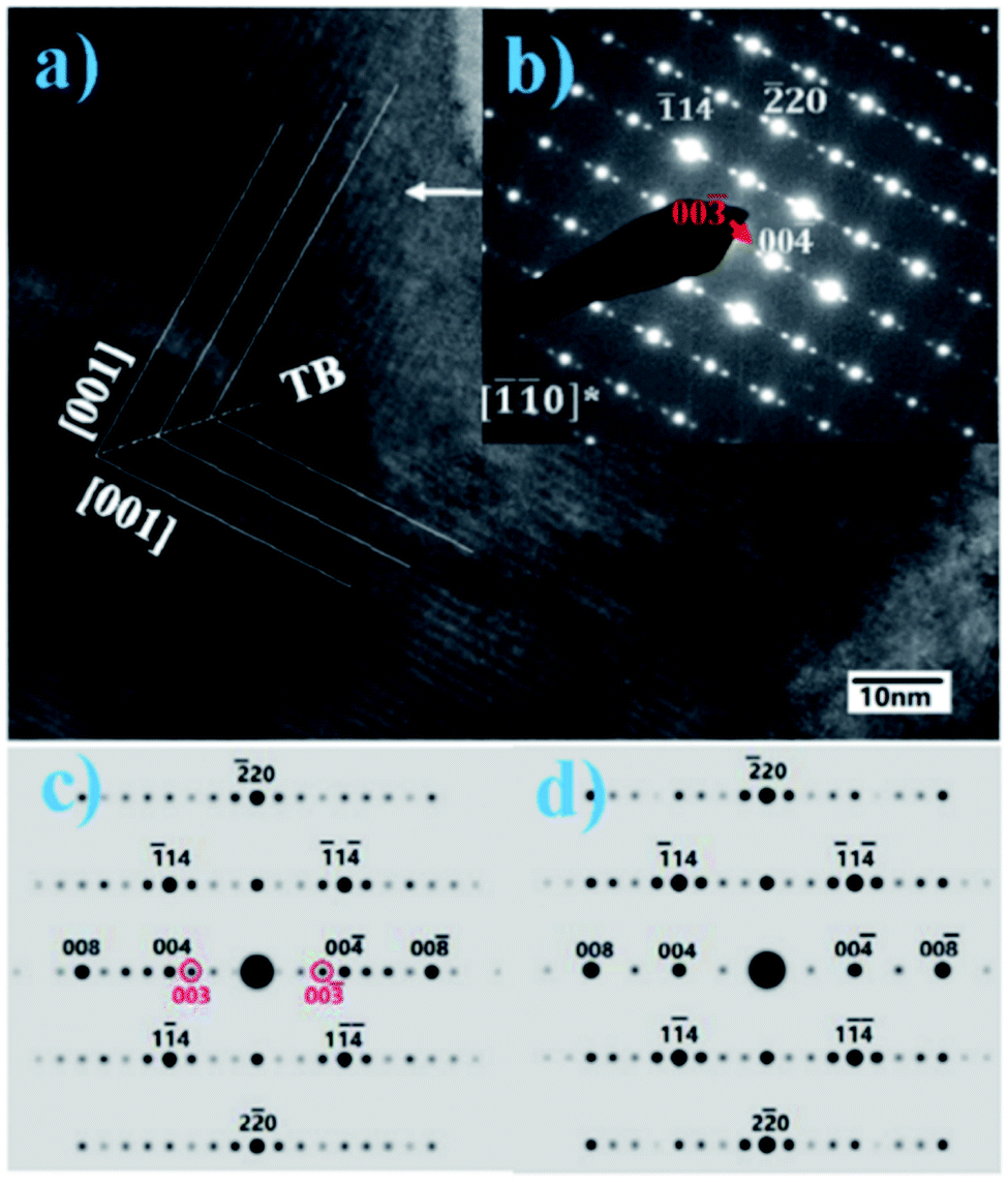 | ||
| Fig. 5 (a) HREM and (b) observed SAED pattern at the [−1−10] zone axis; (c) and (d) calculated SAED patterns of Pb21m and Pbcm space groups, respectively.16 | ||
The simulated electron diffraction (ED) patterns clearly indicate that the space group is Pb21m rather than Pbcm, consistent with the early structure investigation reported by Yashima et al.49 Using spherical aberration correction methods, Li et al. obtained high-angle annular dark-field (HAADF) images of AgNbO3, where the fast Fourier transform pattern, as well as the ED patterns, indicated that the structure tends to the non-polar Pbcm space group.51 However, more recently, using a combination of high-resolution neutron and synchrotron X-ray powder diffraction, Farid et al. reported the structure as being polar in space group P21am (related to Pb21m by axial transformation).52
Second harmonic generation (SHG) experiments can be used to identify whether or not a structure has inversion symmetry. A very weak SHG signal was found in AgNbO3 powder and ceramic samples, which disappeared on heating at around 170 °C, indicating that at least part of the structure has inversion symmetry below this temperature.16 Recently, Lu et al. systematically demonstrated the difference between the Pbcm and Pmc21 structures in terms of crystallographic symmetry.53 Each of the two distorted structures can be constructed via the coupling/competition between specific “softening” symmetry-modes within the first Brillouin-zone of the non-distorted parent structure. The scheme in Fig. 6 shows the structure distortion induced from the undistorted parent structure (Ammm) by specific symmetry-modes. The T4+ and H2 modes, located at the zone-boundary, can induce an R(〈110〉p)-type octahedral rotation (i.e., (a−a−c0) tilting) and an R(〈001〉p)-type octahedral rotation (i.e., (a0a0c−)/(a0a0c+) tilting), respectively. The Λ3 mode is mainly associated with the off-centering displacement of cations, which can result in an anti-parallel alignment of dipoles. The Γ4− mode, located at the zone-center, is an FE mode, which can induce all ions to move along a specific direction but with different magnitudes. The coupling of T4+ and H2 modes could induce a secondary Λ3 mode and finally construct the Pmca (axial transformation from Pbcm) distorted structure, while an additional “softening” of the primary mode Γ4− could lower the symmetry from Pmca to Pmc21. The global amplitude of the Γ4− mode is far from the amplitude of the Λ3 mode, which is responsible for the observed weak-ferroelectricity in AgNbO3.
 | ||
| Fig. 6 (a) and (b) Distorted AgNbO3 (AN) structure induced by the T4+ mode only, viewed along (a) the c-axis and (b) the a-axis. (c) and (d) Distorted AN structure induced by the H2 mode only, viewed along (c) the a-axis and (d) the b-axis. The +/− signs on the right in panel (d) show clockwise/anticlockwise rotations, respectively, of the right-hand column of octahedra around the a-axis. (e) The distorted structure induced by the Λ3 mode only, and (f) that of the Γ4− mode only. The black arrows in panel (e) show the off-center displacements of Nb5+ and Ag+ cations, while the red arrows in panels (e) and (f) indicate the local spontaneous polarization. The horizontal dashed red lines represent antiphase boundaries for octahedral rotation around the a-axis in panel (d), and cation displacements along the c-axis in panel (e).53 | ||
2.3 Dielectric properties and temperature-driven transitions
Besides the controversy regarding its crystallographic structure at room temperature, AgNbO3 has also been reported to display a series of temperature-induced phase transitions between different polymorphs, the details of which are still under debate. Generally, the structural transitions for non-linear dielectric materials (such as anti-/ferroelectrics) can be detected by measuring the temperature-dependence of dielectric properties and identifying the presence of dielectric anomalies that could originate from phase transitions. In 1958, Francombe et al. synthesized AgNbO3 and studied its structure and dielectric properties; the relevant results of their study are reported in Fig. 7a and b.35 In the plots, three dielectric anomalies at ca. 60, 260 and 340 °C can be observed; however, the structure analysis indicated that only the dielectric anomaly around ca. 340 °C relates to a phase transition (from orthorhombic to tetragonal structures). Furthermore, the structure analysis indicated that when the temperature approaches ca. 580 °C, a phase transition from the tetragonal to the cubic phase occurs, although no obvious dielectric anomaly can be found around this temperature (Fig. 7a). | ||
| Fig. 7 Thermal dependence of (a) permittivity and (b) lattice parameters of AgNbO3 reported by Francombe et al.;35 (c) temperature dependence of dielectric permittivity and loss of AgNbO3 reported by Kania et al.;54 [reproduced from ref. 54https://doi.org/10.1088/0953-8984/11/45/316 with permission from copyright IOP Publishing]. (d) Schematic showing the axial relationship between orthorhombic symmetry in rhombic (aR, bR, cR) and parallel orientations (ap, bp, cp), respectively (ac, bc, cc represent the axes of the pseudo-cubic unit cell). | ||
With the improvement of characterization equipment, Kania et al. re-investigated the relationship between polymorphic structure and dielectric properties and proposed the following polymorphic phase transition sequence during heating54 (Fig. 7c):

M1, M2 and M3 denote phases with orthorhombic (O) symmetry in rhombic orientation. The T and C phases have tetragonal and cubic symmetries, respectively. O1 and O2 represent phases with orthorhombic symmetry in parallel orientation. A schematic diagram of the O symmetry with different orientations is shown in Fig. 7d. The transitions between the high-temperature M3, O (O1 and O2), T and C phases are related to the thermal evolution of octahedral tilting,55,56 as observed by XRD35,55,57 and TEM56 experiments. However, no evidence of structural change can be observed in XRD or TEM for the O1 ↔ O2 transition. It should be noted that the M-type phase transitions were only ascertained via analyzing in situ diffraction data based on the primitive perovskite pseudo-cubic unit-cell using monoclinic parameters (hence their designation as “M” phases). The changes in structural parameters that distinguish the three M phases are mostly consistent with the dielectric anomalies around ca. 70 °C and ca. 270 °C. Additionally, dielectric spectroscopy also revealed a peculiar sharp anomaly at ca. 170 °C which appeared only in the cooling cycle and was hardly detected during heating, as shown in Fig. 7c. This was attributed to the dipole freezing temperature, Tf. During the 1980s, it was believed that the M1 phase was ferroelectric, while the M2 and M3 phases were antiferroelectric, and the O1, O2, T and C phases were paraelectric. With the help of neutron diffraction, the symmetries of the high-temperature phases O, T and C have been better understood and their space groups have been identified as Cmcm, P4/mbm and Pm![[3 with combining macron]](https://www.rsc.org/images/entities/char_0033_0304.gif) m, respectively.47 However, the exact symmetry of the M phases, the dielectric anomalies related to M-type phase transitions, as well as the so-called freezing temperature (Tf) are still under debate. Based on dielectric studies combined with infrared and Raman spectroscopy results reported in early publications,58–60 the dielectric anomalies have been related to the different evolutionary stages of displacive Nb5+ ion dynamics, evidenced by the presence of submillimeter relaxation modes in the dielectric spectra shown in Fig. 8a and b, and the center component (P1 peak) in Raman spectra shown in Fig. 8c.
m, respectively.47 However, the exact symmetry of the M phases, the dielectric anomalies related to M-type phase transitions, as well as the so-called freezing temperature (Tf) are still under debate. Based on dielectric studies combined with infrared and Raman spectroscopy results reported in early publications,58–60 the dielectric anomalies have been related to the different evolutionary stages of displacive Nb5+ ion dynamics, evidenced by the presence of submillimeter relaxation modes in the dielectric spectra shown in Fig. 8a and b, and the center component (P1 peak) in Raman spectra shown in Fig. 8c.
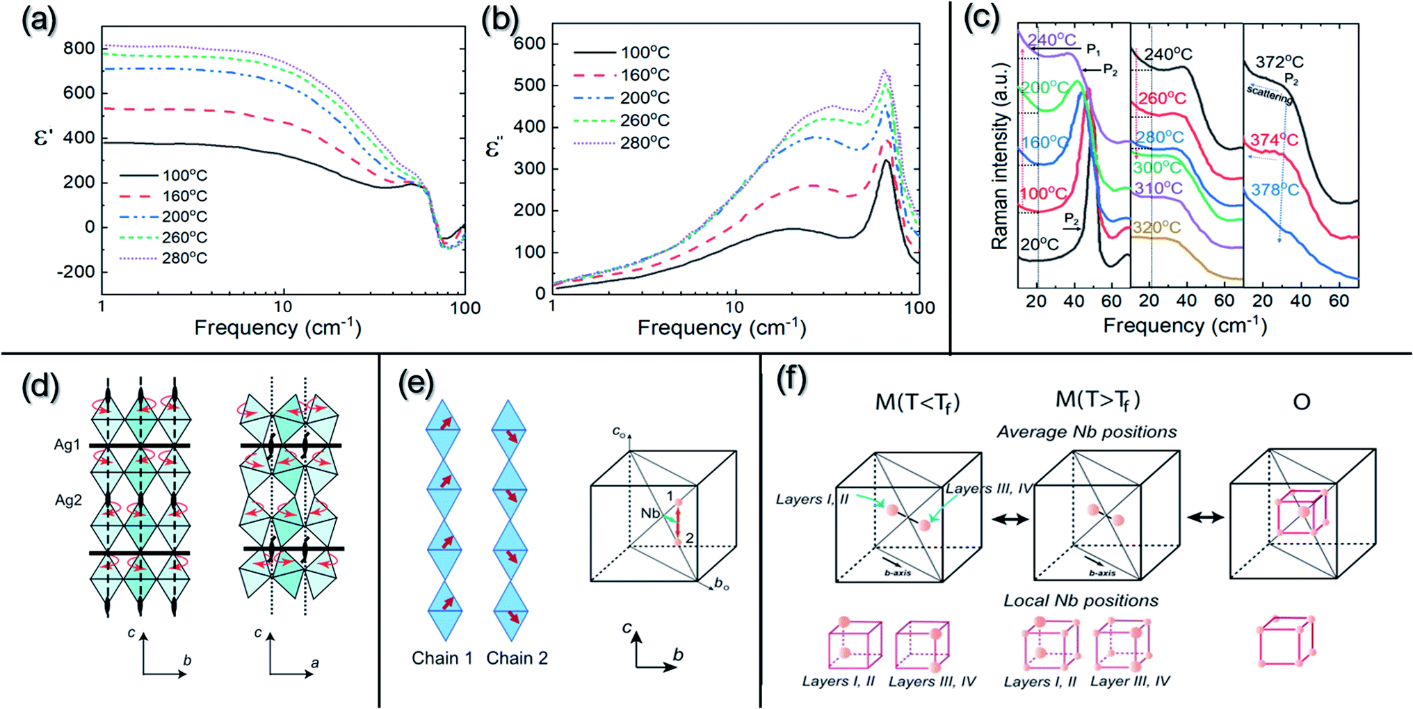 | ||
| Fig. 8 (a) Real (ε') and (b) imaginary (ε′′) parts of the dielectric permittivity as functions of temperature for AgNbO3 in the 1–100 cm−1 frequency range (data as reported by Fortin et al.)60 reproduced from ref. 60https://doi.org/10.1063/1.361796 with the permission of AIP Publishing; (c) temperature dependence of the low-frequency Raman spectra of AgNbO3 (data as reported by Kania et al.)61 reproduced from ref. 61https://doi.org/10.1088/0022-3719/19/1/007 with permission from copyright IOP Publishing (note: only Stokes Raman scattering is re-plotted in (c)). The spectra show an intense low-frequency phonon peak (P2) and a strong central component (P1), the intensity of which clearly rises with temperature and reaches a maximum at around 240 °C (corresponding to the M2–M3 transition). The phonon peak (P2) shifts to lower frequency with increasing temperature and abruptly disappears around 378 °C (corresponding to the O–T transition). The diffuse peak, P1, above 320 °C, is caused by the scattering of the initial phonon peak; (d) schematic of the octahedral framework within the non-polar Pbcm symmetry of AgNbO3, in which octahedral rotations about the c-axis are indicated using arrows, while Ag1 and Ag2 specify c-planes occupied by the symmetrically non-equivalent Ag cations; (e) (left) schematic of the chain-like correlations for the local Nb displacements directed along [111]c and [11–1]c directions; (e) (right) a random mixture of chains 1 and 2 equivalent to average Nb displacements along the [110]c direction (i.e., b-axis of orthorhombic crystal); (f) schematic for the Nb5+ displacive order–disorder behavior as a function of temperature.48 [Reprinted with permission from ref. 48https://doi.org/10.1103/PhysRevB.79.104113 copyright 2003 by the American Physical Society]. | ||
These connections have been further explored in a systematic structure investigation reported by Levin et al. in 2009.48 Based on various techniques that allow for probing of the local structure, such as neutron pair distribution functions (PDFs) and extended X-ray absorption fine structure (EXAFS), local structural distortions upon heating were detected and correlated to the order–disorder behavior of displacive Nb5+ cations in the octahedral framework of the non-polar Pbcm matrix. The octahedral framework in the Pbcm symmetry of AgNbO3 observed from the c–b and c–a planes is shown in Fig. 8d, in which a sequence of two in-phase and two antiphase octahedral rotations about the c-axis yields a 4ac periodicity with two crystallographically distinct Ag sites. The chain-like correlation for the local off-centering Nb displacements within two adjacent octahedral columns directed along [111]c and [11–1]c can give rise to the average Nb displacements along the [110]c direction (i.e., the b-axis of the orthorhombic Pbcm structure) as shown in Fig. 8e. At high temperature, the Nb5+ cations are randomly displaced among eight sites along the 〈111〉c directions, which give the ideal positions on average in the O phase. Upon cooling, the off-centered ordered arrays of Nb5+ cations displacement along the [111]c and [11–1]c directions in two adjacent octahedral layers gives an average displacement component along the [110]c direction (i.e., along the b-axis of the orthorhombic Pbcm structure). In the two next adjacent layers, these average displacement components point in opposite directions, leading to AFE structural order. Locally, Nb5+ cations still occupy these eight positions, but two of these locations are preferred. Upon further cooling, the occupancy probabilities for the remaining six sites decrease and vanish below Tf, leading to a partial long-range ordered antipolar-like array of Nb5+ cations and to the observed sharp dielectric response at Tf. Miga et al.62 suggested that further freezing of the displacive Nb5+ and Ag+ sites on sub-lattice scales could lead to a weakly-polar relaxor ferroelectric or dipolar glass transition corresponding to the M1 ↔ M2 transition. Such disorder–order behavior of displacive cations has been used to successfully explain the polymorphic ferroelectric transitions in KNbO3 and BaTiO3, as reported in early studies.63–65 In these cases, due to the absence of octahedral tilting, the partial ordering of off-center Nb5+/Ti4+ displacements, on cooling, triggers a sequence of well-defined thermodynamic phase transitions accompanied by changes in symmetry (i.e., tetragonal → orthorhombic → rhombohedral).
It should be noted that the local structural distortions that induce the dielectric anomalies separating the M-type polymorphs of AgNbO3 suggested by Levin et al.48 are based on the lattice matrix with Pbcm symmetry. However, in 1983, Kania et al. reported that the weak ferroelectricity in AgNbO3 disappeared during heating at ca. 70 °C.14 After discovering this weak ferroelectricity, researchers preferred to link the M1↔ M2 phase transition to a structural change between the Pmc21 and Pbcm symmetries. This phase transition should be accompanied by a soft mode at the first Brillouin zone center, but Raman scattering does not offer any evidence for such an effect near ∼70 °C (see Fig. 8c). Instead, the central component corresponding to P1 in Fig. 8c presents more obvious changes as a function of temperature and it progressively disappears approaching ca. 300 °C (in the M3 region). This feature is closely related to the Nb5+-ion dynamics. In other words, the M1 ↔ M2 phase transition is possibly related to local structural variations or to an improper ferroelectric transition as defined by Dvorak (i.e., the primary driving force inducing this transition is not the polarization order parameter).66 Based on in situ high-energy X-ray diffraction studies, Yoneda et al. provided additional insights into the temperature-driven polymorphic nature of the so-called M-phases.67 In this study, the authors found that the Ag+ ion shows displacive disorder behavior. This discovery indicated the existence of an intricate coupling between octahedral tilting and local displacements of Ag+ ions since the octahedral tilting can usually lead to the off-centering of A-site cations within the AO12 cage of the perovskite structure. The authors suggested that these interactions trigger a series of changes in the cation displacements across the so-called M phases, being similar to the situation in Pb-based solid-solutions near the morphotropic phase boundary (MPB). In Pb-based perovskites, three kinds of monoclinic phases (MA, MB, and MC) can be formed due to the displacive ordering of cations shifting along specific directions (i.e., polarization rotation) from the parent tetragonal phase, as shown in Fig. 9.68 Considering PbZr0.48Ti0.52O3 as an example, the monoclinic structure can be derived from the tetragonal structure by shifting the Pb and Zr/Ti cations along the tetragonal [101] axis. The monoclinic phase in Pb-based solid-solutions provides a bridge between the ground states of rhombohedral and tetragonal structures.
 | ||
| Fig. 9 Direction of the spontaneous polarization in the three types of monoclinic phases with the usual nomenclature MA, MB (Cm) and MC (Pm) redrawn, according to ref. 68. | ||
However, early ND studies on AgNbO3 provided no evidence for a ground state with rhombohedral symmetry, even at low temperatures down to 1.5 K.47 Nevertheless, a ground state rhombohedral phase can be found in (Ag0.94Li0.06)NbO3, which suggests that a rhombohedral-like structure may be buried in the local disorder of Ag atoms of the undoped AgNbO3.69 In 2014, Zhang et al.70 reported the occurrence of an additional dielectric anomaly in the low-frequency range around 250 K in AgNbO3 ceramics related to a first-order phase transition (denoted as M0 ↔ M1), as also supported by the presence of sharp anomalies in the differential scanning calorimetry (DSC) thermogram (see ref. 70, and Fig. 4 and 5). It should be noted that this ceramic was prepared using an AgNbO3 powder synthesized by a hydrothermal method.71 Kania et al. carefully re-measured the DSC and dielectric properties of AgNbO3 ceramics and single crystals, and found results to be consistent with previous investigations with no additional events found around 250 K in the dielectric and thermal data.72 Kania et al.72 argued that the extra dielectric anomaly reported by Zhang et al.70 is more likely to originate from the increasing electrical conductivity around 250 K rather than an intrinsic dielectric process of AgNbO3, indicating that water contamination is not negligible and that its prevention is necessary during experiments to avoid misinterpretation. Recently, our research team compared the variation of the temperature-dependent properties of unpoled samples including dielectric, DSC, dynamic mechanical analysis (DMA), as well as SHG data as shown in Fig. 10.16 It was found that the dielectric anomaly at the freezing temperature Tf (see Fig. 7c),52 also appeared in the dielectric data on heating, suggesting that this dielectric anomaly might be related to a temperature-driven reversible transition.
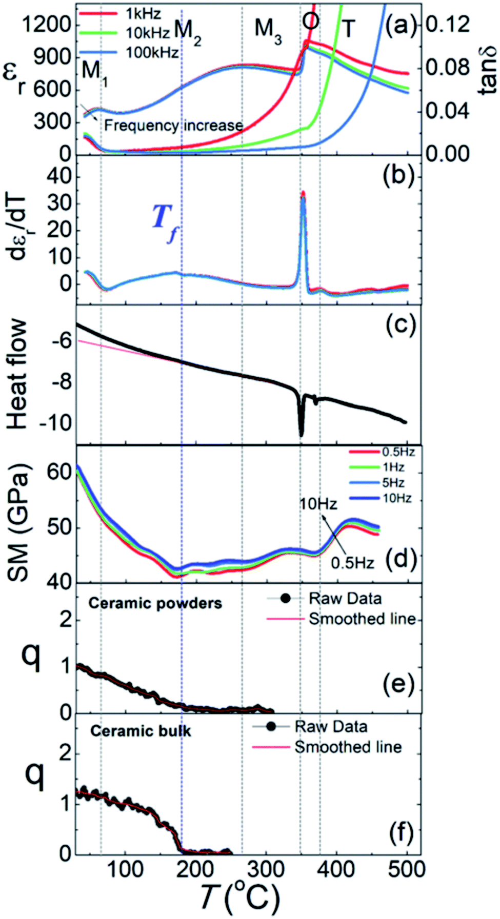 | ||
| Fig. 10 Thermal dependencies of (a) relative dielectric permittivity (εr) and dielectric loss tangent (tanδ) at selected frequencies, (b) dεr/dT, (c) DSC thermogram, (d) storage modulus (SM); (e) SHG for ceramic powders and (f) SHG for bulk ceramics (note: q = I2w/I2w (SiO2)) of AgNbO3. All plots were generated during heating.16 | ||
The comprehensive analysis of the properties shown in Fig. 10 indicated that the dielectric anomaly at “Tf” might not be associated with the freezing of Nb-ion dynamics, but could rather be ascribed to a second-order structural transition related to the breaking of inversion symmetry (i.e., Pmc21 ↔ Pbcm). It is possible that the primary driving force of this transition is the spontaneous strain rather than the spontaneous polarization (i.e., an improper ferroelectric transition),66,73 since a significant change in the storage modulus can be found at Tf (see Fig. 10d). Additionally, the dielectric behavior under a DC bias field is very similar to that of typical relaxor-ferroelectrics, such as PbMg1/3Nb2/3O3 (see ref. 16, Fig. 7). It could be reasonably deduced that the M1 ↔ M2 and M2 ↔ M3 transitions are related to local structural distortion in the polar (Pmc21) and non-polar (Pbcm) phases, respectively. In particular, the diffuse dielectric anomaly associated with the M2 ↔ M3 transition can be intimately related to disorder–order behavior of displacive Nb5+ dynamics on the sub-lattice scale in the non-polar Pbcm structure matrix. Recently, by studying Ag1−3xBixNb0.8Ta0.2O3 ceramics, Yan et al. found that within the M2 phase stability region, two structural characteristics can be identified, and were denoted as the M2a phase (at T < Tf) and the M2b phase (at T > Tf). The M2a phase is polar non-centrosymmetric, while M2b is centrosymmetric. Moreover, they also proposed that even in the M3 region, a few polar regions still persist, as evidenced by the observed weak satellite spot assigned to the (003) reflection of the Pb21m structure.74 Additionally, Gao et al. investigated the local structural features, including interatomic distance distributions and atomic displacements, using neutron small-box pair distribution function (PDF) refinement in conjunction with large-box reverse Monte Carlo modelling, and found that at room temperature (300 K), with increasing the sizes of small-box PDF refinement, the structure tends to be non-polar, while at high temperature (T > Tf, e.g. 500 K), the non-polar structure provides a better description, regardless of the size of the PDF refinement. The results of this study further support the difference between the structure below and above Tf, and indicate that the dielectric anomaly assigned as Tf, originates from a phase transition.75 Most recently, after analyzing the local structure data obtained from spherical aberration-corrected STEM, Li et al. suggested that at room temperature, besides the off-centering of Nb5+ ions along ±[110]c forming AFE Pbcm or FIE Pmc21 structures, the deviation of Nb5+ ions along ±[001]c directions was also found in local regions. They further point out that these local off-centering cations form polar nanoregions (PNRs), which are responsible for the observed relaxor dielectric response assigned to the M1 ↔ M2 phase transition. Their results further support the idea that the so-called M1 ↔ M2 transition is more likely related to a local structural evolution.76
2.4 Ferroelectric properties and field-induced transitions
The earliest proofs of ferroelectricity in AgNbO3 were based on the observation of non-linear and hysteretic P–E loops under a weak-field (<20 kV cm−1)14,45 that displayed a very small remnant polarization. In 2007, based on high quality AgNbO3 ceramic samples, Fu et al.13 observed a “double” polarization hysteresis under high electric fields (see Fig. 11). The different polarization behavior under weak-field and strong-field conditions suggested that the virgin structure undergoes at least two types of field-induced processes, involving FE domain switching and a field-induced phase transition. In other words, the virgin structure should contain either FE or AFE states. To explain the peculiar polarization hysteresis observed in the experiments, Yashima et al.49 suggested an FIE (i.e. “non-compensated AFE”) Pmc21 structure after studying diffraction data including CBED, ND and synchrotron XRD data. Furthermore, Moriwake et al. carried out molecular dynamics simulations on monocrystalline AgNbO3, and proposed that polarization switching or a field-induced transition occurs at temperatures around −73 °C and above. Regardless of whether the simulations commenced from the AFE Pbcm or FE Pmc21 structures, above −73 °C the crystal fluctuates between the two forms.77 | ||
| Fig. 11 Electric displacement vs. electric field loops measured under (a) a maximum applied field of 220 kV cm−1, and (b) a maximum applied field of 80 kV cm−1.13 [Reproduced from ref. 13https://doi.org/10.1063/1.2751136 with the permission of AIP Publishing]. | ||
However, detailed studies of polarization–current–electric field hysteresis loops reported by Tian et al.15,16 revealed more complicated electric-field-induced polarization events taking place in AgNbO3 ceramics, providing further insights into the virgin structure and electric field-induced transformations, as well as on the temperature dependence of the polymorphic nature of AgNbO3 perovskites. At room temperature, a ferroelectric-like polarization hysteresis with weak remnant polarization can be observed upon applying an alternating electric field of 60 kV cm−1 (Fig. 12a), being similar to that reported in early studies. The I–E loops revealed two current peaks (denoted as P1 and P2) located at 6 and 30 kV cm−1, respectively, which represent two kinds of field-induced polarization events.
 | ||
| Fig. 12 (a) P–E and I–E loops for AgNbO3 with successive cycles under a maximum applied field of ±60 kV cm−1 and a frequency of 10 Hz; (b) I–E data generated in the initial 1st and 2nd semi-cycles; thermal dependence of the current peaks on (c) heating and (d) cooling.15,16 | ||
The data recorded in the first-poling cycle shown in Fig. 12b clearly reveal a sharp current peak, +P1, around 6 kV cm−1. The peak +P2 located at higher electric field is not clearly visible in the first poling cycle, but careful observation reveals a small step around 30 kV cm−1. Further insights into the origin of these current peaks were obtained by their temperature-dependence shown in Fig. 12c and d, which confirmed that the current peaks P1 and P2 disappeared around the temperatures associated with the M1 ↔ M2 transition and Tf, respectively. Similar features have been observed in the I–E curves of Ag(Nb0.8Ta0.2)O3 ceramics shown in Fig. 13a.78 In the same study, a sharp dielectric anomaly, assigned to Tf, was clearly observed during heating, in contrast to the case of pure AgNbO3. Linear fitting of the reciprocal of permittivity using the Curie–Weiss law gave T0 = 80 °C, which is very close to the value of Tf (∼75 °C) (see Fig. 13b).
 | ||
| Fig. 13 (a) Detail of the I–E curves for Ag(Nb0.8Ta0.2)O3 ceramics at 10 Hz under an applied field of 8 MV m−1 at different temperatures; (b) temperature-dependence of reciprocal relative permittivity (1/εr) for unpoled Ag(Nb0.8Ta0.2)O3 ceramics measured at 1 MHz.78 | ||
Based on these observations and the data discussed in Section 2.3, the following possible phase scenario can be derived. The phase M1 would include the presence of polar and weakly-polar domains, both belonging to the Pmc21 symmetry. In other words, the virgin microstructure would include two kinds of polar domains with different electric dipole arrangement types in the same Pmc21 symmetry, which can be regarded as polar ferroelectric and polar ferrielectric (i.e., a non-compensated antiferroelectric). This suggestion is also supported by the simulations carried out by Moriwake et al.,77 which indicated that the polar ferrielectric phase has the same space group, Pmc21, as the polar phase, but it is characterized by a slightly different ion arrangement that makes its distinction difficult in microscopy and diffraction techniques. Fig. 14(a)–(c) further illustrate the ordering of electric dipole arrangements resulting in AFE Pbcm, FIE Pmc21 and FE Pmc21 structures, respectively.77 Most recently, domain structure observation on AgNbO3 single crystals, has also revealed the existence of polar domains, which would further support the deduction.79
 | ||
| Fig. 14 Comparison of crystal structures of (a) Pbcm (antiferroelectric), (b) Pmc21 (ferrielectric/weakly-polar), and (c) Pmc21 (ferroelectric) phases of AgNbO3. The arrows indicate the relative magnitude and direction of atom displacement contributing to the ferroelectricity (or lack thereof) in each structure.77 [Reprinted with permission from ref. 77https://doi.org/10.1103/PhysRevB.97.224104 copyright 2003 by the American Physical Society]. | ||
In this structural context, the current peak P1 corresponds to the switching of the polar domains in non-centrosymmetric Pmc21 symmetry. This switching event is no longer present above the M1 ↔ M2 transition temperature, suggesting that these polar domains are not switchable in the M2 phase region. It is noted that the size of polar domains should be nanometric and only emerge on local scales as supported by recent results based on STEM investigation.76 The current peak P2 could be related to the presence of weakly-polar domains, which are further stabilized by the applied field, as suggested by the sharpening of the peak P2 after the first cycle. This peak disappears above Tf, suggesting that these domains do not switch in the M2b centrosymmetric phase, in agreement with the loss of inversion symmetry and the closeness of Tf and the Curie–Weiss temperature. The absence of the peak P2 in the M2b phase offers further support to the idea that the Tf might be identified with the Curie point (TC) of the weakly-polar phase.
Under strong-field conditions, a “double” polarization hysteresis loop is generated (Fig. 15a), which is consistent with the results reported by Fu et al.13 In the I–E loops, six current peaks can be observed; these are different from those observed in Pb-based AFEs like PbZrO3, which only show four current peaks representing reversible phase transitions.1 The peaks denoted as EF and EB correspond to the forward field-induced transition during loading and the backward transition during unloading, respectively. The polarization induced during loading achieves a value of about 40 μC cm−2, while the remnant polarization is about 4 μC cm−2, which is much higher than the Pr in the low-field loops. This means that the sample is left with a sizable remnant polarization, which is only recovered by reversing the applied field, in correspondence to the extra current peaks ±P near ±50 kV cm−1 (denoted as key fields ±EU). It is interesting to observe that the peak P at key field EU is absent during the first poling cycle (see Fig. 15b), confirming that these additional current peaks ±P should originate from the polarization reversal of the residual strong-field-induced FE state. Interestingly, after strong-field poling of virgin sample, the authors found that the current peak P2 in the I–E loop under weak field conditions becomes stronger.15,16 This indicates that the weakly-polar phase leading to the sharp dielectric response (Tf) is metastable, and can be modified by the strong electric field. At the moment, the mechanisms of the field-induced transitions at EF are still unclear and the nature of the high field-induced structure is unknown. Based on the structural model discussed above, the transition at EF might involve the weakly-polar ferrielectric phase, as well as the non-polar antiferroelectric phase that would both transform to a polar FE phase, the former irreversibly, leading to a larger Pr and the latter reversibly, recovering at EB. However, the first-principles calculations reported by Moriwake et al.,80 indicated that a complete transition from an antiparallel alignment of electric dipoles in the non-polar Pbcm structure to the parallel alignment in the FE Pmc21 phase would require an ultrahigh electric field of 9 MV cm−1 (see Fig. 14c). Thus, the double polarization hysteresis observed in pure AgNbO3 is unlikely to originate from a typical AFE ↔ FE transition, but from a metastable weakly-polar FIE ↔ FE transition, which is not fully reversible, as suggested by the increased remnant polarization after high field cycling. The metastable FIE structure represents an intermediate state arising from the competition between the AFE Pbcm and FE Pmc21 phases. Additionally, the simulations by Moriwake et al. indicated that the field-induced FE phase and the weakly-polar/FIE phase have the same space group, Pmc21 (see Fig. 14). However, this deduction is only based on known data reported in the literature. To date, there are no experimental studies on the structure of the strong-field-induced FE phase.
 | ||
| Fig. 15 (a) Polarization–current–field hysteresis loops for AgNbO3 with successive cycles under a maximum applied field of ±180 kV cm−1 at a frequency of 10 Hz; (b) current–field loops generated in the initial 1st and 2nd cycles;16 (c) calculated P–E hysteresis loop for AgNbO3 induced by an irreversible phase transition from AFE Pbcm to FE Pmc21 phases.80 [Reproduced from ref. 80https://doi.org/10.1063/1.4941319 with the permission of AIP Publishing]. | ||
2.5 Photocatalytic, photoelectrochemical and photovoltaic properties
Besides showing anti-/ferroelectric behavior, AgNbO3 perovskites are semiconductors possessing a narrow band gap, which ranges from 2.08 to 2.93 eV (determined from UV-vis diffuse reflectance spectra).81 Initially, AgNbO3 was reported to be a visible-light-driven photocatalyst possessing the ability to obtain H2 or O2 from water in the presence of sacrificial reagents. Table 1 lists the photocatalytic activity of AgNbO3 reported by Kato et al. under various conditions.21 In particular, the photocatalytic activity of AgNbO3 was found to increase on the addition of an excess amount of Ag during preparation (i.e., Ag/Nb > 1) as shown in Table 1. Recently, a series of AgNbO3-based photocatalysts, including solid-solutions, composites and heterojunctions, have been developed for water purification and will be discussed in Section 5.3.| Catalyst | Ag/Nb ratioa | Incident light/nm | Reaction conditions | Activity/μmol h−1 | |
|---|---|---|---|---|---|
| H2 | O2 | ||||
| a In the starting materials. b Pressures of H2O and CH3OH were 20 and 70 torr, respectively. Catalyst: 0.3 g for liquid-phase reactions and 1.0 g for gas-phase reactions; reactant solution: 150 mL, 300 W Xe lamp, top window cell made of Pyrex. | |||||
| AgNbO3 | 1.00 | >420 | 0.05 M AgNO3(aq) | — | 14 |
| AgNbO3 | 1.00 | >300 | 0.05 M AgNO3(aq) | — | 119 |
| AgNbO3 | 1.05 | >420 | 0.05 M AgNO3(aq) | — | 37.0 |
| AgNbO3 | 1.05 | >300 | 0.05 M AgNO3(aq) | — | 240 |
| AgNbO3 | 1.05 | >420 | H2O, CH3OH vaporb | 1.7 | |
Electronic structure studies based on the plane-wave-based density functional method have revealed that the narrow band gap is due to the fact that the top of the valence band mainly consists of a hybrid orbital of Ag 4d and O 2p. To further understand the photocatalytic activity of AgNbO3, Li et al. investigated the surface photoelectric properties of Ag/AgNbO3 photocatalysts and suggested that the two peaks at ∼375 nm and ∼420 nm in the surface photovoltage spectrum (SPS) (see Fig. 16) are associated with two electronic transitions.82 One could correspond to the transition from O 2p to Nb 4d, being related to the UV light absorption property, and the other (∼420 nm, located at a shorter wavelength than the light absorption edge) related to visible-light absorption property was proposed to correspond to an electronic transition from Ag 4d to Nb 4d. In particular, the electric field-induced surface photovoltage spectrum (EFISPS) suggested that the second SPS peak (at∼ 420 nm related to the transition from Ag 4d to Nb 4d), determining the visible light absorption, could be enhanced or completely restrained under positive and negative external voltages, respectively, indicating tunable visible-light photocatalytic activity.
 | ||
| Fig. 16 (a) SPS of Ag/AgNbO3 with different Ag contents without an external bias. The inset shows the variations in photovoltage and wavelength of the peak in the visible light region with Ag content. (b) EFISPS of Ag/AgNbO3 (10%) at different external voltages. (c) SPS of Ag/AgNbO3 (10%) at different external voltages. (d) Schematic band structure under different biases.82 [Reproduced from ref. 82https://doi.org/10.1088/0022-3727/42/23/235503 with permission from copyright IOP Publishing]. | ||
In 2014, Zhou et al.83 revealed that AgNbO3 exhibits surface plasmon resonance (SPR) under visible light. Surface plasmons (SPs) can exist on the surface of noble metals or narrow band gap semiconductors with abundant active current carriers.84 This indicates that AgNbO3 can absorb extra visible light with wavelengths ranging from 450 to 700 nm giving it huge potential in light-harvesting technologies. The SPR was suggested to originate from weakly bound Ag atoms in the perovskite structure, favoring a metal-like state of silver ions and self-assembled microstructures of AgNbO3. The different absorptions were divided into two parts as shown in the inset of Fig. 17.83 The electron-density map and the partial density of states of AgNbO3 reported in earlier studies by Yashima et al.81 reveal a large valence band width (∼6 eV). The latter is due to the existence of Ag atoms and Ag–O and Nb–O covalent bonds, which lead to a narrower band gap (∼1.83 eV) compared to the experimental values reported in early studies, and a visible-light response. The metal-like characteristics and these transmission paths play a key role in promoting hot-electron generation and transmission.
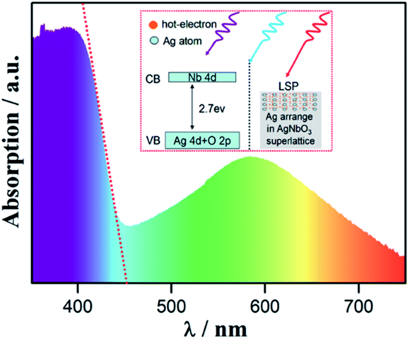 | ||
| Fig. 17 Ultraviolet-visible diffuse reflectance spectrum of AgNbO3 samples. The red dashed line is the tangential line of the eigen-absorption band side, showing the location of the band gap. Inset: schematic showing two kinds of absorption mechanism.83 [Reproduced from ref. 83https://doi.org/10.1063/1.4903912 with the permission of AIP Publishing]. | ||
Recently, Lu et al.36 discovered that Ag nanoparticles with a size of 10 nm can be grown in situ on AgNbO3 using illumination by Xe lamps, yielding a color change from yellow to brown, as shown in Fig. 18a. A change in color under light illumination was also found in our AgNbO3 fresh powders. Fig. 18c shows SEM images taken after different irradiation times. Increasing numbers of nanoparticles can be observed on the surface of grains with increasing irradiation time. These Ag nanoparticles appearing on the surface of AgNbO3 grains bring an extra absorption in the visible-light range as shown in Fig. 18b, which can be attributed to the SPR effect of Ag metal, as proposed by Zhou et al.83 Thus, the SPR effect is responsible for the enhanced photocatalytic activity at increased ratios of Ag to Nb, as shown in Table 1. The appearance of such Ag nanoparticles would lead to the creation of Ag+ vacancies in the AgNbO3 surface layers and be consistent with the theoretical prediction of Schottky defects in AgNbO3.37
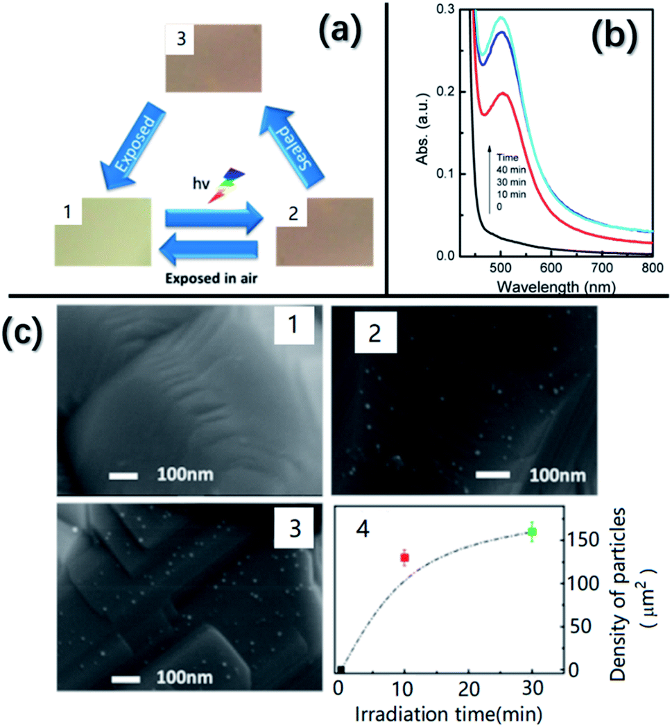 | ||
| Fig. 18 (a) Color of AgNbO3 samples in different states: (1) initial, (2) after irradiation, and (3) isolated from air and kept in the dark for 48 h. (b) UV-vis spectra of AgNbO3 irradiated with a Xe lamp for different times. (c) SEM images obtained from the samples in different states: (1) initial, (2) after 10 min of irradiation, and (3) after 30 min of irradiation. (4) Plot of density of nanoparticles versus irradiation time.36 Reprinted with permission from ref. 36https://doi.org/10.1021/acs.jpcc.6b10961 copyright 2016 by the American Chemical Society. | ||
Bulk samples of AgNbO3 have recently been reported to exhibit linear and symmetric current–voltage (I–V) curves under dark and illuminated conditions.22 In particular, the extremely weak dark conductivity (in absence of illumination) can be significantly improved by illumination. Further analysis shows that the photocurrent under a certain bias voltage increases linearly with increasing light intensity (see Fig. 19a). The UV-vis absorption spectrum shown in Fig. 19b reveals obvious absorption in the visible-light wavelength range up to 800 nm, where a weak photoelectric response (compared to the UV-light region) can be noticed up to 550 nm. The authors of the study linked the photoelectric response in the visible-light region to the presence of defects rather than to the SPR behavior mentioned above.22 The time evolution of the photocurrent response under intermittent on/off illumination shown in Fig. 19c reveals very stable photocurrent values over 1.7 nA under 10 V bias, and a large on/off ratio of 1250. The transient photocurrent curves obtained under the illumination of a nanosecond pulse laser with an emission wavelength of 355 nm (see Fig. 19d) show an instantaneous photoresponse speed of 4.7 ns and highlight the great potential for quick-response optical sensing and detection applications.
 | ||
| Fig. 19 (a) Light intensity dependence of photocurrent under a 10 V bias on illumination with a 405 nm laser. (b) UV-vis absorption spectrum and photocurrent as a function of wavelength with a 10 V bias and light intensity of 150 mW cm−2. (c) Variation of photocurrent with time on intermittent on/off illumination (405 nm laser and white light) under a 10 V bias and a constant light intensity of 150 mW cm−2. (d) Transient photocurrent curves under the illumination of a nanosecond pulse laser with an emission wavelength of 355 nm, on tripling the frequency and a pulse duration of 3–4 ns.22 [Reproduced with permission from ref. 22 copyright 2019 by John Wiley and Sons]. | ||
AgNbO3 ceramics have been also reported to exhibit a sizeable photovoltaic (PV) effect after electrical poling or mechanical polishing,22 evidenced by a non-zero short-circuit current, Isc, and open-circuit voltage, Voc, as shown in Fig. 20. However, the poling-induced PV response disappeared when the annealing temperature approached 200 °C, where no polarization switching phenomenon is observed in the I–E loop, as discussed in Section 2.4. This suggests that the PV response upon poling should be intimately related to the ferrielectric polarization. In contrast to the poling-induced PV effect, the mechanical polishing-induced PV response still persists after annealing the sample at 400 °C, which suggests that ferroelastic domains still exist at 400 °C, as reported in early studies on the domain structure.56,57 The authors suggested that the flexoelectricity induced by strain gradients could be responsible for the polishing-induced PV effects, which lead to complex spatial strain gradients distributed along the scratches.
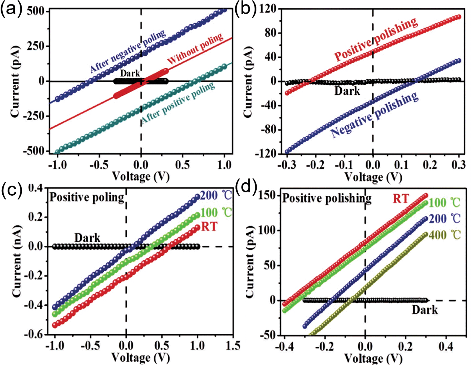 | ||
| Fig. 20 I–V curves of AgNbO3 ceramic samples prepared using different (a) poling and (b) polishing conditions. I–V curves collected under dark and illuminated (405 nm laser, 200 mW cm−2) conditions at room temperature after annealing the (c) positively poled and (d) positively polished AgNbO3 ceramic at different temperatures for 1 h.22 [Reproduced with permission from ref. 22 copyright 2019 by John Wiley and Sons]. | ||
3. AgNbO3-based solid-solutions
3.1 Anti-/ferroelectricity in perovskite oxides
Chemical modification represents a widely applied strategy to obtain specific physical properties for different applications. Based on the physical properties discovered in AgNbO3 perovskites, a number of AgNbO3-based materials have been explored; in particular, some AgNbO3-based solid-solutions were found to hold great potential for microwave applications, as well as for dielectric capacitors and piezoelectric, pyroelectric and high-power energy storage devices.The structure of the ideal ABO3 cubic perovskite can be described as being based on a cubic close packed array of oxide ions with ¼ of these replaced by A cations. The B cations are located in ¼ of the octahedral interstices. Generally, the occurrence of anti-/ferroelectricity in perovskite structures is caused by the slight distortion from the high-temperature cubic phase. There is an important question to be clarified: why does a distorted structure form in some perovskite-structured compounds during cooling? Especially for AgNbO3, the structural distortion is highly complex. It is well known that the stability of the perovskite structure (see Fig. 21) can be linked to its geometry by the tolerance factor (t) as discussed by Bartel et al.,85
 | (1) |
 | (2) |
 | ||
| Fig. 21 The parent cubic perovskite structure of ABO3. The A-site cation is located at the interstice within the BO6 octahedral framework. | ||
 | ||
| Fig. 22 Perovskite structure evolution with reference to the tolerance factor. The data are from ref. 87 and 88. | ||
From the structural geometry point of view, the following three situations can be identified (see Fig. 23): (1) in general, when t > 1, the B-site cation can spontaneously move off-center within the oxygen octahedron and generate ferroelectric distortion as in the cases of KNbO3 and BaTiO3 (see Fig. 22). Since the –A–O–A– atomic links are close packed (i.e., the close packed atomic link is along the 〈011〉 crystallographic directions of the cubic perovskite), this leads to greater space between the B-site cation and its surrounding O anions (see Fig. 23); (2) when t = 1, no A-/B-site cations can move off-center from their ideal positions in the parent cubic phase, as occurs in the cases of BaZrO3 and SrTiO3 (see Fig. 23). In this case both the atomic stacking along the directions of –A–O–A– (i.e., 〈011〉) and –B–O–B– (i.e., 〈001〉) are ideally packed. (3) When t < 1, the A-site cation is able to spontaneously move off-center in the AO12 cage to generate ferroelectric distortion since the –B–O–B– bonding linkages are shorter, hindering the spontaneous off-center movement of the B-site cation in its oxygen octahedron, leading to a large space between the A-site cation and its surrounding O anions. However, in practical situations, the large stereochemical space results in the A-site cation only partially bonding with the adjacent O anions. Consequently, tilting of two adjacent BO6 octahedra (i.e., antiferrodistortion, AFD) occurs with the formation of a superlattice. For example, in the case of BiFeO3, two adjacent BO6 octahedra undergo an antiphase rotation around the [111]p direction, resulting in an A-site driven FE phase with R3c symmetry (see Fig. 23). In some cases, the AFD behavior is also accompanied by the antiparallel displacement of A-site cations in two adjacent perovskite cubic units from their ideal positions, without breaking the inversion symmetry. Thus, many perovskite compounds with t < 1 cannot display anti-/ferroelectricity, and show only antipolar behavior within supercells (i.e., antipolar phases or commonly, non-polar phases), as in the cases of CaTiO3,89 LnFeO3 (Ln: rare-earth element)90 and SrSnO3 (see Fig. 24a).91 The difference between antiferroelectric (AFE) and antipolar (AP) lattices is shown in Fig. 24b.92
 | ||
| Fig. 23 Schematic showing packing directions of atoms in a perovskite: the –A–O–A– close packed atom linkage is along the equivalent [011] direction, while the –B–O–B– atoms link along the equivalent [001] direction. The atomic arrangements in each A–O and B–O layers of (pseudo) cubic perovskite when t > 1, t = 1 and t < 1 are also drawn. | ||
 | ||
| Fig. 24 (a) Schematic layer-resolved polarization of non-polar Pnma SrSnO3. The polarizations induced in the Sr–O layers in SrSnO3 are exactly equal and opposite and hence cancel each other out so that the macroscopic polarization is zero.91 [Reproduced with permission from ref. 91 copyright 2013 by John Wiley and Sons]. (b) A schematic representation of the differences between antipolar (AP) and antiferroelectric (AFE) structures.92 | ||
The partial covalent character of compounds such as PbZrO3 and BiFeO3 is due to the hybridization between the A-site cation and O anion caused by the unique electron configuration (i.e., the 6s2 lone-pair of electrons) and is responsible for the observed anti-/ferroelectricity in compounds with t < 1.93 The t-factor of AgNbO3 calculated using eqn (2) is 0.98. In theory, it should not display anti-/ferroelectricity; however, more detailed calculations reveal a hybridization between Ag and O,81 although unlike Pb and Bi, the Ag+ ion does not have a lone-pair of electrons. Additionally, experimental studies based on X-ray photoelectron spectroscopy,94 have suggested the presence of partial covalent character in the chemical bonds between Ag and O, as well as in those between Nb and O, is responsible for the observed anti-/ferroelectricity in AgNbO3.
Analysis based on structural geometry can be used to guide the development of novel AgNbO3-based materials with specific polar states. Increasing the t-factor via suitable elemental substitution could favor the off-centering of B-site cations and induce B-site driven ferroelectricity, while reducing the t-factor could promote the stability of A-site driven anti-/ferroelectricity. Both anti- and ferroelectric structures of AgNbO3 perovskites display off-centering of Ag+ and Nb5+ cations. This feature is very rare in anti-/ferroelectric perovskites and should provide wider possibilities to design new solid-solution materials with excellent performance. In Sections 3.2 and 3.3, we will give more detailed comments on these aspects in relation to recently developed AgNbO3-based materials.
3.2 AgNbO3-based ferroelectric solid-solutions
Two main types of AgNbO3-based ferroelectric solid-solution with remarkable piezoelectric properties have been developed by A-site isovalent substitution. One type is represented by Li-doped AgNbO3 compounds, such as (Ag,Li)NbO3, (ALN), and (Ag,Li)(Nb,Ta)O3, (ANLT) systems, and the other includes K-doped AgNbO3 systems, such as (Ag1−xKx)NbO3 (AKN).From the analysis of the strain-electric field simulated curves, it was reported that the piezoelectric property of Li-modified AgNbO3 single crystals can reach 390 pm V−1,69 indicating that these compounds are promising lead-free materials for piezoelectric applications. Table 2 lists the piezoelectric properties of Li-modified AgNbO3 single crystals and ceramics.
| Materials | d 33/d31 (pC N−1) | k 33/k31 (%) | g 33 (10−3 V m N−1) | T C (°C) |
|---|---|---|---|---|
| a Single crystal. b Ceramic. | ||||
| Ag0.949Li0.051NbO3 (ref. 69) | 65/— | — | 11.3 | 173 |
| Ag0.938Li0.062NbO3 (ref. 69) | 180/— | — | 38.4 | 199 |
| Ag0.935Li0.065NbO3 (ref. 69) | 190/— | — | 53.8 | 204 |
| Ag0.914Li0.086NbO3 (ref. 69) | 210/— | — | 53.9 | 275 |
| Ag0.9Li0.1NbO3 [010]o (ref. 99) | —/−39.2 | —/15.5 | — | 470 |
| Ag0.9Li0.1NbO3 [110]o (ref. 99) | —/−80.0 | —/30.4 | — | 470 |
| Ag0.9Li0.1NbO3 (ref. 99) | —/−130.0 | —/70.5 | — | 470 |
| Ag0.9Li0.1NbO3 (ref. 100) | 52/— | 44/— | — | — |
3.2.1.1 Solid-solution synthesis. It was reported that ALN ceramics can be synthesized via the conventional solid-state method in O2 atmosphere using Ag2O, Li2CO3 and Nb2O5 as raw materials. However, the preparation conditions significantly affect the structure and properties as reported in various studies. In the papers by Niewiadomski et al.,97 and Kania et al.,101 the authors synthesized (Ag1−xLix)NbO3 ceramics using a two-step synthesis strategy as summarized in Fig. 25a. Using this synthesis strategy, a bi-phasic ceramic consisting of ALN solid-solution and LiNbO3 was obtained for x > 0.03. At higher Li concentrations, higher amounts of the LiNbO3 phase were found in the X-ray diffraction patterns, as evidenced by the increasing intensity of the peaks belonging to this phase.97 Based on the compositional dependence of dielectric properties, it could be deduced that at higher Li concentrations, while the amount of LiNbO3 increased, more Li+ ions also diffused into the AgNbO3 lattice.97 In the papers reported by Fu et al. and Khan et al.,102,103 stoichiometric mixtures of Ag2O, Nb2O5 and Li2CO3 were calcined and subsequently sintered, as summarized in Fig. 25b, and appeared to eliminate the problem with the secondary LiNbO3 phase. The differences between these syntheses are mainly represented by the processing parameters, such as calcination and sintering temperatures. In particular, the ALN solid-solution ceramics reported by Fu et al., exhibited a very high solid solubility of Li+ ions (ca. 10 mol%), which should reflect the real solid-solution limit.
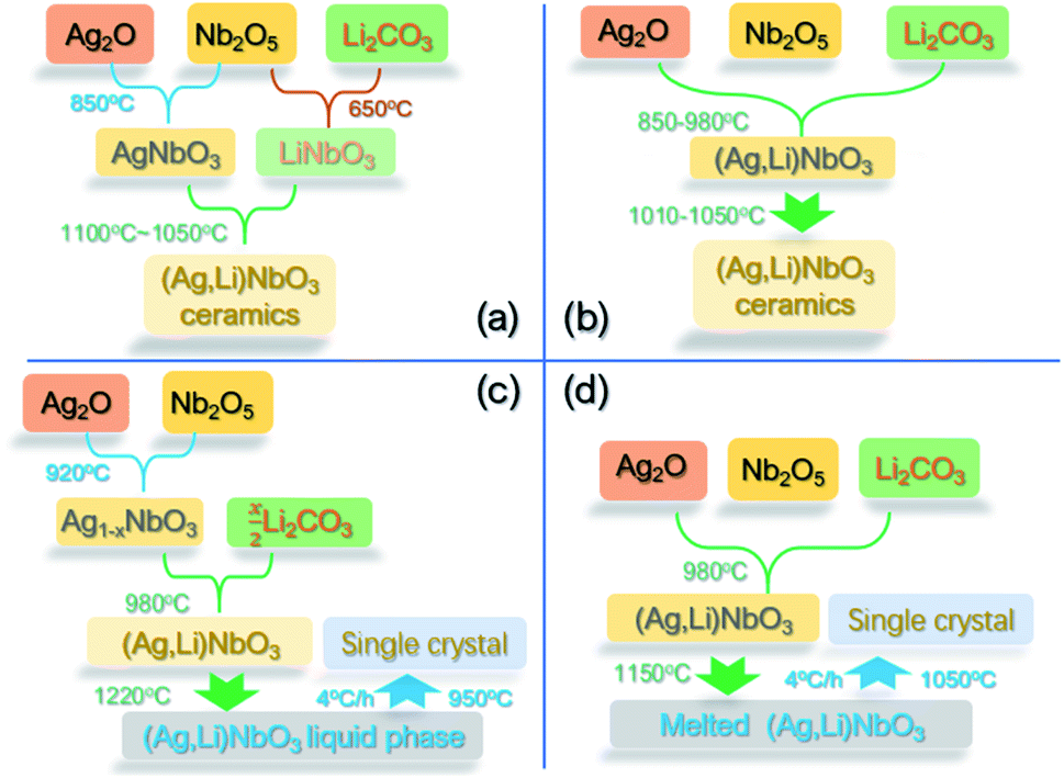 | ||
| Fig. 25 Schematic synthesis procedures for (Ag,Li)NbO3 ceramics reported by (a) Niewiadomski et al.,97 and A. Kania et al.,101 and (b) Fu et al. and Khan et al.;102,103 schematic synthesis procedures for (Ag,Li)NbO3 single crystals reported by (c) Wada et al.99 and (d) Fu et al.69 | ||
The synthesis of ALN single crystals using the procedures shown in Fig. 25c and d also results in different structure and properties. It was reported that ALN thin films can be fabricated on (001), (110) and (111) SrTiO3 (STO) substrates by pulsed laser deposition (PLD),104 while the ALN ceramic targets for fabricating thin films were prepared by a solid-state reaction method, being similar to the processing reported by Fu et al.102
3.2.1.2 Composition–structure–property relationships. The composition–structure–property relationships in ALN solid-solutions reported in previous publications50,67,90,91,99–101 differ with respect to the different processing conditions used. As demonstrated above, using the synthesis approach described in Fig. 24a, bi-phasic ceramics (i.e., ALN solid-solution and LiNbO3) are obtained when x > 0.03 mol. Diffraction analysis of samples prepared using the synthesis method reported by Fu et al.102 (see Fig. 26b), shows that the solubility limit of Li is near x = 0.1 and a composition-driven transition from orthorhombic to rhombohedral (O–R) phases was found in the range x = 0.05 to 0.06, above which, the ALN solid-solution exhibits a single rhombohedral ferroelectric phase, as shown in Fig. 26a. Significant property variation was also revealed in ALN ceramics, giving additional evidence to support a composition-driven phase transition. With increasing x-value, a significant change in the dielectric behavior is observed (Fig. 26b), with a sharp maximum peak found at x ≥ 0.06.102 This peak shifts to higher temperature with further increase of the x-value. The temperature corresponding to the dielectric peak is believed to be the Curie point (TC) of the FE R phase. Fu et al.102 proposed that as the x-value increases, the FE R phase develops from the FE structure originally found in the M1 region. However, further examination of the dielectric pattern reveals that the dielectric anomaly TI (assigned to the M1 ↔ M2 transition) gradually shifts to lower temperature and disappears for x > 0.06. Thus, the M1 ↔ M2 transition could correspond to a local structural evolution rather than to a symmetry change, as proposed in our previous study on AgNbO3.16 The double P–E hysteresis loops evolve into a ferroelectric-type loop when the composition approaches the AFEO/FER phase boundary, consistent with the structure characterization. The ALN single crystals prepared using the procedure described in Fig. 25d reported by Fu et al.69 also show similar results to the ceramic samples. Interestingly, the investigation on ALN single crystals, prepared using the procedure shown in Fig. 25c reported by Wada et al.,96 highlights a structural change from the AFE orthorhombic (Pbcm) phase to an FE orthorhombic (Pc21b) phase at x = 0.07. On further increasing the x-value, an extra composition-driven FE orthorhombic (Pc21b) to FE rhombohedral (R3c) phase transition occurred at x = 0.1 (see Fig. 26d). For x > 0.1, this phase transition shifts to higher temperature, indicating the possible presence of an intermediate structure connecting the AFEO and FER phases. It is possible that the range of this intermediate structure is dependent on the quality of samples.
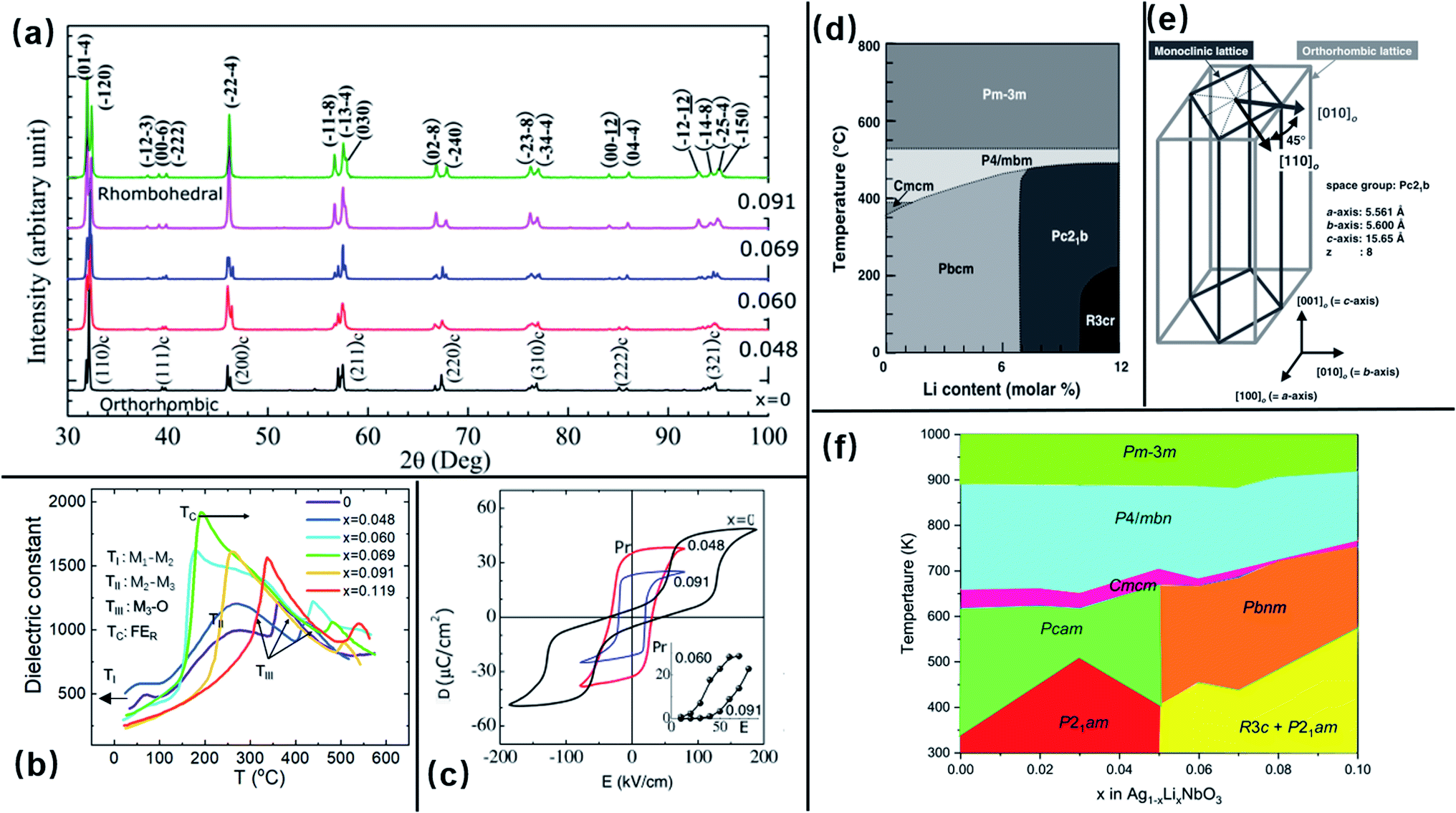 | ||
| Fig. 26 (a) XRD patterns of synthesized powder, (b) temperature-dependent dielectric permittivity and (c) P–E loops of Ag1−xLixNbO3 ceramic solid-solutions reported by Fu et al. in 2011.102 [Reproduced from ref. 102https://doi.org/10.1088/0953-8984/23/7/075901 with permission from copyright IOP Publishing]. (d) Schematic phase diagram of ALN system (using the preparation procedure shown in Fig. 25c) and (e) schematic configuration of [010]o and [110]o directions for Pc21b orthorhombic symmetry reported by Wada et al. in 2006;96 [reproduced from ref. 96https://doi.org/10.1143/JJAP.45.7389 with permission from copyright IOP Publishing]. (f) Schematic phase diagram of ALN system reported by Farid et al. in 2020 (using the preparation procedure shown in Fig. 25b).52 [Reproduced with permission from ref. 52 copyright 2020 American Chemical Society]. | ||
It should be noted that the FEOPc21b structure exhibits the same unit-cell dimensions  as the AFEOPbcm structure (see Fig. 26d). After the FIE structure of AgNbO3 was identified in 2011,49 Farid et al.52 re-investigated the structural evolution of ALN powders synthesized by the method described in Fig. 25b, using high-resolution ND and synchrotron XRD. They suggested a new phase diagram for the ALN system, where the coexistence of FIE P21am (axial transformation of Pmc21) and FE R3c phases was found for x > 0.05. In addition, for x > 0.05, a distinct polymorphic phase behavior compared to that of pure AgNbO3 on heating was proposed: both P21am and R3c polar structures evolved into a non-polar Pbnm phase and caused the maximum dielectric peak (TC) shown in Fig. 26b. By means of electron diffraction (ED), additional structural details for the x > 0.05 compositions were revealed. The ED study by Khan et al.103 reported a new complex modulated oxygen octahedral tilt system with a
  unit-cell, which could be considered as an intermediate structure bridging the AFEO phase and the FER phase. Such intermediate modulated structures are not unusual in anti-/ferroelectric perovskites and have been found near the MPB in many solid solutions, such as BNT-based and BFO-based perovskites, due to the complex interaction between off-centering cation displacements and oxygen octahedral tilting.105–109 Thus, it is hard to describe the exact structural nature of the so-called MPB region based on the coexistence of two or more well-defined crystallographic phases. Therefore, more structural investigations are needed to deepen the understanding of the MPB region in ALN solid solutions.
 | ||
| Fig. 27 (a) A schematic drawing reflecting the structure–property relationships present in the ANLT100x system in the form of symmetry modes, phases and electrical properties; (b) composition-driven variation of lattice parameters of orthorhombic Pmc21 and rhombohedral R3c phases, as well as the phase fraction of the R3c phase; (c) temperature-dependent dielectric spectrum of ANLT100x reported by Lu et al.53 Evolution of Pr (d) and P–E hysteresis loops during bipolar cycling measured on ANLT4.5 (50 kV cm−1 and 10 Hz) and ANLT6 (30 kV cm−1 and 10 Hz). (f) Temperature-dependent dielectric permittivity and loss tangent (at 10 kHz) of pristine, intermediate (IM), and “woken-up” (three conditions) ANLT4.5 ceramics; (g) neutron diffraction pattern of selected peaks collected under the three conditions. (h) R3c phase fraction, with cation displacements along the c-axis for the pristine, IM, and “woken-up” conditions of ANLT4.5 and ANLT6 ceramic reported by Lu et al.110 [(d–h) are reproduced with permission from ref. 110 copyright 2020 American Chemical Society]. | ||
 | ||
| Fig. 28 (a) Schematic diagram of the measurement circuit for BNBT6–ANLT6 dual capacitors and (b) evolution of normalized Pr during bipolar cycling measured on a BNBT6 capacitor and a BNBT6–ANLT6 dual capacitor reported by Lu et al.110 [Reproduced with permission from ref. 110 copyright 2020 American Chemical Society]. (c) Temperature-dependent pyroelectric coefficient (p) for poled ANLT100x ceramics; (d) Olsen cycle diagram of pyroelectric energy harvesting for the ANLT5 ceramic reported by Li et al.111 | ||
Li et al.111 recently reported that the ANLT solid-solution also exhibits excellent pyroelectric properties during the depolarization process of the electric field-induced FE state (see Fig. 28c). ANLT compositions with x ≥ 0.04 exhibit a high pyroelectric coefficient p ≈ 3–3.7 × 10⁻⁸ C cm−2 K−1 at room temperature and an ultrahigh peak value (p = 120–160 × 10−8 C cm−2 K−1) at the depolarization temperature (Td). If Td could be adjusted to room temperature, these materials could have important applications as pyroelectric detectors. It is well-known that field-induced transitions can cause an enhancement of dielectric response via the creation of an MPB, providing an extra contribution to the total pyroelectric coefficient. Li et al.111 also studied the pyroelectric energy harvesting performance of ANLT5 ceramics. The energy harvesting process can be achieved using an Olsen cycle,112 as schematically shown in Fig. 28d, while the harvested pyroelectric energy density (W) can be estimated from the area of the blue region shown in the figure. The harvested energy between 30 °C and 190 °C was estimated to be about 1.4 J cm−3, which holds promise for energy harvesting.
 | ||
| Fig. 29 (a) Composition-driven variation of pseudo-cubic parameters and (b) temperature-dependent dielectric pattern of (Ag1−xKx)NbO3 solid-solution reported by Fu et al.114 [Reproduced from ref. 114https://doi.org/10.1063/1.3259410 with the permission of AIP Publishing]. The temperature TFEC was assigned by Fu et al.13 to the Curie point, due to the discovered weak-FE/FIE Pmc21 structure reported by Yashima et al. in 2011.49 The temperature TAFEC indicates the Curie temperature of the AFE phase; the other dielectric anomalies were assigned to the M1 ↔ M2 transition, Tf and the M2 ↔ M3 transition by Kania et al. in 1983.14 | ||
The dielectric behavior of the AKN system also exhibits significant changes upon composition modification, as shown in Fig. 29b. Observing the variation of the temperature-dependent dielectric behavior with composition, it can be noticed that the dielectric anomalies assigned to the M1 ↔ M2 and M2 ↔ M3 phase transitions are gradually suppressed, and a sharp peak denoted as Tc1 can be found at x = 0.07. Furthermore, another anomaly denoted as Tc2 can be noticed near 150 °C, the origin of which is still unclear. Below Tc2, the structure could be FE Pmc21 as reported in a recent paper.117 Therefore, the dielectric anomaly denoted as Tc2 could correspond to the Tf transition or to the TC of the FIE phase, as reported for the case of AgNbO3.16,74 This would indicate that the FIE phase was gradually replaced by an FE phase. There are no studies clarifying the structural nature in the range between Tc2 and Tc1; hence, the question whether this phase is AFE is still unsettled. Most recently, Liu et al.117 investigated the pressure-induced variations of structure and properties in the AKN system. A composition–pressure phase diagram is outlined in Fig. 30a. The FE–AFE (note: the authors refined the structure using the AFE Pbcm model and not the FIE Pmc21 model) transition can occur when the loading pressure reaches 350 MPa for x = 0.065 (Fig. 30a and b). Meanwhile, this material shows a very high charge release density (∼37 μC cm−2) under a shock pressure of 6.9 GPa (Fig. 30c). The simulated energy density of this material is about 5.401 J g−1, which is significantly higher than in other FE ceramics (Fig. 30d). The high discharge energy density after shock pressure gives a potential application for explosive energy conversion. It is noticed that after shock-pressure loading, a “double” hysteresis with non-zero remnant polarization can be observed in Fig. 30b. This feature may indicate that the pressure-induced structure is not AFE, but FIE.
 | ||
| Fig. 30 (a) Pressure–composition phase diagram of the (Ag0.935K0.065)NbO3 (AKN065) system; (b) pressure-dependent polarization–electric field (P–E) loops of AKN065 ceramics measured at room temperature; (c) dynamic discharging response of assembled AKN065 ceramic devices collected under a shock pressure of 6.9 GPa; and (d) comparison of the energy storage densities per unit weight of the AKN065 ceramics and other FE materials, reported by Liu et al.117 | ||
3.3 AgNbO3-based antiferroelectric solid-solutions
In the early studies of AgNbO3, various solid-solutions, such as AgNb1−xTaxO3, were intensively studied due to their excellent dielectric properties.19 Measurements performed in the 1 GHz region showed εr ≈ 400, Q × f ≥ 700 GHz, and Δf/f = 0–0.22 in the temperature range −40 to 60 °C for a composition close to AgNb0.5Ta0.5O3,19 which represents an attractive material for high-frequency applications. In recent years, due to the development of new types of energy storage technologies, various research teams have started devoting their attention to AgNbO3-based antiferroelectric materials, due to their double P–E loops. The field-induced phase transition can be significantly influenced by the concentration of doping elements, giving rise to enhanced energy storage performance compared to non-doped AgNbO3. In this section, a detailed survey of the previous fundamental studies on AgNbO3-based antiferroelectric materials is provided with the aim of identifying a general principle to optimize the related performance, as well as providing guidelines for future studies. | ||
| Fig. 31 (a) Temperature-dependence of dielectric permittivity and loss tangent for NaNbO3 as reported by Kania et al.;54 [reproduced from ref. 54https://doi.org/10.1088/0953-8984/11/45/316 with permission from copyright IOP Publishing]. (b) The reported phase transitions of NaNbO3 studied using X-ray diffraction. Note: the structural nature of the P phase, as well as its temperature stability range are still controversial (see ref. 119, Fig. 1). | ||
The high temperature phases (cubic, tetragonal and orthorhombic) have been carefully studied and have been found to be isostructural with the three paraelectric phases of AgNbO3.47,120 At room temperature, the structure of ceramic samples prepared by conventional solid-state reaction is orthorhombic AFE, which is isostructural with AgNbO3, although some publications have also reported the existence of a metastable FEO phase in local regions.121,122 At low temperature, the structure of ceramic samples displays a FE R3c phase, which is isostructural with the FE phase reported in ALN or ANLT systems, as discussed in Section 3.2.1.2. Previous studies on the Ag1−xNaxNbO3 (ANN) solid-solution are rare. It has been reported that ANN compositions can be obtained via conventional solid-state reaction and sintering in O2 atmosphere.54 AgNbO3 and NaNbO3 should form a continuous solid-solution due to their similar crystalline structures.46 However, the temperature–composition diagram proposed by Fu et al.123 indicates that a phase boundary exists when the concentration of Na+ ions exceeds 0.8, as shown in Fig. 32a. It is not clear whether in the composition range 0.8 < x < 0.9, a solid-solution can be formed; therefore, further studies on these compositions are needed. Kania et al.54 investigated the dielectric spectroscopy of the ANN system (see Fig. 32b and c) to understand the microscopic mechanisms that contribute to the appearance of a diffuse dielectric peak at around 270 °C (denoted as the M2 ↔ M3 transition in AgNbO3).
 | ||
| Fig. 32 (a) Variation of transition temperatures in the Ag1−xNaxNbO3 system derived from the dielectric measurements reported by Fu et al.123 [Reproduced from ref. 123https://doi.org/10.1063/1.3609234 with the permission of AIP Publishing]. Temperature-dependence of dielectric permittivity in Ag1−xNaxNbO3 (b) on heating and (c) on cooling, reported by Kania et al.54 [Reproduced from ref. 54https://doi.org/10.1088/0953-8984/11/45/316 with permission from copyright IOP Publishing]. | ||
The diffuse dielectric response in the Ag1−xNaxNbO3 system has attracted great research interest for high-frequency applications. The temperature dependence of the dielectric permittivity (see Fig. 32b) shows that the high-temperature anomaly gradually shifts to higher temperature with increasing Na concentration, up to x = 0.6, and starts shifting to lower temperature at higher Na content, with an increase in the value of the dielectric permittivity near the transition point. The low temperature anomaly monotonously shifts to higher temperature with increasing Na concentration, while the dielectric permittivity decreases near the transition point. The gradual suppression of the diffuse dielectric anomaly with increasing Na+ ion concentration can be more clearly observed in the dielectric pattern obtained during cooling (see Fig. 32c). In particular, upon cooling, the dielectric peak corresponding to the AFE–PE transition presents a negligible shift with composition. Kania et al.54 proposed that Na substitution causes a decrease of the oxygen octahedron size, diminishing the freedom of Nb5+ ions, resulting in a gradual decrease of the diffuse dielectric anomaly. This viewpoint is consistent with the gradual decrease of the t-factor due to the occupation of the A-site by Na+, which makes it harder for the Nb5+ ions to move off-center in their oxygen octahedra. Furthermore, it was reported that this solid-solution exhibits a large electric field-induced strain response of about 0.2% over the wide compositional range 0.4 < x < 0.8 (see Fig. 33), which might be interesting for the development of lead-free actuators.
 | ||
| Fig. 33 P–E and S–E hysteresis loops of ANN solid-solution reported by Fu et al.123 [Reproduced from ref. 123https://doi.org/10.1063/1.3609234 with the permission of AIP Publishing]. | ||
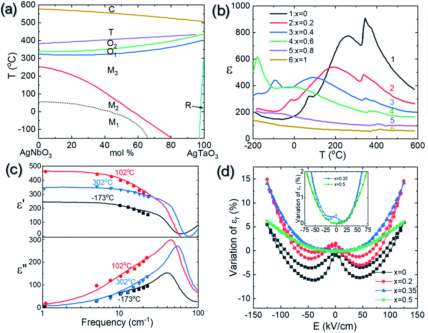 | ||
| Fig. 34 (a) Temperature–composition phase diagram of the AgNb1−xTaxO3 reported by Pawełczyk et al.55; [reproduced from ref. 55https://doi.org/10.1080/01411598708220073 with permission from Taylor & Francis Informa Ltd]. (b) Temperature-dependent dielectric pattern of the AgNb1−xTaxO3 system original reported by Kania et al.;129 [reproduced with permission from ref. 129https://doi.org/10.1080/01411598308244116 with permission from Taylor & Francis Informa Ltd]. (c) The dielectric dispersion in the millimeter and submillimeter wave region of AgNb0.6Ta0.4O3 as calculated from the oscillator and relaxor additive model (solid lines) at different temperatures; points are experimental values reported by Volkov et al.;58 [reproduced from ref. 58https://doi.org/10.1088/0953-8984/7/4/009 with permission from copyright IOP Publishing]. (d) Variation of dielectric permittivity of AgNb1−xTaxO3 ceramics at 100 kHz with a maximum electric field bias of 125 kV cm−1 as reported by Li et al.131 [Reproduced from Ref. 131https://doi.org/10.1063/1.4875581 with the permission of AIP Publishing]. | ||
| Samples | P max [μC cm−2] | P r [μC cm−2] | E F [kV cm−1] | E B [kV cm−1] | ΔE [kV cm−1] |
|---|---|---|---|---|---|
| AN | 35.9 | 3.6 | 110 | 52 | 58 |
| ANT5 | 37.2 | 2.0 | 153 | 95 | 58 |
| ANT10 | 35.5 | 1.9 | 166 | 110 | 56 |
| ANT15 | 36.8 | 1.7 | 189 | 130 | 59 |
| ANT20 | 31.5 | 1.2 | 222 | 163 | 59 |
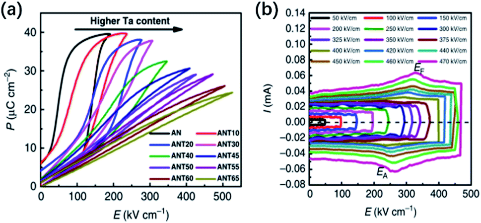 | ||
| Fig. 35 (a) P–E loops of ANT100x ceramics and (b) I–E loops of ANT55 ceramics reported by Luo et al.17 | ||
| Chemical formula | Mineral | Crystal system | Space group |
|---|---|---|---|
| Bi1/3NbO3 (Bi3NbO9) | Perovskite | Tetragonal | P4/mmm |
| La1/3NbO3 | Perovskite | Orthorhombic | Pmmm or Cmmm |
| Ce1/3NbO3 | Perovskite | Monoclinic | P2/m |
| Pr1/3NbO3 | Perovskite | Orthorhombic | Cmmm |
| Nd1/3NbO3 | Perovskite | Orthorhombic | Cmmm |
In 2006, Hu et al. successfully prepared a bismuth-modified AgNbO3 solid-solution (Ag1−xBix/3NbO3).136 The structure analysis suggested that about 20 mol% of Bi3+ ions can be incorporated into the lattice of AgNbO3 to form a perovskite structured solid-solution without impurity phases, implying that 40% of the A-sites are vacant. A dielectric study on this solid-solution indicated that all dielectric anomalies shift to lower temperature and the diffuse dielectric peak corresponding to the M2 ↔ M3 transition becomes broader with increasing Bi concentration (see Fig. 36). In particular, the dielectric permittivity is almost independent on temperature in the range from −50 °C to 50 °C for some compositions, making them of interest for capacitor applications. When x ≥ 0.4, the sharp maximum corresponding to the AFE–PE phase transition disappeared and the response of a typical relaxor was observed. Our research team has also successfully prepared Ag1−3xBixNbO3 solid-solutions with high-quality.137 The dielectric response under DC field reveals that the ferrielectric/weak-ferroelectric behavior progressively disappears when x reaches 0.04 (corresponding to x = 0.12 according to the chemical formula reported by Hu et al.136), as shown in Fig. 37a. Above x = 0.04, the ceramic samples exhibit a single AFE phase. The enhanced antiferroelectric stability is evidenced by the D–E loops under strong-field cycling as shown in Fig. 37b. By increasing the Bi3+ ion concentration, the characteristic fields of the AFE–FE field-induced transition increase, indicating a higher energy barrier between AFE and FE phases.
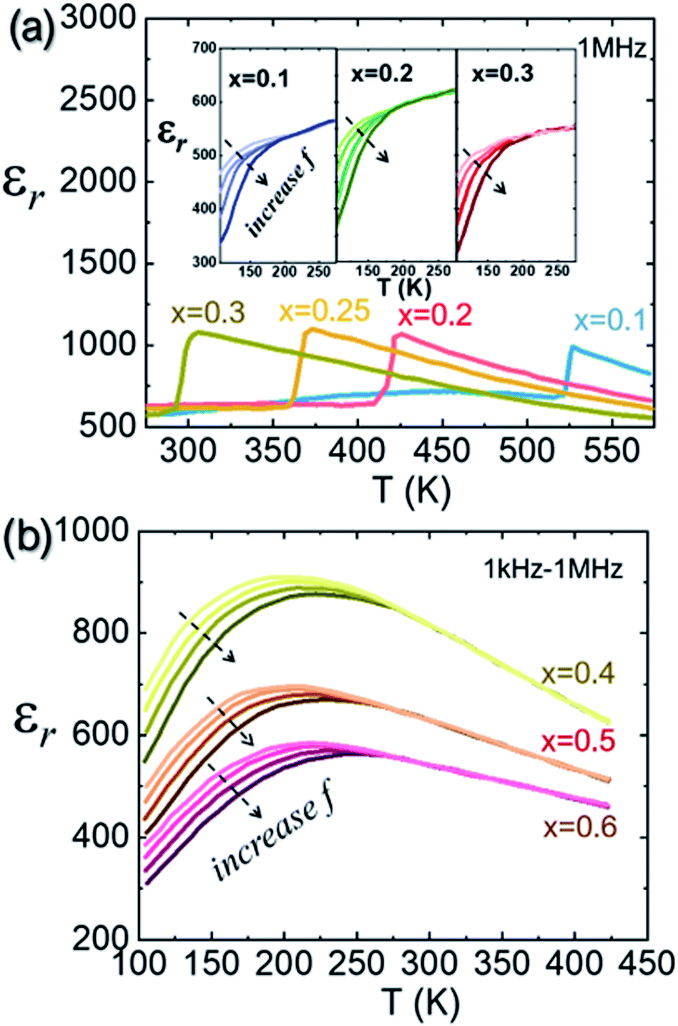 | ||
| Fig. 36 Temperature-dependent dielectric spectra of Ag1−xBix/3NbO3 ceramics reported by Hu et al.136 [Reproduced from ref. 136https://doi.org/10.1063/1.2209552 with the permission of AIP Publishing]. | ||
 | ||
| Fig. 37 (a) Percentage variation in relative permittivity (εr) at low DC field in (Ag1−3xBix)NbO3 (ABNx) ceramics, and (b) high-field ferroelectric D–E loops of ABNx ceramics reported by Tian et al.137 | ||
Based on the design and the successful preparation of the A-site deficient Ag1−3xBixNbO3 solid-solution, a series of other A-site deficient Ag1−3xLnxNbO3 (Ln: rare-earth elements, x < 0.05) ceramics have been subsequently reported,138–141 in the search for new materials with improved energy storage performance.
The temperature dependence of the dielectric permittivity of various A-site deficient compounds is reported in Fig. 38. It can be noticed that La3+ doping induces similar trends to those produced by Bi3+ doping, while Sm3+ and Gd3+ doping shifts the maximum dielectric peak related to the AFE–PE transition with a decrease of the dielectric permittivity. The transition almost disappears for 4 mol% Sm3+ and Gd3+ doping. This might suggest that the dopant elements are also present on the B-site of the AgNbO3 lattice, resulting in composition fluctuation and breaking of the AFE distortion. These features also suggest that the solubility limit of Sm3+/Gd3+ in AgNbO3 is around 4 mol%. As with Bi-doped AgNbO3, the characteristic field EF increases with increasing Ln3+ concentration, while the field-induced polarization visibly reduces as shown in Fig. 39a–c. The composition-driven property variation is very similar to the changes observed in the ferroelectric loops of AKN6 ceramics with increasing pressure shown in Fig. 39d.117 Similar phenomena have also been observed in rare-earth substituted BiFeO3, in which the field-induced FE polarization is significantly suppressed at high concentrations of rare-earth dopants.108,109 It can be inferred that the reduced t-factor weakens the AFE distortion and reduces the freedom of cation displacement. In addition to Ln3+-doped AgNbO3, alkaline earth elements such as Ca2+ have been also used as dopants for AgNbO3 and showed similar effects to La3+ doping.143
 | ||
| Fig. 38 Temperature-dependent dielectric spectra of (a) Ag1−3xBixNbO3 (reported by Tian et al.137); (b) Ag1−3xLaxNbO3 (reported by Gao et al.142); (c) Ag1−3xSmxNbO3 (reported by Gao et al.138) [reproduced with permission from ref. 138 copyright 2020 American Chemical Society] and (d) Ag1−3xGdxNbO3 (reported by Li et al.140). | ||

 | ||
| Fig. 40 P–E loops of (a) (1 − x)AgNbO3–xCaTiO3 (ref. 144) [reproduced with permission from ref. 144 copyright 2020 by Elsevier]; (b) (1 − x)AgNbO3–x(Bi0.5Na0.5)TiO3,145 [reproduced with permission from ref. 145 copyright 2020 by Elsevier] and (c) Bi(Zn2/3Nb1/3)O3 (BZN) concentration dependence of relative permittivity of (1 − x)AN–xBZN ceramics before and after poling.147 | ||
4. AgNbO3-based materials for high-power energy storage
The direct way to calculate the total stored energy density (W) of a dielectric material is through integration of the D–E curve: | (3) |
 | (4) |
 | (5) |
 | ||
| Fig. 41 Schematic energy storage density (colored area) of (a) linear dielectrics, (b) ferroelectrics, and (c) antiferroelectrics under the same applied electric field. | ||
From Fig. 41, it is clear that under the same applied field, antiferroelectrics should display higher energy density compared to the other types of dielectrics. A summary of the energy storage performances of AgNbO3-based antiferroelectric materials is reported in Table 5. It can be noticed that the value of Wrec in chemically-modified AgNbO3 ceramics can reach 6 J cm−3, which is three times that of unmodified AgNbO3 ceramics. Besides the composition modification, the Wrec of AgNbO3-based ceramic capacitors can be greatly improved through multilayer chip ceramic technology, as reported by Zhu et al. in a recent study.148 In particular, an AgNbO3 epitaxial film grown on a (001) STO substrate reported by Zhang et al. showed an ultrahigh characteristic field EF (∼250 kV cm−1) while the EB remained unchanged compared to an AgNbO3 ceramic sample. Nevertheless, the film showed a higher Wrec than the ceramic sample of AgNbO3.44
| Materials compositions | D max (μC cm−2) | E F (kV cm−1) | ΔE (kV cm−1) | E b (kV cm−1) | W rec (J cm−3) | η (%) | Ref. |
|---|---|---|---|---|---|---|---|
| a BZN: Bi(Zn1/3Nb2/3)O3; BNT: Bi0.5Na0.5TiO3; CT: CaTiO3; CTH: Ca(Ti,Hf)O3; ANT15: Ag(Nb0.85Ta0.15)O3. | |||||||
| AgNbO3 (AN) | 41 | 125 | 75 | 175 | 2.1 | 39 | 15 |
| AN epitaxial film | ∼40 | ∼250 | ∼200 | 624 | 5.8 | 55.8 | 44 |
| AN–0.1 wt% WO3 | ∼42 | ∼165 | 75 | 200 | 3.3 | 50 | 149 |
| AN–0.1 wt% MnO2 | 37 | 117 | 54 | 150 | 2.5 | 57 | 150 |
| Ag0.97Bi0.03NbO3 | 26 | — | — | 205 | 2.6 | 86 | 137 |
| Ag0.94La0.02NbO3 | ∼28 | ∼250 | ∼75 | 273 | 4.4 | 73 | 139 |
| Ag0.94La0.02NbO3 | ∼30 | ∼175 | ∼75 | 230 | 3.12 | 63 | 151 |
| Ag0.94Sm0.02NbO3 | ∼30 | ∼270 | ∼80 | ∼300 | 4.5 | 63 | 138 |
| Ag0.91Sm0.03NbO3 | ∼38 | ∼225 | ∼75 | ∼290 | 5.2 | 68 | 141 |
| Ag0.97Sm0.01NbO3 | ∼40 | ∼125 | ∼40 | ∼175 | 3.8 | 73 | 152 |
| Ag0.88Gd0.04NbO3 | ∼34 | ∼250 | 80 | 290 | 4.5 | 63 | 140 |
| Ag0.97Nd0.01NbO3 | ∼40 | ∼150 | ∼70 | 210 | 3.2 | 52 | 153 |
| Ag0.92Ca0.04NbO3 | 39 | 179 | 80 | 220 | 3.5 | 56 | 143 |
| Ag(Nb0.85Ta0.15)O3 | ∼37 | 189 | 59 | 240 | 4.2 | 69 | 132 |
| Ag(Nb0.8Ta0.2)O3 | 37 | 175 | 55 | 270 | 3.7 | 58 | 78 |
| Ag(Nb0.45Ta0.55)O3 | ∼28 | ∼300 | ∼60 | 470 | 6.3 | 90 | 17 |
| ANT15 multilayer ceramic | ∼44 | ∼190 | ∼90 | 1020 | 7.9 | 71 | 148 |
| Sm0.02Ag0.94Nb0.9Ta0.1O3 | 38.5 | ∼220 | ∼80 | 280 | 4.87 | 63.5 | 154 |
| Nd0.01Ag0.97Ta0.2Nb0.8O3 | ∼40 | ∼275 | ∼75 | 370 | 6.5 | 71 | 155 |
| Ag0.94La0.02Nb0.8Ta0.2O3 | ∼50 | ∼300 | ∼100 | ∼400 | 6.9 | 71 | 156 |
| Ag0.9Ca0.05Nb0.95Ta0.05O3 | ∼30 | ∼190 | ∼120 | 210 | 3.36 | 58.3 | 157 |
| 0.99AN–0.01BZN | 54 | 198 | 80 | 220 | 4.6 | 57 | 147 |
| 0.97AN–0.03BNT | 35 | 180 | 80 | 220 | 3.4 | 62 | 145 |
| 0.98AN–0.02CT | 40 | 190 | 90 | 220 | 3.7 | 52 | 144 |
| 0.94AN–0.06CTH | 40 | 266 | 98 | 300 | 5.4 | 66 | 158 |
The energy storage efficiency in these materials is usually less than 70%. The main advantage of antiferroelectric capacitors compared to linear dielectrics is the possibility of a large field-induced polarization under certain applied electric fields. An increase of the characteristic field EF can give rise to an enhancement of Wrec for an antiferroelectric material. Another key parameter to impact the energy storage performance is the degree of hysteresis. Nano-structured domains or polar nanoregions (PNRs) generally found in relaxor-ferroelectrics lead to slim D–E loops accompanied by a large FE polarization, as observed in PbMg1/3Nb2/3O3 and BaTiO3-based compounds. Therefore, further efforts should be directed to develop AgNbO3-based relaxors/anti-/ferroelectrics as proposed in Fig. 42 to improve the energy efficiency η.
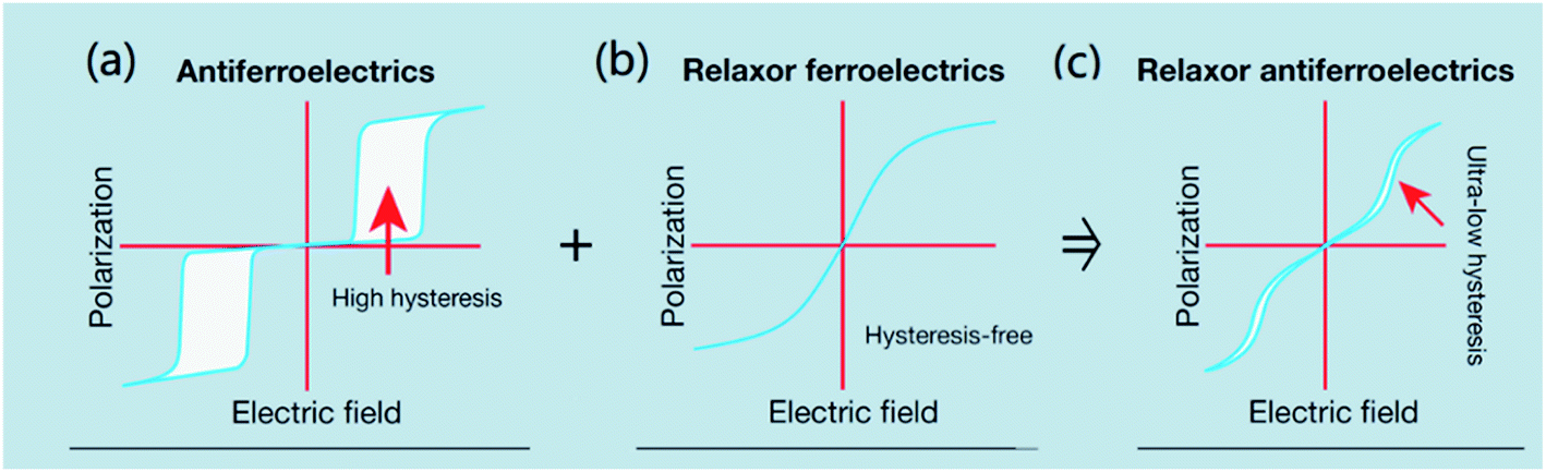 | ||
| Fig. 42 Schematic strategy to develop AgNbO3-based antiferroelectrics for practical applications159 [reproduced with permission from ref. 159 copyright 2019 by Elsevier]. | ||
Considering practical applications of dielectric capacitors, the energy storage capability per unit volume of a linear dielectric material can generally be estimated using the following expression:160
 | (6) |
 | ||
| Fig. 43 Electrical breakdown strength (Eb, BDS) of AgNbO3-based ceramics as a function of grain size: (a) small grain sizes and (b) large grain sizes. | ||
Additionally, it is generally believed that the sample thickness has a significant effect on the Eb, because fewer defects exist in thinner layers.170–172 More interestingly, Eb can be significantly improved through microstructural design, such as introducing core–shell features, with a ferroelectric core and a non-ferroelectric (e.g. paraelectric) shell.173,174
5. AgNbO3-based materials for photocatalysis
Semiconductor-based photocatalytic technologies have been extensively investigated since 1972,20 for the production of renewable hydrogen from water and for the degradation of organic pollutants by photo-generation of electricity and photoelectrochemical reactions.175–177 AgNbO3-based perovskites were reported to exhibit visible-light-driven photocatalysis activity due to their narrow band gap (2.08–2.93 eV),81 which has attracted increased research interest over the past decade. The following sections will give a detailed review of photocatalysis associated with AgNbO3-based materials.5.1 Fundamental principles of semiconductor photocatalysis
The underlying mechanisms of the photocatalysis process have been extensively discussed in textbooks and in primary literature.178–180 Here, a brief introduction to the fundamental principles of semiconductor photocatalysis is provided. The principle of photocatalytic degradation of water pollutants is schematically shown in Fig. 44a. Upon light-illumination, with photons of larger energy (E = hν) than the band gap (Eg) of the semiconductor, electrons will be excited from the valence band to the conduction band, generating an equal number of free electrons and holes. The excited electrons and holes will be separated and will migrate to the surface of the semiconductor. The photo-generated electrons could reduce a dye or react with electron acceptors, such as the O2 molecules adsorbed on the surfaces of the semiconductor, generating superoxide radical anions (˙O2−). The photo-generated holes can oxidize organic substances or react with electron donors, such as OH−, resulting in hydroxyl radicals (˙OH). The hydroxyl radicals can oxidize most dyes into mineral end-products due to their strong tendency to oxidation (standard redox potential +2.8 V). | ||
| Fig. 44 (a) A schematic of the photocatalytic mechanism in semiconductors for degrading an organic pollutant; (b) a schematic illustration of the fundamental principles of a semiconducting photocatalytic water-splitting process; (c) energy diagrams for photocatalytic water-splitting, and (d) a schematic illustration of the fundamental principles for a semiconducting photoelectrochemical water-splitting process.184 [Reproduced with permission from ref. 184 copyright 2018 by John Wiley and Sons]. | ||
The processes of generating hydrogen from water under light irradiation can be mainly classified into two reaction categories: (1) photocatalytic; and (2) photoelectrochemical.180 The photocatalytic reaction process for hydrogen production is very similar to the process of water pollutant degradation, but usually involves a heterogeneous co-catalyst (such as TiO2–Pt powder).181 The photocatalytic reaction of water splitting is schematically shown in Fig. 44b. During light-illumination, the semiconductor photocatalyst is first excited by absorbing photons, generating an equal number of electrons and holes; then, water molecules are reduced by the photo-generated electrons to form H2 and are oxidized by the photo-generated holes to form O2. To ensure the occurrence of these photocatalytic reactions and achieve water-splitting, the energy band of a semiconductor-based photocatalyst should straddle the redox potentials of water. In particular, the bottom of the conduction band has to be more negative than the redox potential of H+/H2 (0 V versus standard hydrogen electrode (SHE)), while the top of the valence band has to be more positive than the redox potential of O2/H2O (1.23 V), as shown in Fig. 44c.
The generation of hydrogen by photoelectrochemical reaction is usually achieved in a photoelectrochemical cell (PEC), which consists of a photoelectrode (i.e., a semiconductor-based photocatalyst such as TiO2), a counter electrode (typically Pt or graphite) and an electrolyte solution.182,183 The fundamental photoelectrochemical reaction is schematically shown in Fig. 44d for a TiO2–Pt PEC as an example. TiO2 is a well-known n-type semiconductor, and can work as a photoanode in the PEC, while Pt serves as a counter electrode. Upon light-illumination, photo-excited electrons and holes are generated in the conduction band and valence band of TiO2, respectively, and then, the photo-generated electrons are transferred and transported onto the surface of the counter electrode, Pt, through an external circuit with ohmic contacts, where H+ is reduced to H2. Concurrently, the photo-generated holes can favor the oxygen evolution reaction at the surface of the TiO2 photoanode, generating O2. It is noted that if a p-type semiconductor is used as the photocatalyst, it would usually act as a photocathode for hydrogen evolution. When comparing the PEC to powdered photocatalytic processes using a co-catalyst, the powdered co-catalyst system can be considered as a short-circuit version of a PEC since the photocatalytic reactions are spatially separated on the powdered catalyst and occur on a much shorter length scale than that for the PEC. The advantage of the PEC is that it can be more effective in separating photo-generated electrons and holes on the macroscale using different electrodes and in decreasing recombination, but the cost for industrial production of long-life and efficient PECs is high. The powdered catalyst, instead, shows an easier process and holds great potential due to its much lower costs, although its catalytic efficiency is lower than that of a PEC.
5.2 Fundamentals of ferroelectric photocatalysis
Currently, great efforts have been devoted to improve the photocatalytic activity of powdered catalysts, mainly including: (1) the search for semiconductors with a narrow band gap (for providing a maximum utilization of solar energy especially in the visible light range);185–187 (2) microstructure optimization by controlling the particle size, and by establishing a balance between large specific surface areas (providing a high density of available reaction sites) and transport pathways for photo-generated charge carriers (affecting recombination rates and back reaction);176,188 (3) decoration of the surface with a metallic co-catalyst; (4) introduction of heterogeneous interfaces such as hetero-junctions, to create an internal electric field for enhancing the separation rate of photo-generated charge carriers.180,189–191Additionally, the internal electric field induced by the spontaneous polarization (Ps) of a ferroelectric has been considered an important factor in photocatalytic performance.192,193 AgNbO3 is a weak-ferroelectric/ferrielectric compound possessing a narrow band gap ((2.08–2.93 eV)).21,81 Ambient ferroelectricity with large Ps can be obtained in doped compounds, such as ALN and AKN solid-solutions,69,117 which could represent potential candidates for ferroelectric photocatalysts.
In ferroelectrics, the intrinsic Ps can generate bound charges on the ferroelectric surfaces/interfaces. These bound charges are not energetically stable and can be compensated in two ways: internal screening and/or external screening,194 as schematically shown in Fig. 45a. The internal screening can be realized by the flow of free charge carriers within the ferroelectric crystal, whereas external screening is achieved by the adsorption of charged ions and molecules on the surface of the crystal from the surrounding media. Internal screening by the flow of free charge carriers redistributes the charge carriers near the surface, leading to band bending and a space charge region (SCR),195 as schematically shown in Fig. 45b. If the ferroelectric surface with negative polarity is exposed, electrons would be depleted from the surface, giving rise to a SCR called the depletion layer and to an upward bending of the band. The depletion means that the transfer of photo-generated electrons toward the surface is blocked, but the movement of photo-generated holes toward the surface is promoted. Conversely, if the surface with positive polarity is exposed, electrons would be accumulated for screening the surface-bound positive charges, resulting in a SCR called the accumulation layer and a downward bending of the band.
 | ||
| Fig. 45 Schematic diagrams of (a) external/internal screening by adsorbing charges or free carriers/defects in ferroelectric crystals,194 [reproduced from ref. 194https://doi.org/10.1088/0953-8984/17/16/012 with permission from copyright IOP Publishing], and band bending in the exposed surface of ferroelectrics with (b) negative or (c) positive polarity.195 SCR: space charge region. [Reproduced from ref. 195https://doi.org/10.1088/0957-4484/18/18/185702 with permission from copyright IOP Publishing]. | ||
The charged surface due to the spontaneous polarization deforms the movements of photo-generated electron–hole pairs, and thus determines the unique photochemical properties of the ferroelectric. The length of the SCR (note: Ld is the length of the depletion layer and La is that of the accumulation layer) can be written as a function of the surface potential Vs and the Debye length (LD).196,197 The voltage Vs depends not only on Ps, but also on the conduction band edge and the medium surrounding the surface. The Debye length LD depends on the dielectric permittivity of the material and the donor concentration according to the following equation:184,185
 | (7) |
 | (8) |
 | (9) |
5.3 Progress on AgNbO3-based photocatalysts
Since Kato et al.21 reported the photocatalytic activity of AgNbO3 in 2006, many strategies have been applied to improve its photocatalytic performance. These strategies include surface morphological control, metal coating, design of solid-solutions or composites, and doping, among others. Indeed, these strategies do not differ from the four strategies for improving the photocatalytic performance of a given semiconductor, as mentioned in Section 5.2. | ||
| Fig. 46 (a) SEM images of AgNbO3 prepared by solid-state reaction, AN (SSR); (b) AgNbO3 prepared by a solvothermal method, AN (ST); and (c) Cu-doped AgNbO3 prepared by a solvothermal method, Cu:AN (ST); (d) UV-vis diffuse reflection spectra of AN (SSR), Ag2Nb4O11, AN (ST) and Cu:AN (ST); (e) Nb 3d5/2 XPS line obtained from AN (SSR) (black line), AN (ST) (red line) and Cu:AN (ST) (blue line); (f) photocatalytic O2 evolution rates over AN (SSR), AN (ST) and Cu:AN (ST) under visible light irradiation (λ ≥ 420 nm) reported by Li et al.206 | ||
Recently, Cao et al.209 synthesized one-dimensional AgNbO3 nanostructures via a topochemical transition process using K2Nb2O6·nH2O filiform crystals as precursors (see Fig. 47a and b). These nanostructured samples also showed a broadened absorption peak in the visible-light range (see Fig. 47c). As mentioned in Section 2.5, in the UV-vis diffuse reflection spectrum of pure AgNbO3, Zhou et al. found an absorption peak in the same wavelength range, which was proposed to originate from the SPR effect (see Fig. 17).83 This effect could be responsible for the enhanced photocatalytic activity under visible-light irradiation.
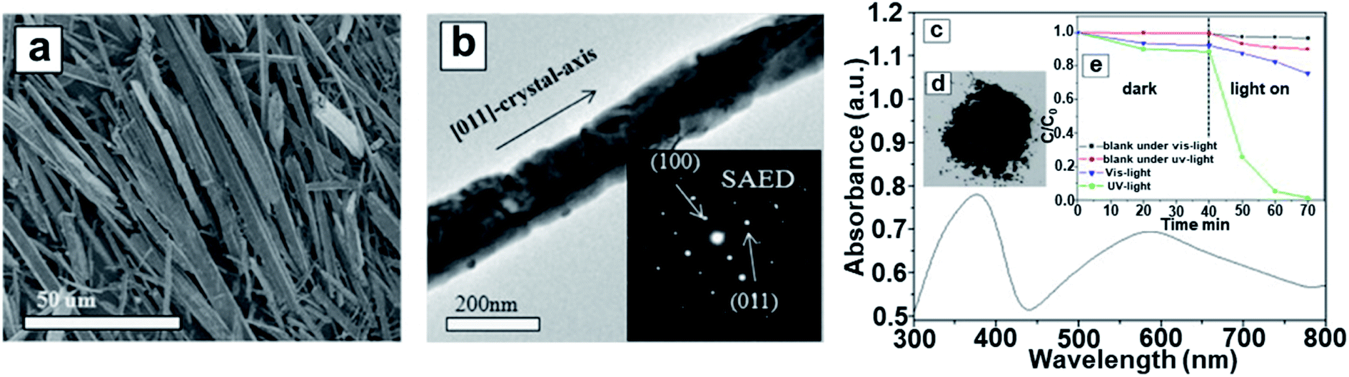 | ||
| Fig. 47 (a) FE-SEM and (b) TEM images of AgNbO3; (c) UV-visible diffuse reflectance spectra, (d) photographic image of AgNbO3 powder and (e) photocatalytic degradation of methylene bule (MB) by AgNbO3 nanostructures reported by Cao et al.209 [Reproduced with permission from ref. 209 copyright 2014 by Elsevier]. | ||
Lu et al.210 synthesized one-dimensional AgNbO3 using Ag nanowires as the raw material template. In contrast to the results reported by Cao et al., the final product was a one-dimensional nanostructured composite of Ag2Nb4O11 and AgNbO3, which showed an enhanced activity to degradation of 2,4-dichlorophene and rhodamine B (RhB). Most recently, Gao et al.211 synthesized submicron cubes of AgNbO3via hydrothermal treatment (HT) of Ag2O–Nb2O5–NH4HF2 aqueous suspensions, which exhibited excellent photocatalytic activity under visible-light irradiation (λ ≥ 400 nm) (see Fig. 48g). The microstructure analysis indicated that a (001) facet with high surface energy was exposed (see Fig. 48c and d). Further photoelectrochemical and photocatalytic performance analysis suggested that the cubes with an exposed (001) facet exhibit higher charge carrier separation efficiency with the greater redox ability of photogenerated electrons and holes being responsible for the superior photocatalytic activity.
 | ||
| Fig. 48 Field-emission scanning electron microscopy images of AgNbO3 (AN) prepared by (a) hydrothermal (HT) and (b) solid state (SSR) methods; (c) transmission electron microscopy image and (d) selected-area electron diffraction pattern of AN (HT); the insets in (b) and (c) show high-resolution transmission electron microscopy images of AN (SSR) and AN (HT), respectively; the inset in (d) shows the angle between the (020) and (110) facets in the AN (HT) cube; (e) UV-vis diffuse reflectance spectra of AN (HT) and AN (SSR); (f) transient photocurrent of AN (HT) and AN (SSR) irradiated with visible light (λ ≥ 400 nm); (g) specific photocatalytic activity of the catalysts. The inset in (g) shows repeated photocatalytic degradation of tetracycline in the presence of AN (HT) and nitrogen-doped TiO2, reported by Gao et al.211 [Reproduced with permission from ref. 211 copyright 2019 by Elsevier]. | ||
 | ||
| Fig. 49 (a) Schematic band structure (a1) and experimental photocatalytic performance (a2 and a3) of (AgNbO3)1−x(SrTiO3)x (ANST) solid-solution.212 [Reproduced with permission from ref. 212 copyright 2009 American Chemical Society]. The hybridization of the Ag 4d with O 2p lifts the top of the valence band. In the sample x = 0.25, both the conduction band and valence band are continuous. In the case of x = 0.95, discontinuous inter-bands (or doping levels) are formed by the small number of dopants. (b) Schematic band structure (b1)213 [reproduced with permission from ref. 213 copyright 2010 by Elsevier] and experimental photocatalytic performance (b2 and b3) [reproduced with permission from ref. 215 copyright 2007 by Elsevier] of (AgNbO3)1−x(NaNbO3)x (ANN) solid-solution.213,215 | ||
5.4 Composites possessing hetero-junction interfaces
The presence of interfaces in composite materials may bring an enhancement of photocatalytic activity. To date, several AgNbO3-based composites that show an enhancement of photocatalytic performance compared to the pristine bulk have been reported. Table 6 summarizes the photocatalytic properties of various AgNbO3-based composites. In AgBr/AgNbO3 composites, Wang et al.216 suggested that the enhancement of photocatalytic activity can be attributed to the AgBr/AgNbO3 heterostructure (formed at the interface), which creates an internal electric field, modulates the band structure, and favors an efficient separation of electrons and holes. Similar mechanisms have contributed to the enhanced photocatalytic activity of Ag2O/AgNbO3 p–n junctions as reported by Yang et al.217 Recently, Yu et al.218 synthesized an Ag/AgNbO3 plasmonic photocatalyst via a facile combustion method, obtaining a special porous nano-structure where high energy {001} and {220} facets were exposed (see Fig. 50). The authors believed that the enhanced photocatalytic efficiency is related to the synergy between surface plasmonic resonance (SPR), ferroelectric polarization, specific exposed crystal-facets and interfacial crystallinity.| Catalysts | Organics | UV/vis | Degrad./time (h) | k | Ref. |
|---|---|---|---|---|---|
| a RhB: rhodamine B; TC: tetracycline; MB: methylene blue. | |||||
| AgNbO3/AgSbO3 | RhB (2.5 mg L−1) | Vis | — | 0.02667 | 219 |
| Ag@AgCl/AgNbO3 | MB (10 mg L−1) | Vis | ∼65%/2 h | 0.007 | 220 |
| NiO/AgNbO3 | MB (10 mg L−1) | UV | ∼84%/3 h | — | 221 |
| AgBr/AgNbO3 | MB (10 mg L−1) | Vis | 74.62%/3 h | 0.0083 | 216 |
| Ag2O/AgNbO3 | RhB (10 mg L−1) | Vis | 95.4%/1.5 h | — | 217 |
| Ag/AgNbO3 | RhB (5 mg L−1) | — | — | 0.0447 | 218 |
| TC (10 mg L−1) | — | 70.2%/1 h | 0.0293 | ||
 | ||
| Fig. 50 (a) SEM image of Ag/AgNbO3 porous nano-structure, (b) enlargement of (a) with the structure model (the inset illustration) of the as-prepared particle; (c) typical HRTEM image of Ag/AgNbO3 porous nano-structure and the corresponding SAED pattern in (d); (e) HRTEM image of the prepared Ag/AgNbO3. (f) Schematic drawing illustrating the possible photocatalytic mechanism of the Ag/AgNbO3 plasmonic photocatalysts: (1) spatial separation of photo-generated carriers along the direction of potentials originating from ferroelectric polarization; (2) orientation transfer of photo-generated carriers onto {001} and {220} facets; (3) photo-generated electrons transfer from the {220} facets to Ag nanoparticles to reduce O2; (4) formation of free ˙OH via the reaction of ˙O2− with H2O; (5) formation of free ˙OH via the reaction of photo-generated holes with OH− in the solution; (6) rapid oxidation of RhB or (tetracycline)TC by free ˙OH.218 [Reproduced with permission from ref. 218 copyright 2019 by Elsevier]. | ||
6. Summary and outlook
In this review, progress in research on AgNbO3 and AgNbO3-based perovskites since their discovery in 1958 has been summarized. The review covers various aspects, from fundamental science to emerging applications, and allows us to draw some important conclusions in the following areas.6.1 Structures, polymorphic phases, and electric field-induced transitions
AgNbO3 is polymorphic and shows complex phase behavior, with intricate transformations induced by temperature variations and the application of an electric field. The M1 phase, stable up to ca. 70 °C, consists of an antiferroelectric-like matrix, in which ferroelectric clusters are locally present, which can successfully explain the non-linear polarization under weak and strong electric fields. Both structure and analysis of properties suggest that the dielectric anomaly denoted as (Tf) could originate from a phase transition associated with inversion symmetry. Electrical loading under high electric fields produces double polarization hysteresis loops, but the structure induced under high electric fields is still experimentally unknown. Future studies should be aimed at revealing the nature of the electric field-induced structure, by in situ diffraction techniques which have still not been carried out in this important material. Above the temperature Tf (∼170 °C in pure AgNbO3), the microstructures of both M2 (stable in the range of ∼70–270 °C) and M3 (stable in the range of ∼270–350 °C) phases still show the presence of polar clusters, but field-induced transformations are significantly suppressed and are difficult to drive, even at high electric fields. The frequency-independent diffuse dielectric anomaly near 270 °C is intimately related to the local disorder–order behavior of off-center cation displacements (especially Nb5+ ions) in the sub-lattice of its average AFE matrix. This emphasizes the importance of local structural heterogeneity at the sub-lattice scale to improve the dielectric response of a given material, especially at high frequency, and will guide the property optimization for specific applications, such as microwave capacitors.6.2 Effects of compositional modification
Chemical modifications by suitable elements can be guided by the perovskite tolerance factor and may result in the suppression of the local displacive behavior, as well as in an increased local structural disorder down to very low temperatures.Isovalent substitutions on the A-site, using Li, restrains antiferroelectricity and leads to the promotion of a ferroelectric-type order with rhombohedral structure possessing high piezoelectric, pyroelectric and fatigue performances. Gradual substitution of Ag+ with isovalent Na+ ions with a smaller radius than Ag+ allows for the formation of a perovskite solid solution and induces the crossover from double polarization hysteresis to ferroelectric-like loops. The presence of Na restricts the displacement of Nb5+ ions and suppresses the diffuse dielectric dispersion of AgNbO3. Additionally, the replacement of Ag+ by isovalent K+ has the effect of reducing antiferrodistortive instabilities and promotes ferroelectricity, characterized by orthorhombic symmetry and an emerging potential for explosive energy conversion due to the possibility of driving pressure-induced FE → AFE transitions.
A possible strategy to develop AgNbO3-based antiferroelectric solid-solutions is to substitute Ag+ with cations of different radius and valence, including bi- and tri-valent elements, such as Ca2+, Bi3+ and various rare-earth cations, which can provide chemical pressure to suppress ferroelectricity and increase the energy barrier between AFE and FE phases. Besides, the doping also creates defects and enhances local structural heterogeneity that can have negative impacts on the field-induced polar ordering. Similar effects can be obtained by the isovalent substitution of Nb5+ by Ta5+ on the B-site producing an increase in the characteristic fields EB and EF, and a decrease of the remnant polarization, with P–E loops tending to a linear shape with increasing Ta content, evidencing the stabilization of an antiferroelectric state.
6.3 Applications in dielectric energy storage
AgNbO3-based materials are promising lead-free candidates for energy storage capacitors, due to their large energy density values. These range from 2.1 J cm−3 in AgNbO3 to 6.3 J cm−3 in Ag(Nb0.45Ta0.55)O3 ceramics obtained at room temperature, attributed to the enhanced stability of antiferroelectricity and improved breakdown strength. Two methods can be used to further enhance Eb and are based on either intrinsic or extrinsic effects. One method consists of modulating the band structure and increasing the band gap to prevent the excitation of electrons from the valence band to the conduction band (intrinsic). The other method is based on reducing the grain size to increase the resistivity by increasing the amount of grain boundaries (extrinsic).One of the main issues that should be overcome in future research is to increase the energy storage efficiency, which is often lower than 70%. This can be achieved by reducing the hysteresis area of the polarization–electric field loop. Previous investigations on relaxor-ferroelectrics such as Pb(Mg1/3Nb2/3)O3 may provide guidance for designing the AgNbO3-based materials displaying field-induced reversible polar ordering with low hysteresis (i.e. ergodic relaxor-antiferroelectrics). Systematic studies combining experimental techniques and modelling should be able to provide improved compositional design criteria to obtain increased energy storage efficiency.
A better synergy between research groups in academia and companies engaged in the energy storage capacitor sector should be promoted to overcome additional technical issues that are currently preventing AgNbO3-based devices entering the energy storage market. These issues include the difficulties related to the processing of AgNbO3 in oxygen-rich environments with accurate temperature control and specific heat treatment schedules. Metallic Ag can easily form near the AgNbO3 surface when the oxygen content in the processing environment is not sufficient, inducing an n-type semiconductor state. Additionally, the cost of the Ag precursors and the compatibility with electrode materials are also important factors to consider in future development.
6.4 Applications in photocatalysis and photovoltaics
As a functional semiconductor, AgNbO3 is emerging not only as a potential photocatalyst for splitting water and degrading organic pollutants, but also as a photovoltaic material for solar-cells due to its narrow Eg, which can extend the absorption edge of the solar spectrum to the visible-light range, providing enhanced photocatalytic and photovoltaic performances. Theoretical calculations also suggest a narrower band gap (Eg ≈ 1.83 eV) compared to the reported experimental values (Eg ≈ 2.08–2.93 eV). This is attributed to the existence of unbonded Ag atoms and the Ag–O/Nb–O covalent bonds formed in the AgNbO3 lattice. The presence of metallic Ag is believed to be responsible for the surface plasmon resonance effect and for the observed extra visible-light absorption event and thus for ultimately enhancing the photocatalytic and photovoltaic performances. Furthermore, the visible-light photocatalytic activity can be tuned by the external voltage bias, which can modify the width of surface space charge regions (SCRs) in AgNbO3, allowing for the regulation of photocatalytic activity.To further improve the photocatalytic performance for specific applications, chemically-modified AgNbO3-based materials have been explored since 2006 according to the following three materials design strategies: (1) control of the nanostructured surface morphology by wet chemical methods to provide more reaction-sites; (2) change of the surface chemical potential by modulating the band structure to enhance redox reactions; and (3) introduction of heterogeneous interfaces to create an internal electric-field to promote the separation of photo-generated electron–hole pairs.
To date, rare studies have been carried out integrating two or three of these approaches to further improve the photocatalytic performance. In particular, AgNbO3-based ferroelectric materials would attract interest for photocatalytic application due to the large Ps coupled with the narrow Eg and SPR response. Besides AgNbO3-based ferroelectric photocatalysts, AgNbO3-based piezo- and pyro-electric semiconducting nanomaterials could also emerge as potential candidates for converting mechanical and thermal energy into chemical energy. Additionally, research focused on ferroelectric photocatalysis of AgNbO3 is still rare. However, previous studies reported intriguing photovoltaic properties found in electrically poled and mechanically polished AgNbO3 ceramics, which were proposed to originate from intrinsic FE polarization and strain gradient-induced flexoelectricity, respectively. At the same time, electrical poling and/or mechanical polishing can also cause the precipitation of metallic Ag from the lattice of AgNbO3 and change the surface electronic structure, such as the width of SCRs, influencing the photovoltaic properties. Therefore, more fundamental studies should be carried out in future to further understand the photovoltaic mechanism.
Conflicts of interest
There are no conflicts to declare.Acknowledgements
This work was supported by the National Natural Science Foundation of China (Grant No. 52072227), the Opening Project of the State Key Laboratory of High Performance Ceramics and Superfine Microstructures (Grant No. SKL202111SIC), the Postdoctoral Science Foundation of China (Grant No. 2019M653604), the Natural Science Pre-research Funding of Shaanxi University of Science & Technology (Grant No. 2020QNBJ-03), and The Royal Society (Newton Advanced Fellowship, Grant No. NAF\R1\201126).References
- X. H. Hao, J. W. Zhai, L. B. Kong and Z. K. Xu, Prog. Mater. Sci., 2014, 63, 1–57 CrossRef CAS.
- L. Jin, F. Li and S. J. Zhang, J. Am. Ceram. Soc., 2014, 97, 1–27 CrossRef CAS.
- H. R. Jo and C. S. Lynch, J. Appl. Phys., 2014, 116, 074107 CrossRef.
- Z. Liu, T. Lu, J. Ye, G. Wang, X. Dong, R. Withers and Y. Liu, Adv. Mater. Technol., 2018, 3, 1800111 CrossRef.
- H. Wang, Y. Liu, T. Yang and S. Zhang, Adv. Funct. Mater., 2019, 29, 1807321 CrossRef.
- Z. P. Gao, W. Peng, B. Chen, S. A. T. Redfern, K. Wang, B. J. Chu, Q. He, Y. Sun, X. F. Chen, H. C. Nie, W. Deng, L. K. Zhang, H. L. He, G. S. Wang and X. L. Dong, Phys. Rev. Mater., 2019, 3, 035401 CrossRef CAS.
- Y. J. Ji, Q. Li, F. P. Zhuo, Q. F. Yan, Y. L. Zhang and X. C. Chu, ACS Appl. Mater. Interfaces, 2019, 11, 32135–32143 CrossRef CAS PubMed.
- X. H. Hao and J. W. Zhai, Appl. Phys. Lett., 2014, 104, 022902 CrossRef.
- Q. F. Zhang, S. C. Chen, M. Y. Fan, S. L. Jiang, T. Q. Yang, J. F. Wang, G. Li and X. Yao, Mater. Res. Bull., 2012, 47, 4503–4509 CrossRef CAS.
- EU-Directive 2002/95/EC: Restriction of the Use of Certain Hazardous Substances in Electrical and Electronic Equipment (RoHS), Off. J. Eur. Union., 2003, 46, (L37), 19–23 Search PubMed.
- K. M. Rabe, in Functional Metal Oxides, 2013, pp. 221–244, DOI:10.1002/9783527654864.ch7.
- Y. T. G. Viola, C. Yu, Y. Tan, V. Koval, X. Wei, K. Choy and H. Yan, Prog. Mater. Sci., 2021, 122, 10083 CrossRef.
- D. Fu, M. Endo, H. Taniguchi, T. Taniyama and M. Itoh, Appl. Phys. Lett., 2007, 90, 252907 CrossRef.
- A. Kania, K. Roleder and M. Łukaszewski, Ferroelectrics, 1983, 52, 265–269 CrossRef.
- Y. Tian, L. Jin, H. F. Zhang, Z. Xu, X. Y. Wei, E. D. Politova, S. Y. Stefanovich, N. V. Tarakina, I. Abrahams and H. X. Yan, J. Mater. Chem. A, 2016, 4, 17279–17287 RSC.
- Y. Tian, J. Li, Q. Y. Hu, L. Jin, K. Yu, J. L. Li, E. D. Politova, S. Y. Stefanovich, Z. Xu and X. Y. Wei, J. Mater. Chem. C, 2019, 7, 1028–1034 RSC.
- N. N. Luo, K. Han, M. J. Cabral, X. Z. Liao, S. J. Zhang, C. Z. Liao, G. Z. Zhang, X. Y. Chen, Q. Feng, J. F. Li and Y. Z. Wei, Nat. Commun., 2020, 11, 4824 CrossRef CAS PubMed.
- T. Takeda, Y. Takahashi, N. Wada and Y. Sakabe, Jpn. J. Appl. Phys., 2003, 42, 6023 CrossRef CAS.
- M. Valant and D. Suvorov, J. Am. Ceram. Soc., 1999, 82, 88–93 CrossRef CAS.
- A. Fujishima and K. Honda, Nature, 1972, 238, 37–38 CrossRef CAS PubMed.
- H. Kato, H. Kobayashi and A. Kudo, J. Phys. Chem. B, 2002, 106, 12441–12447 CrossRef CAS.
- X. He, C. Chen, C. Li, H. Zeng and Z. Yi, Adv. Funct. Mater., 2019, 29, 1900918 CrossRef.
- N. Maso, D. I. Woodward, P. A. Thomas, A. Varez and A. R. West, J. Mater. Chem., 2011, 21, 2715–2722 RSC.
- P. Rozier and O. Szajwaj, J. Solid State Chem., 2008, 181, 228–234 CrossRef CAS.
- D. I. Woodward and R. Beanland, Inorg. Chem., 2014, 53, 8941–8948 CrossRef CAS PubMed.
- X. Liu, C. Qin, Y. Huang, L. Qin and H. J. Seo, J. Taiwan Inst. Chem. Eng., 2017, 78, 530–538 CrossRef CAS.
- Z. Chen, X. Cheng, W. Ye, R. Zheng, H. Zhu, H. Yu, N. Long, M. Shui and J. Shu, Chem. Eng. J., 2019, 366, 246–253 CrossRef CAS.
- M. Valant, A. K. Axelsson, B. Zou and N. Alford, J. Mater. Res., 2007, 22, 1650–1655 CrossRef CAS.
- H. B. Chang, M. Y. Shang, C. Y. Zhang, H. M. Yuan and S. H. Feng, J. Am. Ceram. Soc., 2012, 95, 3673–3677 CrossRef CAS.
- J. Wang, X. Wan, Y. Rao, L. Zhao and K. Zhu, J. Eur. Ceram. Soc., 2020, 40, 5589–5596 CrossRef CAS.
- M. B. Telli, Chemical solution deposition of silver tantalate niobate Ag(TaxNb1–x)O3 thin films, Doctoral Thesis, The Pennsylvania State University, 2005..
- A. Kania, J. Cryst. Growth, 1989, 96, 703–704 CrossRef CAS.
- M. Łukaszewski, A. Kania and A. Ratuszna, J. Cryst. Growth, 1980, 48, 493–495 CrossRef.
- W. Zhao, Z. Fu, J. Deng, S. Li, Y. Han, M.-R. Li, X. Wang and J. Hong, Chin. Phys. Lett., 2021, 38, 037701 CrossRef CAS.
- M. Francombe and B. Lewis, Acta Crystallogr., 1958, 11, 175–178 CrossRef CAS.
- Y. Lu, Q. Y. Shen, Q. N. Yu, F. Zhang, G. Q. Li and W. F. Zhang, J. Phys. Chem. C, 2016, 120, 28712–28716 CrossRef CAS.
- H. Moriwake, C. A. J. Fisher, A. Kuwabara and D. S. Fu, Jpn. J. Appl. Phys., 2013, 52, 09KF08 CrossRef.
- A. Kania, A. Niewiadomski, S. Miga, I. Jankowska-Sumara, M. Pawlik, Z. Ujma, J. Koperski and J. Suchanicz, J. Eur. Ceram. Soc., 2014, 34, 1761–1770 CrossRef CAS.
- Y. K. T. Egawa, Y. Noguchi and M. Miyayama, Jpn. J. Appl. Phys., 2016, 55, 10TB03 CrossRef.
- J. Li, Y. Tian, Y. Lan, L. Jin, C. Chen and X. Wei, Ceram. Int., 2021, 47, 26178–26184 CrossRef CAS.
- M. B. Telli, S. S. N. Bharadwaja, M. D. Biegalski, J. G. Cheng and S. Trolier-McKinstry, J. Appl. Phys., 2007, 101, 014111 CrossRef.
- J.-Y. Kim and A. M. Grishin, Thin Solid Films, 2006, 515, 615–618 CrossRef CAS.
- H. Sakurai, S. Yamazoe and T. Wada, Appl. Phys. Lett., 2010, 97, 042901 CrossRef.
- Y. Zhang, X. Li, J. Song, S. Zhang, J. Wang, X. Dai, B. Liu, G. Dong and L. Zhao, J. Materiomics, 2021, 7, 1294–1300 CrossRef.
- A. Kania and K. Roleder, Ferroelectr. Lett. Sect., 1984, 2, 51–54 CrossRef CAS.
- J. Fabry, Z. Zikmund, A. Kania and V. Petříček, Acta Crystallogr., Sect. C: Cryst. Struct. Commun., 2000, 56, 916–918 CrossRef PubMed.
- P. Sciau, A. Kania, B. Dkhil, E. Suard and A. Ratuszna, J. Phys.: Condens. Matter, 2004, 16, 2795 CrossRef CAS.
- I. Levin, V. Krayzman, J. C. Woicik, J. Karapetrova, T. Proffen, M. G. Tucker and I. M. Reaney, Phys. Rev. B: Condens. Matter Mater. Phys., 2009, 79, 104113 CrossRef.
- M. Yashima, S. Matsuyama, R. Sano, M. Itoh, K. Tsuda and D. S. Fu, Chem. Mater., 2011, 23, 1643–1645 CrossRef CAS.
- M. K. Niranjan and S. Asthana, Solid State Commun., 2012, 152, 1707–1710 CrossRef CAS.
- G. Li, H. Liu, L. Zhao, J. Gao, J. F. Li, R. Yu and J. Zhu, Appl. Phys. Lett., 2018, 113, 242901 CrossRef.
- U. Farid, A. S. Gibbs and B. J. Kennedy, Inorg. Chem., 2020, 59, 12595–12607 CrossRef CAS PubMed.
- T. Lu, Y. Tian, A. Studer, N. Narayanan, Q. Li, R. Withers, L. Jin, Y. Mendez-González, A. Peláiz-Barranco and D. Yu, IUCrJ, 2019, 6, 740–750 CrossRef CAS PubMed.
- A. Kania and J. Kwapulinski, J. Phys.: Condens. Matter, 1999, 11, 8933 CrossRef CAS.
- M. Pawełczyk, Phase Transitions, 1987, 8, 273–292 CrossRef.
- M. Verwerft, D. Van Dyck, V. Brabers, J. Van Landuyt and S. Amelinckx, Phys. Status Solidi A, 1989, 112, 451–466 CrossRef CAS.
- S. Miga and J. Dec, J. Appl. Phys., 1999, 85, 1756–1759 CrossRef CAS.
- A. Volkov, B. Gorshunov, G. Komandin, W. Fortin, G. Kugel, A. Kania and J. Grigas, J. Phys.: Condens. Matter, 1995, 7, 785 CrossRef CAS.
- W. Fortin, G. Kugel, J. Grigas and A. Kania, Ferroelectrics, 1996, 184, 273–276 CrossRef CAS.
- W. Fortin, G. Kugel, J. Grigas and A. Kania, J. Appl. Phys., 1996, 79, 4273–4282 CrossRef CAS.
- A. Kania, K. Roleder, G. Kugel and M. Fontana, J. Phys. C: Solid State Phys., 1986, 19, 9 CrossRef CAS.
- S. Miga, A. Kania and J. Dec, J. Phys.: Condens. Matter, 2011, 23, 155901 CrossRef CAS PubMed.
- M. Ivliev, S. Raevskaya, I. Raevskiĭ, V. Shuvaeva and I. Pirog, Phys. Solid State, 2007, 49, 769–779 CrossRef CAS.
- B. Zalar, A. Lebar, J. Seliger, R. Blinc, V. V. Laguta and M. Itoh, Phys. Rev. B: Condens. Matter Mater. Phys., 2005, 71, 064107 CrossRef.
- R. Blinc, Ferro-and Antiferroelectricity, 2007, pp. 51–67 Search PubMed.
- A. Levanyuk and D. G. Sannikov, Sov. Phys., Usp., 1974, 17, 199 CrossRef.
- Y. Yoneda, K. Yoshii and S. Kohara, Trans. Mater. Res. Soc. Jpn., 2012, 37, 73–76 CrossRef CAS.
- F. Cordero, Materials, 2015, 8, 8195–8245 CrossRef PubMed.
- D. Fu, M. Endo, H. Taniguchi, T. Taniyama, S.-y. Koshihara and M. Itoh, Appl. Phys. Lett., 2008, 92, 172905 CrossRef.
- T. Zhang, C. Zhang, L. Wang, Y. Chai, S. Shen, Y. Sun, H. Yuan and S. Feng, J. Am. Ceram. Soc., 2014, 97, 1895–1898 CrossRef CAS.
- H. Chang, M. Shang, C. Zhang, H. Yuan and S. Feng, J. Am. Ceram. Soc., 2012, 95, 3673–3677 CrossRef CAS.
- A. Kania and S. Miga, J. Am. Ceram. Soc., 2015, 98, 1040–1041 CrossRef CAS.
- V. Dvořák, Ferroelectrics, 1974, 7, 1–9 CrossRef.
- Z. Yan, D. Zhang, X. Zhou, M. Zhang, L. Zhang, H. Zhang, G. Xue, I. Abrahams and H. Yan, J. Mater. Chem. A, 2021, 9, 3520–3529 RSC.
- J. Gao, W. Li, J. Liu, Q. Li and J.-F. Li, Research, 2022, 2022, 9782343 CrossRef CAS PubMed.
- G. Li, H. Liu, L. Zhao, J. Gao, J.-F. Li and J. Zhu, J. Appl. Phys., 2022, 131, 124107 CrossRef CAS.
- H. Moriwake, A. Konishi, T. Ogawa, C. A. Fisher, A. Kuwabara, K. Shitara and D. Fu, Phys. Rev. B, 2018, 97, 224104 CrossRef CAS.
- Y. Tian, L. Jin, Q. Hu, K. Yu, Y. Zhuang, G. Viola, I. Abrahams, Z. Xu, X. Wei and H. Yan, J. Mater. Chem. A, 2019, 7, 834–842 RSC.
- W. Zhao, Z. Fu, J. Deng, S. Li, Y. Han, M.-R. Li, X. Wang and J. Hong, Chin. Phys. Lett., 2021, 38, 037701 CrossRef CAS.
- H. Moriwake, A. Konishi, T. Ogawa, C. A. Fisher, A. Kuwabara and D. Fu, J. Appl. Phys., 2016, 119, 064102 CrossRef.
- M. Yashima and S. Matsuyama, J. Phys. Chem. C, 2012, 116, 24902–24906 CrossRef CAS.
- G. Li, Y. Bai, X. Liu and W. Zhang, J. Phys. D: Appl. Phys., 2009, 42, 235503 CrossRef.
- F. Zhou, J. Zhu, Z. Lai, Y. Liu and X. Zhao, Appl. Phys. Lett., 2014, 105, 231121 CrossRef.
- S. Linic, P. Christopher and D. B. Ingram, Nat. Mater., 2011, 10, 911–921 CrossRef CAS PubMed.
- C. J. Bartel, C. Sutton, B. R. Goldsmith, R. Ouyang, C. B. Musgrave, L. M. Ghiringhelli and M. Scheffler, Sci. Adv., 2019, 5, eaav0693 CrossRef CAS PubMed.
- S. G. Kang, Int. J. Quantum Chem., 2017, 117, e25420 CrossRef.
- N. A. Benedek and C. J. Fennie, J. Phys. Chem. C, 2013, 117, 13339–13349 CrossRef CAS.
- J. Zhao, Etude théorique d'oxydes nano-structurés multifonctionnels, Université Sciences et Technologies – Bordeaux I, 2013, NT : 2013BOR14866 Search PubMed.
- M. Yashima and R. Ali, Solid State Ionics, 2009, 180, 120–126 CrossRef CAS.
- C. Shivakumara, Solid State Commun., 2006, 139, 165–169 CrossRef CAS.
- A. T. Mulder, N. A. Benedek, J. M. Rondinelli and C. J. Fennie, Adv. Funct. Mater., 2013, 23, 4810–4820 CAS.
- M. E. Lines and A. M. Glass, Principles and Applications of Ferroelectrics and Related Materials, Oxford University Press, New York, 1977 Search PubMed.
- N. A. Benedek, J. M. Rondinelli, H. Djani, P. Ghosez and P. Lightfoot, Dalton Trans., 2015, 44, 10543–10558 RSC.
- M. Kruczek, E. Talik and A. Kania, Solid State Commun., 2006, 137, 469–473 CrossRef CAS.
- R. Shannon, Acta Crystallogr., Sect. A: Cryst. Phys., Diffr., Theor. Gen. Crystallogr., 1976, 32, 751–767 CrossRef.
- S. Wada, A. Saito, T. Hoshina, H. Kakemoto, T. Tsurumi, C. Moriyoshi and Y. Kuroiwa, Jpn. J. Appl. Phys., 2006, 45, 7389 CrossRef CAS.
- A. Niewiadomski, D. Kajewski, A. Kania, K. Balin, S. Miga, M. Pawlik and J. Koperski, Ceram. Int., 2016, 42, 4445–4451 CrossRef CAS.
- D. I. Bilc and D. J. Singh, Phys. Rev. Lett., 2006, 96, 147602 CrossRef CAS PubMed.
- S. Wada, A. Saito, T. Hoshina, H. Kakemoto, T. Tsurumi, C. Moriyoshi and Y. Kuroiwa, Ferroelectrics, 2007, 346, 64–71 CrossRef CAS.
- A. Saito, S. Uraki, H. Kakemoto, T. Tsurumi and S. Wada, Mater. Sci. Eng., B, 2005, 120, 166–169 CrossRef.
- A. Kania and S. Miga, Mater. Sci. Eng., B, 2001, 86, 128–133 CrossRef.
- D. Fu, M. Endo, H. Taniguchi, T. Taniyama, M. Itoh and S.-y. Koshihara, J. Phys.: Condens. Matter, 2011, 23, 075901 CrossRef PubMed.
- H. Khan, I. Sterianou, S. Miao, J. Pokorny and I. Reaney, J. Appl. Phys., 2012, 111, 024107 CrossRef.
- Y. Yamamoto, I. Fujii and T. Wada, (Ag,Li)NbO3 thin films fabricated on (001), (110), and (111) SrTiO3 substrates by pulsed laser deposition, Joint IEEE International Symposium on Applications of Ferroelectric and Workshop on Piezoresponse Force Microscopy (ISAF/PFM), 2013, pp. 127–129, DOI:10.1109/ISAF.2013.6748673.
- Y. Guo, Y. Liu, R. L. Withers, F. Brink and H. Chen, Chem. Mater., 2011, 23, 219–228 CrossRef CAS.
- I. Levin and I. M. Reaney, Adv. Funct. Mater., 2012, 22, 3445–3452 CrossRef CAS.
- R. Garg, B. N. Rao, A. Senyshyn, P. Krishna and R. Ranjan, Phys. Rev. B: Condens. Matter Mater. Phys., 2013, 88, 014103 CrossRef.
- D. Kan, L. Pálová, V. Anbusathaiah, C. J. Cheng, S. Fujino, V. Nagarajan, K. M. Rabe and I. Takeuchi, Adv. Funct. Mater., 2010, 20, 1108–1115 CrossRef CAS.
- D. Kan, C. J. Long, C. Steinmetz, S. E. Lofland and I. Takeuchi, J. Mater. Res., 2012, 27, 2691 CrossRef CAS.
- T. Lu, Y. Tian, A. Studer, Q. Li, R. L. Withers, L. Jin, D. Yu, Z. Xu, X. Wei and Y. Liu, Chem. Mater., 2020, 32, 6456–6463 CrossRef CAS.
- S. Li, H. Nie, G. Wang, N. Liu, M. Zhou, F. Cao and X. Dong, J. Mater. Chem. C, 2019, 7, 4403–4414 RSC.
- Y. Kim, J. Kim, S. Yamanaka, A. Nakajima, T. Ogawa, T. Serizawa, H. Tanaka, M. Baba, T. Fukuda, K. Yoshii, M. Takeda, N. Yamada, T. Nakayama and K. Niihara, Adv. Energy Mater., 2015, 5, 1401942 CrossRef.
- M. E. Lines and A. M. Glass, Principles and Applications of Ferroelectrics and Related Materials, Oxford University Press, 2001 Search PubMed.
- D. Fu, M. Itoh and S.-y. Koshihara, J. Appl. Phys., 2009, 106, 104104 CrossRef.
- R. A. Klein, A. B. Altman, R. J. Saballos, J. P. S. Walsh, A. D. Tamerius, Y. Meng, D. Puggioni, S. D. Jacobsen, J. M. Rondinelli and D. E. Freedman, Phys. Rev. Mater., 2019, 3, 064411 CrossRef CAS.
- Y. Xu, G. Wang, Y. Tian, Y. Yan, X. Liu and Y. Feng, Ceram. Int., 2016, 42, 18791–18797 CrossRef CAS.
- Z. Liu, T. Lu, F. Xue, H. Nie, R. Withers, A. Studer, F. Kremer, N. Narayanan, X. Dong and D. Yu, Sci. Adv., 2020, 6, eaba0367 CrossRef CAS PubMed.
- H. D. Megaw, Ferroelectrics, 1974, 7, 87–89 CrossRef CAS.
- S. K. Mishra, N. Choudhury, S. L. Chaplot, P. S. R. Krishna and R. Mittal, Phys. Rev. B: Condens. Matter Mater. Phys., 2007, 76, 024110 CrossRef.
- A. Glazer and H. D. Megaw, Philos. Mag., 1972, 25, 1119–1135 CrossRef CAS.
- H. Z. Guo, H. Shimizu, Y. Mizuno and C. A. Randall, J. Appl. Phys., 2015, 117, 214103 CrossRef.
- H. Guo, H. Shimizu and C. A. Randall, J. Appl. Phys., 2015, 118, 174107 CrossRef.
- D. Fu, T. Arioka, H. Taniguchi, T. Taniyama and M. Itoh, Appl. Phys. Lett., 2011, 99, 012904 CrossRef.
- D. Klement, M. Spreitzer and D. Suvorov, J. Eur. Ceram. Soc., 2014, 34, 1537–1545 CrossRef CAS.
- M. Valant, D. Suvorov, C. Hoffmann and H. Sommariva, J. Eur. Ceram. Soc., 2001, 21, 2647–2651 CrossRef CAS.
- M. Valant, A.-K. Axelsson and N. Alford, J. Eur. Ceram. Soc., 2007, 27, 2549–2560 CrossRef CAS.
- H. P. Soon, H. Taniguchi and M. Itoh, Appl. Phys. Lett., 2009, 95, 242904 CrossRef.
- D. J. Singh, Phys. Rev. B: Condens. Matter Mater. Phys., 1996, 53, 176 CrossRef CAS PubMed.
- A. Kania, Phase Transit., 1983, 3, 131–139 CrossRef CAS.
- I. Levin, J. Woicik, A. Llobet, M. Tucker, V. Krayzman, J. Pokorny and I. Reaney, Chem. Mater., 2010, 22, 4987–4995 CrossRef CAS.
- L. Li, M. Spreitzer and D. Suvorov, Appl. Phys. Lett., 2014, 104, 182902 CrossRef.
- L. Zhao, Q. Liu, J. Gao, S. Zhang and J. F. Li, Adv. Mater., 2017, 29, 1701824 CrossRef PubMed.
- P. Iyer and A. Smith, Acta Crystallogr., 1967, 23, 740–746 CrossRef CAS.
- W. G. Mumme, I. E. Grey, B. Edwards, C. Turner, J. Nino and T. A. Vanderah, J. Solid State Chem., 2013, 200, 323–327 CrossRef CAS.
- Z. Zhang, C. J. Howard, B. J. Kennedy, K. S. Knight and Q. Zhou, J. Solid State Chem., 2007, 180, 1846–1851 CrossRef CAS.
- X. Hu, M. Valant and D. Suvorov, J. Appl. Phys., 2006, 99, 124109 CrossRef.
- Y. Tian, L. Jin, H. Zhang, Z. Xu, X. Wei, G. Viola, I. Abrahams and H. Yan, J. Mater. Chem. A, 2017, 5, 17525–17531 RSC.
- J. Gao, Q. Liu, J. Dong, X. Wang, S. Zhang and J.-F. Li, ACS Appl. Mater. Interfaces, 2020, 12, 6097–6104 CrossRef CAS PubMed.
- J. Gao, Y. Zhang, L. Zhao, K.-Y. Lee, Q. Liu, A. Studer, M. Hinterstein, S. Zhang and J.-F. Li, J. Mater. Chem. A, 2019, 7, 2225–2232 RSC.
- S. Li, H. Nie, G. Wang, C. Xu, N. Liu, M. Zhou, F. Cao and X. Dong, J. Mater. Chem. C, 2019, 7, 1551–1560 RSC.
- N. Luo, K. Han, F. Zhuo, C. Xu, G. Zhang, L. Liu, X. Chen, C. Hu, H. Zhou and Y. Wei, J. Mater. Chem. A, 2019, 7, 14118–14128 RSC.
- J. Gao, Y. C. Zhang, L. Zhao, K. Y. Lee, Q. Liu, A. Studer, M. Hinterstein, S. J. Zhang and J. F. Li, J. Mater. Chem. A, 2019, 7, 2225–2232 RSC.
- N. Luo, K. Han, F. Zhuo, L. Liu, X. Chen, B. Peng, X. Wang, Q. Feng and Y. Wei, J. Mater. Chem. C, 2019, 7, 4999–5008 RSC.
- Y. H. Xu, Y. Guo, Q. Liu, Y. H. Yin, J. L. Bai, L. Lin, J. J. Tian and Y. Tian, J. Alloys Compd., 2020, 821, 153260 CrossRef CAS.
- Y. H. Xu, Y. Guo, Q. Liu, G. D. Wang, J. L. Bai, J. J. Tian, L. Lin and Y. Tian, J. Eur. Ceram. Soc., 2020, 40, 56–62 CrossRef CAS.
- A. Song, J. Song, Y. Lv, L. Liang, J. Wang and L. Zhao, Mater. Lett., 2019, 237, 278–281 CrossRef CAS.
- Z. N. Yan, D. Zhang, X. F. Zhou, H. Qi, H. Luo, K. C. Zhou, I. Abrahams and H. X. Yan, J. Mater. Chem. A, 2019, 7, 10702–10711 RSC.
- L.-F. Zhu, L. Zhao, Y. Yan, H. Leng, X. Li, L.-Q. Cheng, X. Xiong and S. Priya, J. Mater. Chem. A, 2021, 9, 9655–9664 RSC.
- L. Zhao, J. Gao, Q. Liu, S. Zhang and J.-F. Li, ACS Appl. Mater. Interfaces, 2018, 10, 819–826 CrossRef CAS PubMed.
- L. Zhao, Q. Liu, S. J. Zhang and J. F. Li, J. Mater. Chem. C, 2016, 4, 8380–8384 RSC.
- N. Luo, K. Han, L. Liu, B. Peng, X. Wang, C. Hu, H. Zhou, Q. Feng, X. Chen and Y. Wei, J. Am. Ceram. Soc., 2019, 102, 4640–4647 CrossRef CAS.
- J. Li, L. Jin, Y. Tian, C. Chen, Y. Lan, Q. Hu, C. Li, X. Wei and H. Yan, J. Materiomics, 2022, 8, 266–273 CrossRef.
- P. Ren, D. Ren, L. Sun, F. Yan, S. Yang and G. Zhao, J. Eur. Ceram. Soc., 2020, 40, 4495–4502 CrossRef CAS.
- K. Han, N. Luo, S. Mao, F. Zhuo, L. Liu, B. Peng, X. Chen, C. Hu, H. Zhou and Y. Wei, J. Mater. Chem. A, 2019, 7, 26293–26301 RSC.
- Z. Lu, W. Bao, G. Wang, S.-K. Sun, L. Li, J. Li, H. Yang, H. Ji, A. Feteira, D. Li, F. Xu, A. K. Kleppe, D. Wang, S.-Y. Liu and I. M. Reaney, Nano Energy, 2021, 79, 105423 CrossRef CAS.
- W. Chao, J. Gao, T. Yang and Y. Li, J. Eur. Ceram. Soc., 2021, 41, 7670–7677 CrossRef CAS.
- W. Chao, T. Yang, Y. Li and Z. Liu, J. Am. Ceram. Soc., 2020, 103, 7283–7290 CrossRef CAS.
- Y. Xu, Z. Yang, K. Xu, Y. Cao, Y. Tian, L. Guo, J. Tian, H. Tian, X. Liu, L. Lin and G. Wang, Chem. Eng. J., 2021, 426, 131047 CrossRef CAS.
- L. Jin, J. Pang, R. Jing, Y. Lan, L. Wang, F. Li, Q. Hu, H. Du, D. Guo and X. Wei, J. Alloys Compd., 2019, 788, 1182–1192 CrossRef CAS.
- H. Borkar, V. Singh, B. Singh, M. Tomar, V. Gupta and A. Kumar, RSC Adv., 2014, 4, 22840–22847 RSC.
- J. Li, L. Zhang and S. Ducharme, Appl. Phys. Lett., 2007, 90, 132901 CrossRef.
- L. M. Wang, Relationship between Intrinsic Breakdown Field and Bandgap of Materials, 25th International Conference on Microelectronics, 2006, pp. 576–579, DOI:10.1109/ICMEL.2006.1651032.
- R. Gerson and T. C. Marshall, J. Appl. Phys., 1959, 30, 1650–1653 CrossRef CAS.
- A. Kishimoto, K. Koumoto, H. Yanagida and M. Nameki, Eng. Fract. Mech., 1991, 40, 927–930 CrossRef.
- T. Tunkasiri and G. Rujijanagul, J. Mater. Sci. Lett., 1996, 15, 1767–1769 CrossRef CAS.
- E. Beauchamp, J. Am. Ceram. Soc., 1971, 54, 484–487 CrossRef CAS.
- L. T. Yang, X. Kong, F. Li, H. Hao, Z. X. Cheng, H. X. Liu, J. F. Li and S. J. Zhang, Prog. Mater. Sci., 2019, 102, 72–108 CrossRef CAS.
- H. Y. Lee, K. H. Cho and H.-D. Nam, Ferroelectrics, 2006, 334, 165–169 CrossRef CAS.
- Z. Song, H. X. Liu, S. J. Zhang, Z. J. Wang, Y. T. Shi, H. Hao, M. H. Cao, Z. H. Yao and Z. Y. Yu, J. Eur. Ceram. Soc., 2014, 34, 1209–1217 CrossRef CAS.
- C. Neusel, H. Jelitto, D. Schmidt, R. Janssen, F. Felten and G. A. Schneider, J. Eur. Ceram. Soc., 2015, 35, 113–123 CrossRef CAS.
- G. Mazzanti, G.C. Montanari, F. Peruzzotti and A. Zaopo, Some remarks regarding the test cells used for electric strength measurements, IEEE International Symposium on Electrical Insulation, 1996, vol. 2, pp. 474–477, DOI:10.1109/ELINSL.1996.549385.
- H. Kim and F. Shi, IEEE Trans. Dielectr. Electr. Insul., 2001, 8, 248–252 CrossRef CAS.
- F. Bian, S. G. Yan, C. H. Xu, Z. Liu, X. F. Chen, C. L. Mao, F. Cao, J. J. Bian, G. S. Wang and X. L. Dong, J. Eur. Ceram. Soc., 2018, 38, 3170–3176 CrossRef CAS.
- K. Bi, M. H. Bi, Y. N. Hao, W. Luo, Z. M. Cai, X. H. Wang and Y. H. Huang, Nano Energy, 2018, 51, 513–523 CrossRef CAS.
- M. R. Hoffmann, S. T. Martin, W. Choi and D. W. Bahnemann, Chem. Rev., 1995, 95, 69–96 CrossRef CAS.
- A. Kudo and Y. Miseki, Chem. Soc. Rev., 2009, 38, 253–278 RSC.
- M. Grätzel, in Materials for Sustainable Energy: A Collection of Peer-Reviewed Research and Review Articles from Nature Publishing Group, World Scientific, 2011, pp. 26–32 Search PubMed.
- I. K. Konstantinou and T. A. Albanis, Appl. Catal., B, 2004, 49, 1–14 CrossRef CAS.
- D. Chatterjee and S. Dasgupta, J. Photochem. Photobiol., C, 2005, 6, 186–205 CrossRef CAS.
- L. Li, P. A. Salvador and G. S. Rohrer, Nanoscale, 2014, 6, 24–42 RSC.
- J. F. Reber and K. Meier, J. Phys. Chem., 1984, 88, 5903–5913 CrossRef CAS.
- O. Khaselev and J. A. Turner, Science, 1998, 280, 425–427 CrossRef CAS PubMed.
- J. Luo, J.-H. Im, M. T. Mayer, M. Schreier, M. K. Nazeeruddin, N.-G. Park, S. D. Tilley, H. J. Fan and M. Grätzel, Science, 2014, 345, 1593–1596 CrossRef CAS PubMed.
- L. Fang, L. You and J.-M. Liu, in Ferroelectric Materials for Energy Applications, 2018, pp. 265–309, DOI:10.1002/9783527807505.ch9.
- Z. Zhang, W. Wang, L. Wang and S. Sun, ACS Appl. Mater. Interfaces, 2012, 4, 593–597 CrossRef CAS PubMed.
- H. Razavi-Khosroshahi, K. Edalati, J. Wu, Y. Nakashima, M. Arita, Y. Ikoma, M. Sadakiyo, Y. Inagaki, A. Staykov and M. Yamauchi, J. Mater. Chem. A, 2017, 5, 20298–20303 RSC.
- R. B. Marcelino and C. C. Amorim, Environ. Sci. Pollut. Res., 2019, 26, 4155–4170 CrossRef PubMed.
- M. Kaneko and I. Okura, Photocatalysis: Science and Technology, Springer Berlin Heidelberg, 2002 Search PubMed.
- H. Wang, L. Zhang, Z. Chen, J. Hu, S. Li, Z. Wang, J. Liu and X. Wang, Chem. Soc. Rev., 2014, 43, 5234–5244 RSC.
- S. J. Moniz, S. A. Shevlin, D. J. Martin, Z.-X. Guo and J. Tang, Energy Environ. Sci., 2015, 8, 731–759 RSC.
- X. Wang and C. Li, J. Phys. Chem. C, 2018, 122, 21083–21096 CrossRef CAS.
- Y. Cui, J. Briscoe and S. Dunn, Chem. Mater., 2013, 25, 4215–4223 CrossRef CAS.
- M. Khan, M. Nadeem and H. Idriss, Surf. Sci. Rep., 2016, 71, 1–31 CrossRef CAS.
- W. Yang, B. Rodriguez, A. Gruverman and R. Nemanich, J. Phys.: Condens. Matter, 2005, 17, S1415 CrossRef CAS.
- P. M. Jones and S. Dunn, Nanotechnology, 2007, 18, 185702 CrossRef.
- W. Mönch, Electronic Properties of Semiconductor Interfaces, Springer Science & Business Media, 2013 Search PubMed.
- A. Bhardwaj, N. V. Burbure, A. Gamalski and G. S. Rohrer, Chem. Mater., 2010, 22, 3527–3534 CrossRef CAS.
- D. Tiwari and S. Dunn, J. Mater. Sci., 2009, 44, 5063–5079 CrossRef CAS.
- S. V. Kalinin, D. A. Bonnell, T. Alvarez, X. Lei, Z. Hu, J. Ferris, Q. Zhang and S. Dunn, Nano Lett., 2002, 2, 589–593 CrossRef CAS.
- G. Nataf, M. Guennou, J. Kreisel, P. Hicher, R. Haumont, O. Aktas, E. Salje, L. Tortech, C. Mathieu and D. Martinotti, Phys. Rev. Mater., 2017, 1, 074410 CrossRef.
- Y. Wang, M. Zhang, J. Liu, H. Zhang, F. Li, C. W. Tseng, B. Yang, G. Smith, J. Zhai and Z. Zhang, Adv. Energy Mater., 2020, 10, 2001802 CrossRef CAS.
- Y. Liu, S. Ye, H. Xie, J. Zhu, Q. Shi, N. Ta, R. Chen, Y. Gao, H. An and W. Nie, Adv. Mater., 2020, 32, 1906513 CrossRef CAS PubMed.
- E. K. Akdogan, C. J. Rawn, W. D. Porter, E. A. Payzant and A. Safari, J. Appl. Phys., 2005, 97, 084305 CrossRef.
- M. Yashima, T. Hoshina, D. Ishimura, S. Kobayashi, W. Nakamura, T. Tsurumi and S. Wada, J. Appl. Phys., 2005, 98, 014313 CrossRef.
- D. Arney, C. Hardy, B. Greve and P. A. Maggard, J. Photochem. Photobiol., A, 2010, 214, 54–60 CrossRef CAS.
- G. Li, S. Yan, Z. Wang, X. Wang, Z. Li, J. Ye and Z. Zou, Dalton Trans., 2009, 8519–8524 RSC.
- G. Li, T. Kako, D. Wang, Z. Zou and J. Ye, Dalton Trans., 2009, 2423–2427 RSC.
- W. Wang, J. Phys. Chem. Solids, 2011, 72, 1457–1461 CrossRef CAS.
- L. Cao, Z. Guo, J. Huang, C. Li, J. Fei, Q. Feng, P. Wen, Y. Sun and X. Kong, Mater. Lett., 2014, 137, 110–112 CrossRef CAS.
- Y. Lu, Q. Yu, F. Zhang, G. Li and W. Zhang, Appl. Phys. A, 2016, 122, 1–5 CrossRef CAS.
- B. Gao, D. Hu, C. Xiao, D. Li, B. Lin, Y. Chen and Y. Zheng, J. Phys. Chem. Solids, 2019, 135, 109083 CrossRef CAS.
- D. Wang, T. Kako and J. Ye, J. Phys. Chem. C, 2009, 113, 3785–3792 CrossRef CAS.
- G. Li, N. Yang, W. Wang and W. Zhang, Electrochim. Acta, 2010, 55, 7235–7239 CrossRef CAS.
- G. Li, Mater. Chem. Phys., 2010, 121, 42–46 CrossRef CAS.
- G. Li, T. Kako, D. Wang, Z. Zou and J. Ye, J. Solid State Chem., 2007, 180, 2845–2850 CrossRef CAS.
- C. Wang, J. Yan, X. Wu, Y. Song, G. Cai, H. Xu, J. Zhu and H. Li, Appl. Surf. Sci., 2013, 273, 159–166 CrossRef CAS.
- M. Yang, Y. Pu, W. Wang, J. Li, X. Guo, R. Shi and Y. Shi, J. Alloys Compd., 2019, 811, 151831 CrossRef CAS.
- Z. Yu, B. Zhan, B. Ge, Y. Zhu, Y. Dai, G. Zhou, F. Yu, P. Wang, B. Huang and J. Zhan, Appl. Surf. Sci., 2019, 488, 485–493 CrossRef CAS.
- G. Li, Y. Bai, W. Zhang and H. Zhang, Mater. Chem. Phys., 2013, 139, 1009–1013 CrossRef CAS.
- L. Yang, J. Liu, H. Chang and S. Tang, RSC Adv., 2015, 5, 59970–59975 RSC.
- H. Shu, J. Xie, H. Xu, H. Li, Z. Gu, G. Sun and Y. Xu, J. Alloys Compd., 2010, 496, 633–637 CrossRef CAS.
| This journal is © The Royal Society of Chemistry 2022 |