
 Open Access Article
 This Open Access Article is licensed under a
 Creative Commons Attribution 3.0 Unported Licence
Biaxially oriented silica–polypropylene nanocomposites for HVDC film capacitors: morphology-dielectric property relationships, and critical evaluation of the current progress and limitations†
Ilkka
Rytöluoto
 *a,
Minna
Niittymäki
b,
Paolo
Seri
c,
Hadi
Naderiallaf
c,
Kari
Lahti
b,
Eetta
Saarimäki
a,
Timo
Flyktman
a and
Mika
Paajanen
a
*a,
Minna
Niittymäki
b,
Paolo
Seri
c,
Hadi
Naderiallaf
c,
Kari
Lahti
b,
Eetta
Saarimäki
a,
Timo
Flyktman
a and
Mika
Paajanen
a
aVTT Technical Research Centre of Finland, Tampere, Finland. E-mail: ilkka.rytoluoto@vtt.fi
bLaboratory of Electrical Engineering, Tampere University, Tampere, Finland
cElectrical, Electronic and Information Engineering “Guglielmo Marconi” Dept., University of Bologna, Bologna, Italy
First published on 5th January 2022
Abstract
Dielectric polymer nanocomposites are considered as one of the most promising insulation material candidates for future capacitive energy storage applications, providing tailorability of charge trapping and transport properties at the nanometric level which is a key for increased dielectric performance of biaxially oriented polypropylene (BOPP) for metallized film capacitors in high-voltage direct current (HVDC) applications. In this study, a comprehensive investigation of morphology and dielectric performance of pilot-scale BOPP nanocomposites with hexamethyldisilazane (HMDS)-treated hydrophobic fumed silica nanoparticles was carried out, providing critical perspectives on the performance and challenges of PNCs for thin film capacitors also in a broader context. In non-oriented cast films, incorporation of nanosilica modified the crystallization kinetics and α/β-crystalline spherulitic morphology of polypropylene and reduced the accumulation of space charge under a DC electric field. The nanocomposites exhibited promising dispersion characteristics in the nano-scale, however, the low amount of micron-sized agglomerates inherently present in commercial fumed silica persisted in the compounds which can become critical for thin film applications. Subsequently, biaxial-stretching-induced morphology development and dielectric properties of silica-BOPP nanocomposites were evaluated, highlighting the role of precursor morphology and film processing in the silica-BOPP film morphology, defects and dielectric performance. Charge trapping and transport properties of silica-BOPP films were investigated by isothermal and thermally stimulated techniques under high DC electro-thermal stresses, indicating profound modification of the trap density of states brought about by nanosilica. This resulted in more homogeneous space charge distribution and reduced temperature- and field dependent DC conductivity at 100 °C in comparison to neat BOPP under moderate field stresses (<200 V μm−1), while simultaneously maintaining low dielectric loss. However, the localized weak points caused by silica agglomerates still remain a challenge for the structural homogeneity and dielectric breakdown performance of thin BOPP films under extreme-field stress, hence emphasizing the need for further advancements in the agglomerate and PNC film morphology control to provide high-reliability nanodielectric capacitor thin films for practical HVDC film capacitor applications.
Introduction
Biaxially oriented polypropylene (BOPP) film is the de facto industry standard for the main insulation layer in current state-of-the-art polymer film capacitors employed in various demanding HVDC applications such as voltage source converters (VSC) with scalable modular multi-level converter (MMC)-topography for grid-interfacing of renewable energy sources to the hybrid AC/DC power grids.1,2 Modern BOPP capacitor films—being produced from the highest purity capacitor-grade isotactic PP resins by the sequential tenter film process3,4—exhibit several key performance characteristics such as ultra-low dielectric loss characteristics2,5 (tan![[thin space (1/6-em)]](https://www.rsc.org/images/entities/char_2009.gif) δ in the range of 10−4), high specific capacitance for film thicknesses6 reaching as low as 1.9 μm, low DC conductivity (less than 10−16 S m−1 at 70 °C, independent of electric field up to 200 VDC μm−1),2,7 excellent short-term dielectric breakdown strength (up to 769 VDC μm−1 at room temperature for large film areas),2,8 and graceful ageing characteristics due to excellent self-clearing breakdown capability in metallized form.9,10 Nevertheless, under high electro-thermal stresses encountered in modern-day HVDC power capacitor applications where nominal operation electric field and maximum temperature stresses can reach up to >200 VDC μm−1 and >105 °C,11 respectively, the dielectric performance and reliability of BOPP thin film insulation are significantly reduced as the material approaches its natural limits.12 Under such high stresses, several issues including space charge accumulation,13 ageing,14 non-linear conductivity increase and accelerated degradation,15,16 increased dielectric loss17 and capacitance loss due to increased probability of breakdown18,19 begin to compromise the dielectric integrity and lifetime of BOPP. This necessitates voltage de-rating at high temperatures or the use of auxiliary cooling systems for modern BOPP metallized film capacitors,10,18 hence reducing the capacitor energy density below the current industrial needs for demanding applications where significant heat is inherently present and the permitted volume and mass of capacitor units are limited (such as in off-shore HVDC converter stations and power electronic inverters for electric vehicles10). Therefore, new innovations towards enhancing the electro-thermal insulation performance of BOPP capacitor films beyond the current-state-of-the art—while simultaneously maintaining high insulation reliability for critical capacitor applications where the expected lifetime can be several tens of years20—are actively sought after.
δ in the range of 10−4), high specific capacitance for film thicknesses6 reaching as low as 1.9 μm, low DC conductivity (less than 10−16 S m−1 at 70 °C, independent of electric field up to 200 VDC μm−1),2,7 excellent short-term dielectric breakdown strength (up to 769 VDC μm−1 at room temperature for large film areas),2,8 and graceful ageing characteristics due to excellent self-clearing breakdown capability in metallized form.9,10 Nevertheless, under high electro-thermal stresses encountered in modern-day HVDC power capacitor applications where nominal operation electric field and maximum temperature stresses can reach up to >200 VDC μm−1 and >105 °C,11 respectively, the dielectric performance and reliability of BOPP thin film insulation are significantly reduced as the material approaches its natural limits.12 Under such high stresses, several issues including space charge accumulation,13 ageing,14 non-linear conductivity increase and accelerated degradation,15,16 increased dielectric loss17 and capacitance loss due to increased probability of breakdown18,19 begin to compromise the dielectric integrity and lifetime of BOPP. This necessitates voltage de-rating at high temperatures or the use of auxiliary cooling systems for modern BOPP metallized film capacitors,10,18 hence reducing the capacitor energy density below the current industrial needs for demanding applications where significant heat is inherently present and the permitted volume and mass of capacitor units are limited (such as in off-shore HVDC converter stations and power electronic inverters for electric vehicles10). Therefore, new innovations towards enhancing the electro-thermal insulation performance of BOPP capacitor films beyond the current-state-of-the art—while simultaneously maintaining high insulation reliability for critical capacitor applications where the expected lifetime can be several tens of years20—are actively sought after.
Background – progress of BOPP-nanocomposites towards film capacitor applications
Fundamentally, the DC electro-thermal properties of BOPP are trap-controlled—that is, the electronic trap states within the energy band gap of semi-crystalline PP arising from physical/morphological disorder3,21 and chemical defects22 dictate the temperature- and field-dependent mobility, trapping and scattering of free charge carriers. The nature of these electron/hole trap states, particularly the trap density and depth distribution (both energetic and spatial), has significant effects on the bulk polarization, electrical conductivity, space charge accumulation and dielectric strength of polymer insulation, thus making it very desirable to be able to control their nature and quantity. In this context, dielectric polymer nanocomposites (PNC) have been considered as one of the most potential material candidates for future electric energy storage applications, providing tailorability of the dielectric properties at the nanometric level.23 Essentially, due to the enormous surface-to-volume ratio of nanoparticles (NP), the vast interface between the polymeric host and the nanoparticles provides a unique route to locally alter charge trapping and transport properties, which, in well-dispersed PNC systems, can be reflected as a beneficial modification of the bulk dielectric properties. Good dispersion of nanoparticles, compatibility with the polymeric host, and avoidance of large agglomerates which can act as electrical weak points are among the key pre-requisites for high-performance nanocomposite dielectrics. Surface functionalization of the nanoparticles by organic modifiers such as silanes plays an essential role in enhancing the NP dispersion and compatibility with the polymeric host, and in modifying the electrical properties at the NP–matrix interface via introduction of electro-active chemical groups which constitute to the formation of new localized charge trapping sites with designed trap properties.24–26Considering recent studies on PP-based nanocomposites aimed for film capacitor applications, two principal nanocomposite strategies have gained high interest, namely (i) increasing the composite permittivity via inclusion of high-permittivity nanoparticles, or (ii) increasing the maximum permissible operation field strength by nanostructuration (by increasing operation voltage or, conversely, by reducing the film thickness). These two approaches are motivated primarily by the potential increase obtainable in capacitor energy density: for linear dielectrics (such as BOPP), the volumetric energy density of the dielectric film layer is governed by the equation u = 1/2εrε0E2 where εr is the (temperature-dependent) relative permittivity, ε0 is the vacuum permittivity and E is the electric field strength. The former approach, focusing on enhancing the effective dielectric permittivity, is however challenging,27 as high volume fraction (near or above percolation) of high-permittivity fillers such as BaTiO3 is needed to realize any appreciable increase in PP-nanocomposite permittivity,28 leading simultaneously to unfavourable electric field enhancement and increased breakdown probability in the polymer matrix, unacceptably high interfacial polarization loss and poor tensile strength which is critical for industrial film manufacturing.29,30 On the other hand, the latter approach, focusing on increasing the maximum permissible electric field stress of PP films via inclusion of permittivity-matching nanoparticles to tailor the charge trapping and transport properties at the nanometric level, has been shown to be a promising route towards practical film capacitor applications. Previously, pathways to the modification of the trap density of states and indications of bulk dielectric property improvement in BOPP films through incorporation of low amounts of surface-functionalized inorganic nanoparticles such as SiO2, Al2O3, TiO2 and POSS have been demonstrated,31–33 including decreased electrical conductivity and space charge accumulation,34–36 increased short-term dielectric breakdown strength,33,37,38 and increased resistance against partial discharges (PD),38 for instance.
However, assessing the performance of new (nano-) dielectrics for film capacitor applications necessitates careful testing of the properties in relevant morphologies and thickness scales, i.e. in biaxially stretched films, as a first step. Especially for very thin capacitor films (5 μm or less), avoiding structural inhomogeneities caused by e.g. NP agglomeration and cavitation/void formation during biaxial stretching, or other manufacturing issues such as inhomogeneous film thickness and surface texture, pinholes, wrinkles etc. is imperative for ensuring good industrial processability and high dielectric performance.23,39 This information cannot be obtained directly from laboratory-scale prototypical PNC specimens (e.g. hot-pressed or solvent-cast films), but instead, it necessitates careful investigation and optimization of the PNC composition, compounding, morphology formation and processing into biaxially oriented thin films using industrially relevant manufacturing methods (i.e. melt extrusion and biaxial orientation). This has been seldomly reported in a comprehensive manner,37,39,40 thus leaving processing–structure–property relationships in BOPP nanocomposites largely non-established. Moreover, understanding the fundamental mechanisms for dielectric property enhancement as well as the current limiting factors for biaxially oriented PNC thin films is highly required for advancing the field.39 Thereafter, bridging the gap between laboratory studies on prototypical samples and industrial scale capacitor film processing by film scale-up is a necessity, followed by component level studies (in actual capacitors or elements) where the evaluation of performance at relevant scales of capacitor film area (up to 1000 m2 in large capacitor banks), electro-thermal stress (>200 V μm−1 at ∼70–85 °C) and operation time (up to tens of years) can be approached by accelerated tests.11,18
This study focuses especially in the first part, i.e. to provide detailed information about the processing–structure–property relationships and underlying mechanisms for pilot-scale BOPP PNC films filled with hydrophobic fumed silica nanoparticles (the latter part, focusing on film scale-up and capacitor level tests will be presented elsewhere). In this study, pilot-scale PP nanocomposite films incorporating hydrophobic fumed silica nanoparticles were prepared via industrially relevant melt-blending, film extrusion and biaxial stretching approach. Several pilot-scale compounding and film processing trials were performed over the course of four years during which processing and film morphology were investigated and subsequently improved. Thus, more than 25 different silica–PP nanocompounds and non-oriented/biaxially oriented film variants with different compositions, compounding parameters and film processing are considered. Detailed analysis and critical evaluation of morphology, silica dispersion, biaxially stretched film structure formation and dielectric properties of silica–PP nanocomposites are presented, and potential for future film capacitor applications are discussed.
Experimental
Materials and film processing
Compounds comprising a capacitor-grade isotactic polypropylene (iPP) homopolymer matrix and 0–4.5 wt% of commercial hydrophobic fumed silica nanoparticles (Evonik Aerosil® R 812 S) after-treated with hexamethyldisilazane (HMDS) were manufactured. Standard phenolic antioxidant (AO) was added at two different concentrations for preventing thermo-oxidative degradation of the PP matrix during the melt processing (the exact concentrations are not given here, however, the relative amounts were high-AO [wt%] > low-AO [wt%]). The naming convention used in this study is PP-[silica content]-[antioxidant content]-[masterbatch route], e.g. PP-1.0-HighAO-MB1 refers to a 1.0 wt% silica PP composite with a high antioxidant content prepared via masterbatch route (explained below).Pre-mixed and dried raw materials were compounded using a KraussMaffei Berstorff ZE 25 × 49D UTX compounder with nitrogen gas purge and a screen pack (screw speed 150 rpm, output 7–18 kg h−1, up to >1000 kg production batches). The screw geometry was optimized for highly dispersive mixing of nanoparticles. The compounded strands were cooled in filtered water bath, pelletized and then extruded into ∼350–400 μm thick cast films using a Brabender Plasticorder single screw extruder inside a mobile soft-walled clean room (temperature profile of 200–230 °C, screw speed of 70–80 rpm, 18 μm screen pack for filtering of large agglomerates). While most of the compounds were manufactured by direct mixing, additional 1.0 wt% PP–silica compounds were also prepared by diluting 4.5 wt% silica–PP masterbatch with virgin PP either by twin-screw compounder (MB1) or during the cast film extrusion (MB2). The masterbatch route is relevant especially from the perspective of up-scaling the production process to industry level, and for possible reduction of nanosilica agglomerate size and quantity by the additional melt-mixing and filtration taking place during the dilution of the masterbatch. Finally, 10 cm × 10 cm specimens cut from the cast films were biaxially stretched into thin films inside a semi-clean room using a Brückner KARO IV laboratory stretcher. Biaxial stretching parameters were varied (stretching temperature ∼153–163 °C, pre-heating time 60–120 s, stretching speed 417% per s, simultaneous biaxial stretch ratio up to 6.0 × 6.0) with the resulting silica-BOPP film thicknesses being in the ∼5–12 μm range.
Morphological characterization
 | (1) |
41). Two parallel specimens were measured for each compound. The realized nanoparticle weight fractions (φ) in the nanocompounds were determined from cast film samples by burning the organic polymer and additives at 600 °C and weighing the residual ash in accordance with the ISO 3451-1 standard. The realized nanoparticle concentrations obtained by the ash method are typically slightly lower than the targeted concentrations,33,37 being attributable to rate fluctuations and loss in the gravimetric feeding of low amounts of nanosilica during compounding.
Non-isothermal crystallization kinetics of cast film specimens were studied by dynamic DSC scans in the −50 °C to 230 °C temperature range by varying cooling rates of 2.5, 5, 10 and 20 °C min−1. Relative degree of crystallinity as a function of temperature was calculated for each cooling rate from the corresponding dynamic crystallization exotherms as:
 | (2) |
 was measured using a Novocontrol Alpha-A dielectric analyzer equipped with a Novocool temperature control system in the 0.01 Hz to 1 MHz frequency range. Temperature dependence of the complex dielectric permittivity was studied in the −60 °C to +120 °C temperature range.
Thermally stimulated polarization and depolarization current measurements (TSDC/TSPC) and isothermal charging/discharging current measurements (ICC/IDC) were performed by using a custom-built modular test setup comprising of a high voltage DC source (Keithley 2290E-5), a sensitive electrometer (Keithley 6517B) and a temperature control unit (Novocool). A shielded thin film sample cell equipped with a PT100 temperature sensor (Novocontrol BDS1200 HV sample cell) and shielded cables were used for all the measurements. Temperature control (accuracy of ±0.1 °C) was realized using the Novocool system (TSDC/TSPC measurement) or a PID-controlled electrical heating element (ICC/IDC measurement). A diode-based overload protection circuit and a 100 kΩ series resistor were used to protect the electrometer in case of a sample breakdown during high voltage application. The charging/discharging current was recorded for the whole duration of the TSDC/TSPC measurement, yielding also information about the transient conductivity characteristics under isothermal mode (charging phase prior to TSDC measurement).
Results and discussion
Cast film properties
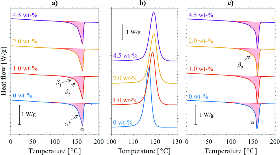 | ||
| Fig. 1 DSC data of selected PP–silica cast films: (a) First heating (initial cast film morphology), (b) first cooling (crystallization from melt) and (c) second heating. The curves are offset in y-direction for clarity and melting peaks corresponding to α- and β-form crystallinity are labelled. | ||
While the overlapping α/β-form melting/crystallization/re-melting processes occurring during the DSC heating scan complicate the accurate determination of the crystallinity of the original (cast film) state,47 the degree of crystallinity can nevertheless be estimated from the melting enthalpies by eqn (1) to evaluate the effect of nanosilica, see Table S1.† A slightly decreasing trend in cast film XDSC with increasing silica content was observed both for the first and second heating endotherms (measurement uncertainty in degree of crystallinity was ±0.2%), indicating a subtle modification of the crystallization behavior of PP brought by nanosilica. This is further supported by the increase (and saturation) of the crystallization peak temperature with increasing silica content during cooling from the melt (Fig. 1b), being attributable to a mild increase in nucleation density upon incorporation of hydrophobic silica NPs.48–50
The small increase in nucleation density can be related with the slightly higher propensity for β-phase formation for the silica–PP nanocompounds in comparison to neat PP, which is clearly seen especially in the second heating endotherms (Fig. 1c). In other words, when the crystallization conditions are suitable for β-crystal growth (generally in temperature range of 90–130 °C), as is the case for the relatively slow DSC cooling as opposed to the rapid cooling during cast film extrusion, nanosilica can promote β-crystal formation. This was visually confirmed by cross-sectional POM analysis of the cast films (see Fig. S1a and b†), showing spherulitic skin-core-type morphologies with slightly higher amount of (birefringent) β-spherulites observable for the silica-containing cast films. The nanosilica-induced changes in β-crystallinity are however considered minor and they can be likely compensated by fine-tuning of the cast film extrusion parameters (most importantly the cooling gradient). This is important, as excessive β-crystal content in the core layers of capacitor cast film can lead to porosity and void formation upon biaxial stretching, hence reducing the dielectric breakdown strength.43 We note here several recent studies, aimed for capacitor applications, where the beneficial role of crystallization conditions51 or nucleating additives (e.g. β-nucleating agents52–54) are highlighted for controlling the density and nature of the crystalline–amorphous interface and improving dielectric properties of PP. However, it is important to consider that during biaxial stretching of PP—a critical conversion step to obtain thin high-performance BOPP dielectric film43,55—biaxial-stretching-induced transformation of the mixed α/β-spherulitic precursor film morphology into a complex BOPP fibrillar morphology with predominantly α-crystalline structure occurs, and thus it is not always straightforward to relate the effects of crystalline modification on prototypical PP specimens with BOPP film properties.
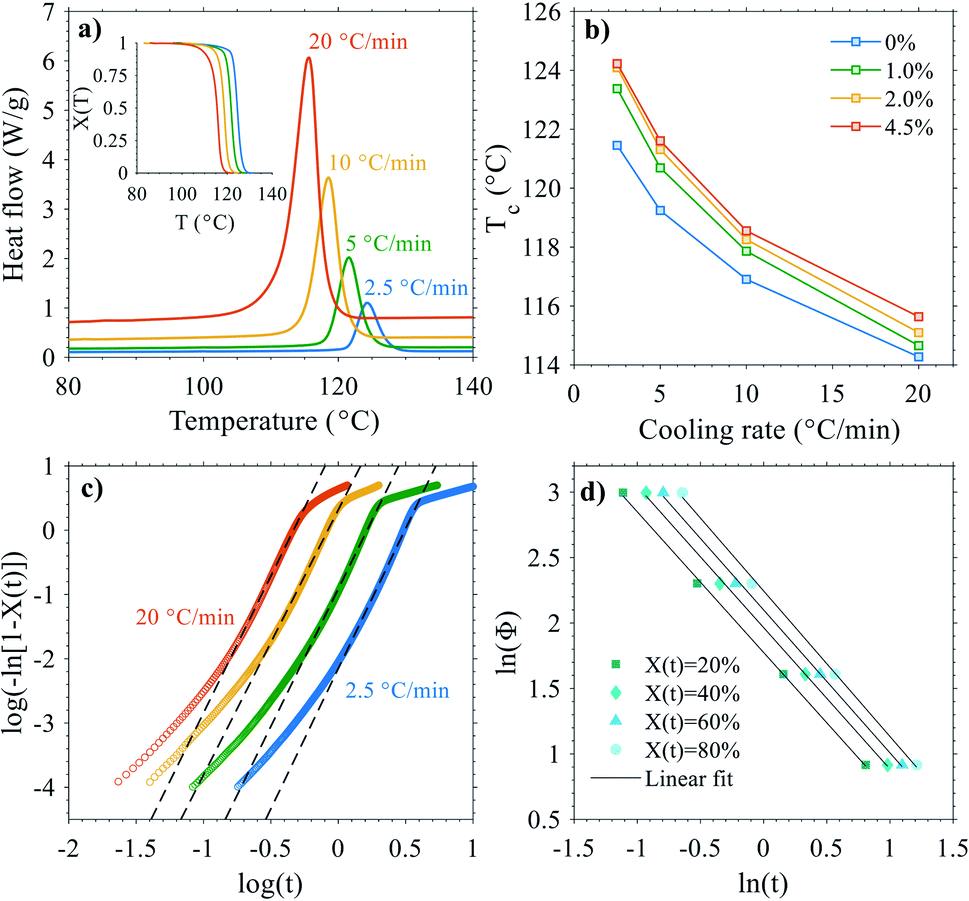 | ||
| Fig. 2 a) DSC crystallization exotherms under various cooling rates for PP-4.5-HighAO. The inset shows the relative degree of crystallinity X(T). (b) Dependence of the crystallization peak temperature Tc on the cooling rate for 0–4.5 wt% silica composites. (c) is the Avrami analysis plot and (d) is the combined Ozawa–Avrami plot for 4.5 wt% silica–PP composite. | ||
Due to the inadequacy of the Avrami model to fully describe the non-isothermal crystallization, further analysis was carried out based on the combined Ozawa–Avrami model which has been proven to be well-applicable for describing non-isothermal crystallization process.60 Exemplifying Ozawa–Avrami plots of a 4.5 wt% silica–PP composite are presented in Fig. 2d. Good linear correlation was observed for all the studied compounds (mean R2 of 0.998), indicating that the combined Ozawa–Avrami model can describe the non-isothermal crystallization process in the studied compounds satisfactorily. The derived Ozawa–Avrami parameters are listed in Table S2.† At a given degree of crystallinity, an increase in F(T) was systematically observed for the silica nanocomposites in comparison to neat PP, i.e. higher cooling rate is needed within unit crystallization time: this indicates that the rate of crystallization in PP is decreased with increasing nanosilica content, being consistent with the implications from the modified Avrami model analysis above. This implication of reduced crystallization rate brought by HMDS-treated nanosilica for the samples studied herein is in contrast with the data presented previously e.g. for isotactic PP composites with dimethyldichlorosilane (DDS)-treated hydrophobic fumed nanosilica (Aerosil® R974).56 The reduced crystallization rate for the samples herein may however be related to the degree (quality) of silica dispersion and inter-particle distance in the PP matrix, as besides nucleation, well-dispersed nanosilica particles can also confine the crystallizable matter into more restricted space and reduce the mobility of crystallizing units, hence hindering the (spherulite) growth rate.48
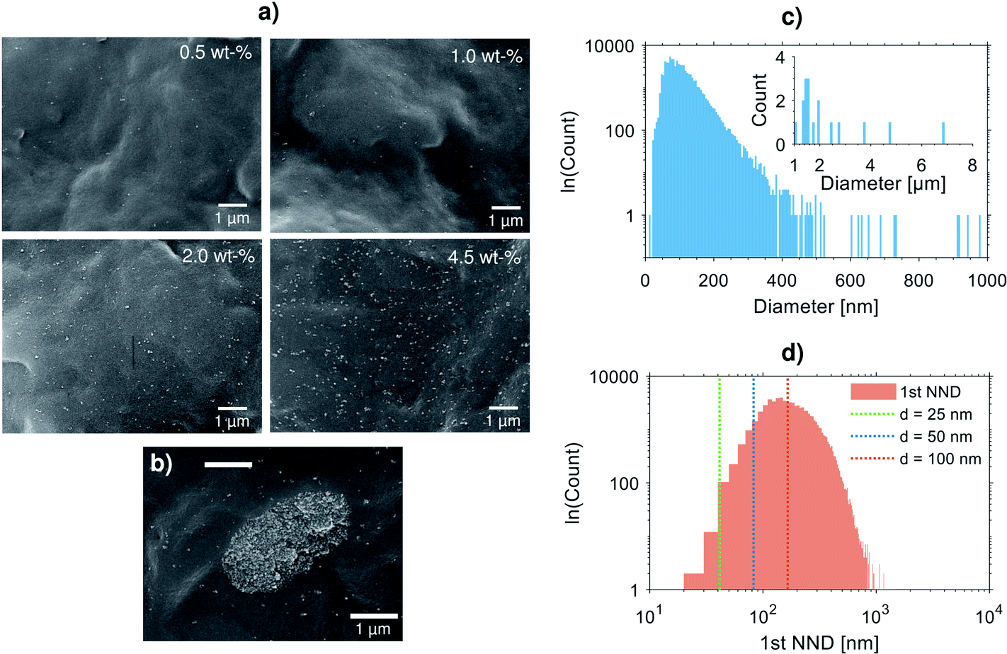 | ||
| Fig. 3 a) Representative SEM micrographs of 0.5–4.5 wt% silica–PP nanocomposites (high AO content, direct mixing). (b) Example of a large silica micro-agglomerate encountered in a 2.0 wt% silica–PP composite. The histograms in (c) and (d) present the quantitative particle size and 1st nearest neighbour distance (1st NND, center-to-center) statistics of PP-4.5-HighAO composite, respectively, as determined from 83 SEM micrographs (total image area ∼12796 μm2). The inset in (c) shows a close-up view of the right-hand tail of the histogram (μm-sized agglomerates). In (c), the vertical dashed lines are the theoretical 1st NND values of ideal 3D-monodispersions of 4.5 wt% of spherical particles with varying particle diameter. | ||
For statistical analysis of the dispersion, distribution and size of the silica particles, quantitative batch analysis of a large array of over 80 SEM images taken from PP-4.5-HighAO compound was carried out. The silica diameter histogram for the 4.5 wt% composite shown in Fig. 3c exhibits a right-skewed distribution shape similar to log-normal distribution with mean = 102.8 nm, median = 92.6 nm and mode = 57.2 nm. However, although these basic statistics are quite encouraging in the context of nanodielectrics, the right tail of the particle size distribution implies that there is still a need for dispersion improvement. Indeed, large micron-sized agglomerates—although relatively scarce in quantity within the studied sample area as shown in the inset of Fig. 3c—can sum up to significant density in large scale relevant to capacitor dielectric film area (up to several hundreds of m2) which can lead to cavitation or film breakage during biaxial stretching and can deteriorate the local dielectric strength of the film. One such agglomerate with a diameter of ∼3 μm is exemplified in Fig. 3b, and it is comprised of numerous closely-packed silica aggregates. The micron-sized agglomerates are suspected to originate from the production of fumed silica and subsequent hydrophobization by silane surface treatment, and despite several attempts to promote de-agglomeration during compounding by e.g. high-shear mixing, extensional flow mixing, repeated compounding cycles and melt-filtering it was not possible to completely eliminate them from the nanocompounds. Although the self-healing breakdown capability of metallized films can, to some extent, remedy the situation by isolating such local weak points in capacitor film application, the results point towards advancements in nanosilica de-agglomeration and dispersion being critical in order to avoid compromising film capacitor reliability and lifetime.14
On the other hand, under medium electrical–thermal stresses within the continuous operation stress regime where the breakdown probability is lower, inter-particle distance (IPD) has been shown to play a major role in charge trapping and transport properties which dictate conductivity and space charge accumulation.62 To support the above dispersion analysis, first nearest neighbour distance (1st NND) statistics were determined for the 4.5 wt% silica–PP composite data (Fig. 3d), providing a measure of the silica distribution and IPD variation. The average nearest-neighbour separation in a random 2D plane section through 3D array of uniformly distributed spherical particles can be estimated as:63
 | (3) |
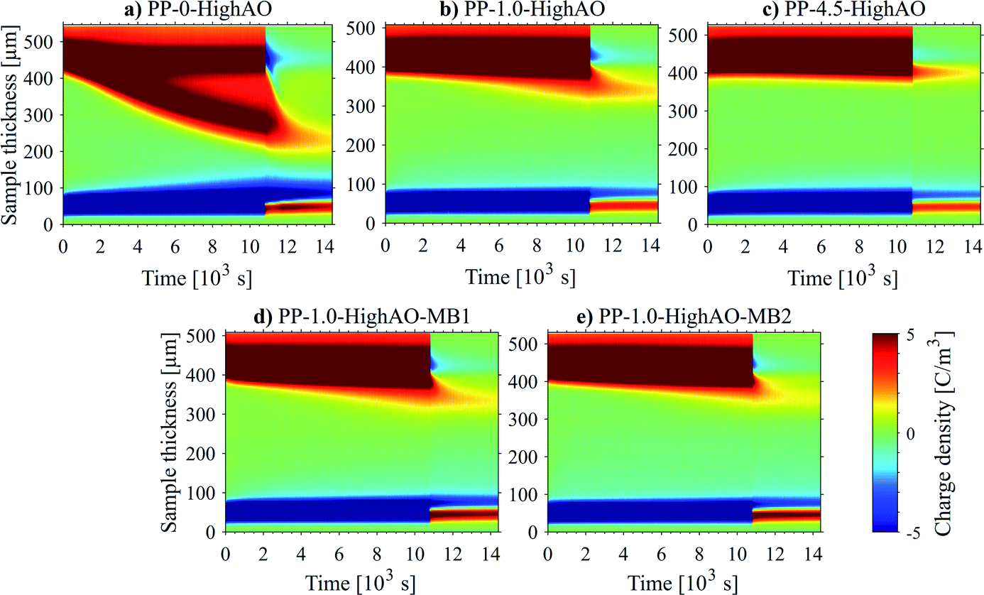 | ||
| Fig. 4 PEA space charge density vs. time profiles of selected PP–silica cast films (high AO) at 60 °C. Top row shows the compounds made via direct mixing: (a) unfilled reference, (b) 1.0 wt% silica–PP, (c) 4.5 wt% silica–PP. Bottom row shows 1.0 wt% compounds made via dilution of 4.5 wt% silica–PP masterbatch during (d) compounding and (e) cast film extrusion. Polarization field (50 V μm−1) was switched off at 10800 s. | ||
The situation was however greatly improved upon inclusion of nanosilica (Fig. 4c and d), with a general trend of reducing space charge with increasing silica content being evident (up to a nanofiller concentration limit which is generally near 5 wt%). Maximum local field enhancement is also strongly reduced, down to only 5%. Details on the amount of space charge stored in the bulk of the material, after the polarization period, and field enhancement is given in Table 1. The silica–PP nanocompounds also showed faster depolarization characteristics in comparison to neat PP; comparing the unfilled PP with the 4.5 wt% silica–PP, calculations on the charge depolarization trends indicated an increase in trap-controlled apparent mobility from ∼1.0 × 10⁻¹⁴ m2 V−1 s−1 to ∼1.3 × 10⁻¹² m2 V−1 s−1 (for details, see Table 1 and ref. 65). Such results are indicative of reduction of trap depth and density distribution upon incorporation of nanosilica,66 as confirmed by calculations reporting a decrease from 0.96 to 0.84 eV (see Table 1).
| Specimen | Stored charge [C m−3] | FEF | Apparent mobility [m2V−1s−1] | Trap depth [eV] |
|---|---|---|---|---|
| PP-0-HighAO | 3.12 | 1.40 | 0.75 × 10⁻¹⁴ | 0.96 |
| PP-1-HighAO | 1.41 | 1.21 | 0.37 × 10⁻¹³ | 0.92 |
| PP-4.5-HighAO | 0.46 | 1.05 | 0.69 × 10⁻¹² | 0.84 |
| PP-1-HighAO-MB1 | 1.25 | 1.14 | 0.39 × 10⁻¹³ | 0.93 |
| PP-1-HighAO-MB2 | 1.08 | 1.10 | 0.57 × 10⁻¹³ | 0.91 |
Characteristics of space charge accumulation were also investigated for specimens produced with the usage of a masterbatch route. Results in Fig. 4 show very mild differences in space charge accumulation and mobility of different samples, with a marginal improvement for specimens produced diluting a 4.5 wt% masterbatch during cast extrusion. All the tests reported an accumulation of charge under a poling field of 50 V μm−1, at 60 °C, from 1.41 to 1.08 C m−3, with a maximum local field enhancement from 20% to 10%. Trap depths and mobilities are estimated respectively around 0.9 eV, and in the range 0.37–0.57 × 10⁻¹³ m2V−1 s−1.
Biaxially oriented film properties
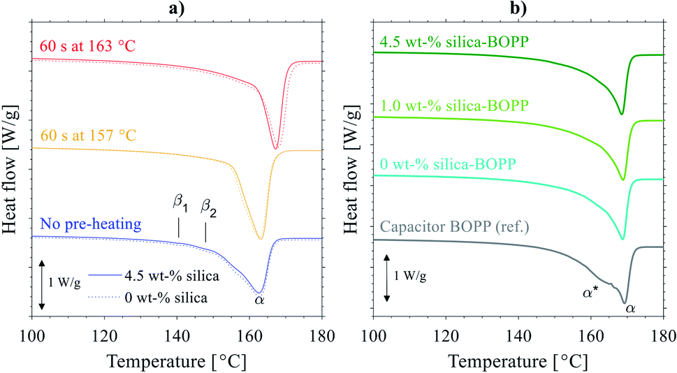 | ||
| Fig. 5 (a) DSC first heating scans of 4.5 wt% silica–PP (solid) and unfilled PP (dashed) cast films before and after pre-heating (relevant to biaxial stretching) for 60 s at 157–163 °C and cooling in room temperature. (b) DSC first heating scans of biaxially oriented 0–4.5 wt% silica–PP films along with a commercial capacitor BOPP film. | ||
Exemplifying DSC 1st heating endotherms of biaxially oriented thin films are presented in Fig. 5b along with a commercial capacitor BOPP reference: all the BOPP film melting endotherms corresponded to the monoclinic α-crystalline form PP with the peak melting temperatures in the range of 168–169 °C. For the commercial capacitor BOPP film, the main α-form melting peak also showed a low-temperature-side shoulder (α* peak) centered around 160–163 °C, being attributable to a second α-form crystallite population being present in the film. Interestingly, the α* peak was much less noticeable in the laboratory-scale films: this is due to the inherent differences between industrial tenter BOPP film production process68 and (simultaneous) laboratory-scale biaxial stretching,43 and it is assumed that the main α peak and the lower-temperature α* side peak are formed during (sequential) biaxial stretching and heat setting (annealing) of the film.69 Further, the fact that no β-form melting peak was detected in the 1st heating endotherms of BOPP films is associated with the β → α crystal transformation which had occurred during pre-heating and biaxial stretching of the film.3 Comparing the laboratory-scale BOPP films, a slight increase in degree of crystallinity was observed for the silica-BOPP nanocomposites, increasing from 55.7% (unfilled reference) to 57.6% (4.5 wt% silica-BOPP). Overall, the observed melting endotherms and the peak melting temperature range for the silica-BOPP films were similar to the industrially manufactured tenter-line BOPP film, with no significant morphological differences observed for the silica-BOPP nanocomposites.
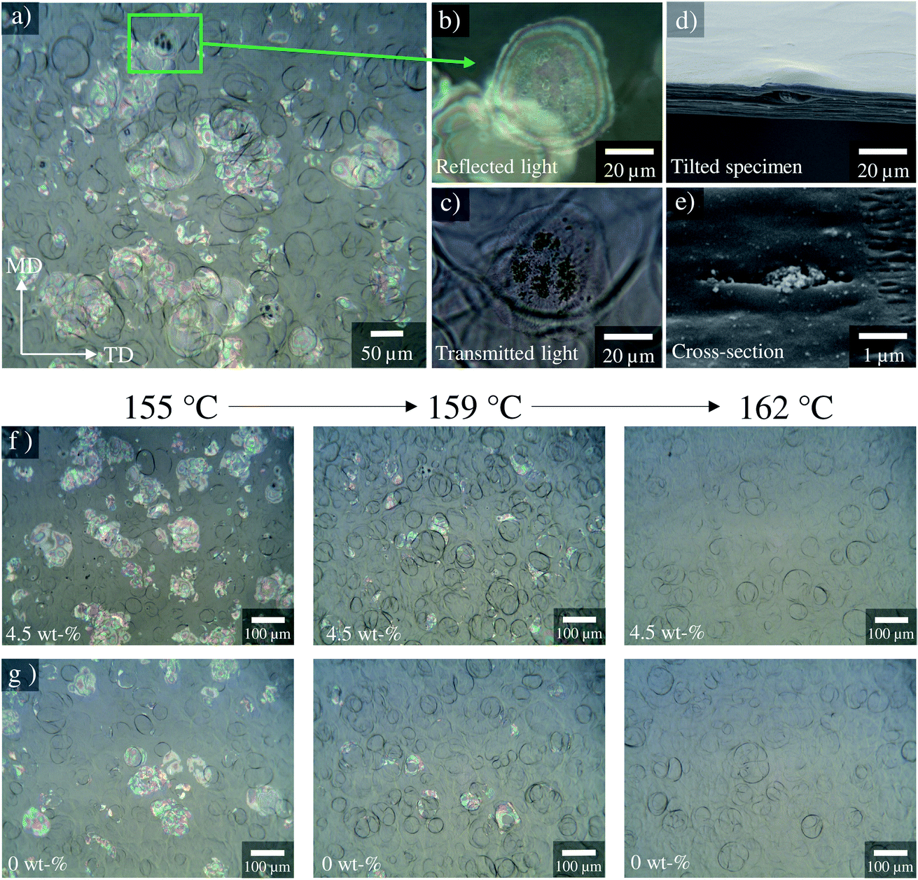 | ||
| Fig. 6 a) OM image of a 4.5 wt% silica-BOPP film (PP-4.5-HighAO, stretching temperature 157 °C, stretch ratio 6.0 × 6.0). A higher magnification of the circled (green) area is shown in (b) under reflected light and in (c) under transmitted light. The cross-sectional SEM images in (d) and (e) visualize the film cavitation caused by large agglomerates. Sequential OM images in (f) and (g) present the effect of increasing pre-heating and stretching temperature (155 → 159 → 162 °C) on the BOPP film morphology for 4.5 wt% silica-BOPP and reference BOPP film, respectively. MD: machine direction, TD: transverse direction. | ||
The influence of biaxial stretching temperature (from 155 °C to 163 °C) and stretch-ratio (up to 6.0 × 6.0) on the film morphology was studied in more detail. OM analysis of the morphological evolution of the studied silica-BOPP films under various biaxial stretching temperatures is presented in Fig. 6f and g for a 4.5 wt% silica composite and unfilled reference, respectively. Surface roughness characteristics measured from the both sides of the films using optical profilometry are presented in Fig. S2.† Finally, a comparison of machine directional (MD) stretch forces vs. stretch ratio at different temperatures is presented in Fig. S3† for a 4.5 wt% silica-BOPP composite.
At relatively low stretching temperatures (155 °C) voids were clearly observable using OM imaging (Fig. 6f and g) and the stretching forces (Fig. S3†) exhibited a typical ductile deformation behavior, showing a yield region around 1.3 stretch ratio followed by neck propagation and strain hardening, being consistent with Capt.67 As the stretching temperature was increased from 155 °C, the voids observable using OM were found to gradually decrease in size and quantity until at 162 °C (close to the melting point of isotactic PP), they were eliminated completely (Fig. 6f and g). With increasing stretching temperature the stretching forces decreased and began to show quasi rubber-like deformation characteristics72 with no observable yield point (Fig. S3†). Simultaneously, the BOPP film surface roughness (Fig. S2†) was found to exhibit an increasing trend with the stretching temperature. The formation of crater-like surface roughness upon biaxial stretching is closely related with the spherulitic morphology and collapse of trans-crystalline surface layer in the precursor cast film.43,73 The increase in surface roughness with the stretching temperature is in line with Tamura et al.,73 and can be related with the modification of the skin-layer morphology during pre-heating (see the POM cross-sectional images in Fig. S1†) and higher efficiency of the stretching-induced collapse of the crystal grain layer within the surface layers of the film. On the other hand, comparing the effect of nanosilica concentration on the surface roughness, similar or slightly lower surface roughness (between 159–163 °C) was observed on the chill roll (CR) side for the 1.0–4.5 wt% silica-BOPP films in comparison to the unfilled reference BOPP, while on the opposite side of chill roll (OCR) the differences in surface roughness values were statistically mostly insignificant.
The obtained results indicate that the biaxial stretching temperature is closely related with the presence or absence of voids inside the films. We note two mechanisms which may play a role here. Firstly, following the model proposed by Qaiss et al.,74 upon biaxial stretching the local stress concentration near the surface of the agglomerates/particles can result in decohesion at the particle–matrix interface, with this resulting in the initial pore formation and subsequent development into larger voids, see Fig. 7 for a schematic representation. The size of the particles/agglomerates and the stretching conditions obviously have a significant effect in the above process,75 as is also evidenced by the SEM-micrograph in Fig. 6e. When the biaxial stretching temperature is increased close to the melting point of the polymer, either the voided structure collapses,74 or the movement of the polymer chains and particles along the stretching direction becomes easier,75 hence eliminating the void formation. Indeed, the amount of molten polymer just above its melting point bearing high molecular mobility and nucleating power (“structured melt”) increases with the pre-heating/stretching temperature,67 hence reducing the stress concentration near particulates and giving rise to e.g. higher degree of crystallinity. On the other hand, a second relevant mechanism for the void formation is related to the presence of β-form crystallites in the precursor cast film: this has been previously associated with stretching-induced porosity/void formation in laboratory-scale BOPP films due to inter-(β-)lamellar cavitation and volume contraction effect due to the β → α crystal transformation.43 It is however interesting that the DSC analysis of the pre-heated cast films (Fig. 5a) indicated the absence of β-form crystallinity when biaxial stretching begins: this is understandable as the pre-heating was done above the melting point of β-crystallites (>147 °C). We also remark that the chill roll temperature in cast film extrusion was set so that the crystallization conditions for β-crystal formation were mostly unfavourable. Thus, the void formation for the films studied herein is presumably not dictated merely by the porosity formation related to β-crystallites,44 but it is rather caused by a combination of the above effects. However, even though the voids are eliminated by increasing the pre-heating and biaxial stretching temperature, the agglomerates/particles still remain in the film, having an impact on the dielectric properties.76
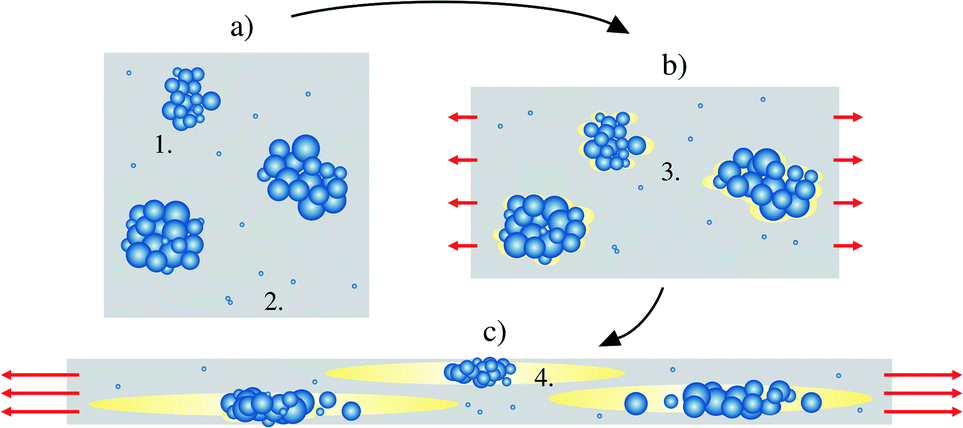 | ||
| Fig. 7 Schematic description of the agglomerate-induced cavitation and void-formation mechanism in biaxially stretched silica–PP films. (not in scale) The numbered regions are: 1. micron-sized silica agglomerate, 2. silica aggregate (in the nm-range), 3. initial stress-induced pore formation, 4. enlarged void formed upon biaxial stretching. | ||
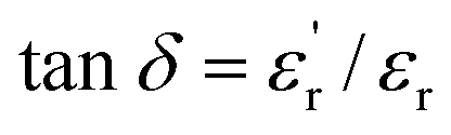 ) showed (i) a slight increase of tanδ below the glass transition temperature Tg (approx. −5 °C, see Table S1†), (ii) appearance of a new peak at ∼65 °C and (iii) reduction of dielectric loss at high temperatures. We attribute the slightly elevated tanδ at lower temperature and the emergence of a new relaxation peak for the silica–PP composites to the HMDS/silica–PP interface, bulk morphology and associated changes in the electronic structure. For the unfilled BOPP, the increase in tanδ at high temperature is likely related to the release of trapped charge and increase of DC conductivity (the effect was much pronounced at low frequencies), and this is likely an artifact related to charge injection during sample preparation (electrode evaporation). Such behavior was however mitigated for the silica-BOPP films, showing very low dielectric loss even at the highest temperatures. Fig. 8b presents the temperature- and frequency-dependent dielectric loss spectra of a 4.5 wt% silica-BOPP film, demonstrating that low dielectric loss level is maintained in the whole operation regime (note that the increase in tanδ at the highest frequencies in the MHz range is associated with the limitation of the thin film measurement cell rather than true film properties). Overall, the tanδ characteristics of the silica-BOPP films were found to be very promising, especially at the expected operating temperatures, as maintaining a low dielectric loss level is a prerequisite in high voltage metallized film capacitor applications.79
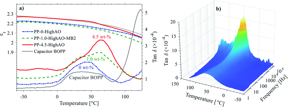 | ||
| Fig. 8 a) Relative permittivity (εr) and dielectric loss (tanδ) behavior of selected reference and silica-BOPP films as a function of temperature at 1 kHz (high antioxidant content, direct mixing). (b) Temperature- and frequency-dependent dielectric loss spectra of a 4.5 wt% silica-BOPP film (PP-4.5-HighAO, stretch-ratio 6.0 × 6.0). | ||
| W = kBTlog(vT) | (4) |
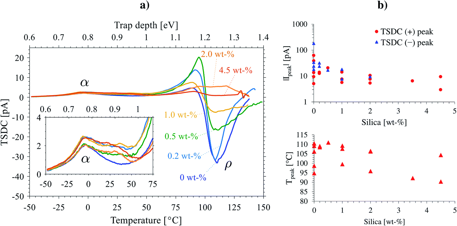 | ||
| Fig. 9 a) Thermally stimulated depolarization current (TSDC) spectra of selected 0–4.5 wt% silica-BOPP films. The inset shows a closer view of the lower temperature (shallow trap) region around glass transition temperature. Trap depth scale is presented for reference, calculated from eqn (4). (b) Bipolar TSDC peak current, |Ipeak|, in the deep trap region above 75 °C (top) and the deep trap peak temperature corresponding to the maximum (bipolar) TSDC peak amplitude (bottom) as a function of silica content. In top figure, the heteropolar (+) and homopolar (−) TSDC peak amplitudes are shown separately (absolute values on log-scale). | ||
For neat BOPP films, the typically observed TSDC features include:18,86 (i) a small heteropolar (α-) relaxation peak at −6 °C associable with de-trapping of charge from shallow traps as the polymer passes the glass-transition (cf. Table S1†) and (ii) a strong (bipolar) space charge (ρ-) relaxation in high temperature region (∼100 °C) which is due to the thermal release of captured charges from deep traps. The first TSDC peak was systematically observed around Tg for all the films (trap depth ∼0.75 eV). For the silica compounds however, the TSDC spectra above Tg became more pronounced and complex, indicating higher presence of shallow (or rather, “inter-level”87) traps with trap depths in the 0.7–0.9 eV range in comparison to neat BOPP. In the high temperature region (∼90 °C and above), the unfilled BOPP films exhibited strong TSDC peaks corresponding to charges released from deep traps (in the range of 1.1–1.3 eV), often being anomalous in the sense that the current flow was in the same direction as the polarization current (polarity reversal) which is a result from drifting of thermally de-trapped charge under the internal field caused by the space charge.86 For the silica-BOPP films however, the (bipolar) TSDC intensity in the deep trap region was greatly reduced, being indicative of modification of the apparent (occupied) deep trap density with nanosilica. This effect is demonstrated for several silica-BOPP films in Fig. 9b (top) where the peak current of the hetero- and homopolar TSDC peak amplitudes are plotted as a function of silica content, showing reduction in (bipolar) peak amplitude with increasing silica content. This can also be related with the reduced conductivity for the silica-BOPP nanocomposites (see below) resulting in less charge being accumulated in the traps during the poling phase prior to TSDC measurement. Further, the deep trap peak temperature is presented in Fig. 9b (bottom) as a function of silica content, showing that the deep trap peak location (comparable to trap depth) remains relatively unaffected by silica.
The fact that polymers exhibit complex TSDC spectra comprising of several overlapping of (quasi-) continuous trap bands—along with the TSDC polarity reversal effect observed in the deep trap region in Fig. 9a—complicate the analysis and evaluation of trapping parameters (trap depth and density of occupied states) as discussed in detail elsewhere.86,88 Due to these reasons we do not attempt e.g. peak-fitting,86 de-convolution89,90 or numerical methods91,92 to derive trap parameters here, as the results would be largely inconclusive.88 Nevertheless, the TSDC results presented herein clearly indicate a modification of trap density of states (DOS) and a more homogeneous distribution of charge in the silica-containing samples, and the results are consistent with the PEA space charge depolarization behavior measured from the non-oriented cast films (Fig. 4), thereby confirming the modification of charge trapping properties also in silica-BOPP thin films.
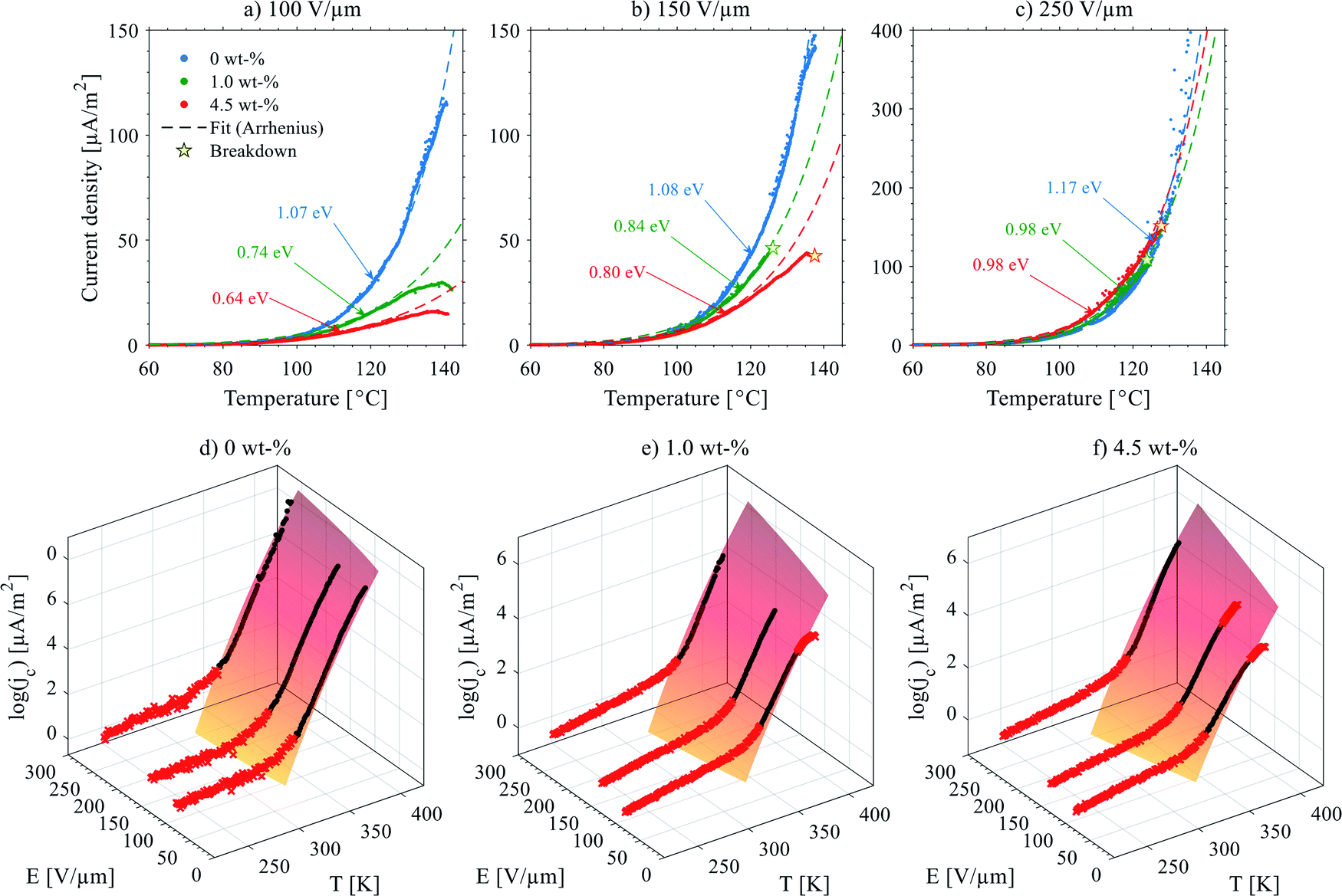 | ||
| Fig. 10 (top) Thermally stimulated polarization current (TSPC) spectra of selected 0–4.5 wt% silica-BOPP films (high antioxidant content) under (a) 100 V μm−1, (b) 150 V μm−1 and (c) 250 V μm−1 DC field. The dashed line is the fit to TSPC current density data according to eqn (5). Dielectric breakdown, if occurred during the TSPC measurement, is marked in the plot. (bottom) Temperature- and field-dependent conduction current density jc(T,E) derived from the high-field TSPC measurement of (d) 0 wt%, (e) 1.0 wt% and (f) 4.5 wt% silica-BOPP films (after subtraction of the temperature dependent polarization current density). The surface plot is the hopping -type conduction current model according to eqn (6) fitted to the main region (>300 K) where the main non-linear conduction current increase is observed. The red data points were excluded from the 3D fitting procedure. | ||
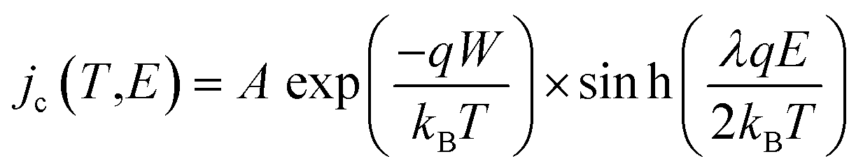
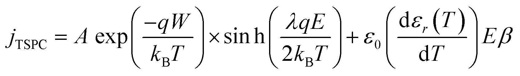
Due to the lack of polar groups in the polypropylene chain, the TSPC spectra of the silica-BOPP films are mainly associated with the high-field thermally stimulated transient conductivity. In comparison to fast voltage-ramp-based resistive (pre-breakdown) current measurement methods where, unless properly compensated for by sophisticated active cancellation,93 the capacitive current ic = C(dU/dt) can completely mask the (resistive) conduction current, one of the key benefits of the TSPC method is that only a minor capacitive current arises due to the relatively slow heating rate (dT/dt of 3 °C min−1) and weak temperature dependence of the sample capacitance C(T). The TSPC current density jTSPC is given by:80
 | (5) |
 | (6) |
 | (7) |
 | (8) |
The conduction current density models fitted to the TSPC data in accordance to eqn (8) at a given field strength are presented in Fig. 10 (dashed lines) along with the associated trap depths (see also Table 2). Firstly, the calculated Arrhenius activation energies (i.e. trap depth) increased with increasing field stress, being consistent with the observations of Li et al. for a tenter BOPP film in ref. 93. Secondly, incorporation of nanosilica is found to provide a significant reduction in effective trap depth (from ∼1.07 eV of unfilled BOPP down to 0.64 eV for 4.5 wt% silica-BOPP nanocomposite at 100 V μm−1), being consistent with the results derived from the PEA space charge measurement of non-stretched cast films and the TSDC results of the biaxially stretched films. Previously, Kahouli et al. have measured a deep trap level of 1.05 eV for neat BOPP and associated with ionic conduction at high temperature due to traps present in the crystalline phase;5 in this view, the reduced effective trap depth of 4.5 wt% silica-BOPP nanocomposite can be related to morphological changes (disorder) in polymer matrix due to nanosilica. The temperature- and field-dependent conductivity characteristics were investigated further by performing 3D fitting of eqn (8) into the TSPC spectra, see Fig. 10d. The extracted trap parameters (trap depth and mean hopping distance) are given in Table 2. The (mean) trap depths derived from the 3D fitting procedure were found to fall within the range of activation energies derived at fixed field stresses, ranging from 1.10 eV (unfilled BOPP) to ∼0.9 eV (silica-BOPP), hence confirming the reduction of apparent trap depth with nanosilica. The hopping distance λ was found to increase from 0.21 nm (unfilled BOPP) to 0.72 nm (4.5 wt% silica): while hopping distance values in the similar range have also been reported previously for e.g. BOPP, PET and PS films,16,95 the values for λ derived herein are generally very low when relating them to resulting trap density (in the range of 1027 m−3 or more)5,15 and certainly too low to be linked with the silica inter-particle distance statistics (see Fig. 3d). Aside from the evident limitation of the hopping conduction model to fully describe the TSPC process, the most intriguing feature for the TSPC spectra of the silica-BOPP films in Fig. 10 is however the saturation (or even decrease) of the thermally stimulated conduction current at the highest temperatures of >120 °C under moderate electric field stresses (<250 V μm−1), an effect which becomes more pronounced with increasing silica concentration from 1.0 to 4.5 wt%. Such anomalous behavior of conductivity cannot be explained by the present conduction model. Thorough understanding of such dynamic conduction phenomena in silica-BOPP nanocomposite would necessitate more thorough investigation by e.g. fluid models of charge transport, something which is not to be covered in this study.
| Code | Arrhenius-fit (fixed field) | Trap parameters (3D fit) | |||||
|---|---|---|---|---|---|---|---|
| E [V μm−1] | W [eV] | W [eV] | λ [nm] | ||||
| PP-0-HighAO | 100 | 1.07 | (1.05–1.08) | 1.10 | (1.09–1.12) | 0.21 | (0.15–0.28) |
| 150 | 1.08 | (1.07–1.09) | |||||
| 250 | 1.17 | (1.15–1.20) | |||||
| PP-1.0-HighAO | 100 | 0.74 | (0.72–0.76) | 0.92 | (0.90–0.94) | 0.47 | (0.44–0.49) |
| 150 | 0.84 | (0.83–0.85) | |||||
| 250 | 0.98 | (0.96–1.00) | |||||
| PP-4.5-HighAO | 100 | 0.64 | (0.63–0.65) | 0.91 | (0.88–0.94) | 0.72 | (0.69–0.76) |
| 150 | 0.80 | (0.79–0.81) | |||||
| 250 | 0.98 | (0.97–1.00) | |||||
 | (9) |
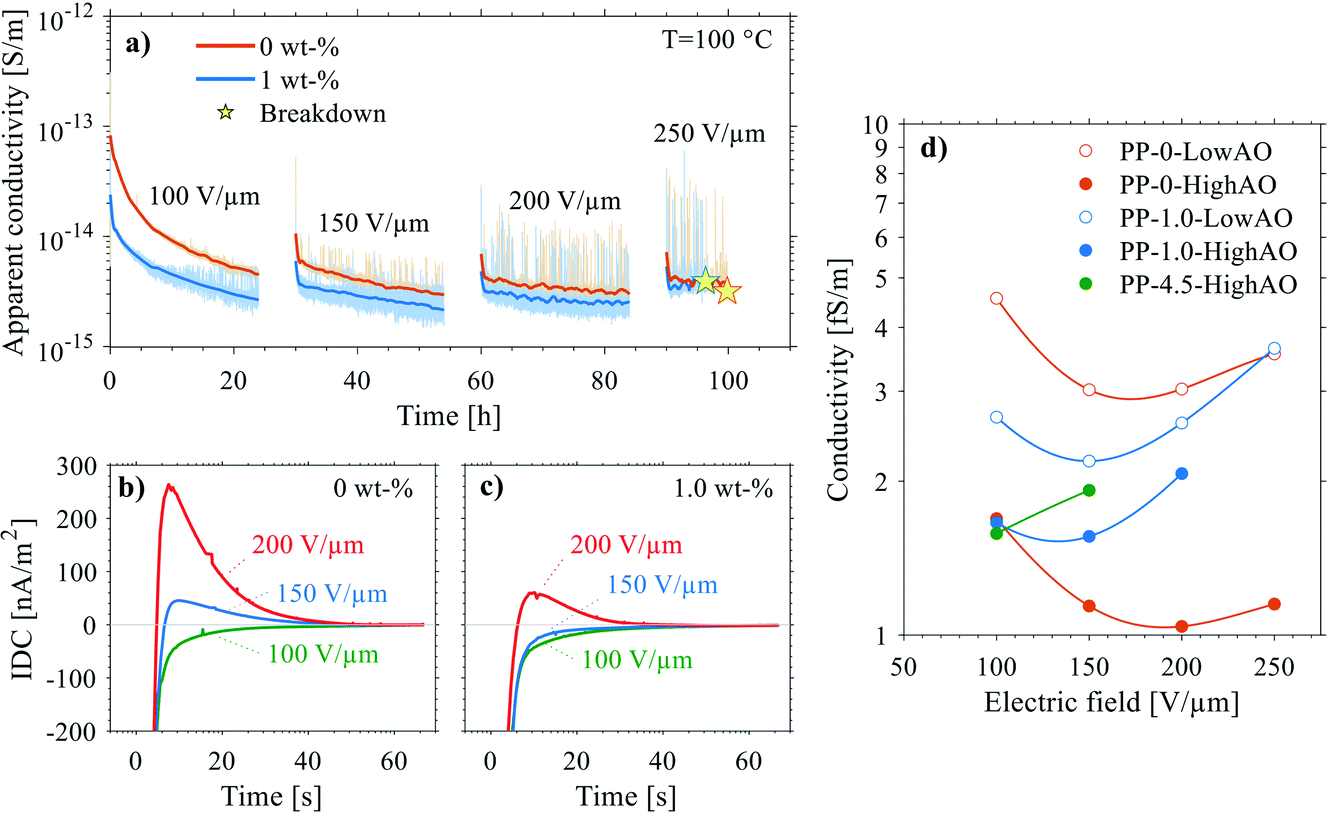 | ||
| Fig. 11 a) Apparent conductivity (cf. charging current density) of 0 wt% and 1.0 wt% silica-BOPP films (low antioxidant content) as a function of time under step-wise increasing DC electric field (100–250 V μm−1) at 100 °C. The polarization time for each field stress condition was 24 h, followed by 6 h of depolarization before application of the next field stress. The light colored traces are the raw data and the superimposed solid lines are the Savitzky–Golay filtered data to better show the underlying conductivity trend. (b) and (c) show the isothermal depolarization current density as a function of time for 0 wt% and 1.0 wt% silica-BOPP specimens after polarization at 100–250 V μm−1, respectively. (d) Conductivity at the end of 24 h polarization as a function of step-wise electric field stress at 100 °C for selected 0–4.5 wt% silica-BOPP specimens. The solid lines are cubic splines to guide eyes. | ||
On the other hand, the isothermal depolarization current (IDC) trends recoded in-between the polarization steps, see Fig. 11b and c, exemplify the dependence of depolarization current density on the preceding polarization field stress for unfilled reference BOPP and 1.0 wt% silica-BOPP. After the initial polarization step for 24 h under 100 V μm−1 at 100 °C, both the samples showed normal IDC trends (i.e. with IDC having opposite polarity in comparison to the polarization current), with however slightly slower decay rate observable for the 1.0 wt% silica BOPP. Again, this can be attributed to the modified (apparent) density and depth of deep trapping sites for silica-nanocompounds. Interestingly, with subsequently increasing polarization field and (total) measurement time, an anomalous current component (i.e. a current component with the same polarity as the polarization current) became observable during the first 100 s of depolarization, with this effect being stronger in the unfilled reference BOPP. Recently, Hoang et al. have elucidated the occurrence of anomalous discharge currents (ADC) in unfilled and nano-filled LDPE samples in similar time scales by employing a bipolar charge injection model.84 The existence of the reverse depolarization current component is associated with the temperature-assisted drift of charge carriers in the regions of positive and negative (internal) field formed by the accumulated space charge within the sample. Thus, the ADC behavior is similar to the polarity reversal observed under thermally stimulated conditions (TSDC), being related to the zero-field phenomenon caused by space charge.86 In principle, the initial high density of injected charge near the electrodes causes a strong negative field and gives a rise to the negative discharge current. However, after the rapid depletion of injected charge near the electrodes, the positive discharge current component, associated with the drifting of charge trapped spatially deeper in the dielectric, becomes dominant. This imbalance between the decay rates and magnitudes of the positive and negative discharge current components gives a rise to the ADC, and it is directly linked to the trap density of states and depolarization temperature. Therefore, the mitigated ADC effect observable for the silica-BOPP film in Fig. 11c can be related to a beneficial modification of deep trap states, similarly as observed by Hoang et al. for LDPE/Al2O3 nanocomposites.84
 | (10) |
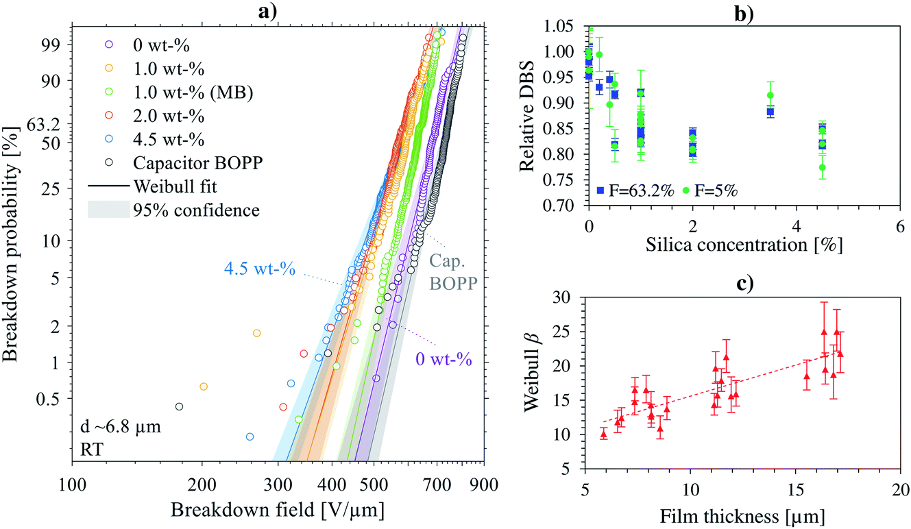 | ||
| Fig. 12 a) Exemplifying room temperature DC large-area multi-breakdown distributions of selected 0–4.5 wt% silica-BOPP films (high antioxidant content) on Weibull scale. Biaxial stretching ratio was 6.0 × 6.0 and stretching temperature was 161 °C. The solid lines and the shaded areas are the 2-parameter Weibull fits and the 95% confidence bounds, respectively. The mean film thickness is ∼6.8 μm. (b) Relative dielectric breakdown strength (DBS) at 5% and 63.2% breakdown probabilities (relative to unfilled reference) for various 0–4.5 wt% silica-BOPP films with varying film thickness and processing. (c) Dependence of 2-p Weibull β parameter on mean BOPP film thickness. The error bars in (b) and (c) denote 90% confidence. | ||
Several laboratory-scale compounding and film production trials were performed during which aspects related to mixing and de-agglomeration efficiency, cast film extrusion and biaxial stretching parameters were studied: these data are summarized for relative change of large-area DBS in Fig. 12b, and for thickness-dependence of the Weibull β parameter in Fig. 12c. It is evident from Fig. 12b that, in comparison to unfilled reference BOPP, a similar decreasing trend in large-area dielectric breakdown strength with increasing silica concentration was prominent for all the silica-BOPP variants in 5–17 μm thickness range. Moreover, a clear decrease of the Weibull β parameter with decreasing BOPP film thickness is evident from Fig. 12c, highlighting the increasingly detrimental role of agglomerates and the challenge of producing defect-free nanocomposite thin films when the material is pushed (or stretched) to its limits.39 Analogous to the weakest-link-type failure mechanism, the increased local breakdown propensity due to the non-ideal silica dispersion and the presence of micron-sized agglomerates can mask the otherwise beneficial bulk-type properties brought by the nanosilica (such as modified trap DOS, reduced conductivity and mitigated space charge) both in short-term progressive-stress dielectric breakdown tests (reaching extreme field conditions)33 as well as in medium-to long-term voltage endurance and ageing tests under accelerated electrical and thermal stresses.14,99,100 Preliminary electro-thermal ageing test results from similar silica-BOPP nanocomposite films produced in industrial scale are presented in another study.99
Conclusions
Pilot-scale capacitor PP nanocomposite films incorporating hydrophobic fumed silica nanoparticles were prepared via an industrially relevant melt-blending, film extrusion and biaxial stretching approach, and comprehensive investigation of processing–structure–property relationships was carried out to provide a critical evaluation of the performance potential and current technological limitations of state-of-the-art silica-BOPP nanocomposite films aimed for HVDC film capacitor applications. Incorporation of fumed nanosilica can bring about promising bulk dielectric property modifications under moderate electro-thermal stresses (up to ∼200 V μm−1 at 100 °C) including decreased high field/high temperature conductivity, modification of the trap density of states, low dielectric losses and reduced space charge accumulation, all being beneficial property enhancements for metallized film capacitor applications. However, further improvement of nanoparticle dispersion and film morphology are still seen necessary as film structural defects (voids) and localized electrical weak points caused by silica agglomerates can deteriorate the nanocomposite film performance under high electro-thermal stress. Achieving homogeneous morphology in biaxially oriented thin films is perhaps one of the most challenging tasks in the field of dielectric nanocomposites at the moment limiting, as issues such as nanoparticle agglomeration and structural inhomogeneities (e.g. cavities) become increasingly critical as the film thickness is decreased and the material is pushed to its limits, hence limiting industrial scale application.Author contributions
I. R. conceived the overall design, characterization, analysis and manuscript writing with support and comments from the other authors. I. R., E. S., T. F. and M. P. performed the material compounding and sample manufacturing at VTT. I. R. conducted the morphological characterization and analysis. P. S. and H. N. performed the PEA characterization for cast films at University of Bologna. I. R., M. N. and K. L. performed the thin film dielectric characterization at Tampere University. I. R. performed formal data analysis. M. P. was responsible for the project funding acquisition and supervision.Conflicts of interest
There are no conflicts to declare.Acknowledgements
This project has received funding from the European Union's Horizon 2020 research and innovation programme under grant agreement No 720858.References
- Y. Tang, L. Ran, O. Alatise and P. Mawby, IEEE Trans. Ind. Appl., 2016, 52, 3279–3293 CAS.
- M. Ritamäki, I. Rytöluoto and K. Lahti, IEEE Trans. Dielectr. Electr. Insul., 2019, 26, 1229–1237 Search PubMed.
- I. Rytöluoto, A. Gitsas, S. Pasanen and K. Lahti, Eur. Polym. J., 2017, 95, 606–624 CrossRef.
- M. DeMeuse, Biaxial Stretching of Film, Woodhead Publishing Limited, Cambridge, 1st edn, 2011 Search PubMed.
- A. Kahouli, O. Gallot-Lavallée, P. Rain, O. Lesaint, C. Guillermin and J.-M. Lupin, J. Appl. Polym. Sci., 2015, 132, 42224 Search PubMed.
- European Plastics Innovation Awards, 2016 Search PubMed.
- X. Qi, Z. Zheng and S. Boggs, IEEE Electr. Insul. Mag., 2004, 20, 27–34 Search PubMed.
- S. J. Laihonen, U. Gäfvert, T. Schütte and U. W. Gedde, IEEE Trans. Dielectr. Electr. Insul., 2007, 14, 275–286 CAS.
- V. O. Belko, O. A. Emelyanov, I. O. Ivanov and A. P. Plotnikov, IEEE Trans. Plasma Sci., 2021, 49, 1580–1587 CAS.
- H. Li, Y. Zhou, Y. Liu, L. Li, Y. Liu and Q. Wang, Chem. Soc. Rev., 2021, 50, 6369–6400 RSC.
- M. A. Schneider, J. R. Macdonald, M. C. Schalnat and J. B. Ennis, in Proceedings of the 2012 IEEE International Power Modulator and High Voltage Conference, IPMHVC 2012, 2012, pp. 284–287 Search PubMed.
- J. S. Ho and S. G. Greenbaum, ACS Appl. Mater. Interfaces, 2018, 10, 29189–29218 CrossRef CAS PubMed.
- F. Zheng, Y. Miao, J. Dong, Z. An, Q. Lei and Y. Zhang, IEEE Trans. Dielectr. Electr. Insul., 2016, 23, 3102–3107 CAS.
- M. Ritamäki, I. Rytöluoto, K. Lahti, T. Vestberg, S. Pasanen and T. Flyktman, IEEE Trans. Dielectr. Electr. Insul., 2017, 24, 826–836 Search PubMed.
- J. Ho and T. R. Jow, IEEE Trans. Dielectr. Electr. Insul., 2012, 19, 990–995 CAS.
- Z. Li, H. Uehara, R. Ramprasad, S. Boggs and Y. Cao, in 2015 IEEE Conference on Electrical Insulation and Dielectric Phenomena (CEIDP), IEEE, 2015, pp. 872–875 Search PubMed.
- H. Li, L. Li, L. Li, W. Wang, X. Huang, Q. Chen and F. Lin, IEEE Trans. Dielectr. Electr. Insul., 2017, 24, 1870–1877 Search PubMed.
- M. Ritamäki, I. Rytöluoto and K. Lahti, IEEE Trans. Dielectr. Electr. Insul., 2019, 26, 1229–1237 Search PubMed.
- M. Ritamäki, I. Rytöluoto and K. Lahti, in 2018 IEEE International Conference on Dielectrics (ICD), 2018 Search PubMed.
- Z. Wang, Y. Zhang, H. Wang and F. Blaabjerg, IEEE Trans. Power Electron., 2020, 35, 5589–5593 Search PubMed.
- L. Chen, R. Ramprasad, R. Batra, R. Ranganathan, G. Sotzing and Y. Cao, Chem. Mater., 2018, 30, 7699–7706 CrossRef CAS.
- H.-V. Nguyen and T. H. Pham, Phys. Status Solidi, 2017, 1700036 Search PubMed.
- S. K. Kumar, B. C. Benicewicz, R. A. Vaia and K. I. Winey, Macromolecules, 2017, 50, 714–731 CrossRef CAS.
- H. Luo, X. Zhou, C. Ellingford, Y. Zhang, S. Chen, K. Zhou, D. Zhang, C. R. Bowen and C. Wan, Chem. Soc. Rev., 2019, 48, 4424–4465 RSC.
- X. He, I. Rytoluoto, R. Anyszka, A. Mahtabani, E. Saarimaki, K. Lahti, M. Paajanen, W. Dierkes and A. Blume, IEEE Access, 2020, 8, 87719–87734 Search PubMed.
- A. Mahtabani, I. Rytöluoto, R. Anyszka, X. He, E. Saarimäki, K. Lahti, M. Paajanen, W. Dierkes and A. Blume, ACS Appl. Polym. Mater., 2020, 2, 3148–3160 CrossRef CAS.
- D. Tan, L. Zhang, Q. Chen and P. Irwin, J. Electron. Mater., 2014, 43, 4569–4575 CrossRef CAS.
- L. An, S. A. Boggs and J. P. Calame, Proc. 2008 IEEE Int. Power Modul. High Volt. Conf. PMHVC, 2008, vol. 24, pp. 552–555 Search PubMed.
- G. Zhang, D. Brannum, D. Dong, L. Tang, E. Allahyarov, S. Tang, K. Kodweis, J.-K. Lee and L. Zhu, Chem. Mater., 2016, 28, 4646–4660 CrossRef CAS.
- B. Liu, M. Yang, W. Y. Zhou, H. W. Cai, S. L. Zhong, M. S. Zheng and Z. M. Dang, Energy Storage Mater., 2020, 27, 443–452 CrossRef.
- W. Liu, L. Cheng and S. Li, Compos. Commun., 2018, 10, 221–225 CrossRef.
- M. Streibl, R. Karmazin and R. Moos, IEEE Trans. Dielectr. Electr. Insul., 2018, 25, 2429–2442 CAS.
- I. Rytöluoto, K. Lahti, M. Karttunen, M. Koponen, S. Virtanen and M. Pettersson, IEEE Trans. Dielectr. Electr. Insul., 2015, 22, 2196–2206 Search PubMed.
- I. Rytöluoto, M. Ritamäki, K. Lahti, M. Paajanen, M. Karttunen, G. C. Montanari, P. Seri and H. Naderiallaf, in 2018 IEEE 2nd International Conference on Dielectrics (ICD), IEEE, Budapest, Hungary, 2018, pp. 1–4 Search PubMed.
- G. C. Montanari, P. Seri, M. Paajanen, K. Lahti, I. Rytöluoto, M. Ritamäki, A. Blume, W. Dierkes, A. Mahtabani and X. He, in IEEE International Conference on Dielectrics (ICD), IEEE, Budapest, 2018 Search PubMed.
- I. Rytöluoto, M. Niittymäki, K. Lahti, E. Saarimäki, T. Flyktman, M. Paajanen and M. Karttunen, Proc. Nord. Insul. Symp., 2019, pp. 123–128 Search PubMed.
- M. Streibl, S. Werner, J. Kaschta, D. W. Schubert and R. Moos, IEEE Trans. Dielectr. Electr. Insul., 2020, 27, 468–475 CAS.
- M. Takala, H. Ranta, P. Nevalainen, P. Pakonen, J. Pelto, M. Karttunen, S. Virtanen, V. Koivu, M. Pettersson, B. Sonerud and K. Kannus, IEEE Trans. Dielectr. Electr. Insul., 2010, 17, 1259–1267 CAS.
- D. Q. Tan, Adv. Funct. Mater., 2019, 1808567, 1–23 Search PubMed.
- S. Werner, J. Kaschta and D. W. Schubert, in ETG-Symposium VDE High Voltage Technology, 2020, pp. 1–8 Search PubMed.
- F. J. Lanyi, N. Wenzke, J. Kaschta and D. W. Schubert, Adv. Eng. Mater., 2020, 22, 1900796 CrossRef CAS.
- I. Rytöluoto, K. Lahti, M. Karttunen and M. Koponen, IEEE Trans. Dielectr. Electr. Insul., 2015, 22, 689–700 Search PubMed.
- I. Rytöluoto, A. Gitsas, S. Pasanen and K. Lahti, Eur. Polym. J., 2017, 95, 606–624 CrossRef.
- G. T. Offord, S. R. Armstrong, B. D. Freeman, E. Baer, A. Hiltner, J. S. Swinnea and D. R. Paul, Polymer, 2013, 54, 2577–2589 CrossRef CAS.
- G. T. Offord, S. R. Armstrong, B. D. Freeman, E. Baer, A. Hiltner and D. R. Paul, Polymer, 2013, 54, 2796–2807 CrossRef CAS.
- Y. Yamamoto, Y. Inoue, T. Onai, C. Doshu, H. Takahashi and H. Uehara, Macromolecules, 2007, 40, 2745–2750 CrossRef CAS.
- P. Jacoby, Beta Nucleation of Polypropylene – Properties, Technology, and Applications, William Andrew, PDL handbook series, 1st edn, 2013 Search PubMed.
- K. H. Nitta, K. Asuka, B. Liu and M. Terano, Polymer, 2006, 47, 6457–6463 CrossRef CAS.
- D. N. Bikiaris, G. Z. Papageorgiou, E. Pavlidou, N. Vouroutzis, P. Palatzoglou and G. P. Karayannidis, J. Appl. Polym. Sci., 2006, 100, 2684–2696 CrossRef CAS.
- S. H. Kim, S. H. Ahn and T. Hirai, Polymer, 2003, 44, 5625–5634 CrossRef CAS.
- S. J. Laihonen and H. Greijer, Proc. Nord. Insul. Symp., 2019, pp. 37–42 Search PubMed.
- M. Xiao, B. Du, R. Xu, Z. Ran, H. Liu, J. Xing and K. Fan, in Polymer Insulation Applied for HVDC Transmission, Springer Singapore, Singapore, 2021, pp. 627–651 Search PubMed.
- R. R. Xu, B. X. Du, M. Xiao, J. Li, H. L. Liu, Z. Y. Ran and J. W. Xing, Polymer, 2021, 213, 123204 CrossRef CAS.
- Z. Y. Ran, B. X. Du, M. Xiao, H. L. Liu and J. W. Xing, IEEE Trans. Dielectr. Electr. Insul., 2021, 28, 175–182 CAS.
- J. L. Nash, Polym. Eng. Sci., 1988, 28, 862–870 CrossRef CAS.
- G. Z. Papageorgiou, D. S. Achilias, D. N. Bikiaris and G. P. Karayannidis, Thermochim. Acta, 2005, 427, 117–128 CrossRef CAS.
- X. Cao, M. Wu, A. Zhou, Y. Wang, X. He and L. Wang, e-Polym., 2017, 17, 373–381 CAS.
- X. Liu and Q. Wu, Eur. Polym. J., 2002, 38, 1383–1389 CrossRef CAS.
- S. Jain, H. Goossens, M. Van Duin and P. Lemstra, Polymer, 2005, 46, 8805–8818 CrossRef CAS.
- S. Zhou, W. Wang, Z. Xin, S. Zhao and Y. Shi, J. Mater. Sci., 2016, 51, 5598–5608 CrossRef CAS.
- Evonik Industries – AEROSIL® – Fumed Silica: Technical Overview, 2015, pp. 1–104 Search PubMed.
- A. M. Pourrahimi, R. T. Olsson and M. S. Hedenqvist, Adv. Mater., 2017, 1703624, 1703624 Search PubMed.
- P. P. Bansal and A. J. Ardell, Metallography, 1972, 5, 97–111 CrossRef.
- L. Simoni, IEEE Trans. Electr. Insul., 1982, EI-17, 375 Search PubMed.
- G. Mazzanti, G. C. Montanari and J. M. Alison, IEEE Trans. Dielectr. Electr. Insul., 2003, 10, 187–197 CrossRef.
- G. C. Montanari, P. Seri, M. Ritamäki, K. Lahti, I. Rytöluoto and M. Paajanen, Proc. IEEE Int. Conf. Prop. Appl. Dielectr. Mater., 2018, pp. 41–44 Search PubMed.
- L. Capt, Simultaneous biaxial stretching of isotactic polypropylene films in the partly molten state, PhD thesis, McGill University, 2003.
- J. Breil, in Film Processing Advances, ed. T. Kanai and G. A. Campbell, Hanser, Münich, 2014, pp. 193–229 Search PubMed.
- M. B. Elias, R. Machado and S. V. Canevarolo, J. Therm. Anal. Calorim., 2000, 59, 143–155 CrossRef CAS.
- S. Tamura and T. Kanai, J. Appl. Polym. Sci., 2013, 130, 3555–3564 CrossRef CAS.
- S. Sängerlaub, M. Böhmer and C. Stramm, J. Appl. Polym. Sci., 2013, 129, 1238–1248 CrossRef.
- D. Gloger, E. Rossegger, M. Gahleitner and C. Wagner, J. Polym. Eng., 2019, 1–10 Search PubMed.
- S. Tamura, K. Ohta and T. Kanai, J. Appl. Polym. Sci., 2012, 124, 2725–2735 CrossRef CAS.
- A. Qaiss, H. Saidi, O. Fassi-Fehri and M. Bousmina, J. Appl. Polym. Sci., 2012, 123, 3425–3436 CrossRef CAS.
- X. Zhang, Q. Xing, R. Li, R. Wang and D. Wang, Chin. J. Polym. Sci., 2013, 31, 275–284 CrossRef CAS.
- X. Qiu, F. Groth, W. Wirges and R. Gerhard, IEEE Trans. Dielectr. Electr. Insul., 2018, 25, 829–834 CAS.
- I. Rytöluoto, M. Ritamäki and K. Lahti, in 2018 12th International Conference on the Properties and Applications of Dielectric Materials (ICPADM), IEEE, 2018, pp. 289–292 Search PubMed.
- I. Rytöluoto, M. Ritamäki, A. Gitsas, S. Pasanen and K. Lahti, in Proceedings of the Nordic Insulation Symposium, 2017, DOI:10.5324/nordis.v0i25.2359.
- T. D. Huan, S. Boggs, G. Teyssedre, C. Laurent, M. Cakmak, S. Kumar and R. Ramprasad, Prog. Mater. Sci., 2016, 83, 236–269 CrossRef CAS.
- Electrets, ed., G. M. Sessler, Springer Berlin Heidelberg, Berlin, Heidelberg, 1987, vol. 33 Search PubMed.
- J. Belana, J. A. Diego, J. Orrit, I. Tamayo and M. Mudarra, IEEE Trans. Dielectr. Electr. Insul., 2011, 18, 2074–2082 CAS.
- S. Le Roy, F. Baudoin, L. Boudou, C. Laurent and G. Teyssèdre, in Proceedings of the 2010 IEEE International Conference on Solid Dielectrics, ICSD 2010, 2010, pp. 4–7 Search PubMed.
- F. Namouchi, W. Jilani and H. Guermazi, J. Non-Cryst. Solids, 2015, 427, 76–82 CrossRef CAS.
- A. T. Hoang, Y. V. Serdyuk and S. M. Gubanski, Energies, 2020, 13, 1518 CrossRef CAS.
- M. Meunier and N. Quirke, J. Chem. Phys., 2000, 113, 369–376 CrossRef CAS.
- I. Rytöluoto, M. Niittymäki and K. Lahti, Proc. Nord. Insul. Symp., 2019, pp. 64–69 Search PubMed.
- E. Doedens, E. M. Jarvid, R. Guffond and Y. V. Serdyuk, Energies, 2020, 13, 1750 CrossRef.
- G. Teyssedre, F. Zheng, L. Boudou and C. Laurent, J. Phys. D: Appl. Phys., 2021, 12 Search PubMed.
- M. Aldana, E. Laredo, A. Bello and N. Suarez, J. Polym. Sci., Part B: Polym. Phys., 1994, 32, 2197–2206 CrossRef CAS.
- Y. Wang, J. Wu and Y. Yin, IEEE Trans. Dielectr. Electr. Insul., 2017, 24, 3138–3143 CAS.
- F. Tian, W. Bu, L. Shi, C. Yang, Y. Wang and Q. Lei, J. Electrost., 2011, 69, 7–10 CrossRef.
- J. G. Simmons, G. W. Taylor and M. C. Tam, Phys. Rev. B: Solid State, 1973, 7, 3714–3719 CrossRef CAS.
- Z. Li, C. Xu, H. Uehara, S. Boggs and Y. Cao, AIP Adv., 2016, 6, 115025 CrossRef.
- E. Logakis, L. Herrmann and T. Christen, IEEE Trans. Dielectr. Electr. Insul., 2016, 23, 142–148 CAS.
- H. Li, Z. Li, F. Lin, D. Liu, B. Wang, Y. Chen, L. Dai and S. Fan, J. Electrost., 2013, 71, 958–962 CrossRef CAS.
- H. Ghorbani, T. Christen, M. Carlen, E. Logakis, L. Herrmann, H. Hillborg, L. Petersson and J. Viertel, IEEE Trans. Dielectr. Electr. Insul., 2017, 24, 1485–1493 CAS.
- C. Xu, J. Ho and S. A. Boggs, IEEE Electr. Insul. Mag., 2008, 24, 30–34 Search PubMed.
- S. J. Laihonen, A. Gustafsson, U. Gäfvert, T. Schütte and U. W. Gedde, IEEE Trans. Dielectr. Electr. Insul., 2007, 14, 263–274 CAS.
- K. Lahti, I. Rytöluoto, M. Niittymäki, E. Saarimäki and M. Paajanen, in IEEE International Conference on Dielectrics, 2020, pp. 661–664 Search PubMed.
- I. Rytöluoto, M. Ritamäki, K. Lahti and M. Karttunen, in 2015 IEEE 11th International Conference on the Properties and Applications of Dielectric Materials (ICPADM), 2015 Search PubMed.
Footnote |
| † Electronic supplementary information (ESI) available. See DOI: 10.1039/d1ta10336a |
| This journal is © The Royal Society of Chemistry 2022 |