
 Open Access Article
 This Open Access Article is licensed under a Creative Commons Attribution-Non Commercial 3.0 Unported Licence
Role of pO2 and film microstructure on the memristive properties of La2NiO4+δ/LaNiO3−δ bilayers†
Klaasjan
Maas
a,
Chloé
Wulles
ab,
Jose Manuel
Caicedo Roque
b,
Belén
Ballesteros
 b,
Valentin
Lafarge
ab,
José
Santiso
*b and
Mónica
Burriel
*a
b,
Valentin
Lafarge
ab,
José
Santiso
*b and
Mónica
Burriel
*a
aUniv. Grenoble Alpes, CNRS, Grenoble INP, LMGP, 38000 Grenoble, France. E-mail: monica.burriel@grenoble-inp.fr
bCatalan Institute of Nanoscience and Nanotechnology (ICN2), CSIC and the Barcelona Institute of Science and Technology (BIST), Campus UAB, 08193 Bellaterra, Barcelona, Spain. E-mail: jose.santiso@icn2.cat
First published on 2nd February 2022
Abstract
LaNiO3/La2NiO4 bilayers deposited at varying pO2 conditions resulted in remarkable differences in film microstructure and cell parameters, directly affecting the electrical behaviour of Pt/LaNiO3/La2NiO4/Pt devices. The devices deposited at low pO2 showed the largest memristance. We propose this is due to the formation of a p-type Schottky contact between LaNiO3 and La2NiO4, where the extent of its carrier depletion width can be modulated by the electric-field induced drift of interstitial oxygen ions acting as mobile acceptor dopants in La2NiO4.
Introduction
Mixed ionic electronic conducting materials (MIEC) based on transition metal oxides are key elements in many different applications, such as ceramic gas separation membranes, gas sensing or as cathode materials for solid oxide fuel cells.1,2 Recently, a new application has come into play for the use as MIEC oxides in resistive switching devices, more particularly, in those based on the valence change mechanism (VCMs). The combined electronic conductivity and oxide ion mobility in these materials are key aspects in the functioning of these memristive devices. The drift of oxygen ions induced by the application of an external electric field triggers internal redox reactions, locally changing the structure and composition of the material and therefore also its electrical properties. Typically, VCMs are based on the formation of conducting filaments across an insulating oxide such as SrTiO3, TiO2, Ta2O5 or HfO2. This insulator is sandwiched between two metal electrodes; the conducting filament is produced by the ion migration of mobile donors such as oxygen vacancies ( ) or cation interstitials under high electric fields and can be considered as a soft dielectric breakdown.3 In addition, interface-type switching has been demonstrated for some MIEC oxides, such as Pr1−xCaxMnO3 (PCMO), where the mobile defects are oxygen vacancies.4 However, very few studies are devoted to other types of MIEC oxides where the main mobile species are oxygen interstitials (
 ), as is the case in La2NiO4.5,6 The additional interstitial oxygen ions (usually expressed as δ) can be stabilized in the form of over-stoichiometric La2NiO4+δ, partially oxidizing Ni2+ into Ni3+ and resulting into a larger concentration of electronic (hole) carriers. The p-type semiconducting properties and high oxygen diffusion of La2NiO4+δ make it an interesting material for the fabrication of VCM-based resistive switching devices.
La2NiO4 has a layered Ruddelsden–Popper-type structure consisting of alternate La–Ni–O perovskite and La–O rock salt layers along the c-axis of the structure.7 The oxygen diffusion has been proven to be highly anisotropic in this layered structure.8–11 Indeed, the interstitial oxygen anions located in the rock salt layers diffuse preferentially along the a–b plane of the structure through an interstitialcy mechanism.8 Similarly, the electronic conductivity takes place preferentially along the perovskite layers, leading to about three orders of magnitude higher electrical conductivity along the a–b plane compared to the c-axis direction at room temperature.12,13 In this sense the control over the microstructure of the material, and more particularly the preferential orientation of the crystal domains, is essential to understand the memristive properties of this material when used in VCM-type devices.
For this study LaNiO3, a perovskite-structure oxide material showing metallic conductivity,14 has been selected as template electrode due its chemical affinity and crystallographic match with La2NiO4. To the best of our knowledge the electrical and memristive behavior of the LaNiO3/La2NiO4 bilayer interface remains yet to be explored.
This work aims at studying the microstructure and electrical properties of LaNiO3/LaNiO4 epitaxial bilayers deposited under different oxygen partial pressure (pO2) during film growth in order to tune the oxygen content and therefore the contact properties and memristive behaviour of these complex-oxide heterojunctions.
This study demonstrates that not only the oxygen stoichiometry of the films, but also the overall crystal domain orientations are largely affected by the deposition conditions, leading to substantial differences in the memristive properties of these MIEC-based devices. The results presented here show that oxygen drift across the material, as well as oxygen transport across the interface, are key aspects of the memristive response, and could have implications both as memristive synapses for neuromorphic computing in low-energy consumption electronics, as well as for a wider type of electrochemical devices making use of this type of materials, such as solid oxide fuel cells and electrolysers.
Experimental methodology
LaNiO3/La2NiO4 epitaxial bilayers were grown by Pulsed laser deposition by using a pulsed UV excimer laser (Lambda Physik Compex Pro 201, λ = 248 nm) in a PLD-Workstation from Surface-Tec, GmbH, and corresponding ceramic targets prepared by solid-state reaction. SrTiO3(001) single crystals (10 × 10 mm2, from Crystec, GmbH) were used as substrates. LaNiO3 was chosen as bottom electrode material, providing a crystal matching for the subsequent epitaxial growth of La2NiO4. The deposition temperatures were 600 °C and 700 °C for LaNiO3 and La2NiO4, respectively, as previously determined for optimal crystal quality of single layers deposited on SrTiO3 substrates. The values of the oxygen pressure during deposition were 12 mTorr and 70 mTorr. The pO2 range was limited by the PLD system as it can only operate in high vacuum conditions. Other conditions for the sequential deposition of LaNiO3 and La2NiO4 were the same: target-to-substrate distance of 55 mm, and laser fluence of 1.2 J cm−2 (spot size 7.3 mm2), and pulse repetition rate of 2 Hz. Given the different ablation rates of the two targets and the different pO2 conditions the number of laser pulses was adjusted to obtain an approximate thickness of 30 nm for both LaNiO3 and La2NiO4 layers. Three sets of bilayers were prepared combining the growth of LaNiO3 and subsequent growth of La2NiO4 at either “High” pO2 (70 mTorr) or “Low” pO2 (12 mTorr), resulting in three bilayers with different pressure combinations, namely H/L, L/L and L/H samples. The attempted growth of a H/H bilayer was discarded from the study as it showed insufficient crystal quality.The deposition protocols (shown in Fig. S1†) were designed to avoid as much as possible some parasitic effects. For instance, the difference in the optimal growth temperature between LaNiO3 and La2NiO4 (600 °C and 700 °C, respectively) made it very important to minimize the time interval between subsequent depositions, since LaNiO3 is prone to vary its oxygen stoichiometry and eventually decompose at high temperatures and low pO2, when heating up from 600 °C to 700 °C. Therefore, this was an important parameter to control. For the bilayer grown under constant low pO2 (L/L), La2NiO4 was deposited as soon as the sample reached 700 °C after a heating ramp of 10 °C min−1 (10 min). For the growth of the H/L and L/H bilayers, the pO2 was only changed after having heated up the sample from 600 °C to 700 °C, and then waiting 1 min for the pO2 to stabilize before growing the second layer in different pO2. The samples were all cooled down under the pO2 used for the growth of the top La2NiO4 layer. For a proper comparison single layers of LaNiO3 and La2NiO4 were also grown at the two different pO2 conditions.
The XRD measurements (2θ/ω and ϕ scans) were carried out using a Malvern-Panalytical X'Pert-PRO MRD system with 4-angle goniometer, and Cu Kα1 radiation (λ = 1.5406 Å, 2xGe(220) monochromator).
Microstructural characterization of the film was carried out by high-resolution transmission electron microscopy (HRTEM) using a FEI Tecnai G2 F20 microscope with field emission gun working at 200 kV. Cross-section samples were prepared by FIB on regions with top Pt electrodes (after the electrical measurements).
During film deposition one part of the sample was covered in situ by a metal mask after the growth of the LaNiO3 preventing the growth of the subsequent La2NiO4 layer. In this way, after deposition, there is one part of the sample which has exposed LaNiO3 layer. For the electrical characterisation of the bilayers an array of 50–200 μm diameter Pt electrodes were deposited by e-beam evaporation through a hard mask. Some electrodes were located directly on the exposed part of the LaNiO3 bottom electrode layer, while the rest were on the La2NiO4 top layer. Electrodes of 200 μm in diameter were selected to form the devices, with a distance between bottom and top electrodes between 1400 μm and 1800 μm depending on the sample. Electrical measurements were carried out with a Keithley 2604B SourceMeter in a dark box, using two tips to apply a voltage and simultaneously measure the resulting current. The voltage was applied to the Pt/LaNiO3 electrode while the La2NiO4/Pt electrode remained grounded. First, the initial resistance state (IRS) of the device was measured at low voltage. Then, the device was cycled by triangular voltage sweeps (0 V → +Vmax → −Vmax → 0 V), while progressively increasing |Vmax| by 1 V every five cycles, in order to trigger the memristive behavior, until |Vmax| = 15 V was reached. The sweep rate was fixed to 10 V s−1. The current was measured after each cycle (at a voltage of 500 mV) to determine the resistance state. No electroforming step was required to trigger the memristance, and thus these devices can be considered forming-free.
Results and discussion
Sample preparation and characterisation
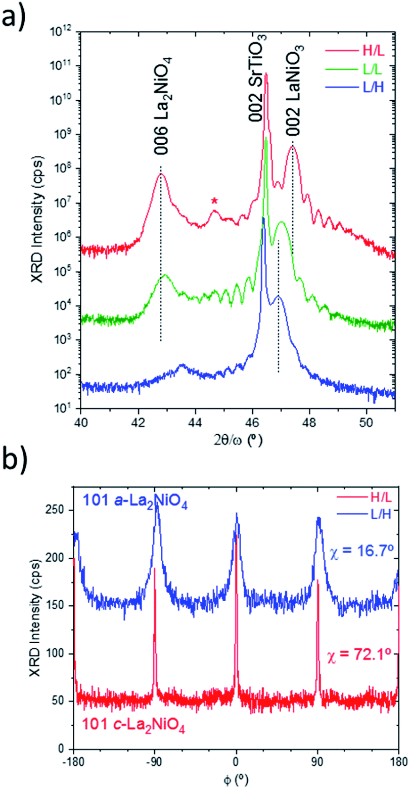 | ||
| Fig. 1 (a) High resolution X-ray diffraction 2θ/ω scans in the vicinity of 002 SrTiO3 substrate reflection of the three bilayer samples combination of the growth at low and high pO2. The peaks labelled as 006 La2NiO4 and 002 LaNiO3 correspond to c-axis oriented domains. Note that the weak 006 La2NiO4 peak in the L/H sample is due to the dominant a-axis orientation of this layer. (The peak with * corresponds to a double-crystal diffraction and is an indication of high crystal coherence of the whole bilayer) (b) ϕ-scans of the 101 La2NiO4 reflections indicating either dominant out-of-plane c-orientation or a-orientation of the La2NiO4 film, for the extreme H/L and L/H samples, respectively. | ||
| Sample | pO2 (mTorr) | LaNiO3c-parameter (Å) | La2NiO4c-parameter (Å) | La2NiO4 orientation |
|---|---|---|---|---|
| Bilayer (LaNiO3/La2NiO4) | 70/10 (H/L) | 3.832 | 12.664 | Pure c⊥ |
| 10/10 (L/L) | 3.862 | 12.637 | Mixed c⊥ and a⊥ | |
| 10/70 (L/H) | 3.870 | — | Pure a⊥ | |
| Single layer | 10 (L) | 3.877 | 12.632 | Pure c⊥ |
| 70 (H) | 3.830 | 12.686 | Pure c⊥ |
The LaNiO3c-parameter values are consistent with the results obtained for the single layers, as shown also in Table 1, (the corresponding XRD patterns are in the supplementary part: Fig. S2 and S3†) in the sense that the lattice parameters measured for films grown in low pO2 are expanded (about 1%) with respect to those obtained at high pO2. This can be explained by a larger oxygen vacancy concentration, as expected for LaNiO3−δ. The crystal quality of the LaNiO3 layer is preserved at both pO2.
However, when comparing the cell parameter values of LaNiO3 in the single layer deposited at low pO2 with those obtained in the bilayers at the same conditions, a slight reduction of the cell parameter between 0.2–0.4% is observed. This reduction has been observed regardless of the pO2 used during the growth of the subsequent La2NiO4 layer. This means that LaNiO3 deposited at low pO2 oxidizes during the deposition of La2NiO4 (either at low or high pO2), while it maintains a constant oxygen content when deposited at high pO2. This is consistent with the observed oxygen transport previously reported in LaNiO3/La2NiO4 bilayers at elevated temperatures,15 although, a possible effect of the impinging energy of the growing species to scavenge oxygen vacancies from the underlying LaNiO3 cannot be discarded.16,17 Therefore, the LaNiO3 layers deposited at low pO2 (L/L and L/H bilayers) could potentially develop an oxygen vacancy gradient at the interface with La2NiO4. A different situation occurs for the La2NiO4 layers. At low pO2 a clear c-axis orientation is observed for La2NiO4 (for the H/L and L/L bilayers), with an intense 006 reflection for both films. The c-axis parameter for the L/L samples is about 12.64 Å, similar to that obtained for La2NiO4 single layers directly grown on the SrTiO3 substrate (Fig. S3† and Table 1) for the same pO2 conditions.
This could be another indication of a certain oxygen ion transport happening between the LaNiO3 and La2NiO4 layers. However, in this case it could not be ruled out that part of the changes in La2NiO4 cell parameter are due to a different strain when growing on LaNiO3 instead of directly on SrTiO3 substrates.
When growing La2NiO4 at high pO2, in the L/H bilayer, no 006 reflection is observed. Therefore, this La2NiO4 film does not present domains with c-axis orientation, contrary to single La2NiO4 films which showed c-axis orientation when directly grown on SrTiO3 substrates (Fig. S2†). This type of scan does not preclude the existence of other orientations of La2NiO4, i.e. a-axis orientation, which would overlap with the intense substrate peaks. In order to clarify whether La2NiO4 grows with a different orientation Φ-scans of asymmetric reflections, such as 101 La2NiO4, were performed at a sample stage tilt angle χ = 16.7°, which is the position expected for the a-oriented domains, as depicted in Fig. 1b. Indeed, the scan over the L/H sample shows the presence of broad 101 peaks with 4-fold symmetry. This indicates the existence of a-axis orientation with perfect in-plane alignment with the substrate [100]/[010] directions. For comparison, the corresponding Φ-scan of the 101 reflection for the c-axis oriented domains in the H/L sample, in this case at χ = 72.1°, was also measured indicating again a four-fold symmetry with a large degree of in-plane arrangement. Therefore, the growth of La2NiO4 at high pO2 promotes the growth of a-axis domains, while c-axis orientation is obtained at low pO2.
This situation was different to the direct growth of La2NiO4 on SrTiO3(001) substrates where a high degree of c-axis orientation is achieved at both pO2 values (Fig. S3†). Therefore, it is likely that the exposure of underlying LaNiO3 to the high pO2 before the subsequent growth of La2NiO4 affects the LaNiO3 topmost surface to inhibit the perfect cube-on-cube arrangement of perovskite blocks of c-axis oriented La2NiO4 on LaNiO3. In agreement with the La–Ni–O thermodynamic phase diagram,2 it is possible that some secondary phases, resulting from LaNiO3 decomposition into La2NiO4 + NiO are also present at the interface, which could alter the subsequent growth of La2NiO4.
Fig. 2 shows the cross-sections oriented along [100]-zone axis at the interface between bottom LaNiO3 and top La2NiO4 layers for the three different deposition conditions: H/L (top), L/L (middle), and L/H (bottom). The left column shows HRTEM images of the bilayers where clear differences in microstructure are revealed in top and bottom layers. All the bilayers show highly oriented LaNiO3 with a large density of vertical planar defects, which very likely correspond to Ruddlesden–Popper type defects, a sort of antiphase boundary defect with a displacement of half primitive perovskite cell along the 〈111〉 direction, as previously shown in.18,19
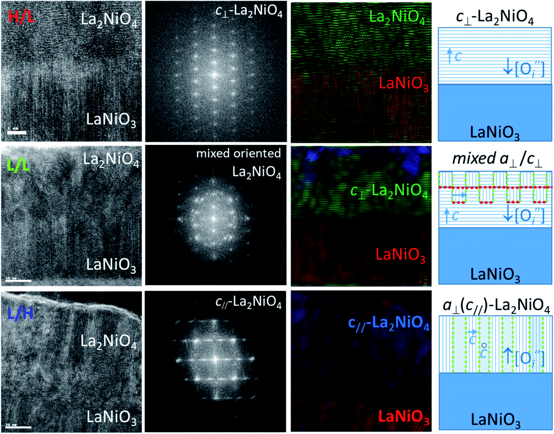 | ||
Fig. 2 HRTEM images (left column) of cross sections of the different bilayers from top to bottom: H/L, L/L and L/H LaNiO3/La2NiO4 bilayers, as well as corresponding FFT patterns of the La2NiO4 layer (second column). The third column shows colour-filtered images for the selected spots in the FFT corresponding to cubic perovskite (red), c⊥-Ruddlesden–Popper (RP) (green), a⊥-RP (blue). The column on the right shows a schematic of the film's microstructure and domain orientation (the c-axis is indicated with blue arrows) for the three types of samples, showing the formation of boundaries between a⊥- and c⊥-domains: perpendicular (marked in red colour) and parallel (green) to the vertical axis. It also shows the high concentration or low concentration of oxygen interstitials ( ) in the initial state depending on the deposition conditions. ) in the initial state depending on the deposition conditions. | ||
On the other hand the nano-structural differences of the La2NiO4 films of the bilayers are more pronounced. The H/L sample shows a sharp interface with highly c-axis oriented La2NiO4. The corresponding FFT of the top La2NiO4 layers are shown in the second column in Fig. 2. For the H/L sample the pattern is consistent with a pure c⊥-orientation, and a- or b- axis parallel to the image, aligned with in-plane main [100]/[010] substrate directions. For the L/L sample, the first layers at the interface with LaNiO3 start growing with c⊥-orientation, but after 5–8 nm additional domains with a different orientation start to nucleate, resulting in a FFT which consists of a mixture of c⊥- and a⊥-orientations. The existence of a c⊥-component was already observed in the XRD pattern of this film. However, the existence of a mixed a⊥-orientation was not detected because of the overlap with the substrate peaks. For the L/H bilayer the majority of the La2NiO4 film seems to be formed by narrow columns of a⊥-oriented domains, some of them with the c-axis parallel to the image (c//). This orientation is identified at atomic scale by the arrangement of bright vertical atomic planes corresponding to the a/b plane of the Ruddlesden–Popper structure, while other domains do not show such contrast, presumably because in this case the c-axis lays perpendicular to the image. The corresponding FFT is consistent with pure a⊥-orientation, as already shown by the ϕ-scans in Fig. 1b. The third column of Fig. 2 corresponds to colour-filtered images obtained by selecting the spots in the FFT for either LaNiO3 phase (red), c⊥-La2NiO4 (green) and a⊥ (c//)-La2NiO4 (blue). The H/L sample shows full c⊥-La2NiO4 (full green colour), while the L/L sample shows mixed c⊥- and a⊥- La2NiO4 (green with blue patches). The L/H sample shows a columnar arrangement with an intimate mixture of blue and red stripes, with nanometer size domains, corresponding to a⊥-La2NiO4. The red stripes correspond in this case to a⊥-La2NiO4 domains with c-axis pointing perpendicular to the image, which are not distinguished from a standard perovskite structure (red colour), but obviously do not correspond to LaNiO3 although they show the same FFT pattern. The right column in Fig. 2 summarizes these observations in the form of a schematic of the samples' microstructures. The regions where La2NiO4 domains with different orientation meet together form grain boundaries. In the pure c⊥-axis oriented film (H/L) there are not grain boundaries in the La2NiO4 layer, whereas in the mixed a⊥/c⊥-oriented La2NiO4 layer (in the L/L sample) there are vertical and horizontal (001)/(100) boundaries between a⊥ and c⊥ domains. In the pure a⊥ La2NiO4 layer (in the L/H sample) the in-plane rotation by 90° of their corresponding c-axis defines also vertical (001)/(100) domain boundaries. The vertical and horizontal domains have been marked with green and red colours, respectively, in Fig. 2 (right column).
To conclude this section, different growth conditions (pO2) induce remarkable differences not only in the oxygen concentration profiles across the bilayer, with possible gradients at the LaNiO3−δ/La2NiO4+δ interface, but also in the bilayer nano-structure, with the appearance of a particular type of (001)/(100) grain boundaries within La2NiO4. These differences will surely affect the electrical properties of these bilayers and could ultimately dictate the memristive behaviour of Pt/LaNiO3/La2NiO4/Pt devices, as will be discussed in the following section.
Role of the pO2 on the electrical properties of Pt/LaNiO3/La2NiO4/Pt memristive devices
Fig. 3 presents an overview of the electrical response of the three bilayers using circular Pt contacts with a diameter of 200 μm. The voltage was applied to the Pt electrodes directly on top of LaNiO3 bottom layer (bright part of the image in Fig. 3a), while the Pt contacts on top of La2NiO4 (dark side of Fig. 3a) were grounded, as shown in the schematic of Fig. 3b. The shape of each voltage sweep cycle versus time is depicted in Fig. 3c. The I(V) measurements were reproducible when cycling within a fixed voltage range.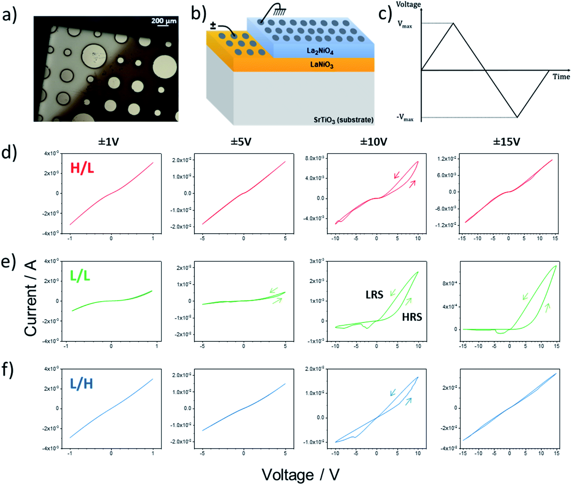 | ||
| Fig. 3 (a) Optical image of the top surface of the Pt/LaNO3/La2NiO4/Pt sample showing the circular Pt electrodes. (b) Schematic of the measuring configuration from grounded top Pt electrode on the La2NiO4 layer to biased Pt electrode on the LaNiO3 bottom layer. (c) Applied triangular voltage sweeps. (d)–(f) Evolution of the I(V) characteristics of the H/L, L/L and L/H bilayers, respectively, when increasing the maximum voltage from left to right (±1 V, ±5 V, ±10 V and ±15 V). The L/L sample shows clear analog-type switching characteristics. (Arrows indicate the direction of the voltage sweep). | ||
The I(V) curves measured for the three samples are shown in Fig. 3d–f, corresponding to every fifth cycle at the ±1 V, ±5 V, ±10 V and ±15 V sweeps. Interface-type memristive devices typically show rectifying I–V characteristics in their initial resistance state (IRS). This nonlinear behaviour is usually explained by the presence of a Schottky-like barrier at the metal/oxide interface necessary for the emergence of the memristive behavior.5 Both the H/L and the L/L samples show nonlinear I(V) characteristics in their IRS (I–V sweeps between ±1 V). Since Pt forms an ohmic contact with both LaNiO3 and La2NiO4 (as shown in Fig. S4†) the nonlinearity can only be explained by the presence of a Schottky-like barrier at the LaNiO3/La2NiO4 complex-oxide interface. The increased nonlinearity measured for the L/L sample could signify the presence of a larger Schottky barrier. On the other hand the L/H sample shows almost linear I(V) characteristics between ±1 V and should therefore present the smallest LaNiO3/La2NiO4 contact resistance. As will be later explained, this difference is likely due to the high electronic conductivity expected for the La2NiO4 top layer of the L/H sample due to its a⊥ orientation, high oxygen overstoichiometry (δ) and concomitant high concentration of electronic hole carriers.
Other interesting differences can be noticed between the samples when increasing Vmax gradually from ±1 V to ±15 V. Both the HRS and the LRS for all three samples present some form of hysteresis which is most pronounced at Vmax = ±10 V. It should be noticed that the small hysteretic behavior disappears when Vmax is increased to ±15 V for the H/L and L/H samples, as clearly shown in the resistance versus voltage plots in Fig. S5.† The disappearing of the hysteresis seems to be irreversible as the subsequent application of a lower voltage does not restore the original opening in two resistance states (not shown here). On the other hand the L/L sample progressively shows an increasingly rectifying behaviour with two very distinct resistance states. The Low Resistance State (LRS – higher current branch), shows little rectification within the ±2 V sweeping range, i.e. before the devices switches to the High Resistance State (HRS). Conversely, the HRS shows highly rectifying I(V) characteristics with an increased threshold voltage when compared to the LRS. This hysteretic behavior and the distinct LRS and HRS states are well maintained even for the largest voltage sweep range (±15 V). The evolution of the HRS and LRS values (measured at 500 mV immediately after each sweep) as well as the corresponding HRS/LRS ratios are shown in Fig. S6† for the three bilayer samples. For the H/L and L/H samples both the HRS and LRS show very low values (<103 Ω) below Vmax = ±7 V. For larger voltage sweep ranges, in the H/L sample both states increase to values up to 104 Ω, while for the L/H sample they remain relatively low. However, in both cases the HRS/LRS ratios stay between 1 and 3 for the whole measured range. Interestingly the L/L sample shows a completely different behaviour where both the HRS and LRS values continuously increase all the way from the lowest values of Vmax = ±1 V until Vmax = ±15 V. At Vmax = ±7 V, the LRS reaches a stable value of around 104 Ω, while the corresponding HRS continues increasing above 105 Ω. Therefore, the corresponding HRS/LRS ratio shows a pronounced increase from 1–2 below Vmax = ±7 V up to 20–30 at Vmax = ±15 V.
Focusing on the LaNiO3/La2NiO4 interface we interpret the resistive switching behavior based on the mixed ionic-electronic conducting character of La2NiO4+δ, and its anisotropy, and we present two possible scenarios or mechanisms which can explain the observed memristance. The layered Ruddlesden–Popper structure of La2NiO4+δ is expected to induce a high anisotropy both in the electronic transport and oxygen diffusion properties.10–13 At room temperature the resistivity along the c-axis was measured to up to three orders of magnitude larger than that within the basal plane,12,13 mainly attributed to differences in mobility due to the variation in interplanar separation within the crystallographic structure. In addition, as a p-type conductor, the resistivity highly depends on the oxygen content, and more particularly to the interstitial oxygen content, which is directly related to the concentration of electronic hole carriers. We recently showed that for epitaxial La2NiO4+δ thin films prepared by Pulsed Injection Metal Organic Chemical Vapor Deposition, we could easily change the oxygen interstitial concentration by annealing in different gas atmospheres (from H2/Ar to O2), leading to changes in the c-axis out of plane cell parameter from 12.62 to 12.69 Å.9 The resistivity values of the different films showed three orders of magnitude increase in resistivity (from 5.3 × 10⁻³ to 5.7 Ω cm) when decreasing the oxygen content (smaller cell parameter). Thus, in the case of the L/H sample studied here a higher electronic conductivity is expected across the top La2NiO4+δ film due to: (i) an increased oxygen content (compared to the other two samples) leading to a larger hole carrier concentration, and (ii) its a⊥-orientation (opposite to the other samples), and thus along the fastest electronic transport path in this anisotropic material. This could significantly reduce the carrier depletion width on the La2NiO4+δ side of the interface Schottky contact, therefore reducing the overall contact resistance. Consequently, this prevents the building up of a memristive behavior in this bilayer (small HRS/LRS ratio at Vmax = ±10 V that then disappears at higher voltages).
In the following we focus only on the H/L and L/L samples which, do present a Schottky-like characteristics and present the first potential mechanism. Besides the drift of highly mobile electronic charges, typically forming a depletion zone at the interface, in a material such as La2NiO4+δ the application of an external electrical field above a certain voltage facilitates the drift of charged oxygen defects (negatively-charged interstitial oxygen,  , in this case).10 Then, the accumulation of oxygen interstitials at the interface with LaNiO3 may produce a change in the Schottky barrier as well as in the material properties in this location, which result in a change in the contact resistance and ultimately in the overall resistance of the device. Indeed, in the L/L sample, that shows the largest memristive behavior, a strong nonlinearity was observed at low voltage, probably caused by this potential barrier. The resistance-change mechanism in Pt/LaNiO3/La2NiO4/Pt could therefore be explained as follows: initially, the device is in a HRS. When applying a high enough positive voltage (on the LaNiO3 side) the negatively-charged oxygen ions drift towards the LaNiO3/La2NiO4 interface, locally changing the carrier density (the mobile interstitial oxygen ions,
  , act as hole dopants in La2NiO4) and reducing the charge depletion width in this location. The device now finds itself in its LRS as the flow of current is now facilitated through a thinner potential barrier (additional conduction mechanisms can be present, i.e. tunneling). The opposite occurs when applying a high enough negative voltage. Oxygen interstitials in La2NiO4 drift away from the LaNiO3/La2NiO4 interface reestablishing the barrier width, and therefore the HRS.
Although, in the previous explanation, the oxygen interstitial accumulation region has been limited to the La2NiO4 part at the interface with LaNiO3, a possible exchange of oxygen ions between the LaNiO3−δ and the La2NiO4+δ layers, may result in an extension of the depletion region through an internal redox mechanism, also modifying the contact resistance. This corresponds to the second mechanism proposed. This recombination at the interface of LaNiO3−δ and the La2NiO4+δ layers has been observed at 600 °C by Moreno et al.,15 and it is likely that the exchange of oxygen ions between the two materials can occur at room temperature, assisted by the electric field and by Joule heating. Finally, it is possible that the two mechanisms evoked previously are cohabitating, both playing a role in the measured change in resistance of the device.
While the hysteretic behavior is much more pronounced for the L/L bilayer, the comparison of the film's microstructure between H/L and the L/L samples, as observed by HRTEM and depicted in the schematic in Fig. 2, does not reveal any relevant difference at the LaNiO3/La2NiO4 interface itself. Both bilayers show sharp interfaces between c⊥-LaNiO3 and c⊥-La2NiO4 layers across the entire interfacial region. However, the differences in their respective LaNiO3 and La2NiO4 cell parameters seem to indicate a variation in their corresponding oxygen defect concentrations, higher  concentration in the LaNiO3 side for the L/L sample (larger cell parameter, see Table 1) and higher
  concentration in the La2NiO4 layer for the H/L sample (larger cell parameter, see Table 1). The reduced concentration of
  within LaNiO3 in the H/L sample, is expected to limit the amount of oxygen ions that can be incorporated into LaNiO3 (from the La2NiO4 film) and their drift within the film towards the Pt electrode. This could be one of the reasons for the smaller HRS/LRS ratios measured for this sample compared to the L/L sample. The second main difference between these two bilayers is found in the nano-structure of the top part of the La2NiO4 film. A mixed orientation of the La2NiO4 domains in the L/L sample generates a high density of (001)/(100) boundaries within the La2NiO4 layer. It is likely that these internal (001)/(100) nano-domain boundaries form additional barriers, effectively blocking both electronic and ionic drift particularly those boundaries laying perpendicular to the electric field (red colour in the schematic presented in the right column of Fig. 2), and therefore, accumulating traps in the volume of the La2NiO4 layer. If the presence of these domain boundaries helps increasing the rectifying and hysteretic I(V) characteristics, this could bring an additional strategy for engineering film microstructures with enhanced and better controlled memristive properties.
Conclusions
High crystal quality preferentially oriented LaNiO3/La2NiO4 bilayers were grown using PLD under varying pO2 conditions. The results confirmed that the oxygen partial pressure used during the growth of the films clearly impacts their microstructure, severely affecting the domain orientation of the La2NiO4 layer. At the same time electrical measurements carried out on Pt/LaNiO3/La2NiO4/Pt devices fabricated out of these bilayers confirmed important pO2-dependent differences in the resistive switching behavior of these complex-oxide stacks. Two switching scenarios have been proposed to explain the memristive behavior of the bilayers. The proposed mechanisms could be occurring independently or simultaneously, depending on the voltage range. While the first one has been attributed to the electric field-induced drift of oxygen interstitial ions in the La2NiO4 layer, accumulating at the LaNiO3/La2NiO4 interface, and modulating the depletion width of the Schottky barrier present; the second one would be related to the exchange of oxygen ions between the top La2NiO4 and the bottom LaNiO3 films. This study also reveals the presence of a high density of boundaries between domains with c⊥ and a⊥-orientation, under particular film growth conditions, which could also play a significant role in the accumulation of oxygen interstitials in the volume of the La2NiO4 layer, possibly improving the memristive properties of these novel bilayer nickelate-based devices.Author contributions
Conceptualization: KM, MB and JS; thin film deposition: CW, JMCR, VL; TEM analysis: BB, formal electrical characterisation: CW, KM; writing –review & editing: KM, MB, JS.Conflicts of interest
There are no conflicts to declare.Acknowledgements
This work has been financed by the ANR funded project “MICROSWITCH” (ANR-14-ACHN-0012) and by the “FUN-TO-BE” CNRS-CSIC supported International Program for Scientific Cooperation (PICS, no. PICS07294). Part of this work was carried out through the access to PLD and HRTEM facilities granted by the NFFA-Europe Infrastructure (proposal ID 886) under Horizon 2020 EU Funding Program. JS acknowledges the grant PID2019-108573GB-C21 funded by MCIN/AEI/10.13039/501100011033. This work was also supported in part by the Spanish Ministry of Economy, Industry and Competitiveness (projects MAT2016-77100-C2-1-P), and by the Catalan AGAUR agency (project: 017-SGR-579). ICN2 is funded by the CERCA programme/Generalitat de Catalunya and by the Severo Ochoa programme (SEV-2017-0706).References
- I. Riess, Solid State Ionics, 2003, 157, 1–17 CrossRef CAS.
- J. A. Kilner and M. Burriel, Materials for intermediate-temperature solid-oxide fuel cells, 2014, vol. 44 Search PubMed.
- C. Lenser, R. Dittmann and J. P. Strachan, in Resistive Switching, Wiley-VCH Verlag GmbH & Co. KGaA, Weinheim, Germany, 2016, pp. 437–456 Search PubMed.
- C. Baeumer, T. Heisig, B. Arndt, K. Skaja, F. Borgatti, F. Offi, F. Motti, G. Panaccione, R. Waser, S. Menzel and R. Dittmann, Faraday Discuss., 2019, 213, 215–230 RSC.
- K. Maas, E. Villepreux, D. Cooper, C. Jiménez, H. Roussel, L. Rapenne, X. Mescot, Q. Rafhay, M. Boudard and M. Burriel, J. Mater. Chem. C, 2020, 8, 464–472 RSC.
- K. Maas, E. Villepreux, D. Cooper, E. Salas-Colera, J. Rubio-Zuazo, G. R. Castro, O. Renault, C. Jimenez, H. Roussel, X. Mescot, Q. Rafhay, M. Boudard and M. Burriel, Adv. Funct. Mater., 2020, 30, 1909942 CrossRef CAS.
- A. Aguadero, J. A. Alonso, M. J. Martínez-Lope, M. T. Fernández-Díaz, M. J. Escudero and L. Daza, J. Mater. Chem., 2006, 16, 3402–3408 RSC.
- A. Chroneos, D. Parfitt, J. A. Kilner and R. W. Grimes, J. Mater. Chem., 2010, 20, 266–270 RSC.
- J. M. Bassat, P. Odier, A. Villesuzanne, C. Marin and M. Pouchard, Solid State Ionics, 2004, 167, 341–347 CrossRef CAS.
- M. Burriel, G. Garcia, J. Santiso, J. A. Kilner, R. J. Chater and S. J. Skinner, J. Mater. Chem., 2008, 18, 416–422 RSC.
- M. Burriel, H. Téllez, R. J. Chater, R. Castaing, P. Veber, M. Zaghrioui, T. Ishihara, J. A. Kilner and J.-M. Bassat, J. Phys. Chem. C, 2016, 120, 17927–17938 CrossRef CAS.
- J. M. Bassat, F. Gervais, P. Odier and J. P. Loup, Mater. Sci. Eng., B, 1989, 3, 507–514 CrossRef.
- J. M. Honig and D. J. Buttrey, in Localization and Metal-Insulator Transitions, Springer US, Boston, MA, 1985, pp. 409–418 Search PubMed.
- T. Yu, Y. F. Chen, Z. G. Liu, X. Y. Chen, L. Sun, N. Ben Ming and L. J. Shi, Mater. Lett., 1996, 26, 73–76 CrossRef CAS.
- R. Moreno, P. García, J. Zapata, J. Roqueta, J. Chaigneau and J. Santiso, Chem. Mater., 2013, 25, 3640–3647 CrossRef CAS.
- J. Zhu, J.-W. Lee, H. Lee, L. Xie, X. Pan, R. A. De Souza, C.-B. Eom and S. S. Nonnenmann, Sci. Adv., 2019, 5, eaau8467 CrossRef CAS PubMed.
- E. Mikheev, B. Hoskins, D. Strukov and S. Stemmer, Nat. Commun., 2014, 5, 3990 CrossRef CAS PubMed.
- E. Detemple, Q. M. Ramasse, W. Sigle, G. Cristiani, H.-U. Habermeier, B. Keimer and P. A. van Aken, J. Appl. Phys., 2012, 112, 013509 CrossRef.
- S. Bagdzevicius, M. Boudard, J. M. Caicedo, X. Mescot, R. Rodríguez-Lamas, J. Santiso and M. Burriel, Solid State Ionics, 2019, 334, 29–35 CrossRef CAS.
Footnote |
| † Electronic supplementary information (ESI) available. See DOI: 10.1039/d1ta10296f |
| This journal is © The Royal Society of Chemistry 2022 |