
 Open Access Article
 This Open Access Article is licensed under a
 Creative Commons Attribution 3.0 Unported Licence
Nanoscale metal oxides–2D materials heterostructures for photoelectrochemical water splitting—a review
Ananta R.
Fareza
 a,
Ferry Anggoro Ardy
Nugroho
*b,
Fatwa F.
Abdi
*c and
Vivi
Fauzia
*a
a,
Ferry Anggoro Ardy
Nugroho
*b,
Fatwa F.
Abdi
*c and
Vivi
Fauzia
*a
aDepartment of Physics, Universitas Indonesia, Depok 16424, Indonesia. E-mail: vivi@sci.ui.ac.id
bDepartment of Physics and Astronomy, Vrije Universiteit Amsterdam, De Boelelaan 1081, 1081 HV Amsterdam, the Netherlands. E-mail: ferryanggoroardynugroho@yahoo.com
cInstitute for Solar Fuels, Helmholtz-Zentrum Berlin für Materialien und Energie GmbH, Berlin, 14109, Germany. E-mail: fatwa.abdi@helmholtz-berlin.de
First published on 23rd March 2022
Abstract
Photoelectrochemical (PEC) water splitting is an interesting approach to harness clean and renewable solar energy to generate green hydrogen. To this end, metal oxides (MOs) have been investigated as photoelectrodes (photoanode and photocathode) due to their tunable optoelectronic properties and abundance, but achieving an efficient overall performance based on single MOs is very challenging due to their narrow visible light absorption, unfavorable band position, low charge mobilities, and limited stability. Heterostructuring MOs with other materials has therefore been proposed in the literature. In this review, we specifically highlight photoelectrodes based on the heterostructure of MOs and an emerging group of 2D materials consisting of mono elemental (Xenes), carbides/nitrides/carbonitrides (MXenes), boron carbon nitride (BCNs), transition metal dichalcogenides (TMDs), metal–organic frameworks (MOFs), and bismuth oxyhalides (BiOX). The benefits of the formation of MOs/2D materials heterostructures are outlined, and the state-of-the-art of MOs/2D materials heterostructures as photoelectrodes with various architectures are extensively discussed. Finally, a critical outlook on fundamental challenges and potential future directions in the development of MOs/2D materials heterostructures is presented.
 Ananta R. Fareza | Ananta R. Fareza received his BS degree in Physics from Universitas Indonesia in 2018. Afterwards, he obtained his MS degree in Materials Science from the same institution under the supervision of Dr Vivi Fauzia and Dr Ferry Anggoro Ardy Nugroho in 2022. His research interests are in the material development and characterization of photoelectrochemical water splitting and supercapacitor. |
 Ferry Anggoro Ardy Nugroho | Ferry Anggoro Ardy Nugroho is a Marie Skłodowska-Curie Postdoctoral Fellow in Vrije Universiteit Amsterdam, the Netherlands. He holds a Bachelor degree from Nanyang Technological University, Singapore, a Master degree in Nanoscience and Nanotechnology from KU Leuven, Belgium and Chalmers University of Technology, Sweden, and a PhD in Materials Science also from Chalmers University of Technology. His works on plasmonic alloy hydrogen sensors won him Graduate Student Awards from European Materials Research Society and the Arne Sjögren's Prize for Most Innovative Thesis in Nanoscience and Nanotechnology. His research interest includes materials science, nanofabrication, nanoplasmonics and optics, and sensor technologies. |
 Fatwa F. Abdi | Fatwa Abdi is a group leader and the deputy head of the Institute for Solar Fuels, Helmholtz-Zentrum Berlin. He obtained his Bachelor degree from NTU, Singapore, and Master's degree from NUS, Singapore, and MIT, USA, all in Materials Science. After a short stint in the semiconductor industry, he completed his PhD in Chemical Engineering (cum laude) at TU Delft, the Netherlands, in 2013. He was the recipient of the Martinus van Marum prize from the Royal Dutch Society of Sciences and Humanities. His research focuses on the development of novel materials and engineering of devices for solar energy conversion applications. |
 Vivi Fauzia | Vivi Fauzia received her Bachelor's and Master's degrees in Physics (1995 & 1997) from Institut Teknologi Bandung, Indonesia and she completed her Ph.D. from Institute of Microengineering and Nanoelectronics (IMEN) Universiti Kebangsaan Malaysia in 2013. Currently, she is an Assistant Professor at the Department of Physics, Universitas Indonesia. Her research interest currently focuses on 2D materials for photodetection, photothermal water evaporation and clean energy generation applications. |
Introduction
The global energy demands have been constantly increasing and are predicted to reach 30–50 terawatts by 2050. Fulfilling this demand with the status-quo condition is worrying since nearly 83% of today's global energy supply is still based on fossil fuels, such as natural gas, petroleum, and coal.1 The primary byproduct from burning these fuels is CO2, the gas that makes up almost 76% of the annual greenhouse gas emissions.2 Over the past decades, these emissions have significantly increased and severely threatened the environment and public health, resulting in e.g., diminishing coral reefs due to ocean warming, flooded coastal cities, deadly heatwaves, strong hurricanes, intensified droughts, wildfires, and air pollution.3–6 These situations call for urgent exploration of alternative fuels that are environmentally sustainable and commercially viable.Hydrogen is one promising alternative to satisfy current and future energy demands due to its high gravimetric energy density compared to other fuels (Fig. 1)7, making it attractive for various applications. For example, for applications as transport fuels (i.e., in vehicles), hydrogen can be reacted with ambient oxygen using fuel cells to produce electricity with water as the only byproduct. In another context, hydrogen is also an important feedstock in the production of many value-added chemicals (e.g., ammonia, hydrocarbon, pharmaceuticals). However, hydrogen production is not without challenges. Apart from its low volumetric energy density (Fig. 1), hydrogen is not readily available in nature (despite being the most abundant element in the universe) and thus requires additional steps to produce. Nearly 96% of the hydrogen produced worldwide is derived from fossil fuels,8,9 namely steam methane reforming, naphtha reforming, and coal gasification, while only 4% originates from renewable sources, such as photo/dark fermentation,10,11 thermochemical pyrolysis,12 and water electrolysis.8 In the effort to increase the latter portion, extensive research is done to further advance the sustainable routes to become cost-competitive with the fossil-fuel based ones. To this end, water electrolysis requires a thermodynamic potential of 1.23 V and some kinetic overpotential (0.4–0.6 V). To minimize the dependency on electricity in such a system, new approaches have been proposed. Among several options, photoelectrochemical (PEC) water splitting stands out as an attractive method13–17 because it relies on an identical mechanism, but with the thermodynamic and kinetic potential being supplied by sunlight, and it can be constructed using inexpensive semiconductors. On average, the sun illuminates the earth's surface with ∼23![[thin space (1/6-em)]](https://www.rsc.org/images/entities/char_2009.gif) 000 TWy annually;18 a tremendous value compared to the annual worldwide energy demand of ∼20 TWy in 2019.19 Together with the maturing development in fuel cells, the large-scale implementation of green hydrogen energy in households, transportations, and industrial manufacturing is expected in the near future.
000 TWy annually;18 a tremendous value compared to the annual worldwide energy demand of ∼20 TWy in 2019.19 Together with the maturing development in fuel cells, the large-scale implementation of green hydrogen energy in households, transportations, and industrial manufacturing is expected in the near future.
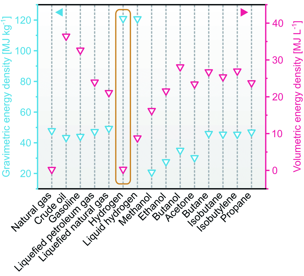 | ||
| Fig. 1 Gravimetric and volumetric energy densities of various fuels based on the lower heating value (LHV). Data is adapted from ref. 7. | ||
In the quest for high solar-to-hydrogen conversion, decades of research have devised several PEC architectures from single20–22 to tandem photoelectrodes,13,23 including hybridization with buried photovoltaics system, with the current record of 19.3% demonstrated STH efficiency.24 Complementarily, the exploration of materials for improved PEC water splitting is an active research endeavor. To this end, several classes of materials have been studied, namely III–V group compounds,25 organic semiconductors,26 and metal oxides (MOs).27 Apart from its low-cost,28 MOs particularly display tunable optoelectronic properties through facet-,29 morphology-,30 and defects engineering,31 which are favorable for PEC water splitting. MOs are also easy to synthesize through, e.g., solvo-/hydrothermal,32 electrodeposition,33 spray pyrolysis,34 sol–gel,35 radio frequency sputtering,36 chemical vapor deposition,37 pulsed laser deposition,38 atomic layer deposition,39 and molecular beam epitaxy.40 Despite the rising number of PEC water splitting works based on single MOs (Fig. 2), major problems related to limited visible light absorption, unfavorable band position, low charge mobilities, and self-degradation are inherent, resulting in low overall STH efficiency. Additionally, the generated photovoltage in a single MOs is rather limited; even high-grade semiconductors have only achieved photovoltages <70% of the band gap (Eg).41 Employing a single MO as a photoelectrode in a PEC water splitting has thus been considered unlikely. To address these problems, one can establish a heterostructure device with other materials of complementary properties. Among them, hybridizing MOs with two-dimensional (2D) materials presents several advantages. 2D materials are a group of novel materials that recently emerged in energy storage and conversion applications due to their distinct thickness-dependent optoelectronic properties,42,43 large surface areas,44 and enormous experimental charge mobilities.45,46 Thus, MOs/2D materials heterostructures offer a promising alternative for durable implementation toward affordable and sustainable hydrogen generation. Consequently, in the past decade, the number of published research articles related to MOs- and 2D materials-based PEC water splitting in the literature is steadily increasing (Fig. 2).
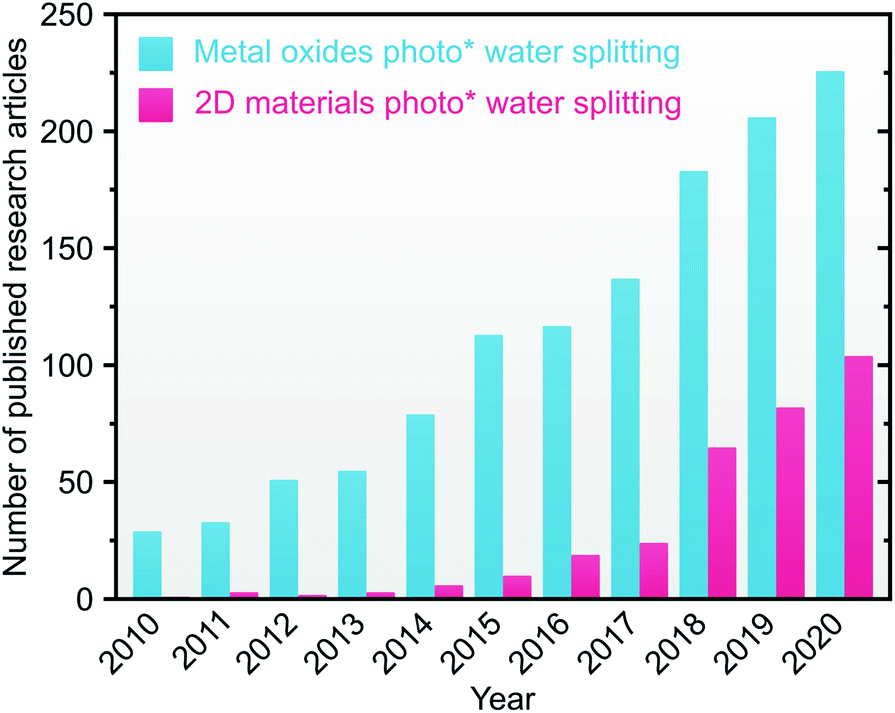 | ||
| Fig. 2 The number of published research articles indexed at Scopus related to PEC water splitting based on metal oxides and 2D materials. The search strings used were ‘metal oxides photo* water splitting’ and ‘2D materials photo* water splitting.’ Accessed on 25 September 2021. | ||
Acknowledging this rising attention and emerging research direction, in this review we summarize the state-of-the-art of PEC water splitting employing nanoscale MOs/2D materials heterostructures. To provide a solid background into the topic, we first focus on the fundamentals of PEC water splitting, including a discussion on its common performance characterizations. Second, we highlight the materials requirements for PEC water splitting, which emphasize the need to establish a heterostructure device, specifically using MOs/2D materials composites. We then in detail recapitulate the latest progress in PEC water splitting using different types of MOs/2D materials heterostructures. Finally, we identify related future challenges and provide our outlook for further development in the field.
Fundamentals of PEC water splitting
PEC water splitting comprises two chemical surface reactions: (i) water oxidation or oxygen evolution reaction (OER), and (ii) water reduction or hydrogen evolution reaction (HER). PEC water splitting is a thermodynamically uphill reaction with a Gibbs free energy (ΔG°) of 237.2 kJ mol−1,17 with the following net reaction| 2H2O → 2H2 + O2 | (1) |
A PEC water splitting device is made of a semiconductor as the working electrode paired with a metal electrode as the counter electrode (Fig. 3a). The semiconductor serves as either a photoanode for OER (Fig. 3b) or a photocathode for HER (Fig. 3c). Due to the respective position of the Fermi level after equilibrium, an n-type material is generally required as a photoanode, while a p-type as a photocathode. These electrodes are immersed in an electrolyte containing a redox species and are illuminated by sunlight. Mechanistically, PEC water splitting comprises three subsequent steps, namely band gap excitation, charge separation and transfer, and surface reaction.
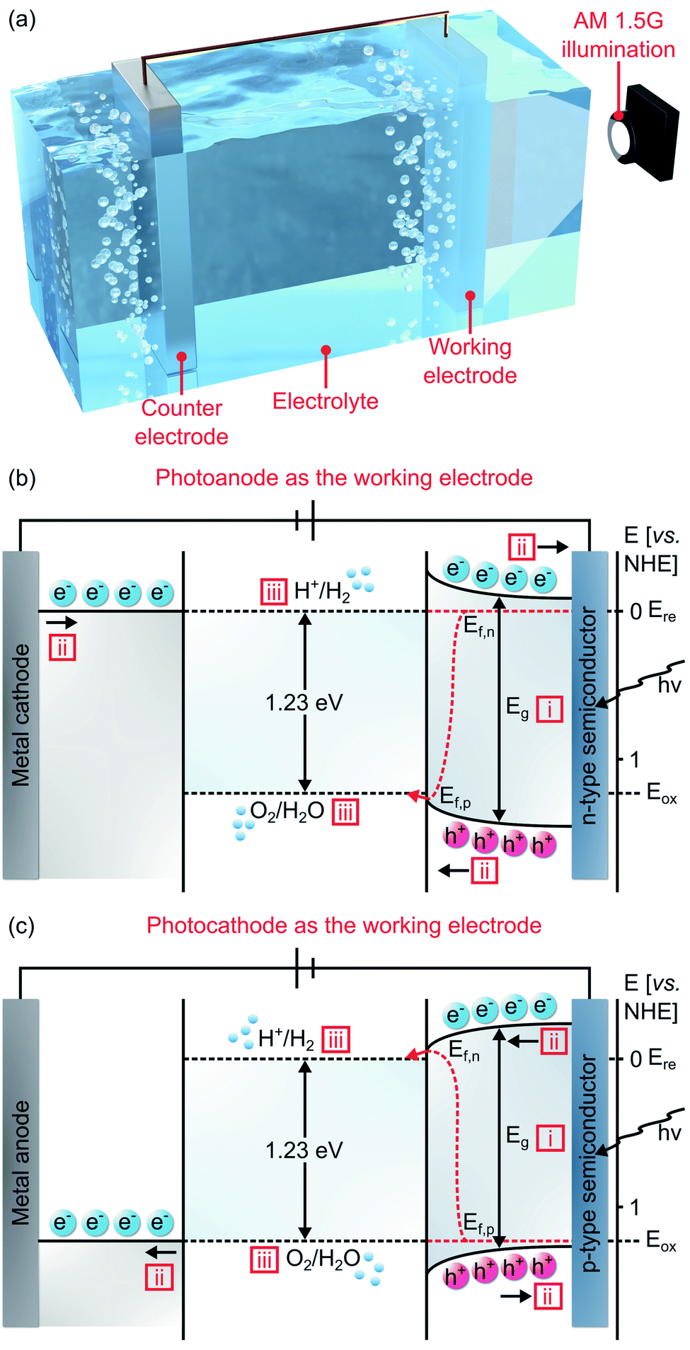 | ||
| Fig. 3 (a) An artist's rendition of a basic PEC water splitting components comprising of a working electrode and a counter electrode immersed in an electrolyte with AM 1.5G illumination as a light source. Three steps of overall PEC water splitting in (b) photoanode and (c) photocathode: (i) Eg excitation, (ii) charge separation and transfer, (iii) surface reactions of OER and HER. | ||
When a semiconductor is irradiated with photons of energies (hν) higher than the semiconductor Eg, electrons are excited from the valence band (VB) to the conduction band (CB), leaving holes in the VB.16 Conceptually, Eg defines the number of charges that can be excited by incoming photons with targeted wavelength range. Eg, VB, and CB are optoelectronic properties that depend on the electronic structure of the semiconductors. Downsizing a semiconductor into the nanoscale would alter its band structure due to the quantum confinement effect, where decreasing particle size increases the Eg and vice versa.47–49 Furthermore, optical scattering is likely to be increased by nanoscale semiconductors; if the nanoscale structure is properly engineered, the optical pathway in the semiconductor and the corresponding absorption can thus be increased.
Next, the photogenerated electrons and holes oppositely migrate to the surface of the photocathode and the photoanode, respectively.50 In an n-type photoanode, holes are the minority charge carriers, which move to the surface of the photoanode to perform OER.51 Conversely, electrons, as the majority charge carriers in an n-type photoanode, migrate to the p-type photocathode through an external wire.51 Similarly, accumulated electrons in the p-type photocathode flow into the surface of the photocathode to execute HER. The separate movements of the charge are determined by the electric field in the depletion region and the selectivity at the semiconductor and electrolyte interface, with high mobility signifying a fast charge transport.50 Since excited electrons have a short lifetime, it is crucial for them to migrate toward the surface of the photoelectrode to further participate in surface reactions. Thus, a swift charge transport is preferable. Unfortunately, several semiconductors suffer from low charge mobility. One technique to tackle low charge mobilities is via nanostructuring, where the shortened diffusion length facilitates a rapid charge transport from the interior to the surface of the photoelectrode, hence minimizing charge recombination rate. An efficient charge transport resulting from establishing a heterostructure can also mitigate self-oxidation/reduction due to excessive charge carriers.52 However, nanostructuring also poses a negative impact by shrinking the depletion region that is beneficial for charge separation, as the thickness of a depletion region is limited by the size of the semiconductor.49
Finally, the surface reaction OER occurs on the photoanode, while HER does on the photocathode. The reaction rate is largely dependent on the active catalytic surface area. One strategy to increase the reaction rate is therefore by engineering the photoelectrode's architecture into the nanoscale.53 At the same time, mass transport of ions from the nanoscale surface to the bulk of the electrolyte (and vice versa) may be limited. Diffusion in porous media (e.g., nanostructure) is expected to be slower than that in the bulk electrolyte. Accumulation and/or depletion of ions could therefore be an issue with nanoscale photoelectrodes and result in additional overpotential. On the other hand, it has been reported that the produced gas bubbles are transported away more efficiently with rough electrodes, as shown experimentally in the case of Si microwire photoelectrodes.54 Nanoscale electrodes are therefore expected to show this effect, which can be further improved by increasing the surface wettability, including the formation of superhydrophilic and/or superaerophobic surface55,56 and the introduction of material porosity.55
In a PEC water splitting, when referring to the normal hydrogen electrode (NHE) potential, the values of water reduction potential (Ere) and water oxidation potential (Eox) are 0 V and 1.23 V, respectively.17,57 Consequently, a theoretical Eg of 1.23 eV in a semiconductor is necessary to thermodynamically split water into oxygen and hydrogen. In addition, kinetic overpotentials are needed to sustain the reactions. The OER overpotential in an n-type semiconductor photoanode is defined as the gap between the quasi-Fermi level of holes (Ef,p) to the Eox, while the HER overpotential in a p-type semiconductor photocathode is referred to as the gap between the quasi-Fermi level of electrons (Ef,n) to the Ere (Fig. 3).58 As a result, to achieve a low additional electrical bias, the OER and HER overpotentials should be kept minimum. Considering the overpotential (0.4–0.6 eV) and thermodynamic energy losses during the interfacial charge transfer due to possible mismatch (0.3–0.4 eV), the actual driving voltage for water splitting reaction is higher than 1.23 V, known as the photovoltage.58 Therefore, it has been identified that the ideal Eg for PEC water splitting is ∼2.0 eV (equivalent to light absorption at ∼620 nm).16,58,59 This finding is also in mutual agreement with the fact that the majority (43%) of the solar radiation energy is within the visible range (380–740 nm).60 Under Air Mass 1.5 Global (AM 1.5G) illumination at 100 mW cm−2, a semiconductor with a 2.0 eV Eg can reach a maximum photocurrent density of 14.5 mA cm−2 and theoretical solar-to-hydrogen efficiency of 17.9%.59
As novel materials for PEC water splitting emerge, standardized efficiency measurements and parameters need to be strictly regulated. This guidance ensures that efficiency measurements coming from a broad scientific community is properly catalogued and comparable. Typically, the illumination source is standardized to simulate the intensity of 1 sun (100 mW cm−2). Meanwhile, the selection of the electrolyte is rather loosely stipulated due to the disparate stability of various materials within a particular range of electrolyte's pH. For more details, the readers are directed to excellent reviews and book chapters on standardized protocols for PEC measurements.58,61,62
Efficiency calculations in PEC water splitting
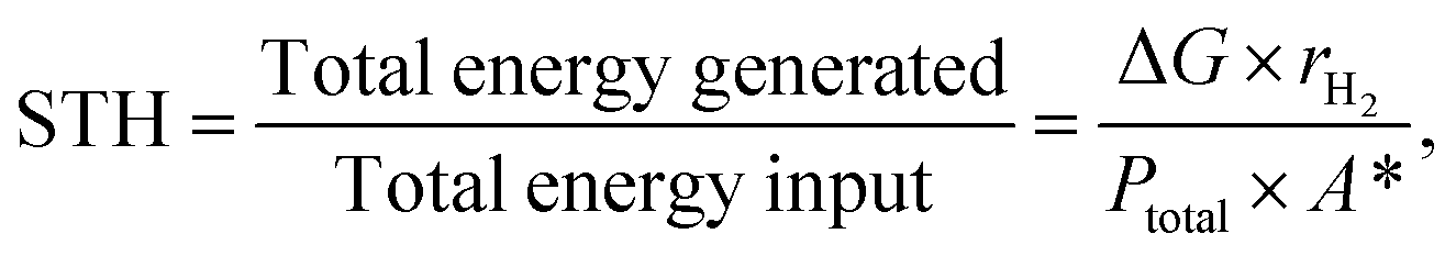
Efficiency calculations in a PEC water splitting device provide a quantitative information about the system's capability to split water into oxygen and hydrogen in the presence of sunlight. There are three types of efficiencies based on how they are measured, solar-to-hydrogen (STH) efficiency, applied bias photon-to-current efficiency (ABPE), and incident photon-to-current efficiency (IPCE). Ideally, all of these values should be disclosed when reporting a PEC water splitting device (unless they are unattainable due to certain conditions).The STH efficiency is defined as the ratio of the chemical energy of the produced hydrogen to the solar energy input58 and serves as a comparative value from one device to another since it reflects the true ability of semiconductors when used in a PEC water splitting device at 1 sun or 100 mW cm−2. An extra care has to be done when calibrating the lamps used as solar simulators in the laboratories to prevent over- or underestimations of the efficiency values.63,64 The equation to calculate the STH efficiency is
 | (2) |
Due to several conditions (e.g., unfavored band position or extensive charge recombination), some semiconductors fail to generate photocurrent without an applied bias. Applying an external bias between two electrodes requires a new type of efficiency since the situation no longer translates the true ability of materials in performing PEC water splitting: the ABPE.16 This efficiency is calculated using
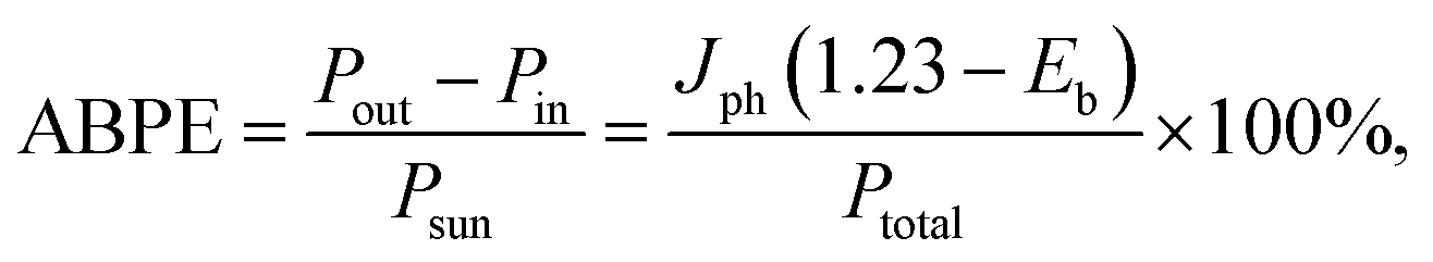 | (3) |
Last, the ratio of photogenerated charge carriers relative to the measured photocurrent per incident photon as a function of wavelength or energy of monochromatic light is defined as the IPCE. It measures how efficient the semiconductors are in generating charge carriers under a single wavelength, including optical loss factors in transmission and reflection. IPCE measurement is typically performed at a particular applied potential and can be determined as
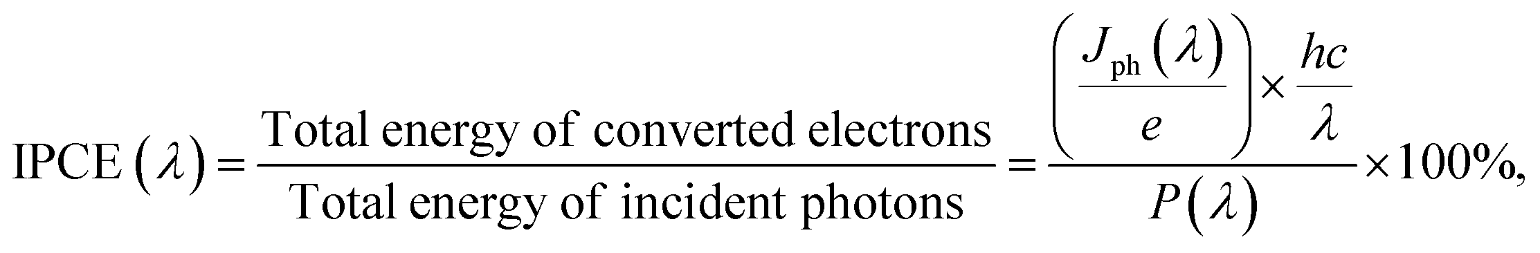 | (4) |
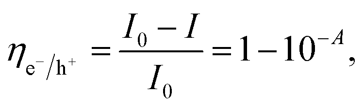
| IPCE(λ) = ηe−/h+ × ηseparation × ηtransfer. | (5) |
 | (6) |
Having discussed all the efficiencies above, STH is the most appropriate value in correctly benchmarking the PEC water splitting devices under strict conditions. However, other efficiencies of ABPE, and IPCE can be considered diagnostic efficiencies and are also beneficial in the development and characterization of materials for PEC water splitting.
Materials selection for photoelectrochemical water splitting
As a reminder, PEC water splitting can be achieved by accomplishing three steps: charge photogeneration, the separation and transfer of the photogenerated charge, and the participation of electrons and holes to the surface reactions of HER and OER, respectively. Consequently, each of these three steps need to be considered carefully when selecting effective materials for PEC water splitting to maximize the overall performance. Below, we discuss the different material aspects that are taken into account and have been implemented using individual MOs and 2D materials, and their composites.Metal oxides
MOs is a group of inorganic semiconductors comprising metal atoms that bind to oxygen atoms. They have distinct physicochemical properties, including structure, morphology, and optoelectronics. Furthermore, MOs are robust, easy-to-synthesize, and cost-effective materials, which are attractive for low-cost applications. For instance, some of the most commonly used metal oxides are composed of Fe, Zn and Ti, which were globally produced as much as ∼3000, 12 and 5 million tonnes per year, respectively, according to the World Mineral Production.28 Thus, MOs have become one of the most prevalent materials in photogenerated charge separation and conversion applications, such as in hydrogen production via PEC water splitting,66 CO2 reduction,67 pollutant degradation,68 and anti-microbial properties.69Over the past decades, numerous binary MOs have been studied extensively for PEC water splitting. These include ZnO,70,71 α-Fe2O3,72,73 Cu2O,74,75 TiO2,76,77 SnO2,78,79 MoO3,71,80 WO3,81,82 and V2O5.83,84 Besides that, ternary MOs of, for example, BiVO4,21,85 Bi2MoO6,80,86 Bi2WO6,87,88 CuWO4,22,89 and ZnFe2O4,90,91 have also emerged as viable options. However, finding the best performing MOs for PEC water splitting is not without challenges. Many MOs typically exhibit a wide Eg, resulting in a narrow light absorption range that limits the generation of charge carriers. For example, ZnO, TiO2, SnO2, and NiO have Eg in the range of 3.2–3.6 eV. Although the wide Eg may provide sufficient photovoltage for PEC water splitting, it limits light absorption within the UV range, which only contributes ∼5% to solar spectrum.60 To this end, several MOs also exhibit visible-sensitive Eg, such as α-Fe2O3 (2.1 eV), Cu2O (2.2 eV), MoO3 (2.2 eV), WO3 (2.7 eV), V2O5 (1.9 eV), and BiVO4 (2.4 eV), to name a few.
In general, the VB of MOs lies well below Eox (since it is typically dominated by O-2p orbitals), but only a few that display higher CB than Ere (e.g., ZnO, NiO, Cu2O, and TiO2). This limitation means that many MOs are only sufficient for the OER half reaction, but not for the HER due to unfavorable CB position. The CB of MOs is typically governed by the s- and d-metal orbitals with a strong overlap of electrons clouds, while the VB comprises largely localized p-oxygen orbitals.92 In general, MOs have low charge mobilities caused by low crystallinity and high defects density, such as oxygen vacancy,93 that act as impurity scattering centers, resulting in high charge recombination.94 Besides that, due to the ionic nature of the lattice, charge carriers in MOs create polarons by displacing atoms in the vicinity. This phenomenon lowers the energy of the carriers and traps them within the potential well.95 Hence, MOs yield low-to-moderate charge mobilities from 0.05 to 300 cm2 V−1 s−1 depending on the measurement conditions.83,85,96,97
The redox ability of MOs is also determined by their metal activity, which is defined as the ability of metals to be oxidized by releasing electrons during a redox reaction. Typically, metal activity decreases as the element goes to the bottom left portion of the periodic table. For example, Zn is more reactive compared to Fe. OER kinetics in MOs is also generally sluggish owing to faster holes migration toward the solid/liquid interfacial area compared to holes injection rate into the electrolyte.16,98 This condition results in holes accumulation and further intensifying charge recombination rate. MOs also have a tendency to be self-reduced and/or self-oxidized by accumulative charge depending on their respective self-reduction and self-oxidation potentials compared to the Ere and Eox.52 On top of that, photogenerated carriers of MOs have a short lifetime of pico- to nanoseconds to participate in OER and HER,99 that also contributes to high charge recombination. It is also noteworthy that electrolyte pH affects the stability of MOs during PEC measurements. For instance, TiO2 displays high stability in harsh conditions in both acidic and alkaline environments,100 while NiO shows high stability only within high pH.101
2D materials
2D materials have become the center of interest in the past decade due to their exceptional characteristics,44,102–105 following the first successful attempt to experimentally synthesize graphene in 2004.106 This group of materials can be further divided based on their Eg: metals or semi-metals (∼0 eV), semiconductors (<4 eV), and insulators (>4 eV). Interestingly, a number of 2D materials exhibit thickness-dependent Eg modulation.42,43 In particular, their bulk form has an indirect Eg, while its monolayer counterpart yields a slightly wider and direct Eg.107 2D materials also offer large interface areas to hold surface reactions while being extremely thin, thus establishing shorter charge transfer pathways.50 This is in contrast with 1D materials, where they depend on the anisotropic longitudinal shape to transfer the photogenerated charge efficiently. These wide ranges of physicochemical properties offer high versatility for widespread and practical applications, including energy conversions and energy storages,108,109 environmental remediations,110 optoelectronics,111 and electronics.112 To this end, there are several subgroups of 2D materials based on their compositions: mono elemental (Xenes), carbides/nitrides/carbonitrides (MXenes), boron carbon nitrides (BCNs), transition metal dichalcogenides (TMDs), metal–organic frameworks (MOFs), and bismuth oxyhalides (BiOX), as shown in Fig. 4.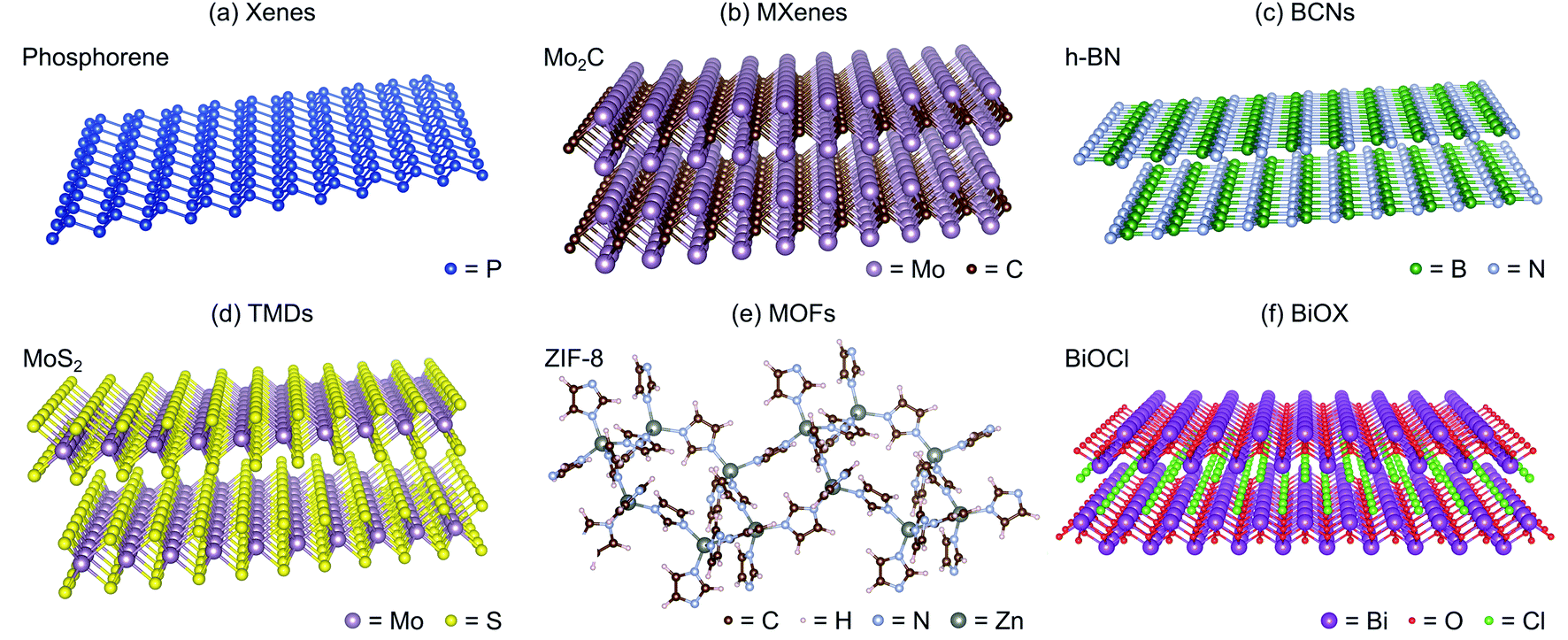 | ||
| Fig. 4 Representative 2D materials family categorized by their compositions. (a) Phosphorene of Xenes, (b) Mo2C of MXenes, (c) h-BN of boron carbon nitrides (BCNs), (d) MoS2 of transition metal dichalcogenides (TMDs), (e) ZIF-8 of metal–organic frameworks (MOFs), and (f) BiOCl of bismuth oxyhalides (BiOX). | ||
Finally, it is noteworthy that 2D materials should not exist above the absolute zero (the lowest limit of the thermodynamic temperature scale, 0 K) based on the theoretical framework.113 Thus, 2D materials are not perfectly flat and exhibit intrinsic ripples with the bending factor of the plane proportional to the temperature.114 At room temperature, 2D materials may experience lattice distortion and make them appear like crumpled 3D materials. For instance, a typical graphene sheet at room temperature forms wrinkles with a height displacement of 0.7 Å.114 Throughout this review, several authors report 2D materials with the appearance or morphology of non-conventional layered structures (e.g., 0D or 3D). Nevertheless, they are still considered as 2D materials as per the definition, and this is also the classification we use here.
A common feature of 2D materials is that multiple repeating layers are held together by weak van der Waals (vdW) forces to establish bulk crystals. One can exfoliate 2D materials to obtain mono-to-few layers by, for example, mechanical cleavage,115 strain engineering,116 and sonication,117 that lead to higher exposed catalytically active sites.104 The high surface areas of 2D materials provide substantial photoreactive sites for both light absorption and surface reactions. However, several studies have suggested that the edges are chemically more active than the basal planes.118–120 This is rather unfortunate because the ratio between basal planes to edges is typically high (i.e., basal planes are more exposed than the edges). The difference in catalytic activity between these two sites accommodates carrier delocalization and diffusive transport along the interface areas as an effect of non-hybridized atomic orbitals of the 2D materials. These effects result in higher charge mobilities in the in-plane (edges) in contrast to the out-of-plane (basal planes) surface.121 However, the activation of basal planes to be catalytically active is also possible by covalent functionalization,122 defects engineering,123 hydrogenation,124 or electron beam direct surface patterning.125 This activation is advantageous since charge carriers do not have to travel far to the edge sites to participate in the reaction, and thus the probability for charge recombination can be minimized. Furthermore, 2D materials also exhibit enormous experimental charge mobilities, e.g., graphene (∼350000 cm2 V−1 s−1),45 phosphorene (∼4000 cm2 V−1 s−1),46 and MoS2 (∼200 cm2 V−1 s−1),126 that is beneficial for fast charge transfer across the material.
2D materials, however, also possess significant drawbacks related to restacking and layer overlapping because of the lack of interfacial interactions.127,128 Therefore, the experimental surface areas, specifically the active sites, are typically lower than the calculated ones. One way to avoid such problem is by forming a heterostructure system with, e.g., MOs. In this case, 2D materials can serve as co-catalysts by enhancing MOs merit for PEC water splitting. To this end, co-catalysts based on 2D materials have shown promising potentials in such heterostructure architecture to improve light absorption and electrons and holes separation,129,130 to provide additional active sites for surface reactions,131,132 and to increase durability against photocorrosion.133
As a result, one major research direction in PEC water splitting is routed toward establishing composite heterostructure devices to mitigate the above problems. On the one hand, 2D materials with narrow Eg, such as phosphorene (1.5 eV), MoS2 (1.3 eV), MoSe2 (1.4 eV), offer excellent visible light absorption. In addition, various types of heterostructures can be formed owing to diverse CB and VB positions as summarized in Fig. 5. For example, PbS is one emerging 2D material for photocathode due to its narrow Eg and advantageous CB position,134 whereas BiOI can flexibly act as photoanode or photocathode owing to its favorable CB and VB positions for HER and OER, respectively.66,135
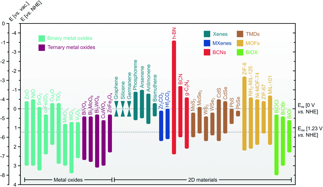 | ||
| Fig. 5 Representative Eg and band positions of MOs and 2D materials. Upper and lower horizontal dashed lines represent Ere of 0 V vs. NHE and Eox of 1.23 V vs. NHE, respectively. | ||
Metal oxides/2D materials heterostructures
Forming a heterostructure by integrating 2D materials and MOs can be an elegant solution in tackling the weaknesses of MOs for PEC water splitting discussed above (i.e., narrow light absorption, short charge lifetime, high charge recombination rate, and poor structural stability under specific pH). Specifically, nanoscale MOs-2D materials heterostructures provide advantageous aspects for PEC water splitting in five ways. First, although nanoscale MOs provide significantly higher surface area compared to their bulk counterparts, they tend to agglomerate into larger clusters with decreased surface area.136,137 Here 2D materials can be used as an immobilization platform where MOs are dispersed throughout their surfaces. Agglomeration can thus be reduced with the increasing surface interactions between MOs and 2D materials. Second, the energetic misalignment (CB, VB positions, Fermi level EF) between MOs and 2D materials can be engineered to enhance photogenerated charge separation. Hence, the lifetime of charge carriers can be prolonged as electrons and holes are spatially isolated. Third, the lattice mismatch, formed at the interface between MOs and 2D materials,121,138,139 may introduce interfacial strains that could contribute to Eg tuning.140,141 This provides an alternative route to optimize the light absorption range. Fourth, 2D materials that possess high aqueous stability can be used as a protective layer for unstable MOs, thus preventing the structural decomposition of MOs.133 Finally, these two materials can play different roles that synergistically work to enhance the performance of a PEC water splitting. Notably, the majority of MOs act as photoactive materials, while 2D materials can serve as photoactive and/or catalytic-active materials. Photoactive 2D materials can absorb light, which in turn increase the amount of electrons and holes pair. Furthermore, they may boost the surface reaction as catalysts by reducing the corresponding activation energy. On the other hand, non-photoactive 2D materials do not interact with light and thus only serve as catalysts. Combining these two materials together into a heterostructure may result in a photoelectrode with good light absorption while maintaining high catalytic activity compared to their isolated counterparts.76Another consideration when forming a composite is related to the heterostructure type. To this end, there are four types of heterostructures that are categorized based on their charge transfer mechanism: type I, type II, p–n junction, and Z-scheme (Fig. 6). In a type I heterostructure, the CBMin and VBMax of material 1 (M1) straddle those of material 2 (M2), such that photogenerated electrons and holes move simultaneously from M1 into M2 and potentially recombine in M2 (Fig. 6a).142 Conversely, the CB and VB of M1 are both higher than those of M2 in type II heterostructures; photogenerated electrons transfer from M1 to M2, while the holes move oppositely from M2 to M1 (Fig. 6b).142 This spatial separation of electrons and holes typically is considered to be beneficial in reducing charge recombination. When the type II heterostructures are composed of p-type and n-type semiconductors, a p–n junction is formed. Electrons in the n-type semiconductor diffuse into the p-type and holes in the p-type diffuse oppositely into the n-type and further to form a built-in electric field for improving charge separation (Fig. 6c).143 Finally, a Z-scheme heterostructure has the same band alignment as type II, although the charge transfer mechanism is slightly different because of the different types of interface (i.e., Schottky instead of ohmic). The photogenerated electrons in M1 and holes in M2 are spatially confined and do not move into the other semiconductor, while the photogenerated electrons in M2 recombine with the holes from M1 (Fig. 6d).143 These confined charge carriers can reduce the steric hindrance that contributes to the detrimental effect on the performance.144 To this end, one can validate the formation of Z-scheme instead of type II using several methods, as discussed elsewhere.145 It is worth noting that type II, p–n junction, and Z-scheme heterostructures are favorable for PEC water splitting since all of them provide better charge separation and transfer compared to that in type I.142,146
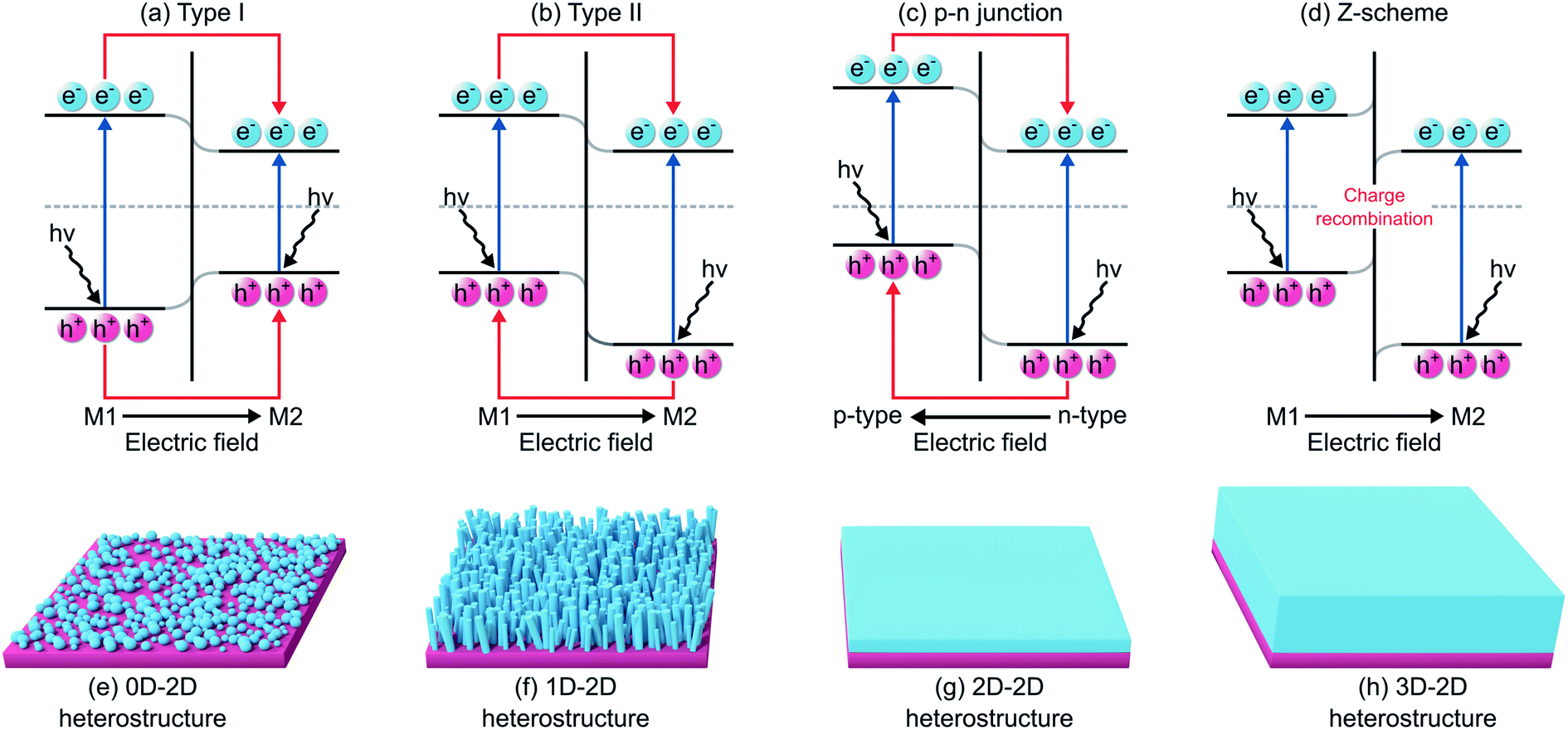 | ||
| Fig. 6 Possible (a–d) charge transfer mechanisms throughout the heterostructure interface areas and (e–h) different types of heterostructures with various mixed-dimensionality. In panel (a–d), M1 and M2 are material 1 and material 2, respectively, while the blue and red lines represent band gap excitation and charge transfer at the interface, respectively. | ||
Besides the charge transfer mechanism, heterostructures can also be divided based on their respective dimensionality. The main focus here is 2D materials, which exhibit no chemical bonding between each stacking layer and no dangling bonds on their surfaces.139 Therefore, they offer flexibility when combining with MOs without the constraint in lattice mismatch.121,138 Heterostructures based on 2D materials are termed vdW heterostructures. There are four types of vdW heterostructures: 0D–2D (Fig. 6e), 1D–2D (Fig. 6f), 2D–2D (Fig. 6g), and 3D–2D (Fig. 6h) heterostructures. It is also noteworthy that 2D materials can be synthesized into lower dimensionality forms, e.g., quantum dots (0D) of Ti3C2Tx,147 h-BN,82 and MoS2.148 These novel heterostructures of mixed dimensionality have unfolded numerous possibilities in widespread applications, such as light-emitting diodes,149 photovoltaics,150 photodetectors,151 field-effect transistors,152 and solar energy conversion.72,153 There are wide options of 2D materials to establish MOs/2D materials heterostructures: Xenes, MXenes, BCNs, TMDs, MOFs, and BiOX. In the following sections, we will discuss each group of these heterostructures thoroughly, where an exhaustive summary of their performances as photoanode and photocathode is presented in Tables 1 and 2, respectively.
| Materials | Charge transfer mechanisma | vdW heterostructure typeb | OER onset potentialc (V vs. RHE) | J ph at 1.23 V vs. RHE (mA cm−2) | η separation at 1.23 V vs. RHE (%) | η transfer at 1.23 V vs. RHE (%) | IPCE at 400 nm (%) | Electrolyte | Light intensity (mW cm−2) | Ref. |
|---|---|---|---|---|---|---|---|---|---|---|
| a Unclear charge transfer mechanism arises from heterostructures that use non-semiconductor 2D materials. b In some works, the 2D materials form other lower dimensionality structures, e.g., quantum dots (0D). c Various onset potentials and reference electrodes are converted into values vs. RHE using Nernst equation. | ||||||||||
| ZnO/g-C3N4 | Type II | 1D–2D | 0.1 | 0.7 | N.A. | N.A. | N.A. | 0.1 M Na2S + 0.2 M Na2SO3 | 70 | 154 |
| ZnO/MoS2 | Type II | 1D–2D | 0.4 | 2.0 | N.A. | N.A. | N.A. | 0.5 M Na2SO4 | 100 | 71 |
| ZnO/CdSe | Type II | 1D–0D | −0.1 | N.A. | N.A. | N.A. | 20.4 | 0.2 M Na2S | 100 | 155 |
| ZnO/CdSe | Type II | 1D–0D | 0.2 | 2.8 | N.A. | N.A. | N.A. | 0.4 M Na2S + 0.3 M K2SO3 | 100 | 156 |
| ZnO/γ-In2Se3 | Type II | 1D–0D | −0.1 | 3.5 | N.A. | N.A. | N.A. | 0.3 M Na2S + 0.4 M Na2SO3 | 100 | 157 |
| SnO2/g-C3N4 | Type II | 1D–0D | 0.3 | 1.9 | N.A. | N.A. | N.A. | 0.1 M NaOH | 100 | 79 |
| SnO2/CdS | Type II | 3D–1D | −0.1 | 3.8 | N.A. | N.A. | 42.0 | 0.3 M Na2S + 0.4 M Na2SO3 | 100 | 158 |
| α-Fe2O3/g-C3N4 | Type II | 3D–0D | 1.0 | 0.4 | N.A. | 22.0 | N.A. | 0.5 M Na2SO4 | 100 | 159 |
| α-Fe2O3/CdS | Type II | 1D–0D | 0.5 | 3.0 | N.A. | N.A. | N.A. | 1.0 M NaOH + 0.1 M Na2S | 100 | 160 |
| TiO2/g-C3N4 | Type II | 1D–2D | 0.2 | 0.9 | N.A. | N.A. | N.A. | 0.1 M Na2SO4 | 100 | 161 |
| TiO2/MoS2 | Type II | 3D–2D | 0.1 | 0.6 | N.A. | N.A. | N.A. | 1.0 M NaOH | 100 | 162 |
| TiO2/MoSe2 | Type II | 3D–2D | 0.1 | 0.9 | N.A. | N.A. | N.A. | 1.0 M NaOH | 100 | 77 |
| TiO2/PbS | Type II | 1D–0D | 0 | 1.2 | N.A. | N.A. | N.A. | 0.1 M Na2S + 0.2 M Na2SO3 | 100 | 163 |
| TiO2/PbS | Type II | 1D–0D | 0.2 | N.A. | N.A. | N.A. | 18.0 | 0.1 M Na2S | 90 | 164 |
| TiO2/CdS | Type II | 1D–0D | 0.1 | 1.9 | N.A. | N.A. | N.A. | 0.3 M Na2S + 0.4 M Na2SO3 | 100 | 165 |
| TiO2/CdS | Type II | 3D–0D | −0.3 | N.A. | N.A. | N.A. | 47.4 | 0.3 M Na2S + 0.4 Na2SO3 | 100 | 166 |
| TiO2/CdSe | Type II | 1D–0D | −0.5 | 1.5 | 14.3 | N.A. | 13.0 | 0.3 M Na2S + 0.4 Na2SO3 | 100 | 167 |
| WO3/g-C3N4 | Type II | 2D–0D | 0.8 | 0.7 | N.A. | N.A. | 40.0 | 0.2 M Na2SO4 | 100 | 81 |
| WO3/MoS2 | Type II | 2D–0D | 0.6 | 1.0 | N.A. | N.A. | 15.0 | 0.5 M H2SO4 | 100 | 148 |
| WO3/CdS | Type II | 1D–0D | 0.4 | 1.0 | 90.0 | 49.0 | N.A. | 0.2 M Na2SO4 | 100 | 131 |
| WO3/BiOI | Type II | 3D–2D | 0.7 | 1.2 | N.A. | N.A. | 22.5 | 0.5 M Na2SO4 | N.A. | 168 |
| BiVO4/g-C3N4 | Type II | 3D–3D | 0.4 | 4.1 | N.A. | 64.9 | 60.0 | Mixed phosphate buffer | 100 | 169 |
| BiVO4/CdS | Type II | 2D–0D | −0.2 | 6.6 | N.A. | N.A. | 39.0 | 0.5 M Na2SO3 | 100 | 170 |
| BiVO4/BiOCl | Type II | 1D–2D | 0.8 | 0.7 | 25.0 | 52.0 | N.A. | 0.5 M Na2SO4 | 100 | 171 |
| Bi2MoO6/g-C3N4 | Type II | 2D–2D | 0.8 | 0.4 | N.A. | N.A. | 1.8 | 0.1 M Na2SO4 | N.A. | 86 |
| Bi2MoO6/CdS | Type II | 2D–0D | 0.7 | 0.8 | N.A. | N.A. | 27.0 | 0.2 M Na2SO4 | 100 | 172 |
| CuWO4/CdS | Type II | 3D–0D | 0.2 | N.A. | N.A. | N.A. | 27.0 | 0.1 M Na2SO4 | 100 | 173 |
| ZnFe2O4/CdS | Type II | 0D–1D | 0.1 | 2.0 | N.A. | N.A. | 14.0 | 0.4 Na2S + 0.3 M Na2SO3 | 100 | 90 |
| ZnO/MoS2 | p–n junction | 1D–2D | 0.4 | 1.2 | N.A. | N.A. | N.A. | 0.5 M Na2SO4 | 100 | 174 |
| ZnO/PbS | p–n junction | 1D–2D | 0.7 | 12.0 | N.A. | N.A. | N.A. | 0.1 M Na2SO4 | 100 | 175 |
| NiO/g-C3N4 | p–n junction | 2D–2D | 1.2 | 0.1 | N.A. | N.A. | N.A. | 0.1 M KOH | N.A. | 176 |
| TiO2/BiOCl | p–n junction | 1D–2D | −0.4 | 0.3 | N.A. | N.A. | 26.0 | 0.5 M Na2SO4 | 100 | 177 |
| BiVO4/black phosphorus | p–n junction | 3D–2D | 0.6 | 1.7 | 95.8 | 33.0 | N.A. | 0.5 M KPi | 100 | 178 |
| BiVO4/MoS2 | p–n junction | 3D–2D | 0.3 | 3.0 | 70.0 | 54.0 | 24.0 | Mixed phosphate buffer | 100 | 153 |
| BiVO4/BiOI | p–n junction | 3D–2D | 0.3 | 3.3 | N.A. | 68.8 | 44.0 | 0.5 M KH2PO4 | 100 | 66 |
| CuWO4/BiOI | p–n junction | 0D–2D | 0.6 | 1.5 | 26.0 | 59.6 | 18.0 | Mixed phosphate buffer | 100 | 89 |
| ZnO/graphene | Unclear | 3D–0D | 0.2 | 0.6 | N.A. | 84.0 | 1.8 | 1.0 M NaOH | 100 | 179 |
| ZnO/graphene | Unclear | 1D–2D | 0.4 | 0.3 | N.A. | N.A. | N.A. | 0.5 M Na2SO4 | 150 | 180 |
| α-Fe2O3/rGO | Unclear | 0D–2D | 1.6 | N.A. | N.A. | N.A. | N.A. | 1.0 M NaOH | N.A. | 181 |
| α-Fe2O3/h-BN | Unclear | 1D–0D | 0.7 | 1.1 | 24.0 | 45.0 | N.A. | 1.0 M NaOH | 100 | 182 |
| TiO2/graphene | Unclear | 1D–0D | 0.3 | 0.2 | N.A. | N.A. | 3.8 | 0.5 M Na2SO4 | 100 | 183 |
| TiO2/graphene | Unclear | 1D–0D | 0.8 | 0.4 | N.A. | N.A. | 2.1 | 0.5 M Na2SO4 | 100 | 184 |
| TiO2/rGO | Unclear | 3D–2D | 0.3 | 0.5 | N.A. | N.A. | 2.4 | 1.0 M KOH | 100 | 185 |
| WO3/rGO | Unclear | 0D–2D | 0.8 | 1.1 | N.A. | N.A. | 26.0 | 0.5 M H2SO4 | 100 | 186 |
| WO3/h-BN | Unclear | 2D–0D | 0.8 | 1.6 | 50.0 | 83.0 | 15.0 | 0.1 M Na2SO4 | 100 | 82 |
| BiVO4/rGO | Unclear | 0D–2D | 0.2 | 1.1 | N.A. | N.A. | 32.3 | Mixed phosphate buffer | 100 | 187 |
| BiVO4/Ti3C2Tx | Unclear | 3D–2D | 0.5 | 3.6 | N.A. | 73.0 | 54.0 | 1.0 M K2B4O7 | 100 | 188 |
| Bi2WO6/h-BN | Unclear | 0D–2D | 0.6 | 0.9 | N.A. | N.A. | N.A. | 0.1 M Na2SO4 | N.A. | 88 |
| ZnO/ZIF-8 | Unclear | 1D–2D | 0 | N.A. | N.A. | N.A. | 1.9 | 0.5 M Na2SO4 | 100 | 189 |
| ZnO/ZIF-67 | Unclear | 1D–0D | 0.6 | 1.1 | 52.0 | 75.0 | 0.9 | 0.5 M Na2SO4 | 100 | 190 |
| ZnO/ZnNi-MOF | Unclear | 1D–3D | 0.3 | 1.4 | N.A. | N.A. | N.A. | 0.5 M Na2SO4 | 100 | 70 |
| α-Fe2O3/NH2-MIL-125 | Unclear | 1D–2D | 1.0 | 0.7 | N.A. | N.A. | 45.0 | 1.0 M NaOH | 100 | 191 |
| α-Fe2O3/Ni-MOF-74 | Unclear | 1D–2D | 0.6 | 0.9 | N.A. | 58.0 | 6.2 | 1.0 M KOH | 100 | 73 |
| α-Fe2O3/ZIF-67 | Unclear | 1D–2D | 0.7 | 0.9 | 7.2 | 85.0 | 20.0 | 1.0 M KOH | 100 | 72 |
| α-Fe2O3/MIL-101 | Unclear | 1D–2D | 0.9 | 0.8 | N.A. | N.A. | 20.0 | 1.0 M NaOH | 100 | 192 |
| TiO2/NH2-MIL-125 | Unclear | 1D–2D | 0.4 | 0.8 | 31.7 | 89.2 | 36.0 | 0.5 M Na2SO4 | 100 | 193 |
| TiO2/MIL-100 | Unclear | 1D–2D | 0.4 | 0.8 | N.A. | N.A. | 38.0 | 0.5 M Na2SO4 | 100 | 194 |
| TiO2/NiFe-MOF | Unclear | 1D–2D | 0.3 | 0.8 | 37.4 | 92.8 | 25.0 | 0.5 M Na2SO4 | 100 | 195 |
| BiVO4/Cobim | Unclear | 3D–0D | 0.4 | 3.1 | N.A. | 83.0 | 50.0 | 0.5 M Na2SO4 | 100 | 196 |
| BiVO4/CoNi-MOF | Unclear | 3D–3D | 0.6 | 3.2 | 53.0 | 66.3 | 32.0 | 0.5 M Na2SO4 | 100 | 197 |
| Materials | Charge transfer mechanisma | vdW heterostructure typeb | HER onset potentialc (V vs. RHE) | J ph at 0 V vs. RHE (mA cm−2) | η separation at 0 V vs. RHE (%) | η transfer at 0 V vs. RHE (%) | IPCE at 400 nm (%) | Electrolyte | Light intensity (mW cm−2) | Ref. |
|---|---|---|---|---|---|---|---|---|---|---|
| a Unclear charge transfer mechanism arises from heterostructures that use non-semiconductor 2D materials. b In some works, the 2D materials form other lower dimensionality structures, e.g., quantum dots (0D). c Various onset potentials and reference electrodes are converted into values vs. RHE using Nernst equation. | ||||||||||
| ZnO/BiOBr0.9I0.1 | Type II | 2D–3D | 0.6 | N.A. | N.A. | N.A. | N.A. | Mixed phosphate buffer | N.A. | 198 |
| NiO/g-C3N4 | Type II | 3D–2D | 0.4 | 0 | N.A. | N.A. | N.A. | 0.1 M Na2SO4 | 245 | 199 |
| NiO/CdSe | Type II | 1D–0D | 0.7 | −0.7 | N.A. | N.A. | N.A. | 0.3 M HMT + 0.2 M KCl + 0.1 M HCl | 100 | 200 |
| SnO2/WS2 | Type II | 0D–3D | 0.1 | −3.5 | N.A. | N.A. | N.A. | 0.5 M H2SO4 | N.A. | 78 |
| Cu2O/MoS2+x | Type II | 2D–2D | 0.5 | −5.7 | N.A. | N.A. | N.A. | 0.1 M H2SO4 | 100 | 201 |
| CuO/g-C3N4 | Type II | 3D–2D | 0.6 | −0.5 | N.A. | N.A. | N.A. | 0.2 M KH2PO4 + 0.2 M K2HPO4 | N.A. | 202 |
| MoO3/MoS2 | Type II | 2D–2D | 0.8 | −1.1 | N.A. | N.A. | N.A. | 0.1 M Na2SO4 | 100 | 203 |
| NiO/g-C3N4 | p–n junction | 2D–2D | −0.1 | −6.6 | N.A. | N.A. | N.A. | 0.5 M H2SO4 | N.A. | 176 |
| ZnO/Au/g-C3N4 | Z-scheme | 1D–0D | 0.2 | −0.1 | N.A. | N.A. | 1.5 | 0.2 M Na2SO4 | 100 | 204 |
| Cu2O/graphene | Unclear | 1D–2D | 0.6 | −4.8 | N.A. | N.A. | N.A. | 1.0 M Na2SO4 | 100 | 75 |
| Cu2O/Ti3C2Tx | Unclear | 1D–2D | 0.3 | −4.5 | N.A. | N.A. | 51.0 | 1.0 M Na2SO4 | 100 | 74 |
General synthesis strategies
To this end, there are two classifications of MOs/2D materials heterostructure fabrication route, namely top-down and bottom-up, as summarized in Fig. 7a. Top-down fabrication methods include mechanical exfoliation,106 liquid phase exfoliation,205 and intercalation followed by exfoliation.206 Afterwards, these mono-to-few-layer 2D materials are immersed in a solvent to form a colloidal suspension. This suspension can then uniformly coat MOs using various techniques, including spray-coat, dip-coat, and spin-coat. These methods are compatible with flexible substrates and can be done at room temperature. Recently, Ma et al. fabricated Bi2MoO6/g-C3N4 heterostructure by dip-coating exfoliated g-C3N4 nanosheets colloid onto the surface of Bi2MoO6 nanoarrays for 1 h and annealing at 350 °C for 1 h, as shown in Fig. 7b.86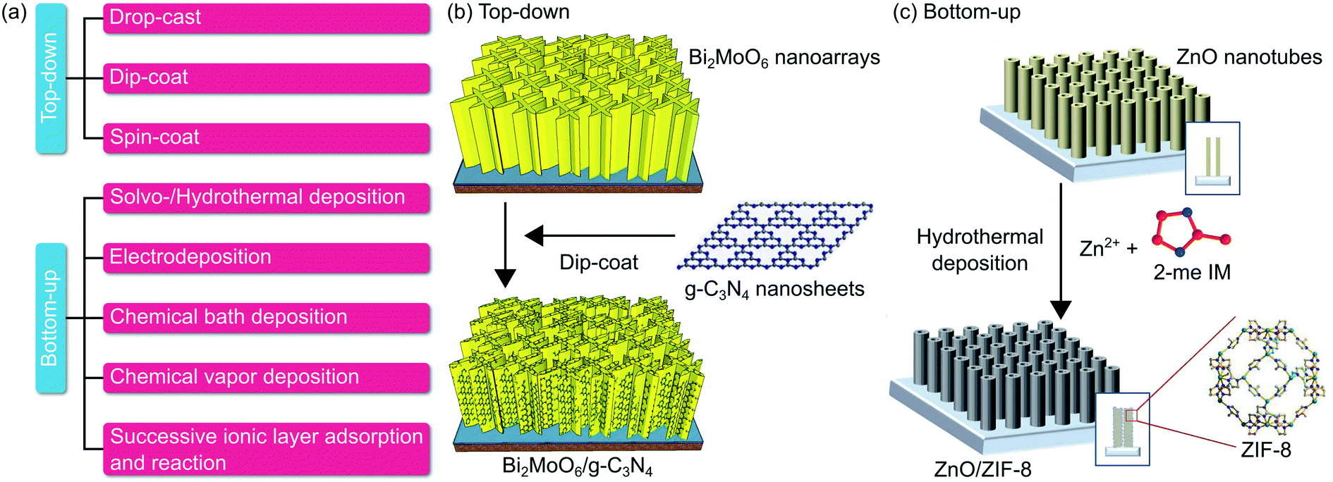 | ||
| Fig. 7 (a) General categorization of MOs/2D materials heterostructure synthesis strategies. (b) Representative top-down route of dip-coat. (c) Representative bottom-up route of hydrothermal. Figures adapted with permission from: (b) ref. 86. Copyright 2016 Elsevier B.V. (c) Ref. 189. Copyright 2019 Wiley-VCH. | ||
On the other hand, the bottom-up route stacks atom-by-atom in form of precursors to build material with desired size and dimension. Typically, 2D materials precursor is placed in a reactor alongside MOs on top of a substrate. Bottom-up method includes solvo-/hydrothermal deposition,189 electrodeposition,170 chemical bath deposition (CBD),167 chemical vapor deposition (CVD),192 and successive ionic layer adsorption and reaction (SILAR).89 The reaction takes place directly on the surface of the MOs to produce MOs/2D materials heterostructure. This route offers low cost and scalability, although it is time-consuming. Fig. 7c depicts the work of Han et al., in which ZnO/ZIF-8 heterostructures were synthesized by placing ZnO nanotubes on FTO substrate face-down along with 2-methylimidazole precursor and methanol medium in a Teflon-lined autoclave at 90 °C for 24 h.189
Metal oxides/Xenes heterostructures
Xenes is a class of elemental monolayer made up of materials in group IVA-VA in the periodic table. Generally, Xenes exhibit high surface areas, high flexibility, good stability during surface reactions, and high tunability of physicochemical properties.207,208 Moreover, the distinctive atomic configuration of each Xenes bestows an adjustable electronic band structure. For instance, group IVA Xenes like graphene, silicene, and germanene possess a semi-metallic characteristic, while VA group Xenes (phosphorene, arsenene, antimonene, and bismuthene) are semiconductors.207 Except for graphene, Xenes do not form the ideal planar hexagonal structure. The large gap between each atom causes Xenes to preferably exist in a buckling structure, rather than a perfect planar hexagonal lattice, with a particular buckling angle and height.208Recently, Tayebi et al. integrated ZnO nanorods with graphene nanosheets, creating a 1D–2D heterostructure with spatial charge separation, as shown in Fig. 8a.180 While ZnO nanorods show a good light absorption within the UV range (that drastically drops in the visible because of a wide Eg of 3.25 eV), graphene exhibits no Eg due to the existence of Dirac cone. Integrating graphene onto ZnO nanorods shifts the Eg to 2.90 eV, i.e., within the visible range. Under 150 mW cm−2 illumination, a photocurrent density of 0.30 mA cm−2 at 1.23 V vs. RHE was demonstrated, nearly three-fold higher than that of bare ZnO (Fig. 8b). Interestingly, the ZnO nanoparticles/graphene sample only yielded 0.20 mA cm−2 at the identical potential due to a fast charge recombination generally found in nanoparticles. They also reported the graphene's ability to mitigate ZnO photocorrosion under UV illumination. Specifically, the addition of graphene significantly reduced the photocorrosion from 27.0% on ZnO to 0.5% on ZnO nanorods/graphene heterostructure. Finally, using impedance spectroscopy (see Fig. 8c for the Nyquist plot), lower charge transfer resistance (Rct) was revealed in ZnO nanorods/graphene heterostructure as compared to that of bare ZnO and ZnO nanoparticles/graphene heterostructure.
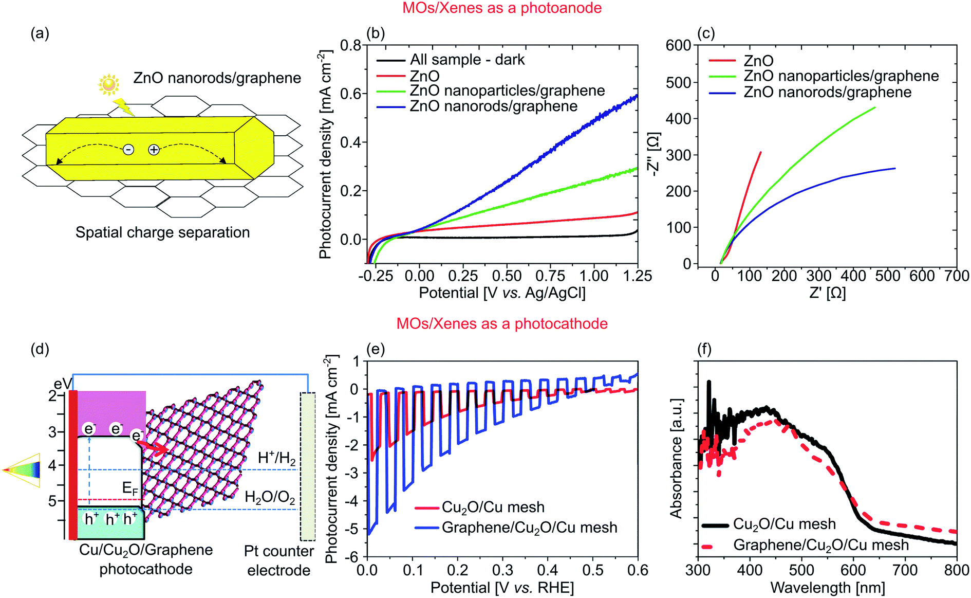 | ||
| Fig. 8 (a) An illustration of enhanced photogenerated charge separation in ZnO nanorods/graphene heterostructure. (b) Photocurrent density of ZnO, ZnO nanoparticles/graphene, and ZnO nanorods/graphene. (c) Nyquist EIS plots of ZnO, ZnO nanoparticles/graphene, and ZnO nanorods/graphene with 0.5 M Na2SO4 as electrolyte. (d) Band alignment of Cu mesh/Cu2O/graphene photocathode. (e) Photocurrent density and (f) UV-visible spectra of Cu mesh/Cu2O/graphene and control Cu mesh/Cu2O samples. Figures adapted with permission from: (a–c) ref. 180. Copyright 2019 Elsevier B.V. (d–f) Ref. 75. Copyright 2014 The Royal Society of Chemistry. | ||
In another work, Zhang et al. reported a composite of BiVO4/black phosphorus as a photoanode for water oxidation.178 In PEC measurements using a 300 W Xe lamp, the heterostructure demonstrated an AM 1.5G photocurrent density of 4.5 mA cm−2 at 1.23 V vs. RHE using KPi as the electrolyte (pH = 7.1). This photocurrent value is fourfold higher than that of BiVO4. Additionally, the addition of black phosphorus nanosheets also improved the stability of BiVO4; ∼99% of the photocurrent was retained over 200 min of chronoamperometry measurement. This enhancement was attributed to the phosphorene layer that provides an exceptional hole transfer channel and minimizes the recombination.
Another approach by Dubale et al., who fabricated a synergetic 1D–2D photocathode of Cu2O/graphene for solar-to-hydrogen production, is depicted in Fig. 8d.75 The addition of graphene onto the Cu2O nanowires drastically improved the AM 1.5G photocurrent density from −2.3 mA cm−2 to −4.8 mA cm−2 (Fig. 8e). However, an excessive amount of graphene was found to reduce the photocurrent due to parasitic absorption. At the highest graphene concentration studied of 3.0 mg mL−1, the light absorption of Cu2O dropped (Fig. 8f), resulting in a photocurrent density of only −1.5 mA cm−2. It is also important to note that the presence of graphene did not alter the absorption edge of the heterostructure, which was 2.03 eV. The best performing sample with 1.0 mg mL−1 of graphene demonstrated a higher visible light absorption and an enhanced photogenerated electrons transfer from the CB of Cu2O to graphene, resulting in lower charge recombination.75 The system also achieved 3.3% of ABPE at −0.6 V vs. Pt and enhanced stability with 83.3% of the photocurrent retained over the course of 20 minutes. Moreover, the ability of the heterostructure in producing hydrogen was demonstrated by the direct measurement of up to 0.02 mmol of hydrogen using a gas chromatograph.
Metal oxides/MXenes heterostructures
Recently, a new class of few-atoms-thick materials has emerged, termed MXenes.209 MXenes can be derived from MAX bulk crystals (M is the transition metal, A is the group A element, and X is carbon and/or nitrogen) by selective etching to remove the A element, leading to the formation of 2D MX phase or MXenes. MXenes have a hexagonal crystal structure, where M layers are located in between X planes.210 Furthermore, MXenes can be divided into two groups based on its structural formula of Mn+1Xn and Mn+1XnTx, where Tx represents functional groups of –OH, –O, or –F.210 As the consequence of the etching process, the formation of those functional groups is unavoidable, thus generating disparate properties from metal to insulator. MXenes therefore exhibit a high versatility in their mechanical, optoelectronic, and transport properties for widespread applications such as photothermal, catalysis, field-effect transistors, and energy storage.210,211One example of MXenes, Ti3C2Tx, has shown a weak thickness dependency in its resistivity, contrary to other 2D materials.212 Ti3C2Tx is obtained by selective etching of Al layers from Ti3AlC2. Fig. 9a shows Ti3C2Tx nanosheets coupled with BiVO4 nanowalls to form a 2D–2D heterostructure photoanode.188 Here, Ti3C2Tx acted as the visible light sensitizer. The heterostructure displayed increased light absorption above 485 nm. However, the Eg remained at around 2.55 eV (Fig. 9b). Due to its energy level, the Ti3C2Tx served as a hole accumulation layer in the heterostructure. Therefore, electrons from BiVO4 were able to flow efficiently to the counter electrode (Pt rod) as the holes were accumulated in Ti3C2Tx, thus extending the lifetime of the charge carriers. Due to this efficient charge separation, the AM 1.5G photocurrent density was improved by >50%, from 2.1 mA cm−2 to 3.5 mA cm−2 (1.23 V vs. RHE). They also reported re-annealing treatment in Ar environment at 300 °C for 30 min (RA-BiVO4) to produce better contact between bare BiVO4 and the conductive substrate, which resulted in a higher photocurrent density of 3.0 mA cm−2. Furthermore, the heterostructure generated 0.8% ABPE at 0.8 V vs. RHE and 56.0% IPCE at 400 nm compared to 0.4% and 29.0% for a bare BiVO4, respectively.188Fig. 9c displays the Mott–Schottky plot of the bare and modified BiVO4, revealing the n-type characteristic of all samples indicated by the positive gradient. The flat-band potential (Vfb) also disclosed a negative onset in reference to the bare BiVO4, and the decreasing slope suggested increasing donor density as compared to the bare BiVO4.
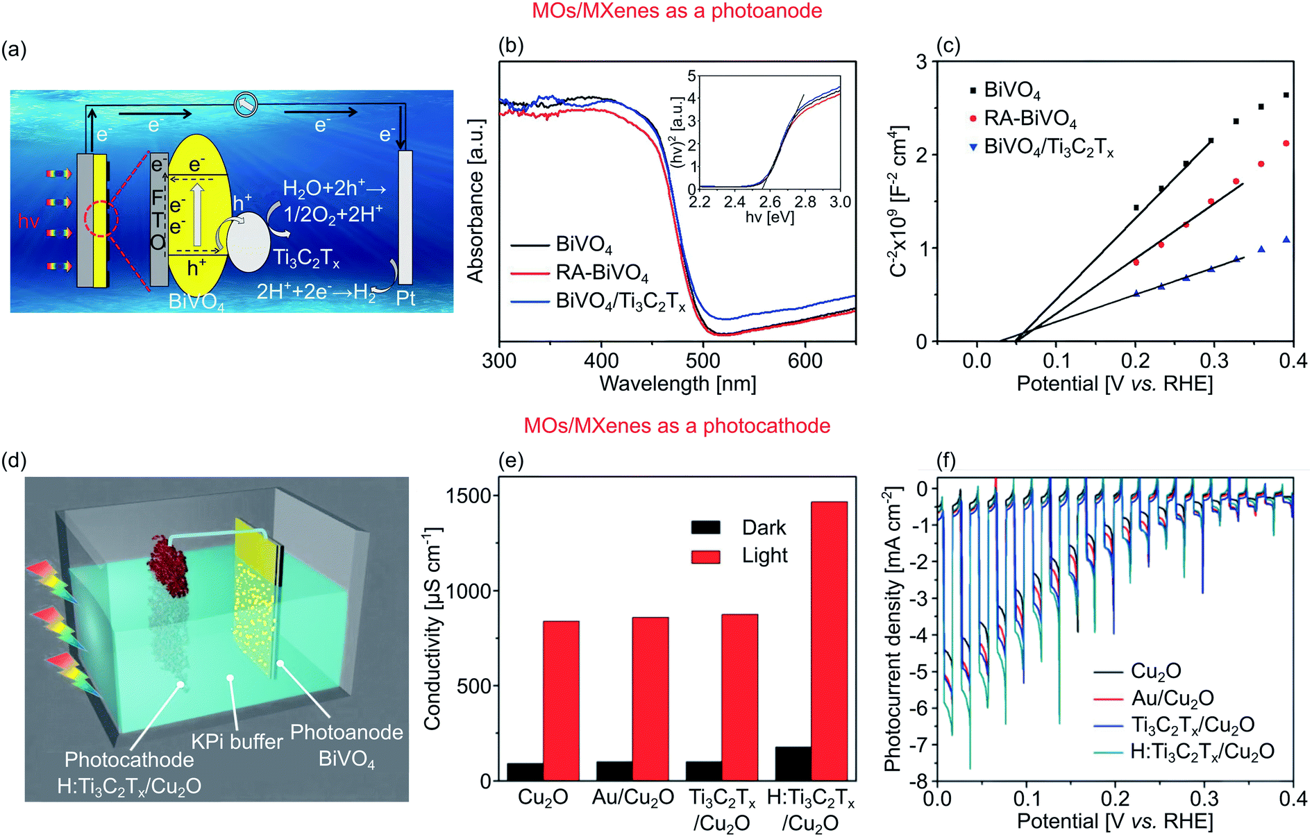 | ||
| Fig. 9 (a) Surface reactions over BiVO4/Ti3C2Tx heterostructure as photoanode. (b) UV-visible absorbance spectra of measured samples. Inset: the corresponding Kubelka–Munk plot. (c) Mott–Schottky plots of all samples showing positive gradient. (d) A schematic of unassisted PEC water splitting devices consisted of Ti3C2Tx/Cu2O as photocathode and BiVO4 as photoanode. (e) Conductivity ratio under dark and light condition over Cu2O, Au/Cu2O, Ti3C2Tx, and Cu2O/H:Ti3C2Tx. (f) J–V curves of the measured samples. Figures adapted with permission from: (a–c) ref. 188. Copyright 2019 Elsevier B.V. (d–f) Ref. 74. Copyright 2014 Elsevier B.V. | ||
As a photocathode, Ti3C2Tx nanosheets also showed promising results when combined with Cu2O nanorods superstructure, creating a 3D–2D heterostructure as represented in Fig. 9d.74 Ti3C2Tx loading on top of Cu2O extended the light absorption; the absorption edge is red-shifted from ∼640 nm (1.93 eV) to ∼680 nm (1.82 eV). Oxygen vacancies were introduced to the nanosheets by performing a H2/Ar post-annealing (H:Ti3C2Tx), resulting in further improvement of light absorption and increased conductivity (from 200 to 1500 μS cm−1, see Fig. 9e).74 Overall, the Cu2O/H:Ti3C2Tx heterostructure exhibited AM 1.5G photocurrent density of −4.5 mA cm−2 at 0 V vs. RHE, which is 10% higher than that of bare Cu2O (Fig. 9f); the ABPE and IPCE were also improved similarly.
Metal oxides/boron carbon nitrides heterostructures
There are several 2D materials in the boron carbon nitride (BCN) family that have shown excellent PEC water splitting performance. To date, this class of materials is categorized based on its elemental composition: boron nitride (BN), boron carbon nitride (BCN) itself, and carbon nitride (C3N4). BN is a 2D layered material where boron and nitrogen atoms are bonded to form a hexagonal lattice. Similar to other 2D materials, multiple layers of B–N planes are stacked together by vdW forces. BN comprises several crystal structures, hexagonal (h-BN), rhombohedral (r-BN), wurtzite (w-BN), cubic (c-BN), and wurtzite (w-BN).213 The hexagonal phase, h-BN, has been reported to be the most stable crystal among them.214 It also exhibits outstanding thermal stability, electrical conductivity, adsorption capacity, and large surface areas.213 However, because of its wide Eg (∼5.0 eV), a stand-alone h-BN cannot be used to efficiently absorb sunlight in PEC water splitting. Hence, h-BN is usually coupled with other semiconductors with lower Eg, e.g., Bi2WO6 (ref. 88) or WO3,82 to expand its light harvesting ability. Alternatively, several researchers synthesized the ternary version of BCN, which possess an intermediate property between insulating h-BN and semi-metallic graphene.215,216 The BCN may exhibit semiconducting properties and its Eg can be engineered via the carbon content in the h-BN lattice.215Another rising material in the BCN family is the polymeric-based material of carbon nitride (C3N4). Because of its ability to absorb visible light (Eg = 2.7 eV), suitable band positions for water reduction and oxidation, high biocompatibility, and low cost, C3N4 is a potential material for PEC water splitting. C3N4 has a number of different structures: alpha (α-C3N4), beta (β-C3N4), graphitic (g-C3N4), cubic (c-C3N4), and pseudo-cubic (pc-C3N4); all with diverse characteristics, in which g-C3N4 is the most thermodynamically stable one.217 To this end, g-C3N4 can be derived from either s-triazine or tri-s-triazine rings.217 Similar to the h-BN counterpart, g-C3N4 has a hexagonal lattice structure with vdW forces holding the layers.
One example where BCN is integrated into a heterostructure for PEC water splitting was demonstrated by Li et al.88 In this work, they integrated one of the Aurivillius MOs of Bi2WO6 quantum dots with h-BN nanosheets to create a 0D–2D heterostructure for water oxidation (Fig. 10a). In its isolated form, Bi2WO6 quantum dots yield a strong UV absorption due to the large Eg of 2.90 eV. The loading of 0.01 M h-BN into Bi2WO6 altered the latter optical properties in that it became sensitive to the visible light, as indicated by the red-shift of the absorption edge to 462 nm (2.68 eV). This widened absorption range also materialized into a higher photocurrent density of 0.9 mA cm−2; 4.5 times higher than that of Bi2WO6 quantum dots (Fig. 10b). The authors argued that the improvements were triggered by the presence of boron vacancies in the h-BN, originating from the thermal substitution method. This defect then led to a negative charge h-BN at approximately −0.25e, compared to pristine h-BN at +0.67e. Due to electrostatic interactions, the negative charge introduced attractive force on the defect site (edge N atoms) toward holes originated from Bi2WO6, thus facilitating hole transfer from Bi2WO6 toward h-BN.88Fig. 10c shows that the smallest diameter of Rct (5.9 kΩ) was demonstrated in 5BN/BW quantum dots (12.6% lower than pristine h-BN), indicating the highest charge transfer across the heterostructures.
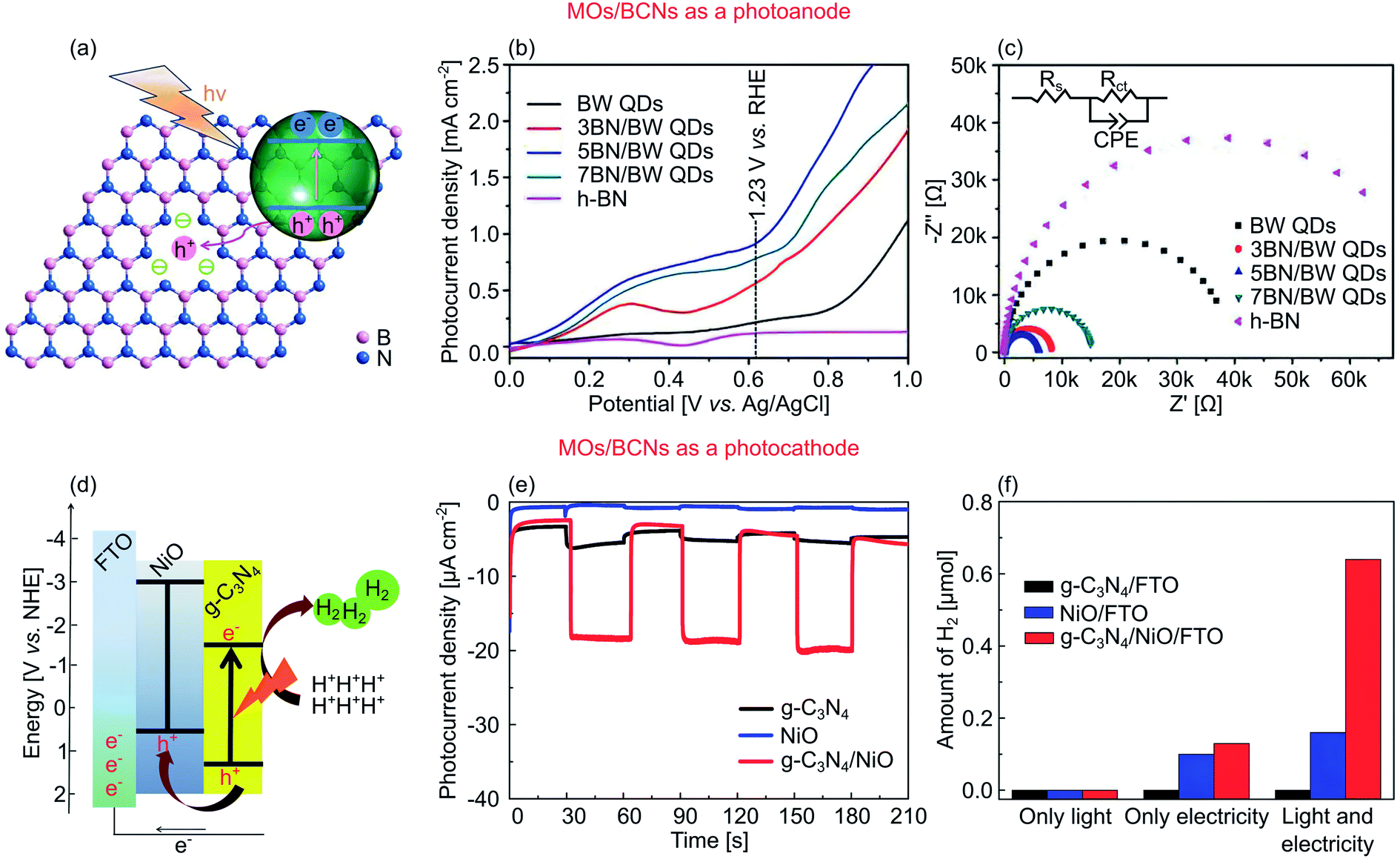 | ||
| Fig. 10 (a) A schematic of synthesized defect-rich h-BN along with the charge transfer mechanism in Bi2WO6 quantum dots (QDs)/h-BN composite. (b) LSV curves and (c) EIS Nyquist plot with the equivalent circuit of Bi2WO6 quantum dots, h-BN, and their composites of 3BN/BW QDs, 5BN/QDs, and 7BN/QDs. The number represents the amount of h-BN loading, i.e., 3 (0.006 M h-BN), 5 (0.01 M h-BN), and 7 (0.014 M h-BN). (d) A hydrogen production illustration based on NiO/g-C3N4 grown on FTO as a photocathode. (e) J–V curves of NiO/g-C3N4 and their component counterparts. (f) Corresponding hydrogen production rate for 4 h in three different conditions: under light (without bias potential), only electricity (−0.2 V vs. RHE), and light and electricity (−0.2 V vs. RHE under visible light illumination). Figures adapted with permission from: (a–c) ref. 88. Copyright 2019 Wiley-VCH. (d–f) Ref. 199. Copyright 2016 The Royal Society of Chemistry. | ||
Furthermore, Arzaee et al. recently have developed a α-Fe2O3/g-C3N4-based photoanode immersed in 0.5 M Na2SO4 (pH = 7).159 The heterostructure exhibited an extended visible light absorption and higher absorption below 470 nm due to the g-C3N4 shell on top of the α-Fe2O3 core. However, a sharp spike in the phototransient curve of α-Fe2O3/g-C3N4 suggests that charge recombination is prevalent in the heterostructure, and an improved interface may be needed to avoid the undesired reaction between electrons and O2 molecules in the electrolyte.
In another work, Dong et al. successfully created a type II hybrid of 3D nanoporous NiO and 2D nanosheets g-C3N4 as a photocathode (Fig. 10d).199 With a Eg of ∼2.85 eV, a bare polymeric g-C3N4 can only absorb light up to 440 nm. By hybridizing this 2D material with a wide Eg semiconductor of NiO, the absorption is extended up to ∼500 nm. As a result, a 20-fold improvement of the cathodic photocurrent (−0.2 mA cm−2 at 0 V vs. RHE) was observed (Fig. 10e). The heterostructure also maintained a steady photocurrent density over 10 h of photostability testing at 0 V vs. RHE. Finally, it exhibited a hydrogen production rate of 0.16 μmol h−1; a four-fold higher rate compared to bare NiO at 0.04 μmol h−1 (−0.2 V vs. RHE under light illumination), as shown in Fig. 10f.
Metal oxides/transition metal dichalcogenides heterostructures
Transition metal dichalcogenides (TMDs) is a class of layered materials with the structure of MX2, where M represents the transition metal such as molybdenum (Mo) or tungsten (W), and X denotes sulphur (S) or selenide (Se). In this arrangement, M atoms are sandwiched by X atoms. TMDs display three phases depending on their stacking order: semiconducting phase of 2H (hexagonal) and 3R (rhombohedral) with trigonal prismatic coordination, and metallic phase of 1T (trigonal) with octahedral coordination.107 Among them, 2H is the most thermodynamically stable phase, while 1T is metastable. In terms of catalytic activity, the 1T phase offers higher activity due to its active basal planes compared to those inert ones in 2H.218 According to their electronic band structures, TMDs has a thickness-dependent Eg. MoS2, the most studied TMDs to date,50,126,219,220 exhibits an indirect Eg of 1.29 eV in the bulk form.107 Because of the confinement effect, monolayer MoS2 has a direct Eg of 1.90 eV.107 WSe2 also shares the same phenomenon with the bulk and monolayer Eg being an indirect 1.20 eV and a direct 1.61 eV, respectively.221 Another class of chalcogenide-based 2D materials is several nanometers-thick CdX (X = S or Se) with buckled hexagonal structure.222,223 CdS and CdSe are visible active semiconductors with Eg of 2.2 and 1.7 eV, respectively. They also exhibit favorable CB and VB positions for both HER and OER, rendering them as promising semiconductors for PEC water splitting.Several authors have reported their efforts in utilizing MOs with TMDs for PEC water splitting. Depicted in Fig. 11a, Li et al. realized a vdW heterostructure of 3D TiO2 nanoflowers and 2D MoSe2 nanosheets with a type II band alignment through a dip-coating process.77 In this case, the amount of MoSe2 in the dipping solution defined the photocurrent density of the heterostructure. Since TiO2 is a wide Eg semiconductor, it is unable to absorb visible light above 400 nm. Complementarily, MoSe2 displays high absorption in the 400–700 nm range. Combining the two, Li et al. showed a heterostructure with smaller Eg of 2.77 eV compared to the bare TiO2 of 2.94 eV.77 They also found that the optimum dipping concentration of MoSe2 is 6 mM, which produced a heterostructure with the lowest photoluminescence signal (Fig. 11b), indicating a low charge recombination rate due to the fast photogenerated electron–hole pairs separation across the heterojunction. Consequently, the same heterostructure also demonstrated the highest AM 1.5G photocurrent density of 0.9 mA cm−2 at 1.23 V vs. RHE (Fig. 11c). Some degree of stability was also demonstrated, as only measurements for up to 400 s were shown; no degradation was detected within this limited period.
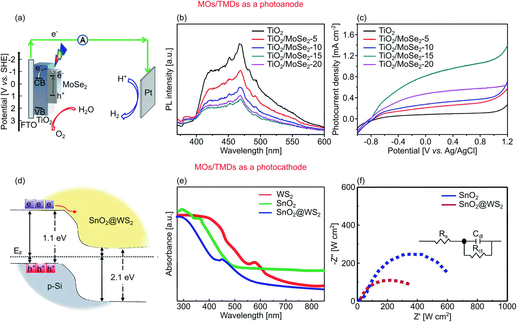 | ||
| Fig. 11 (a) A diagram of PEC water splitting using TiO2/MoSe2 photoanode under visible light. (b) Photoluminescence spectra and (c) polarization curves of TiO2, TiO2/MoSe2-5, TiO2/MoSe2-10, TiO2/MoSe2-15, and TiO2/MoSe2-20. The number represent the amount of MoSe2 loading, 5 (2 mM MoSe2), 10 (4 mM MoSe2), 15 (6 mM MoSe2), and 20 (8 mM MoSe2). (d) Band positions and carrier motion of SnO2/WS2 photocathode to generate hydrogen under visible light. (e) UV-visible absorption and (f) EIS Nyquist plot of SnO2/WS2 photocathode with 0.06 M of WS2 loading, and its constituent controls. Figures adapted with permission from: (a–c) ref. 77. Copyright 2019 Wiley-VCH. (d–f) Ref. 78. Copyright 2019 American Chemical Society. | ||
Another example is by Tekalgne et al., who fabricated a 0D–2D heterostructure of SnO2 nanoparticles/WS2 nanoflowers as a photocathode as illustrated in Fig. 11d.78 The effect of WS2 loading on SnO2 is evident from the optical absorption spectra. The SnO2/WS2 heterostructure underwent a shift in the absorption edge at 565 nm (2.10 eV), as shown in Fig. 11e. The charge separation was also considerably enhanced, which is indeed expected based on the type II band alignment. The study also demonstrated the detrimental effect of excessive co-catalyst loading, where it lowered the photocurrent density due to parasitic absorption in the WS2 layer. WS2 loading of 0.06 M generated −3.5 mA cm−2 at 0 V vs. RHE, while higher WS2 loading (0.08 M) only generated −2.4 mA cm−2.78 Because of the lower charge recombination with the addition of 0.06 M WS2 (Fig. 11f), the heterostructure had lower Rct compared to pure SnO2. Other works by Zheng et al. and Pathak et al. used a similar approach to sensitize TiO2 nanotubes with a novel TMD of PbS quantum dots for water oxidation.163,164 EIS analysis under simulated illumination revealed that the heterostructure of TiO2/PbS had a minuscule Rct in the low frequency range, signifying low charge recombination due to the improved charge separation.
Metal oxides/metal–organic frameworks heterostructures
Metal–organic frameworks (MOFs) are a class of polymer-based materials with high porosity, comprising metal ions as nodes and organic linkers.224 The high porosity feature translates to a massive surface area, with the record experimental value of 7140 m2 g−1.225 Beyond surface area, MOFs also offer other benefits, such as thermal and mechanical stabilities, large pore volumes, excellent host–guest chemistry, and highly adaptable functionalities. As a result, MOFs have been demonstrated for diverse applications such as gas adsorption,226 energy storage,227 solar energy conversion,228 and sensors.229 For PEC water splitting, MOFs with high stability in an aqueous medium can be achieved with either high or low coordination numbers. High valence metals (Zr4+, Fe3+, and Cr3+ with carboxylate bridging units) can establish a rigid structure so that the MOFs interact less with water molecules, thus preventing structural degradation.230 Low valence metals (Zn2+, Co2+, Cu2+, and Ni2+ with azolate linkers), on the other hand, can also form a stable framework in an aqueous medium owing to the formation of a tetrahedral structure that binds to the azolate linkers with angles resembling highly stable zeolite minerals.231Recently, Dou et al. demonstrated the effect of MOFs incorporation for PEC water splitting using low valence metal group as depicted in Fig. 12a.190 They established a ZnO nanorods/cobalt-derived MOF (ZIF-67) photoanode in a core–shell heterostructure system. Pure ZnO displays an absorption edge at around 410 nm, suggesting a large Eg of 3.18 eV. The hybridization with ZIF-67 slightly shifted this edge, hence the Eg. However, according to the UV-visible absorption spectrum, ZIF-67 provided a substantial improvement in light trapping ability for the heterostructure within 450–700 nm due to its porous nature. The effect of porous ZIF-67 was also prominent for the charge transfer efficiency. Here, ZIF-67 improved the transfer of photogenerated electrons by forming multiple transfer channels from the ZIF-67 shell toward the ZnO core, resulting in a lower probability for charge recombination. Fig. 12b shows the resulting ABPE and IPCE of 0.1% (0.2 V vs. SCE) and 3.1% at 400 nm, respectively. ZnO had a low AM 1.5G photocurrent density of 0.4 mA cm−2 due to intensive charge recombination, which was greatly increased to 1.1 mA cm−2 when ZIF-67 was introduced (0.6 V vs. SCE), as shown in Fig. 12c. This was further improved to ∼2.0 mA cm−2 when Au is also introduced due to the plasmonic effect. The heterostructure generated a higher oxygen evolution rate of 30 μmol h−1, nearly three times higher compared to bare ZnO.
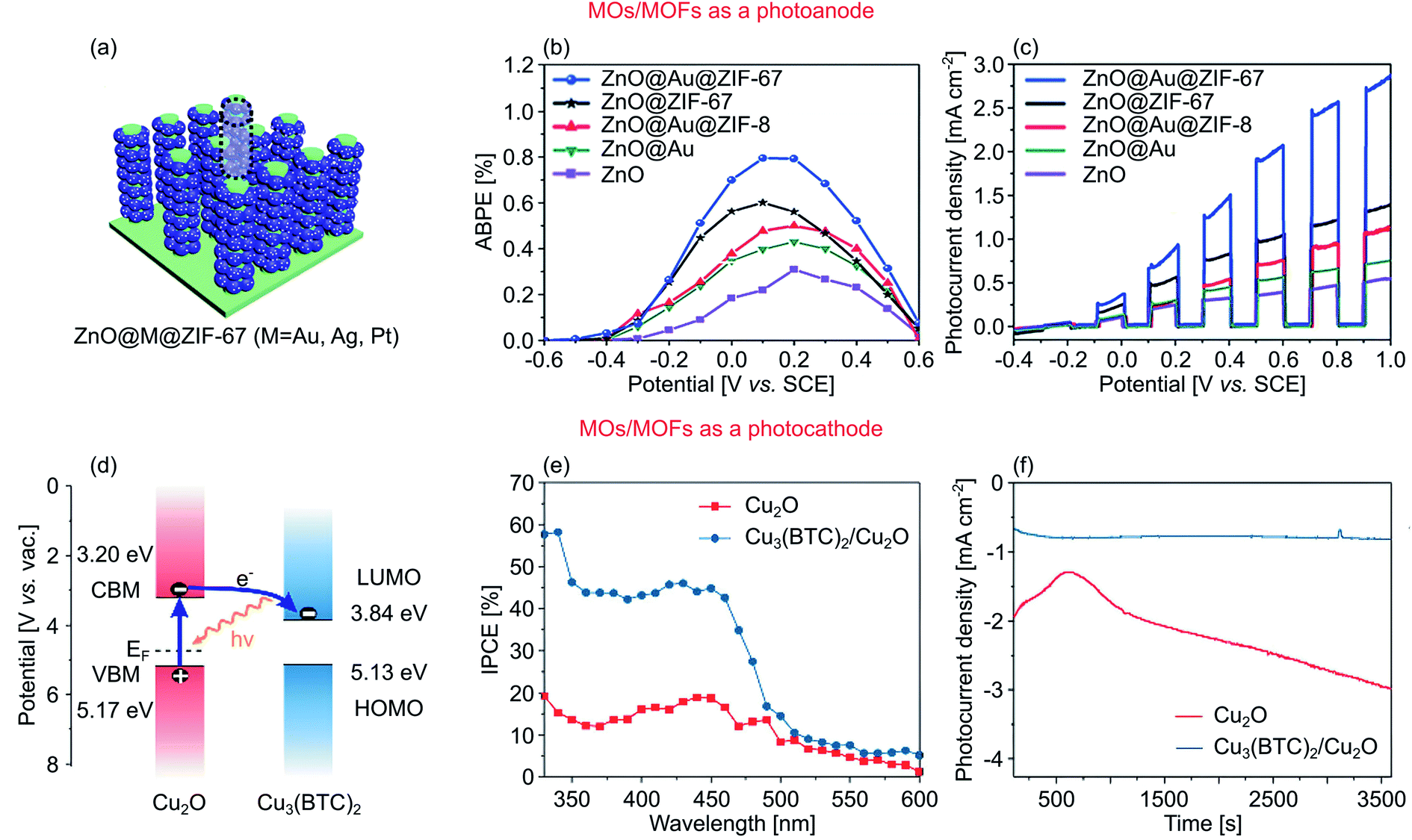 | ||
| Fig. 12 (a) An artist's rendition of ZnO@M@ZIF-67 (M = Au, Ag, Pt) photoanode for PEC water splitting. (b) ABPE as a function of applied potential, and (c) polarization curves of ZnO, ZnO@Au, ZnOZ@ZIF-67, ZnO@Au@ZIF-67, and ZnO@Au@ZIF-8 heterostructures under chopped-light irradiation. (d) Schematic band diagram of Cu2O/Cu3(BTC)2 heterostructure photocathode. (e) Wavelength-dependent IPCE and (f) I–t curves of the Cu2O and Cu2O/Cu3(BTC)2. Figures adapted with permission from: (a–c) ref. 190. Copyright 2017 The Royal Society of Chemistry. (d–f) Ref. 233. Copyright 2019 American Chemical Society. | ||
Other contributions in developing MOs/MOFs heterostructure were also done by Jiao et al. and Cui et al. that utilized MIL-100(Fe) to boost the OER activity of Fe/W co-doped BiVO4 (ref. 232) and TiO2,194 respectively. Both studies reported a mutual finding where the deposition of MIL-100(Fe) provided an efficient charge transfer channel for photogenerated charges and highly active OER sites originated from unsaturated Fe.
Porous MOFs have also been employed as a photocathode as demonstrated by Deng et al., who fabricated a heterostructure of Cu-based MOF of HKUST-1 or Cu3(BTC)2 in conjunction with p-type Cu2O, as illustrated in Fig. 12d.233 The presence of Cu3(BTC)2 on top of Cu2O only had a little impact on the light harvesting ability indicated by the absorption edge. Nevertheless, the porous nature of Cu3(BTC)2 improved the photocurrent density by providing a larger catalytically active area and by forming a preferential electron transfer channel from Cu2O to Cu3(BTC)2, affecting the IPCE as the heterostructure registered 44.0% IPCE at 400 nm, compared to 18.0% of pristine Cu2O under the same condition (Fig. 12e). The J–t curves of the heterostructure displayed a constant photocurrent density of −0.7 mA cm−2 throughout the testing period (3500 s), signifying a great photostability (Fig. 12f).
Metal oxides/bismuth oxyhalides heterostructures
Bismuth oxyhalides are semiconducting layered materials with the ternary composition of BiOX, where X is the halide element of Cl, Br, or I. They have a tetragonal matlockite crystal structure with each layer comprising an oxygen plane in between two halide and bismuth planes with the covalent arrangement of X–Bi–O–Bi–X. Typically, BiOX shows exceptional physicochemical properties and has been investigated for several applications, such as reflective pigments,234 water purification,235 gas sensors,236 storage materials,237 and catalysis.238 In PEC water splitting, it has been identified that BiOX has an increased photogenerated charge separation in the [001] direction due to the perpendicular electric field within a single layer of BiOX.198,239 Additionally, it has been argued that their indirect Eg is beneficial for PEC water splitting as the photoexcited electrons need to move through the definite k-space and it considerably lowers the direct charge recombination rate.240Efforts in integrating BiOX with other MO semiconductors also recently received considerable attention. Fig. 13a depicts the work of Ye et al. who reported the combination of ternary MOs of n-type BiVO4 nanoporous with p-type BiOI nanosheets to create a p–n junction photoanode for PEC water splitting.66 Due to the corresponding Fermi level of each semiconductor, electrons in n-type BiVO4 diffused into p-type BiOI, resulting in a positively charged BiVO4, and vice versa. This further enhanced the charge carrier separation and reduced the charge recombination. Such a 2D–2D heterostructure of BiVO4/BiOI could reach 3.3 mA cm−2 AM 1.5G photocurrent density at 1.23 V vs. RHE, far higher compared to the pristine BiVO4 at 1.2 mA cm−2 under identical circumstances. Furthermore, the ABPE reached as high as 1.0% at 0.7 V vs. RHE. Correspondingly, the heterostructure's IPCE also showed an improvement about three times higher of 44.0% at 400 nm compared to the pure BiVO4 (Fig. 13b). The separation efficiency was also studied using 15% H2O2 as hole scavenger alongside 0.5 M KH2PO4 electrolyte to eliminate any catalytic limitation or surface recombination. Under an applied potential of 1.23 V vs. RHE, the heterostructure's separation efficiency reached ∼70%, which is more than double that of BiVO4 at ∼30%, signifying suppressed charge recombination originated from the presence of a p–n junction (Fig. 13c).
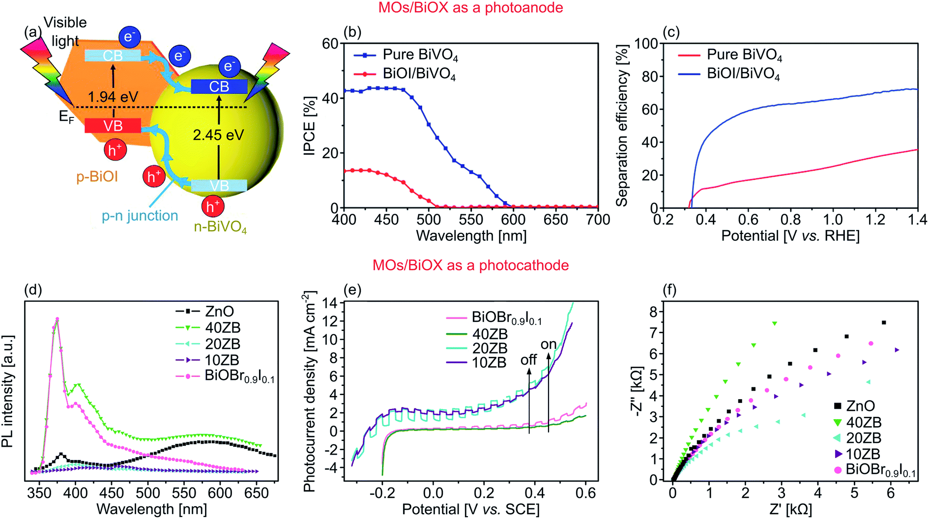 | ||
| Fig. 13 (a) Photogenerated charge movement and band alignment of BiVO4/BiOI photoanode. (b) IPCE spectra of BiVO4 and BiOI/BiVO4 at given wavelength at 0.68 V vs. RHE using 0.5 M KH2PO4 as the electrolyte. (c) Surface charge transfer efficiency using 15% H2O2 as a hole scavenger. (d) Photoluminescence spectra. (e) J–V curves under chopped visible light of, and (f) EIS Nyquist plot of ZnO/BiOBr0.9I0.1 (ZB) heterostructures as a photocathode, alongside control ZnO and BiOBr0.9I0.1. Numbers 10, 20, and 40 denote ZnO wt%. Figures adapted with permission from: (a–c) ref. 66. Copyright 2015 Elsevier B.V. (d–f) Ref. 198. Copyright 2020 Elsevier B.V. | ||
Several groups also reported other integration of MOs and BiOX. For example, Zhou et al. fabricated TiO2/BiOCl,177 while Zhou et al. synthesized CuWO4/BiOI89 to create a p–n junction heterostructures for OER. The creation of p–n junction in both cases significantly lowered the probability of carriers to recombine by providing an efficient built-in electric field induced by the depletion region on the surface of the heterostructures.
As a photocathode, BiOX of 2D non-stoichiometric BiOBr0.9I0.1 nanoflakes has also been coupled with 2D ZnO nanosheets that have reversible conductivity type modulation from n-type to p-type, or vice versa, based on the ZnO's mass fraction.198 The radiative recombination could be determined by PL spectra, where the increased emissions at 374 nm (near-band-edge), along with 400 and 581 nm (defects) from 40ZB sample (i.e., 40 wt% ZnO) compared to pure ZnO counterpart can be attributed to intensified radiative recombination. However, 10ZB and 20ZB samples register lower PL emissions, suggesting an improved charge separation (Fig. 13d). According to the reflectance spectra, the pristine ZnO and BiOBr0.9I0.1 showed an absorption edge at 412 and 537 nm, revealing their Eg of 3.00 and 2.42 eV, respectively. In their heterostructure form, a negligible Eg shift was detected. However, the heterostructure showed an increased light absorption within the visible range as a function of the wt% of ZnO. Moreover, increasing the wt% of ZnO modified the nature of the conductivity from n- to p-type. The pristine BiOBr0.9I0.1 exhibited an anodic photocurrent density, signifying an n-type conductivity. When the ZnO content reaches 10 wt%, the heterostructure showed a cathodic photocurrent instead, suggesting a switch to a p-type conductivity (Fig. 13e). This conductivity tuning was attributed to the presence of defects along the interfaces. At this stage, i.e., when the ZnO content is still not that high, Zn2+ substituted Bi3+ without forming sufficient oxygen vacancies. As a consequence, additional holes were introduced as the charge compensation, altering the properties of BiOBr0.9I0.1 from n-type to p-type.198 Increasing the mass fraction of ZnO further to 40 wt%, however, also introduced more oxygen vacancies, which is often suggested as electron donors. Therefore, these excessive donors reverted the conductivity type to n-type. Under chopped visible light, the heterostructure with 20 wt% of ZnO registered a cathodic photocurrent density of 0.8 μA cm−2 at −0.2 V vs. SCE. This reversible conductivity type also affected the carrier mobility shown by the Nyquist plot with smaller Rct, where the p-type ZnO/BiOBr0.9I0.1 (20ZB) was more efficient in suppressing the charge recombination than the n-type counterpart (40ZB) (Fig. 13f).
Conclusion and outlook
In summary, we have thoroughly reviewed the various nanoscale heterostructures that are composed of metal oxides and 2D materials. This exercise is motivated by the many limitations of metal oxides as one of the most investigated materials for PEC water splitting. In particular, many metal oxide photoelectrodes suffer from having a narrow visible light absorption, unfavorable band position, and poor charge carrier mobilities. Some oxides also suffer from instability in aqueous solutions due to self-oxidation or reduction. The formation of nanoscale heterostructure with 2D materials simultaneously addresses these limitations. From the literature, it is clear that the efforts in developing MOs/2D materials heterostructure as photoanodes are more prominent than as photocathodes. This finding is in mutual agreement with the research direction in PEC water splitting, where OER poses more challenges compared to HER (e.g., sluggish OER kinetics). Correspondingly, the building block of photoanodes is an n-type semiconductor, which is fulfilled by most MOs (e.g., ZnO, TiO2, α-Fe2O3, and BiVO4) due to the low formation energy of electron donor defects, such as oxygen vacancies.241 On the other hand, photocathodes require p-type semiconductor, which is a much less reported for MOs (a couple of examples include NiO and Cu2O) because of the high energy barrier of hole acceptor defects (i.e., cation vacancies) and low formation energy of hole nullifier defects (i.e., anion vacancies).241 We also surveyed and categorized the heterostructures based on the nanoscale dimensionality (i.e., 0D, 1D, 2D, 3D). In most cases, MOs are morphed into a 1D morphology (e.g., nanorods, nanowires, and nanotubes) to capitalize on their high surface areas for light trapping and catalysis owing to their high aspect ratio (length vs. diameter). On the other hand, 2D materials have also been employed in their lower dimensionality forms of 0D (quantum dots) or 1D (nanotubes; by folding the 2D plane into a cylindrical shape, similar to the case of carbon nanotubes). For the most part, 2D materials are interfaced as is, to fully take the advantage of the abundant basal planes of the 2D plane that can be engineered into active sites for catalysis. We also reviewed the possible interfacial electronic structure alignment in the heterostructures (i.e., type II, p–n junction, and Z-scheme). We found that type II is more frequently compared to other mechanisms due to its simplicity (assuming that the energy levels from the two materials allow charge transfer). Z-scheme, on the other hand, is a less established system, but shows notable architecture developments in charge transfer channels (i.e., traditional shuttle redox mediator, all-solid-state, and direct Z-scheme).143 Thus, in our perspectives, deeper exploration in Z-scheme MOs/2D materials heterostructure is to be expected in the future.The combination of metal oxides with specific material classes within the various 2D materials family is also highlighted. In many of these cases, the introduction of 2D materials successfully (i) increases the visible light absorption range, (ii) enhances the charge carrier separation due to the formation of a favorable interface, (iii) induces manifold improvement of the photocurrent, and (iv) extends the stability of the metal oxide photoelectrodes. Among these reports, graphene and its derivatives (e.g., graphene oxide and reduced graphene oxide) still dominate as the most commonly used 2D materials in PEC water splitting, but growing numbers of work are available that employ more abundant and simpler-to-synthesize 2D materials, e.g., transition metal dichalcogenides and boron carbon nitride. Fig. 14 visualizes the performance (in terms of the reported photocurrent densities at the water redox potentials) of these vast combinations of MOs/2D materials heterostructures over the last decade (see the complete list in Tables 1 and 2).
 | ||
| Fig. 14 Achieved photocurrent densities (Jph) at standardized potentials of 1.23 V vs. RHE for OER (top) and 0 V vs. RHE for HER (bottom) for various MOs/2D materials heterostructures over the last decade. | ||
Despite the progress and growing amount of interest, it is clear that the development of MOs/2D materials heterostructures for PEC water splitting is still some steps away from the required target. Photoelectrodes that deliver high performance (e.g., photocurrent density >5 mA cm−2) have been reported over the past decade, but the number is limited, and they represent more the exception rather than the norm. This is of course disappointing given the premise of various advantages from adopting such a heterostructure for PEC water splitting. Such a limitation, however, does not seem to be specific to the heterostructure architecture itself; instead, the limited performance seems to be caused by the intrinsic limitations of the investigated MOs so far. In addition, efforts in the field in coupling the appropriate MOs and 2D materials are still mostly based on trial and error, instead of driven by guidelines. It is therefore clear that deeper fundamental studies are still needed to fully unravel and exploit the expected theoretical advantages of such heterostructures. The interface between the two materials is obviously a critical element; we have to first understand the key parameters that define the interfacial properties between the metal oxides and the 2D materials. The combination of advanced spectroscopic experiments with material computations will most likely be needed. At the same time, synthesis approaches and fabrication methodologies that allow full control of the interfacial properties will also be needed. From the materials perspective, exploration of novel MOs and 2D materials with appropriate crystal structure and optoelectronic properties aided by advanced calculation methods, e.g., density functional theory (DFT) calculations, accompanied by machine learning may hold the key for future advancement.242 For example, recent advances make it possible to directly synthesize 2D MOs using scalable methods, such as exfoliation by weakening the strong covalent bond of MOs243 and self-assembly by introducing amphiphilic block copolymer and alcohol co-surfactant.244 Therefore, the establishment of heterostructure of these 2D MOs with other 2D materials, specifically for PEC water splitting, is not far from realization. Finally, more general beyond the MOs/2D materials heterostructure, employing principles from other interdisciplinary research may provide novel approaches to accomplish more efficient PEC water splitting devices, such as utilizing solid oxide electrolyte,245 decoupling light absorption and catalysis,51,246 and also hybridizing with plasmon247 or piezotronics.248
Author contributions
A. R. F.: conceptualization, writing – original draft, visualization. F. A. A. N.: conceptualization, writing – review & editing, supervision. F. F. A.: conceptualization, writing – review & editing, supervision. V. F.: conceptualization, writing – review & editing, supervision, funding acquisition.Conflicts of interest
The authors declare no conflicts of interest.Acknowledgements
A. R. F. and V. F. acknowledge support from the Direktorat Riset dan Pengembangan Universitas Indonesia under the World Class University Funding No. NKB-500/UN2.RST/HKP.05.00/2021. F. A. A. N. acknowledges support from the European Union's Horizon 2020 Research and Innovation Programme under the Marie Skłodowska-Curie Grant Agreement No. 101028262.References
- A. M. M. I. Qureshy, M. Ahmed and I. Dincer, Performance assessment study of photo-electro-chemical water-splitting reactor designs for hydrogen production, Int. J. Hydrogen Energy, 2019, 44, 9237–9247, DOI:10.1016/j.ijhydene.2019.01.280.
- A. du Plessis, Climate Change: Current Drivers, Observations and Impacts on the Globe's Natural and Human Systems, in Water as an Inescapable Risk, Springer International Publishing, Cham, 2019, pp. 27–53, DOI:10.1007/978-3-030-03186-2_3.
- M. E. Mann, S. Rahmstorf, K. Kornhuber, B. A. Steinman, S. K. Miller and D. Coumou, Influence of Anthropogenic Climate Change on Planetary Wave Resonance and Extreme Weather Events, Sci. Rep., 2017, 7, 45242, DOI:10.1038/srep45242.
- B. Neumann, A. T. Vafeidis, J. Zimmermann and R. J. Nicholls, Future coastal population growth and exposure to sea-level rise and coastal flooding – a global assessment, PLoS One, 2015, 10, e0118571, DOI:10.1371/journal.pone.0118571.
- Y. Yang, H. Guan, O. Batelaan, T. R. McVicar, D. Long, S. Piao, W. Liang, B. Liu, Z. Jin and C. T. Simmons, Contrasting responses of water use efficiency to drought across global terrestrial ecosystems, Sci. Rep., 2016, 6, 1–8, DOI:10.1038/srep23284.
- M. D. Hurteau, S. Liang, A. L. R. Westerling and C. Wiedinmyer, Vegetation-fire feedback reduces projected area burned under climate change, Sci. Rep., 2019, 9, 1–6, DOI:10.1038/s41598-019-39284-1.
- M. Wang, A. Elgowainy, U. Lee, A. Bafana, P. Benavides, A. Burnham, H. Cai, Q. Dai, U. Gracida, T. Hawkins, P. Jaquez, J. Kelly, H. Kwon, X. Liu, Z. Lu, L. Ou, P. Sun, O. Winjobi, H. Xu, E. Yoo, G. Zaimes and G. Zang, Greenhouse Gases, Regulated Emissions, and Energy Use in Technologies Model® (2020 Excel), 2020, DOI:10.11578/GREET-Excel-2020/dc.20200912.1.
- S. Shiva Kumar and V. Himabindu, Hydrogen production by PEM water electrolysis – a review, Mater. Sci. Energy Technol., 2019, 2, 442–454, DOI:10.1016/j.mset.2019.03.002.
- F. Sun, J. Qin, Z. Wang, M. Yu, X. Wu, X. Sun and J. Qiu, Energy-saving hydrogen production by chlorine-free hybrid seawater splitting coupling hydrazine degradation, Nat. Commun., 2021, 12, 1–11, DOI:10.1038/s41467-021-24529-3.
- P. Castillo-Moreno, J. C. Serrato, J. C. Willison and J. P. Magnin, Photohydrogen production from lactose and lactate by recombinant strains of Rhodobacter capsulatus: modeling and optimization, Int. J. Hydrogen Energy, 2018, 43, 21231–21245, DOI:10.1016/j.ijhydene.2018.09.038.
- M. Renaudie, V. Clion, C. Dumas, S. Vuilleumier and B. Ernst, Intensification and optimization of continuous hydrogen production by dark fermentation in a new design liquid/gas hollow fiber membrane bioreactor, Chem. Eng. J., 2021, 416, 129068, DOI:10.1016/j.cej.2021.129068.
- T. Geißler, M. Plevan, A. Abánades, A. Heinzel, K. Mehravaran, R. K. Rathnam, C. Rubbia, D. Salmieri, L. Stoppel, S. Stückrad, A. Weisenburger, H. Wenninger and T. Wetzel, Experimental investigation and thermo-chemical modeling of methane pyrolysis in a liquid metal bubble column reactor with a packed bed, Int. J. Hydrogen Energy, 2015, 40, 14134–14146, DOI:10.1016/j.ijhydene.2015.08.102.
- J. H. Kim, H. Kaneko, T. Minegishi, J. Kubota, K. Domen and J. S. Lee, Overall Photoelectrochemical Water Splitting using Tandem Cell under Simulated Sunlight, ChemSusChem, 2016, 9, 61–66, DOI:10.1002/cssc.201501401.
- J. H. Kim, J. W. Jang, Y. H. Jo, F. F. Abdi, Y. H. Lee, R. Van De Krol and J. S. Lee, Hetero-type dual photoanodes for unbiased solar water splitting with extended light harvesting, Nat. Commun., 2016, 7, 1–9, DOI:10.1038/ncomms13380.
- J. Li and N. Wu, Semiconductor-based photocatalysts and photoelectrochemical cells for solar fuel generation: a review, Catal. Sci. Technol., 2015, 5, 1360–1384, 10.1039/C4CY00974F.
- C. Jiang, S. J. A. Moniz, A. Wang, T. Zhang and J. Tang, Photoelectrochemical devices for solar water splitting-materials and challenges, Chem. Soc. Rev., 2017, 46, 4645–4660, 10.1039/c6cs00306k.
- S. J. A. Moniz, S. A. Shevlin, D. J. Martin, Z. X. Guo and J. Tang, Visible-light driven heterojunction photocatalysts for water splitting-a critical review, Energy Environ. Sci., 2015, 8, 731–759, 10.1039/c4ee03271c.
- R. Perez and M. Perez, A Fundamental Look at Supply Side Energy Reserves for the Planet, 2015, https://www.iea-shc.org/data/sites/1/publications/2015-11-A-Fundamental-Look-at-Supply-Side-Energy-Reserves-for-the-Planet.pdf Search PubMed.
- Statistical Review of World Energy 2021, 2021, https://www.bp.com/content/dam/bp/business-sites/en/global/corporate/pdfs/energy-economics/statistical-review/bp-stats-review-2021-full-report.pdf Search PubMed.
- D. Commandeur, G. Brown, E. Hills, J. Spencer and Q. Chen, Defect-Rich ZnO Nanorod Arrays for Efficient Solar Water Splitting, ACS Appl. Nano Mater., 2019, 2, 1570–1578, DOI:10.1021/acsanm.9b00047.
- M. Lamers, W. Li, M. Favaro, D. E. Starr, D. Friedrich, S. Lardhi, L. Cavallo, M. Harb, R. Van De Krol, L. H. Wong and F. F. Abdi, Enhanced Carrier Transport and Bandgap Reduction in Sulfur-Modified BiVO4 Photoanodes, Chem. Mater., 2018, 30, 8630–8638, DOI:10.1021/acs.chemmater.8b03859.
- Z. Ma, O. Linnenberg, A. Rokicinska, P. Kustrowski and A. Slabon, Augmenting the photocurrent of CuWO4 photoanodes by heat treatment in the nitrogen atmosphere, J. Phys. Chem. C, 2018, 122, 19281–19288, DOI:10.1021/acs.jpcc.8b02828.
- J. Brillet, J. H. Yum, M. Cornuz, T. Hisatomi, R. Solarska, J. Augustynski, M. Graetzel and K. Sivula, Highly efficient water splitting by a dual-absorber tandem cell, Nat. Photonics, 2012, 6, 824–828, DOI:10.1038/nphoton.2012.265.
- W. H. Cheng, M. H. Richter, M. M. May, J. Ohlmann, D. Lackner, F. Dimroth, T. Hannappel, H. A. Atwater and H. J. Lewerenz, Monolithic Photoelectrochemical Device for Direct Water Splitting with 19% Efficiency, ACS Energy Lett., 2018, 3, 1795–1800, DOI:10.1021/acsenergylett.8b00920.
- P. Varadhan, H. C. Fu, Y. C. Kao, R. H. Horng and J. H. He, An efficient and stable photoelectrochemical system with 9% solar-to-hydrogen conversion efficiency via InGaP/GaAs double junction, Nat. Commun., 2019, 10, 1–9, DOI:10.1038/s41467-019-12977-x.
- L. Steier and S. Holliday, A bright outlook on organic photoelectrochemical cells for water splitting, J. Mater. Chem. A, 2018, 6, 21809–21826, 10.1039/C8TA07036A.
- F. F. Abdi and S. P. Berglund, Recent developments in complex metal oxide photoelectrodes, J. Phys. D: Appl. Phys., 2017, 50, 193002, DOI:10.1088/1361-6463/aa6738.
- T. J. Brown, N. E. Idoine, E. R. Wrighton, E. R. Raycraft, S. F. Hobbs, R. A. Shaw, P. Everett, C. Kresse, E. A. Deady and T. Bide, World Mineral Production 2014–2018, 2020, https://www.bgs.ac.uk/downloads/start.cfm?id=3512 Search PubMed.
- S. Sun, X. Zhang, J. Cui, Q. Yang and S. Liang, High-index faceted metal oxide micro-/nanostructures: a review on their characterization, synthesis and applications, Nanoscale, 2019, 11, 15739–15762, 10.1039/c9nr05107d.
- Y. Wang, H. Arandiyan, J. Scott, A. Bagheri, H. Dai and R. Amal, Recent advances in ordered meso/macroporous metal oxides for heterogeneous catalysis: a review, J. Mater. Chem. A, 2017, 5, 8825–8846, 10.1039/c6ta10896b.
- V. Esposito and I. E. Castelli, Metastability at Defective Metal Oxide Interfaces and Nanoconfined Structures, Adv. Mater. Interfaces, 2020, 7, 1–22, DOI:10.1002/admi.201902090.
- X. Sun, Q. Li, J. Jiang and Y. Mao, Morphology-tunable synthesis of ZnO nanoforest and its photoelectrochemical performance, Nanoscale, 2014, 6, 8769–8780, 10.1039/c4nr01146e.
- K. R. Tolod, S. Hernández, M. Castellino, F. A. Deorsola, E. Davarpanah and N. Russo, Optimization of BiVO4 photoelectrodes made by electrodeposition for sun-driven water oxidation, Int. J. Hydrogen Energy, 2020, 45, 605–618, DOI:10.1016/j.ijhydene.2019.10.236.
- B. K. Ozcelik and C. Ergun, Synthesis and characterization of iron oxide particles using spray pyrolysis technique, Ceram. Int., 2015, 41, 1994–2005, DOI:10.1016/j.ceramint.2014.09.103.
- C. R. Lhermitte, J. Garret Verwer and B. M. Bartlett, Improving the stability and selectivity for the oxygen-evolution reaction on semiconducting WO3 photoelectrodes with a solid-state FeOOH catalyst, J. Mater. Chem. A, 2016, 4, 2960–2968, 10.1039/c5ta04747a.
- C. Chen, Y. Cheng, Q. Dai and H. Song, Radio Frequency Magnetron Sputtering Deposition of TiO2 Thin Films and Their Perovskite Solar Cell Applications, Sci. Rep., 2015, 5, 1–12, DOI:10.1038/srep17684.
- R. Müller, F. Hernandez-Ramirez, H. Shen, H. Du, W. Mader and S. Mathur, Influence of precursor chemistry on morphology and composition of CVD-grown SnO2 nanowires, Chem. Mater., 2012, 24, 4028–4035, DOI:10.1021/cm300913h.
- A. J. E. Rettie, S. Mozaffari, M. D. McDaniel, K. N. Pearson, J. G. Ekerdt, J. T. Markert and C. B. Mullins, Pulsed laser deposition of epitaxial and polycrystalline bismuth vanadate thin films, J. Phys. Chem. C, 2014, 118, 26543–26550, DOI:10.1021/jp5082824.
- Y. Gao, O. Zandi and T. W. Hamann, Atomic layer stack deposition-annealing synthesis of CuWO4, J. Mater. Chem. A, 2016, 4, 2826–2830, 10.1039/c5ta06899a.
- M. Opel, S. Geprägs, M. Althammer, T. Brenninger and R. Gross, Laser molecular beam epitaxy of ZnO thin films and heterostructures, J. Phys. D: Appl. Phys., 2014, 47, 034002, DOI:10.1088/0022-3727/47/3/034002.
- M. T. M. Koper, Photoelectrochemical Hydrogen Production, Springer US, Boston, MA, 2012, DOI:10.1007/978-1-4614-1380-6.
- X. L. Li, W. P. Han, J. Bin Wu, X. F. Qiao, J. Zhang and P. H. Tan, Layer-Number Dependent Optical Properties of 2D Materials and Their Application for Thickness Determination, Adv. Funct. Mater., 2017, 27, 1604468, DOI:10.1002/adfm.201604468.
- A. Chaves, J. G. Azadani, H. Alsalman, D. R. da Costa, R. Frisenda, A. J. Chaves, S. H. Song, Y. D. Kim, D. He, J. Zhou, A. Castellanos-Gomez, F. M. Peeters, Z. Liu, C. L. Hinkle, S. H. Oh, P. D. Ye, S. J. Koester, Y. H. Lee, P. Avouris, X. Wang and T. Low, Bandgap engineering of two-dimensional semiconductor materials, npj 2D Mater. Appl., 2020, 4, 29, DOI:10.1038/s41699-020-00162-4.
- X. Cai, Y. Luo, B. Liu and H.-M. Cheng, Preparation of 2D material dispersions and their applications, Chem. Soc. Rev., 2018, 47, 6224–6266, 10.1039/C8CS00254A.
- L. Banszerus, M. Schmitz, S. Engels, J. Dauber, M. Oellers, F. Haupt, K. Watanabe, T. Taniguchi, B. Beschoten and C. Stampfer, Ultrahigh-mobility graphene devices from chemical vapor deposition on reusable copper, Sci. Adv., 2015, 1, 1–7, DOI:10.1126/sciadv.1500222.
- N. Gillgren, D. Wickramaratne, Y. Shi, T. Espiritu, J. Yang, J. Hu, J. Wei, X. Liu, Z. Mao, K. Watanabe, T. Taniguchi, M. Bockrath, Y. Barlas, R. K. Lake and C. N. Lau, Gate tunable quantum oscillations in air-stable and high mobility few-layer phosphorene heterostructures, 2D Mater., 2015, 2, 1–8, DOI:10.1088/2053-1583/2/1/011001.
- D. L. Ferreira, J. C. L. Sousa, R. N. Maronesi, J. Bettini, M. A. Schiavon, A. V. N. C. Teixeira and A. G. Silva, Size-dependent bandgap and particle size distribution of colloidal semiconductor nanocrystals, J. Chem. Phys., 2017, 147, 154102, DOI:10.1063/1.4999093.
- K. Dolui and S. Y. Quek, Quantum-confinement and Structural Anisotropy result in Electrically-Tunable Dirac Cone in Few-layer Black Phosphorous, Sci. Rep., 2015, 5, 1–12, DOI:10.1038/srep11699.
- F. E. Osterloh, Inorganic nanostructures for photoelectrochemical and photocatalytic water splitting, Chem. Soc. Rev., 2013, 42, 2294–2320, 10.1039/c2cs35266d.
- C. K. Sumesh and S. C. Peter, Two-dimensional semiconductor transition metal based chalcogenide based heterostructures for water splitting applications, Dalton Trans., 2019, 48, 12772–12802, 10.1039/c9dt01581g.
- M. Ahmed and I. Dincer, A review on photoelectrochemical hydrogen production systems: challenges and future directions, Int. J. Hydrogen Energy, 2019, 44, 2474–2507, DOI:10.1016/j.ijhydene.2018.12.037.
- S. Chen, D. Huang, P. Xu, W. Xue, L. Lei, M. Cheng, R. Wang, X. Liu and R. Deng, Semiconductor-based Photocatalysts for Photocatalytic and Photoelectrochemical Water Splitting: Will We Stop with Photocorrosion?, Royal Society of Chemistry, 2020, 10.1039/c9ta12799b.
- Z. Liu, Q. Cai, C. Ma, J. Zhang and J. Liu, Photoelectrochemical properties and growth mechanism of varied ZnO nanostructures, New J. Chem., 2017, 41, 7947–7952, 10.1039/c7nj01725a.
- P. A. Kempler, R. H. Coridan, N. S. Lewis and N. S. Lewis, Effects of bubbles on the electrochemical behavior of hydrogen-evolving Si microwire arrays oriented against gravity, Energy Environ. Sci., 2020, 13, 1808–1817, 10.1039/d0ee00356e.
- F. Li, D. Zhang, R. C. Xu, W. F. Fu and X. J. Lv, Superhydrophilic Heteroporous MoS2/Ni3S2 for Highly Efficient Electrocatalytic Overall Water Splitting, ACS Appl. Energy Mater., 2018, 1, 3929–3936, DOI:10.1021/acsaem.8b00665.
- X. Shan, J. Liu, H. Mu, Y. Xiao, B. Mei, W. Liu, G. Lin, Z. Jiang, L. Wen and L. Jiang, An Engineered Superhydrophilic/Superaerophobic Electrocatalyst Composed of the Supported CoMoSx Chalcogel for Overall Water Splitting, Angew. Chem., Int. Ed., 2020, 59, 1659–1665, DOI:10.1002/anie.201911617.
- S. Kahng, H. Yoo and J. H. Kim, Recent advances in earth-abundant photocatalyst materials for solar H2 production, Adv. Powder Technol., 2020, 31, 11–28, DOI:10.1016/j.apt.2019.08.035.
- Z. Chen, H. N. Dinh and E. Miller, Photoelectrochemical Water Splitting, Springer, New York, NY, 2013, DOI:10.1007/978-1-4614-8298-7.
- S. Wang, G. Liu and L. Wang, Crystal Facet Engineering of Photoelectrodes for Photoelectrochemical Water Splitting, Chem. Rev., 2019, 119, 5192–5247, DOI:10.1021/acs.chemrev.8b00584.
- J. A. Herron, J. Kim, A. A. Upadhye, G. W. Huber and C. T. Maravelias, A general framework for the assessment of solar fuel technologies, Energy Environ. Sci., 2015, 8, 126–157, 10.1039/C4EE01958J.
- Z. Chen, T. F. Jaramillo, T. G. Deutsch, A. Kleiman-Shwarsctein, A. J. Forman, N. Gaillard, R. Garland, K. Takanabe, C. Heske, M. Sunkara, E. W. McFarland, K. Domen, E. L. Milled and H. N. Dinh, Accelerating materials development for photoelectrochemical hydrogen production: standards for methods, definitions, and reporting protocols, J. Mater. Res., 2010, 25, 3–16, DOI:10.1557/jmr.2010.0020.
- R. Krol, Photoelectrochemical Measurements, in Photoelectrochem. Hydrog. Prod., 2012, pp. 69–117, DOI:10.1007/978-1-4614-1380-6_3.
- M. M. May, D. Lackner, J. Ohlmann, F. Dimroth, R. Van De Krol, T. Hannappel and K. Schwarzburg, On the benchmarking of multi-junction photoelectrochemical fuel generating devices, Sustainable Energy Fuels, 2017, 1, 492–503, 10.1039/c6se00083e.
- B. Moss, O. Babacan, A. Kafizas and A. Hankin, A Review of Inorganic Photoelectrode Developments and Reactor Scale-Up Challenges for Solar Hydrogen Production, Adv. Energy Mater., 2021, 11, 1–43, DOI:10.1002/aenm.202003286.
- X. Sheng, T. Xu and X. Feng, Rational Design of Photoelectrodes with Rapid Charge Transport for Photoelectrochemical Applications, Adv. Mater., 2019, 31, 1–29, DOI:10.1002/adma.201805132.
- K.-H. Ye, Z. Chai, J. Gu, X. Yu, C. Zhao, Y. Zhang and W. Mai, BiOI–BiVO4 photoanodes with significantly improved solar water splitting capability: p–n junction to expand solar adsorption range and facilitate charge carrier dynamics, Nano Energy, 2015, 18, 222–231, DOI:10.1016/j.nanoen.2015.10.018.
- T. Ishibashi, M. Higashi, S. Ikeda and Y. Amao, Photoelectrochemical CO2 Reduction to Formate with the Sacrificial Reagent Free System of Semiconductor Photocatalysts and Formate Dehydrogenase, ChemCatChem, 2019, 11, 6227–6235, DOI:10.1002/cctc.201901563.
- C. J. Querebillo, I. H. Öner, P. Hildebrandt, K. H. Ly and I. M. Weidinger, Accelerated Photo-Induced Degradation of Benzidine-p-Aminothiophenolate Immobilized at Light-Enhancing TiO2 Nanotube Electrodes, Chem.–Eur. J., 2019, 25, 16048–16053, DOI:10.1002/chem.201902963.
- A. Khan, M. Shkir, E. H. Ibrahim, M. Kilany, S. AlFaify, M. A. Sayed, A. M. El-Toni, A. Aldalbahi, H. Rahaman and M. M. Siddiquei, Effect of Bi contents on key physical properties of NiO NPs synthesized by flash combustion process and their cytotoxicity studies for biomedical applications, Ceram. Int., 2020, 46, 19691–19700, DOI:10.1016/j.ceramint.2020.04.047.
- Z. Peng, S. C. Abbas, J. Lv, R. Yang, M. Wu and Y. Wang, Mixed-metal organic framework-coated ZnO nanowires array for efficient photoelectrochemical water oxidation, Int. J. Hydrogen Energy, 2019, 44, 2446–2453, DOI:10.1016/j.ijhydene.2018.12.064.
- K. Karmakar, D. Maity, D. Pal, K. Mandal and G. G. Khan, Photo-Induced Exciton Dynamics and Broadband Light Harvesting in ZnO Nanorod-Templated Multilayered Two-Dimensional MoS2/MoO3 Photoanodes for Solar Fuel Generation, ACS Appl. Nano Mater., 2020, 3, 1223–1231, DOI:10.1021/acsanm.9b01972.
- W. Li, K. Wang, X. Yang, F. Zhan, Y. Wang, M. Liu, X. Qiu, J. Li, J. Zhan, Q. Li and Y. Liu, Surfactant-assisted controlled synthesis of a metal–organic framework on Fe2O3 nanorod for boosted photoelectrochemical water oxidation, Chem. Eng. J., 2020, 379, 122256, DOI:10.1016/j.cej.2019.122256.
- X. Liu, F. Zhan, D. Li and M. Xue, α-Fe2O3 nanoarrays photoanodes decorated with Ni-MOFs for enhancing photoelectrochemical water oxidation, Int. J. Hydrogen Energy, 2020, 45, 28836–28846, DOI:10.1016/j.ijhydene.2020.07.277.
- X. Fu, H. Chang, Z. Shang, P. Liu, J. Liu and H. Luo, Three-dimensional Cu2O nanorods modified by hydrogen treated Ti3C2TX MXene with enriched oxygen vacancies as a photocathode and a tandem cell for unassisted solar water splitting, Chem. Eng. J., 2020, 381, 122001, DOI:10.1016/j.cej.2019.122001.
- A. A. Dubale, W. N. Su, A. G. Tamirat, C. J. Pan, B. A. Aragaw, H. M. Chen, C. H. Chen and B. J. Hwang, The synergetic effect of graphene on Cu2O nanowire arrays as a highly efficient hydrogen evolution photocathode in water splitting, J. Mater. Chem. A, 2014, 2, 18383–18397, 10.1039/c4ta03464c.
- S. S. M. Bhat, S. A. Pawar, D. Potphode, C.-K. Moon, J. M. Suh, C. Kim, S. Choi, D. S. Patil, J.-J. Kim, J. C. Shin and H. W. Jang, Substantially enhanced photoelectrochemical performance of TiO2 nanorods/CdS nanocrystals heterojunction photoanode decorated with MoS2 nanosheets, Appl. Catal., B, 2019, 259, 118102, DOI:10.1016/j.apcatb.2019.118102.
- H. Li, C. Yang, X. Wang, J. Zhang, J. Xi, G. Du and Z. Ji, Mixed 3D/2D dimensional TiO2 nanoflowers/MoSe2 nanosheets for enhanced photoelectrochemical hydrogen generation, J. Am. Ceram. Soc., 2020, 103, 1187–1196, DOI:10.1111/jace.16807.
- M. A. Tekalgne, A. Hasani, D. Y. Heo, Q. Van Le, T. P. Nguyen, T. H. Lee, S. H. Ahn, H. W. Jang and S. Y. Kim, SnO2@WS2/p-Si Heterostructure Photocathode for Photoelectrochemical Hydrogen Production, J. Phys. Chem. C, 2020, 124, 647–652, DOI:10.1021/acs.jpcc.9b09623.
- H. Bian, A. Wang, Z. Li, Z. Li, Y. Diao, J. Lu and Y. Y. Li, g-C3N4-Modified Water-Crystallized Mesoporous SnO2 for Enhanced Photoelectrochemical Properties, Part. Part. Syst. Charact., 2018, 35, 4–9, DOI:10.1002/ppsc.201800155.
- S. N. Lou, J. Scott, A. Iwase, R. Amal and Y. H. Ng, Photoelectrochemical water oxidation using a Bi2MoO6/MoO3 heterojunction photoanode synthesised by hydrothermal treatment of an anodised MoO3 thin film, J. Mater. Chem. A, 2016, 4, 6964–6971, 10.1039/c6ta00700g.
- F. Zhan, R. Xie, W. Li, J. Li, Y. Yang, Y. Li and Q. Chen, In situ synthesis of g-C3N4/WO3 heterojunction plates array films with enhanced photoelectrochemical performance, RSC Adv., 2015, 5, 69753–69760, 10.1039/c5ra11464k.
- M. K. Mohanta, T. K. Sahu, D. Gogoi, N. R. Peela and M. Qureshi, Hexagonal Boron Nitride Quantum Dots as a Superior Hole Extractor for Efficient Charge Separation in WO3-Based Photoelectrochemical Water Oxidation, ACS Appl. Energy Mater., 2019, 2, 7457–7466, DOI:10.1021/acsaem.9b01450.
- F. K. Butt, C. Cao, F. Idrees, M. Tahir, R. Hussain and A. Z. Alshemary, Fabrication of V2O5 super long nanobelts: Optical, in situ electrical and field emission properties, New J. Chem., 2015, 39, 5197–5202, 10.1039/c5nj00614g.
- C. S. Yaw, Q. Ruan, J. Tang, A. K. Soh and M. N. Chong, A Type II n–n staggered orthorhombic V2O5/monoclinic clinobisvanite BiVO4 heterojunction photoanode for photoelectrochemical water oxidation: fabrication, characterisation and experimental validation, Chem. Eng. J., 2019, 364, 177–185, DOI:10.1016/j.cej.2019.01.179.
- F. F. Abdi, T. J. Savenije, M. M. May, B. Dam and R. Van De Krol, The origin of slow carrier transport in BiVO4 thin film photoanodes: a time-resolved microwave conductivity study, J. Phys. Chem. Lett., 2013, 4, 2752–2757, DOI:10.1021/jz4013257.
- Y. Ma, Z. Wang, Y. Jia, L. Wang, M. Yang, Y. Qi and Y. Bi, Bi2MoO6 nanosheet array modified with ultrathin graphitic carbon nitride for high photoelectrochemical performance, Carbon, 2017, 114, 591–600, DOI:10.1016/j.carbon.2016.12.043.
- S. Y. Chae, E. S. Lee, H. Jung, Y. J. Hwang and O. S. Joo, Synthesis of Bi2WO6 photoanode on transparent conducting oxide substrate with low onset potential for solar water splitting, RSC Adv., 2014, 4, 24032–24037, 10.1039/c4ra02868f.
- J. Li, N. Lei, L. Guo, Q. Song and Z. Liang, Constructing h-BN/Bi2WO6 Quantum Dot Hybrid with Fast Charge Separation and Enhanced Photoelectrochemical Performance by using h-BN for Hole Transfer, ChemElectroChem, 2018, 5, 300–308, DOI:10.1002/celc.201701056.
- M. Zhou, Z. Guo, Q. Song, X. Li and Z. Liu, Improved photoelectrochemical response of CuWO4/BiOI p–n heterojunction embedded with plasmonic Ag nanoparticles, Chem. Eng. J., 2019, 370, 218–227, DOI:10.1016/j.cej.2019.03.193.
- L. Yao, W. Wang, T. Zhu, Y. Wang, Y. Liang, J. Fu, J. Wang, Y. Cheng and S. Liu, A rational design of CdS/ZnFe2O4/Cu2O core–shell nanorod array photoanode with stair-like type-II band alignment for highly efficient bias-free visible-light-driven H2 generation, Appl. Catal., B, 2020, 268, 118460, DOI:10.1016/j.apcatb.2019.118460.
- Y. Chen, H. Jiang, L. Li, Q. Wang, L. Du, X. Liu and G. Tian, Hierarchical NiS decorated CuO@ZnFe2O4 nanoarrays as advanced photocathodes for hydrogen evolution reaction, Int. J. Hydrogen Energy, 2020, 45, 6174–6183, DOI:10.1016/j.ijhydene.2019.12.170.
- A. R. C. Bredar, A. L. Chown, A. R. Burton and B. H. Farnum, Electrochemical Impedance Spectroscopy of Metal Oxide Electrodes for Energy Applications, ACS Appl. Energy Mater., 2020, 3, 66–98, DOI:10.1021/acsaem.9b01965.
- F. Trier, D. V. Christensen and N. Pryds, Electron mobility in oxide heterostructures, J. Phys. D: Appl. Phys., 2018, 51, 293002, DOI:10.1088/1361-6463/aac9aa.
- M. S. Hammer, D. Rauh, V. Lorrmann, C. Deibel and V. Dyakonov, Effect of doping- and field-induced charge carrier density on the electron transport in nanocrystalline ZnO, Nanotechnology, 2008, 19, 485701, DOI:10.1088/0957-4484/19/48/485701.
- A. J. E. Rettie, W. D. Chemelewski, D. Emin and C. B. Mullins, Unravelling Small-Polaron Transport in Metal Oxide Photoelectrodes, J. Phys. Chem. Lett., 2016, 7, 471–479, DOI:10.1021/acs.jpclett.5b02143.
- H. Guo, P. Guo, X. Yang, J. Zhang, H. Yu, W. Zhao, Q. Ye, H. Wang and H. Wang, Embedding of WO3 nanocrystals with rich oxygen-vacancies in solution processed perovskite film for improved photovoltaic performance, J. Power Sources, 2020, 461, 228175, DOI:10.1016/j.jpowsour.2020.228175.
- A. K. Chandiran, M. Abdi-Jalebi, M. K. Nazeeruddin and M. Grätzel, Analysis of electron transfer properties of ZnO and TiO2 photoanodes for dye-sensitized solar cells, ACS Nano, 2014, 8, 2261–2268, DOI:10.1021/nn405535j.
- L. kun Tsui, Y. Xu, D. Dawidowski, D. Cafiso and G. Zangari, Efficient water oxidation kinetics and enhanced electron transport in Li-doped TiO2 nanotube photoanodes, J. Mater. Chem. A, 2016, 4, 19070–19077, 10.1039/c6ta08834a.
- J.-W. Jang, D. Friedrich, S. Müller, M. Lamers, H. Hempel, S. Lardhi, Z. Cao, M. Harb, L. Cavallo, R. Heller, R. Eichberger, R. van de Krol and F. F. Abdi, Enhancing Charge Carrier Lifetime in Metal Oxide Photoelectrodes through Mild Hydrogen Treatment, Adv. Energy Mater., 2017, 7, 1701536, DOI:10.1002/aenm.201701536.
- M. Li, Z. X. Jin, W. Zhang, Y. H. Bai, Y. Q. Cao, W. M. Li, D. Wu and A. D. Li, Comparison of chemical stability and corrosion resistance of group IV metal oxide films formed by thermal and plasma-enhanced atomic layer deposition, Sci. Rep., 2019, 9, 1–12, DOI:10.1038/s41598-019-47049-z.
- A. Moysiadou and X. Hu, Stability profiles of transition metal oxides in the oxygen evolution reaction in alkaline medium, J. Mater. Chem. A, 2019, 7, 25865–25877, 10.1039/c9ta10308b.
- K. Manna, H. N. Huang, W. T. Li, Y. H. Ho and W. H. Chiang, Toward Understanding the Efficient Exfoliation of Layered Materials by Water-Assisted Cosolvent Liquid-Phase Exfoliation, Chem. Mater., 2016, 28, 7586–7593, DOI:10.1021/acs.chemmater.6b01203.
- X. Li, J. Shen, C. Wu and K. Wu, Ball-Mill-Exfoliated Graphene: Tunable Electrochemistry and Phenol Sensing, Small, 2019, 15, 1–10, DOI:10.1002/smll.201805567.
- H. Ma, S. Ben, Z. Shen, X. Zhang, C. Wu, S. Liao and F. An, Investigating the exfoliation behavior of MoS2 and graphite in water: a comparative study, Appl. Surf. Sci., 2020, 512, 145588, DOI:10.1016/j.apsusc.2020.145588.
- N. Xu, H. Li, Y. Gan, H. Chen, W. Li, F. Zhang, X. Jiang, Y. Shi, J. Liu, Q. Wen and H. Zhang, Zero-Dimensional MXene-Based Optical Devices for Ultrafast and Ultranarrow Photonics Applications, Adv. Sci., 2020, 7, 1–12, DOI:10.1002/advs.202002209.
- K. S. Novoselov, A. K. Geim, S. V. Morozov, D. Jiang, Y. Zhang, S. V. Dubonos, I. V. Grigorieva and A. A. Firsov, Electric Field Effect in Atomically Thin Carbon Films, Science, 2004, 306, 666–669, DOI:10.1126/science.1102896.
- M. Samadi, N. Sarikhani, M. Zirak, H. Zhang, H. L. Zhang and A. Z. Moshfegh, Group 6 transition metal dichalcogenide nanomaterials: synthesis, applications and future perspectives, Nanoscale Horiz., 2018, 3, 90–204, 10.1039/c7nh00137a.
- R. Chu, H. Song, Z. Ullah, Z. Guan, Y. Zhang, L. Zhao, M. Chen, W. Li, Q. Li and L. Liu, ZIF-8 derived nitrogen-doped carbon composites boost the rate performance of organic cathodes for sodium ion batteries, Electrochim. Acta, 2020, 362, 137115, DOI:10.1016/j.electacta.2020.137115.
- M. Shi, G. Li, J. Li, X. Jin, X. Tao, B. Zeng, E. A. Pidko, R. Li and C. Li, Intrinsic Facet-Dependent Reactivity of Well-Defined BiOBr Nanosheets on Photocatalytic Water Splitting, Angew. Chem., Int. Ed., 2020, 59, 6590–6595, DOI:10.1002/anie.201916510.
- J. Xu, Z. Wang and Y. Zhu, Enhanced Visible-Light-Driven Photocatalytic Disinfection Performance and Organic Pollutant Degradation Activity of Porous g-C3N4 Nanosheets, ACS Appl. Mater. Interfaces, 2017, 9, 27727–27735, DOI:10.1021/acsami.7b07657.
- J. Pak, I. Lee, K. Cho, J. K. Kim, H. Jeong, W. T. Hwang, G. H. Ahn, K. Kang, W. J. Yu, A. Javey, S. Chung and T. Lee, Intrinsic Optoelectronic Characteristics of MoS2 Phototransistors via a Fully Transparent Van Der Waals Heterostructure, ACS Nano, 2019, 13, 9638–9646, DOI:10.1021/acsnano.9b04829.
- L. Li, Y. Yu, G. J. Ye, Q. Ge, X. Ou, H. Wu, D. Feng, X. H. Chen and Y. Zhang, Black phosphorus field-effect transistors, Nat. Nanotechnol., 2014, 9, 372–377, DOI:10.1038/nnano.2014.35.
- P. Miró, M. Audiffred and T. Heine, An atlas of two-dimensional materials, Chem. Soc. Rev., 2014, 43, 6537–6554, 10.1039/c4cs00102h.
- A. Fasolino, J. H. Los and M. I. Katsnelson, Intrinsic ripples in graphene, Nat. Mater., 2007, 6, 858–861, DOI:10.1038/nmat2011.
- R. V. Lapshin, STM observation of a box-shaped graphene nanostructure appeared after mechanical cleavage of pyrolytic graphite, Appl. Surf. Sci., 2016, 360, 451–460, DOI:10.1016/j.apsusc.2015.09.222.
- S. B. Desai, G. Seol, J. S. Kang, H. Fang, C. Battaglia, R. Kapadia, J. W. Ager, J. Guo and A. Javey, Strain-induced indirect to direct bandgap transition in multilayer WSe2, Nano Lett., 2014, 14, 4592–4597, DOI:10.1021/nl501638a.
- F. Du, H. Tang, L. Pan, T. Zhang, H. Lu, J. Xiong, J. Yang and C. Zhang, Environmental Friendly Scalable Production of Colloidal 2D Titanium Carbonitride MXene with Minimized Nanosheets Restacking for Excellent Cycle Life Lithium-Ion Batteries, Electrochim. Acta, 2017, 235, 690–699, DOI:10.1016/j.electacta.2017.03.153.
- R. Sekiya and T. Haino, Edge-Functionalized Nanographenes, Chem.–Eur. J., 2021, 27, 187–199, DOI:10.1002/chem.202003370.
- M. A. Lukowski, A. S. Daniel, F. Meng, A. Forticaux, L. Li and S. Jin, Enhanced Hydrogen Evolution Catalysis from Chemically Exfoliated Metallic MoS 2 Nanosheets, J. Am. Chem. Soc., 2013, 135, 10274–10277, DOI:10.1021/ja404523s.
- X. Yang, N. Gao, S. Zhou and J. Zhao, MXene nanoribbons as electrocatalysts for the hydrogen evolution reaction with fast kinetics, Phys. Chem. Chem. Phys., 2018, 20, 19390–19397, 10.1039/c8cp02635a.
- D. Jariwala, T. J. Marks and M. C. Hersam, Mixed-dimensional van der Waals heterostructures, Nat. Mater., 2017, 16, 170–181, DOI:10.1038/nmat4703.
- A. J. Clancy, H. Au, N. Rubio, G. O. Coulter and M. S. P. Shaffer, Understanding and controlling the covalent functionalisation of graphene, Dalton Trans., 2020, 49, 10308–10318, 10.1039/d0dt01589j.
- X. Yao, Z. Chen, Y. Wang, X. Lang, W. Gao, Y. Zhu and Q. Jiang, Activated basal planes of WS2 by intrinsic defects as catalysts for the electrocatalytic nitrogen reduction reaction, J. Mater. Chem. A, 2019, 7, 25961–25968, 10.1039/c9ta10050d.
- Y. Gong, H. Li, C. Jiao, Q. Xu, X. Xu, X. Zhang, Y. Liu, Z. Dai, X. Y. Liu, W. Chen, L. Liu and D. Zhan, Effective hydrogenation of g-C3N4 for enhanced photocatalytic performance revealed by molecular structure dynamics, Appl. Catal., B, 2019, 250, 63–70, DOI:10.1016/j.apcatb.2019.03.001.
- S. Kim, S. Y. Jung, J. Lee, S. Kim and A. G. Fedorov, High-Resolution Three-Dimensional Sculpting of Two-Dimensional Graphene Oxide by E-Beam Direct Write, ACS Appl. Mater. Interfaces, 2020, 12, 39595–39601, DOI:10.1021/acsami.0c11053.
- B. Radisavljevic, A. Radenovic, J. Brivio, V. Giacometti and A. Kis, Single-layer MoS2 transistors, Nat. Nanotechnol., 2011, 6, 147–150, DOI:10.1038/nnano.2010.279.
- W. Liu, R. Yin, W. Shi, X. Xu, X. Shen, Q. Yin, L. Xu and X. Cao, Gram-scale preparation of 2d transition metal hydroxide/oxide assembled structures for oxygen evolution and Zn–air battery, ACS Appl. Energy Mater., 2019, 2, 579–586, DOI:10.1021/acsaem.8b01613.
- J. Vyskočil, C. C. Mayorga-Martinez, K. Szőkölová, A. Dash, J. Gonzalez-Julian, Z. Sofer and M. Pumera, 2D Stacks of MXene Ti3C2 and 1T-Phase WS2 with Enhanced Capacitive Behavior, ChemElectroChem, 2019, 6, 3982–3986, DOI:10.1002/celc.201900643.
- Y. Liu, Y. Li, F. Peng, Y. Lin, S. Yang, S. Zhang, H. Wang, Y. Cao and H. Yu, 2H- and 1T- mixed phase few-layer MoS2 as a superior to Pt co-catalyst coated on TiO2 nanorod arrays for photocatalytic hydrogen evolution, Appl. Catal., B, 2019, 241, 236–245, DOI:10.1016/j.apcatb.2018.09.040.
- J. Ran, G. Gao, F. T. Li, T. Y. Ma, A. Du and S. Z. Qiao, Ti3C2 MXene co-catalyst on metal sulfide photo-absorbers for enhanced visible-light photocatalytic hydrogen production, Nat. Commun., 2017, 8, 13907, DOI:10.1038/ncomms13907.
- Y. Li, Z. Liu, J. Zhang, Z. Guo, Y. Xin and L. Zhao, 1D/0D WO3/CdS heterojunction photoanodes modified with dual co-catalysts for efficient photoelectrochemical water splitting, J. Alloys Compd., 2019, 790, 493–501, DOI:10.1016/j.jallcom.2019.03.178.
- C. Liu, P. Wu, K. Wu, G. Meng, J. Wu, J. Hou, Z. Liu and X. Guo, Advanced bi-functional CoPi co-catalyst-decorated g-C3N4 nanosheets coupled with ZnO nanorod arrays as integrated photoanodes, Dalton Trans., 2018, 47, 6605–6614, 10.1039/c7dt02459b.
- D. Bae, B. Seger, P. C. K. K. Vesborg, O. Hansen and I. Chorkendorff, Strategies for stable water splitting via protected photoelectrodes, Chem. Soc. Rev., 2017, 46, 1933–1954, 10.1039/C6CS00918B.
- Y. Dong, S. Xia, P. Jiang, G. Wang and S. Zhao, ITO nanoparticle film as a hole-selective layer for PbS-sensitized photocathodes, New J. Chem., 2018, 42, 2243–2247, 10.1039/c7nj04124a.
- J. Gan, B. B. Rajeeva, Z. Wu, D. Penley and Y. Zheng, Hydrogen-reduced bismuth oxyiodide nanoflake arrays with plasmonic enhancements for efficient photoelectrochemical water reduction, Electrochim. Acta, 2016, 219, 20–27, DOI:10.1016/j.electacta.2016.09.148.
- H. H. Liu, S. Surawanvijit, R. Rallo, G. Orkoulas and Y. Cohen, Analysis of nanoparticle agglomeration in aqueous suspensions via constant-number Monte Carlo simulation, Environ. Sci. Technol., 2011, 45, 9284–9292, DOI:10.1021/es202134p.
- E. Ren, C. Zhang, D. Li, X. Pang and G. Liu, Leveraging metal oxide nanoparticles for bacteria tracing and eradicating, View, 2020, 1, 20200052, DOI:10.1002/viw.20200052.
- Y. Liu, N. O. Weiss, X. X. Duan, H. C. Cheng, Y. Huang and X. X. Duan, Van der Waals heterostructures and devices, Nat. Rev. Mater., 2016, 1, 16042, DOI:10.1038/natrevmats.2016.42.
- K. S. Novoselov, A. Mishchenko, A. Carvalho and A. H. Castro Neto, 2D materials and van der Waals heterostructures, Science, 2016, 353, aac9439, DOI:10.1126/science.aac9439.
- J. Su, J. He, J. Zhang, Z. Lin, J. Chang, J. Zhang and Y. Hao, Unusual properties and potential applications of strain BN-MS2 (M = Mo, W) heterostructures, Sci. Rep., 2019, 9, 1–9, DOI:10.1038/s41598-019-39970-0.
- J. Ye, J. Liu and Y. An, Electric field and strain effects on the electronic and optical properties of g-C3N4/WSe2 van der Waals heterostructure, Appl. Surf. Sci., 2020, 501, 1–8, DOI:10.1016/j.apsusc.2019.144262.
- S. Wang, H. Tian, C. Ren, J. Yu and M. Sun, Electronic and optical properties of heterostructures based on transition metal dichalcogenides and graphene-like zinc oxide, Sci. Rep., 2018, 8, 12009, DOI:10.1038/s41598-018-30614-3.
- Q. Xu, L. Zhang, J. Yu, S. Wageh, A. A. Al-Ghamdi and M. Jaroniec, Direct Z-scheme photocatalysts: principles, synthesis, and applications, Mater. Today, 2018, 21, 1042–1063, DOI:10.1016/j.mattod.2018.04.008.
- W. K. Darkwah and K. A. Oswald, Photocatalytic Applications of Heterostructure Graphitic Carbon Nitride: Pollutant Degradation, Hydrogen Gas Production (water splitting), and CO2 Reduction, Nanoscale Res. Lett., 2019, 14, 234, DOI:10.1186/s11671-019-3070-3.
- B. J. Ng, L. K. Putri, X. Y. Kong, Y. W. Teh, P. Pasbakhsh and S. P. Chai, Z-Scheme Photocatalytic Systems for Solar Water Splitting, Adv. Sci., 2020, 7, 1903171, DOI:10.1002/advs.201903171.
- F. Haque, T. Daeneke, K. Kalantar-zadeh and J. Z. Ou, Two-Dimensional Transition Metal Oxide and Chalcogenide-Based Photocatalysts, Nano-Micro Lett., 2018, 10, 23, DOI:10.1007/s40820-017-0176-y.
- X. Chen, W. Xu, Z. Shi, Y. Ji, J. Lyu, G. Pan, J. Zhu, Y. Tian, X. Li and H. Song, Plasmonic gold nanorods decorated Ti3C2 MXene quantum dots-interspersed nanosheet for full-spectrum photoelectrochemical water splitting, Chem. Eng. J., 2021, 426, 130818, DOI:10.1016/j.cej.2021.130818.
- Y. H. Xiao and W. De Zhang, MoS2 quantum dots interspersed WO3 nanoplatelet arrays with enhanced photoelectrochemical activity, Electrochim. Acta, 2017, 252, 416–423, DOI:10.1016/j.electacta.2017.09.011.
- P. Li, K. Yuan, D. Y. Lin, X. Xu, Y. Wang, Y. Wan, H. Yu, K. Zhang, Y. Ye and L. Dai, A mixed-dimensional light-emitting diode based on a p-MoS2 nanosheet and an n-CdSe nanowire, Nanoscale, 2017, 9, 18175–18179, 10.1039/c7nr05706g.
- M. Y. Lu, Y. T. Chang and H. J. Chen, Efficient Self-Driven Photodetectors Featuring a Mixed-Dimensional van der Waals Heterojunction Formed from a CdS Nanowire and a MoTe2 Flake, Small, 2018, 14, 1–8, DOI:10.1002/smll.201802302.
- Y. Zhang, Y. Xu, J. Guo, X. Zhang, X. Liu, Y. Fu, F. Zhang, C. Ma, Z. Shi, R. Cao and H. Zhang, Designing of 0D/2D mixed-dimensional van der waals heterojunction over ultrathin g-C3N4 for high-performance flexible self-powered photodetector, Chem. Eng. J., 2021, 420, 129556, DOI:10.1016/j.cej.2021.129556.
- D. Liu, X. Chen, Y. Yan, Z. Zhang, Z. Jin, K. Yi, C. Zhang, Y. Zheng, Y. Wang, J. Yang, X. Xu, J. Chen, Y. Lu, D. Wei, A. T. S. Wee and D. Wei, Conformal hexagonal-boron nitride dielectric interface for tungsten diselenide devices with improved mobility and thermal dissipation, Nat. Commun., 2019, 10, 1–11, DOI:10.1038/s41467-019-09016-0.
- Q. Pan, C. Zhang, Y. Xiong, Q. Mi, D. Li, L. Zou, Q. Huang, Z. Zou and H. Yang, Boosting Charge Separation and Transfer by Plasmon-Enhanced MoS2/BiVO4 p–n Heterojunction Composite for Efficient Photoelectrochemical Water Splitting, ACS Sustainable Chem. Eng., 2018, 6, 6378–6387, DOI:10.1021/acssuschemeng.8b00170.
- C. Liu, Y. Qiu, J. Zhang, Q. Liang, N. Mitsuzaki and Z. Chen, Construction of CdS quantum dots modified g-C3N4/ZnO heterostructured photoanode for efficient photoelectrochemical water splitting, J. Photochem. Photobiol., A, 2019, 371, 109–117, DOI:10.1016/j.jphotochem.2018.11.008.
- J. Miao, H. Bin Yang, S. Y. Khoo and B. Liu, Electrochemical fabrication of ZnO–CdSe core–shell nanorod arrays for efficient photoelectrochemical water splitting, Nanoscale, 2013, 5, 11118, 10.1039/c3nr03425a.
- N. Chouhan, C. L. Yeh, S. F. Hu, J. H. Huang, C. W. Tsai, R. S. Liu, W. S. Chang and K. H. Chen, Array of CdSe QD-Sensitized ZnO Nanorods Serves as Photoanode for Water Splitting, J. Electrochem. Soc., 2010, 157, B1430, DOI:10.1149/1.3473788.
- Z. Zhang, M. Choi, M. Baek and K. Yong, Thermal replacement reaction: a novel route for synthesizing eco-friendly ZnO–In2Se3 hetero-nanostructures by replacing cadmium with indium and their photoelectrochemical and photocatalytic performances, Nanoscale, 2015, 7, 8748–8757, 10.1039/c5nr01025j.
- W. Wang, C. Jin and L. Qi, Hierarchical CdS Nanorod@SnO2 Nanobowl Arrays for Efficient and Stable Photoelectrochemical Hydrogen Generation, Small, 2018, 14, 1–10, DOI:10.1002/smll.201801352.
- N. A. Arzaee, M. F. M. Noh, N. S. H. Mohd Ita, N. A. Mohamed, S. N. F. M. Nasir, I. N. N. Mumthas, A. F. Ismail and M. A. M. Teridi, Nanostructure-assisted charge transfer in α-Fe2O3/g-C3N4 heterojunctions for efficient and highly stable photoelectrochemical water splitting, Dalton Trans., 2020, 49, 11317–11328, 10.1039/d0dt00683a.
- P. Kuang, L. Zhang, B. Cheng and J. Yu, Enhanced charge transfer kinetics of Fe2O3/CdS composite nanorod arrays using cobalt-phosphate as cocatalyst, Appl. Catal., B, 2017, 218, 570–580, DOI:10.1016/j.apcatb.2017.07.002.
- C. Liu, F. Wang, J. Zhang, K. Wang, Y. Qiu, Q. Liang and Z. Chen, Efficient photoelectrochemical water splitting by g-C3N4/TiO2 nanotube array heterostructures, Nano-Micro Lett., 2018, 10, 1–13, DOI:10.1007/s40820-018-0192-6.
- H. Li, W. Dong, J. Xi, G. Du and Z. Ji, 3D flowerlike TiO2/GO and TiO2/MoS2 heterostructures with enhanced photoelectrochemical water splitting, J. Mater. Sci., 2018, 53, 7609–7620, DOI:10.1007/s10853-018-2051-8.
- X. Zheng, S. Das, Y. Gu, S. Liu and J. Zhao, Optimal engineering of CdS/PbS co-sensitized TiO2 nanotube arrays for enhanced photoelectrochemical performance, Ceram. Int., 2020, 46, 12050–12058, DOI:10.1016/j.ceramint.2020.01.246.
- P. Pathak, M. Podzorski, D. Bahnemann and V. R. Subramanian, One-Pot Fabrication of High Coverage PbS Quantum Dot Nanocrystal-Sensitized Titania Nanotubes for Photoelectrochemical Processes, J. Phys. Chem. C, 2018, 122, 13659–13668, DOI:10.1021/acs.jpcc.8b00120.
- S. Chen, C. Li and Z. Hou, A novel in situ synthesis of TiO2/CdS heterojunction for improving photoelectrochemical water splitting, Int. J. Hydrogen Energy, 2019, 44, 25473–25485, DOI:10.1016/j.ijhydene.2019.08.049.
- J. Lee, C. Y. Cho, D. C. Lee and J. H. Moon, Bilayer quantum dot-decorated mesoscopic inverse opals for high volumetric photoelectrochemical water splitting efficiency, RSC Adv., 2016, 6, 8756–8762, 10.1039/c5ra27049a.
- Y.-S. Chang, P.-Y. Hsieh, T.-F. Mark Chang, C.-Y. Chen, M. Sone and Y.-J. Hsu, Incorporating graphene quantum dots to enhance the photoactivity of CdSe-sensitized TiO2 nanorods for solar hydrogen production, J. Mater. Chem. A, 2020, 8, 13971–13979, 10.1039/D0TA02359K.
- W. Shi, X. Lv and Y. Shen, BiOI/WO3 photoanode with enhanced photoelectrochemical water splitting activity, Front. Optoelectron., 2018, 11, 367–374, DOI:10.1007/s12200-018-0835-8.
- S. Li, Y. Jiang, W. Jiang, Y. Zhang, K. Pan, S. Wang, C. Hu, L. H. Zhang and L. Xia, In-situ generation of g-C3N4 on BiVO4 photoanode for highly efficient photoelectrochemical water oxidation, Appl. Surf. Sci., 2020, 523, 146441, DOI:10.1016/j.apsusc.2020.146441.
- L. P. Li, M. Liu and W. De Zhang, Electrodeposition of CdS onto BiVO4 films with high photoelectrochemical performance, J. Solid State Electrochem., 2018, 22, 2569–2577, DOI:10.1007/s10008-018-3973-4.
- C. Liu, J. Zhou, J. Su and L. Guo, Turning the unwanted surface bismuth enrichment to favourable BiVO4/BiOCl heterojunction for enhanced photoelectrochemical performance, Appl. Catal., B, 2019, 241, 506–513, DOI:10.1016/j.apcatb.2018.09.060.
- H. Yang, Z. Jin, H. Hu, G. Lu and Y. Bi, Fabrication and behaviors of CdS on Bi2MoO6 thin film photoanodes, RSC Adv., 2017, 7, 10774–10781, 10.1039/c6ra28323c.
- M. Zhou, Z. Liu, X. Li and Z. Liu, Promising Three-Dimensional Flowerlike CuWO4 Photoanode Modified with CdS and FeOOH for Efficient Photoelectrochemical Water Splitting, Ind. Eng. Chem. Res., 2018, 57, 6210–6217, DOI:10.1021/acs.iecr.8b00358.
- W. Jian, X. Cheng, Y. Huang, Y. You, R. Zhou, T. Sun and J. Xu, Arrays of ZnO/MoS2 nanocables and MoS2 nanotubes with phase engineering for bifunctional photoelectrochemical and electrochemical water splitting, Chem. Eng. J., 2017, 328, 474–483, DOI:10.1016/j.cej.2017.07.056.
- D. Kumar, R. Bai, S. Chaudhary and D. K. Pandya, Enhanced photoelectrochemical response for hydrogen generation in self-assembled aligned ZnO/PbS core/shell nanorod arrays grown by chemical bath deposition, Mater. Today Energy, 2017, 6, 105–114, DOI:10.1016/j.mtener.2017.09.004.
- P. Chaudhary and P. P. Ingole, In-Situ solid-state synthesis of 2D/2D interface between Ni/NiO hexagonal nanosheets supported on g-C3N4 for enhanced photo-electrochemical water splitting, Int. J. Hydrogen Energy, 2020, 45, 16060–16070, DOI:10.1016/j.ijhydene.2020.04.011.
- W. Q. Fan, X. Q. Yu, S. Y. Song, H. Y. Bai, C. Zhang, D. Yan, C. B. Liu, Q. Wang and W. D. Shi, Fabrication of TiO2-BiOCl double-layer nanostructure arrays for photoelectrochemical water splitting, CrystEngComm, 2014, 16, 820–825, 10.1039/c3ce42001a.
- K. Zhang, B. Jin, C. Park, Y. Cho, X. Song, X. Shi, S. Zhang, W. Kim, H. Zeng and J. H. Park, Black phosphorene as a hole extraction layer boosting solar water splitting of oxygen evolution catalysts, Nat. Commun., 2019, 10, 2001, DOI:10.1038/s41467-019-10034-1.
- S. Alam, T. K. Sahu, D. Gogoi, N. R. Peela and M. Qureshi, Bio-template assisted hierarchical ZnO superstructures coupled with graphene quantum dots for enhanced water oxidation kinetics, Sol. Energy, 2020, 199, 39–46, DOI:10.1016/j.solener.2020.02.015.
- M. Tayebi, A. Tayyebi, Z. Masoumi and B. K. Lee, Photocorrosion suppression and photoelectrochemical (PEC) enhancement of ZnO via hybridization with graphene nanosheets, Appl. Surf. Sci., 2020, 502, 144189, DOI:10.1016/j.apsusc.2019.144189.
- Y. W. Phuan, M. N. Chong, J. D. Ocon and E. S. Chan, A novel ternary nanostructured carbonaceous-metal-semiconductor eRGO/NiO/α-Fe2O3 heterojunction photoanode with enhanced charge transfer properties for photoelectrochemical water splitting, Sol. Energy Mater. Sol. Cells, 2017, 169, 236–244, DOI:10.1016/j.solmat.2017.05.028.
- T. K. Sahu, M. K. Mohanta and M. Qureshi, Modulating water oxidation kinetics utilizing h-BN quantum dots as an efficient hole extractor on fluorine doped hematite photoanode, J. Power Sources, 2020, 445, 227341, DOI:10.1016/j.jpowsour.2019.227341.
- P. Sudhagar, I. Herraiz-Cardona, H. Park, T. Song, S. H. Noh, S. Gimenez, I. M. Sero, F. Fabregat-Santiago, J. Bisquert, C. Terashima, U. Paik, Y. S. Kang, A. Fujishima and T. H. Han, Exploring Graphene Quantum Dots/TiO2 interface in photoelectrochemical reactions: Solar to fuel conversion, Electrochim. Acta, 2016, 187, 249–255, DOI:10.1016/j.electacta.2015.11.048.
- Z. Zeng, T. Li, Y. B. Li, X. C. Dai, M. H. Huang, Y. He, G. Xiao and F. X. Xiao, Plasmon-induced photoelectrochemical water oxidation enabled by in situ layer-by-layer construction of cascade charge transfer channel in multilayered photoanode, J. Mater. Chem. A, 2018, 6, 24686–24692, 10.1039/C8TA08841A.
- H. C. Ho, K. Chen, T. Nagao and C. H. Hsueh, Photocurrent Enhancements of TiO2-Based Nanocomposites with Gold Nanostructures/Reduced Graphene Oxide on Nanobranched Substrate, J. Phys. Chem. C, 2019, 123, 21103–21113, DOI:10.1021/acs.jpcc.9b03714.
- J. Lin, P. Hu, Y. Zhang, M. Fan, Z. He, C. K. Ngaw, J. S. C. Loo, D. Liao and T. T. Y. Tan, Understanding the photoelectrochemical properties of a reduced graphene oxide-WO3 heterojunction photoanode for efficient solar-light-driven overall water splitting, RSC Adv., 2013, 3, 9330–9336, 10.1039/c3ra40550h.
- S. Bai, J. Han, Y. Zhao, H. Chu, S. Wei, J. Sun, L. Sun, R. Luo, D. Li and A. Chen, rGO decorated BiVO4/Cu2O n–n heterojunction photoanode for photoelectrochemical water splitting, Renewable Energy, 2020, 148, 380–387, DOI:10.1016/j.renene.2019.10.044.
- D. Yan, X. Fu, Z. Shang, J. Liu and H. Luo, A BiVO4 film photoanode with re-annealing treatment and 2D thin Ti3C2TX flakes decoration for enhanced photoelectrochemical water oxidation, Chem. Eng. J., 2019, 361, 853–861, DOI:10.1016/j.cej.2018.12.146.
- H. Han, F. Karlicky, S. Pitchaimuthu, S. H. R. Shin and A. Chen, Highly Ordered N-Doped Carbon Dots Photosensitizer on Metal–Organic Framework-Decorated ZnO Nanotubes for Improved Photoelectrochemical Water Splitting, Small, 2019, 15, 1–7, DOI:10.1002/smll.201902771.
- Y. Dou, J. Zhou, A. Zhou, J. R. Li and Z. Nie, Visible-light responsive MOF encapsulation of noble-metal-sensitized semiconductors for high-performance photoelectrochemical water splitting, J. Mater. Chem. A, 2017, 5, 19491–19498, 10.1039/c7ta06443h.
- C. H. Li, C. L. Huang, X. F. Chuah, D. Senthil Raja, C. T. Hsieh and S. Y. Lu, Ti-MOF derived TixFe1−xOy shells boost Fe2O3 nanorod cores for enhanced photoelectrochemical water oxidation, Chem. Eng. J., 2019, 361, 660–670, DOI:10.1016/j.cej.2018.12.097.
- H. Wang, X. He, W. Li, H. Chen, W. Fang, P. Tian, F. Xiao and L. Zhao, Hematite nanorod arrays top-decorated with an MIL-101 layer for photoelectrochemical water oxidation, Chem. Commun., 2019, 55, 11382–11385, 10.1039/c9cc05331j.
- W. Cui, J. Shang, H. Bai, J. Hu, D. Xu, J. Ding, W. Fan and W. Shi, In situ implantation of plasmonic Ag into metal–organic frameworks for constructing efficient Ag/NH2-MIL-125/TiO2 photoanode, Chem. Eng. J., 2020, 388, 124206, DOI:10.1016/j.cej.2020.124206.
- W. Cui, H. Bai, K. Qu, F. Wang, P. Guan, D. Xu, W. Fan and W. Shi, In Situ Decorating Coordinatively Unsaturated Fe Sites for Boosting Water Oxidation Performance of TiO2 Photoanode, Energy Technol., 2019, 7, 1–9, DOI:10.1002/ente.201801128.
- W. Cui, H. Bai, J. Shang, F. Wang, D. Xu, J. Ding, W. Fan and W. Shi, Organic–inorganic hybrid-photoanode built from NiFe-MOF and TiO2 for efficient PEC water splitting, Electrochim. Acta, 2020, 349, 136383, DOI:10.1016/j.electacta.2020.136383.
- W. Zhang, R. Li, X. Zhao, Z. Chen, A. W. K. Law and K. Zhou, A Cobalt-Based Metal–Organic Framework as Cocatalyst on BiVO4 Photoanode for Enhanced Photoelectrochemical Water Oxidation, ChemSusChem, 2018, 11, 2710–2716, DOI:10.1002/cssc.201801162.
- S. Zhou, K. Chen, J. Huang, L. Wang, M. Zhang, B. Bai, H. Liu and Q. Wang, Preparation of heterometallic CoNi-MOFs-modified BiVO4: a steady photoanode for improved performance in photoelectrochemical water splitting, Appl. Catal., B, 2020, 266, 118513, DOI:10.1016/j.apcatb.2019.118513.
- Y. Tong, S. Ye, X. Fang, T. Mao, Y. Meng, F. Wu and Q. Luo, ZnO-dispersedly-hybridizing BiOBr0·9I0.1 nanoflakes with p-type semiconducting character for improved photocatalysis, J. Alloys Compd., 2021, 851, 1–13, DOI:10.1016/j.jallcom.2020.156888.
- Y. Dong, Y. Chen, P. Jiang, G. Wang, X. Wu and R. Wu, A novel g-C3N4 based photocathode for photoelectrochemical hydrogen evolution, RSC Adv., 2016, 6, 7465–7473, 10.1039/c5ra23265a.
- S. Zhao, Y. Dong, G. Wang, P. Jiang, Y. Zhang, H. Miao and X. Wu, NiO nanowires as hole-transfer layer for drastic enhancement of CdSe-sensitized photocathodes, New J. Chem., 2019, 43, 4075–4081, 10.1039/C9NJ00007K.
- C. G. Morales-Guio, S. D. Tilley, H. Vrubel, M. Gratzel and X. Hu, Hydrogen evolution from a copper(I) oxide photocathode coated with an amorphous molybdenum sulphide catalyst, Nat. Commun., 2014, 5, 1–7, DOI:10.1038/ncomms4059.
- S. Wojtyła, K. Szmit and T. Baran, Type II Heterostructures: The Way Towards Improved Photoelectrochemical Activity of Graphitic Carbon Nitride, J. Inorg. Organomet. Polym. Mater., 2018, 28, 492–499, DOI:10.1007/s10904-017-0733-3.
- C. Zhu, Q. Xu, W. Liu and Y. Ren, CO2-assisted fabrication of novel heterostructures of h-MoO3/1T-MoS2 for enhanced photoelectrocatalytic performance, Appl. Surf. Sci., 2017, 425, 56–62, DOI:10.1016/j.apsusc.2017.06.248.
- P. Wen, Y. Sun, H. Li, Z. Liang, H. Wu, J. Zhang, H. Zeng, S. M. Geyer and L. Jiang, A highly active three-dimensional Z-scheme ZnO/Au/g-C3N4 photocathode for efficient photoelectrochemical water splitting, Appl. Catal., B, 2020, 263, 118180, DOI:10.1016/j.apcatb.2019.118180.
- J. N. Coleman, M. Lotya, A. O'neill, S. D. Bergin, P. J. King, U. Khan, K. Young, A. Gaucher, S. De, R. J. Smith, I. V. Shvets, S. K. Arora, G. Stanton, H.-Y. Kim, K. Lee, G. T. Kim, G. S. Duesberg, T. Hallam, J. J. Boland, J. J. Wang, J. F. Donegan, J. C. Grunlan, G. Moriarty, A. Shmeliov, R. J. Nicholls, J. M. Perkins, E. M. Grieveson, K. Theuwissen, D. W. Mccomb, P. D. Nellist and V. Nicolosi, Two-Dimensional Nanosheets Produced by Liquid Exfoliation of Layered Materials, Science, 2011, 331, 568–571 CrossRef CAS PubMed.
- A. Hu, J. Yu, H. Zhao, H. Zhang and W. Li, One-step synthesis for cations intercalation of two-dimensional carbide crystal Ti3C2 MXene, Appl. Surf. Sci., 2020, 505, 144538, DOI:10.1016/j.apsusc.2019.144538.
- Z. Huang, H. Liu, R. Hu, H. Qiao, H. Wang, Y. Liu, X. Qi and H. Zhang, Structures, properties and application of 2D monoelemental materials (Xenes) as graphene analogues under defect engineering, Nano Today, 2020, 35, 100906, DOI:10.1016/j.nantod.2020.100906.
- A. Mahmood and G. Rahman, Structural and electronic properties of two-dimensional hydrogenated Xenes, J. Phys.: Condens. Matter, 2020, 32, 205501, DOI:10.1088/1361-648X/ab6cbd.
- M. Naguib, M. Kurtoglu, V. Presser, J. Lu, J. Niu, M. Heon, L. Hultman, Y. Gogotsi and M. W. Barsoum, Two-dimensional nanocrystals produced by exfoliation of Ti3AlC2, Adv. Mater., 2011, 23, 4248–4253, DOI:10.1002/adma.201102306.
- H. Wang, Y. Wu, X. Yuan, G. Zeng, J. Zhou, X. Wang and J. W. Chew, Clay-Inspired MXene-Based Electrochemical Devices and Photo-Electrocatalyst: State-of-the-Art Progresses and Challenges, Adv. Mater., 2018, 30, 1–28, DOI:10.1002/adma.201704561.
- Y. Wu, Y. Sun, J. Zheng, J. Rong, H. Li and L. Niu, MXenes: Advanced materials in potassium ion batteries, Chem. Eng. J., 2021, 404, 2, DOI:10.1016/j.cej.2020.126565.
- A. Lipatov, M. Alhabeb, M. R. Lukatskaya, A. Boson, Y. Gogotsi and A. Sinitskii, Effect of Synthesis on Quality, Electronic Properties and Environmental Stability of Individual Monolayer Ti3C2 MXene Flakes, Adv. Electron. Mater., 2016, 2, 1600255, DOI:10.1002/aelm.201600255.
- X. Gao, Y. Yao and X. Meng, Recent development on BN-based photocatalysis: a review, Mater. Sci. Semicond. Process., 2020, 120, 105256, DOI:10.1016/j.mssp.2020.105256.
- C. Cazorla and T. Gould, Polymorphism of bulk boron nitride, Sci. Adv., 2019, 5, 1–6, DOI:10.1126/sciadv.aau5832.
- N. Lei, J. Li, Q. Song and Z. Liang, Construction of g-C3N4/BCN two-dimensional heterojunction photoanode for enhanced photoelectrochemical water splitting, Int. J. Hydrogen Energy, 2019, 44, 10498–10507, DOI:10.1016/j.ijhydene.2019.02.160.
- C. Huang, C. Chen, M. Zhang, L. Lin, X. Ye, S. Lin, M. Antonietti and X. Wang, Carbon-doped BN nanosheets for metal-free photoredox catalysis, Nat. Commun., 2015, 6, 7698, DOI:10.1038/ncomms8698.
- A. Naseri, M. Samadi, A. Pourjavadi, A. Z. Moshfegh and S. Ramakrishna, Graphitic carbon nitride (g-C3N4)-based photocatalysts for solar hydrogen generation: Recent advances and future development directions, J. Mater. Chem. A, 2017, 5, 23406–23433, 10.1039/c7ta05131j.
- S. Bai, L. Wang, X. Chen, J. Du and Y. Xiong, Chemically exfoliated metallic MoS2 nanosheets: a promising supporting co-catalyst for enhancing the photocatalytic performance of TiO2 nanocrystals, Nano Res., 2014, 8, 175–183, DOI:10.1007/s12274-014-0606-9.
- Q. Tang and D. E. Jiang, Stabilization and band-gap tuning of the 1T-MoS2 monolayer by covalent functionalization, Chem. Mater., 2015, 27, 3743–3748, DOI:10.1021/acs.chemmater.5b00986.
- A. R. Fareza, F. A. A. Nugroho and V. Fauzia, Facile synthesis of 1T-MOS2 nanoflowers using hydrothermal method, Mater. Sci. Forum, 2021, 1028, 173–178, DOI:10.4028/www.scientific.net/MSF.1028.173.
- V. Sorkin, H. Pan, H. Shi, S. Y. Quek and Y. W. Zhang, Nanoscale transition metal dichalcogenides: Structures, properties, and applications, Crit. Rev. Solid State Mater. Sci., 2014, 39, 319–367, DOI:10.1080/10408436.2013.863176.
- L. Cheng, D. Zhang, Y. Liao, H. Zhang and Q. Xiang, One-Step Solid-Phase Synthesis of 2D Ultrathin CdS Nanosheets for Enhanced Visible-Light Photocatalytic Hydrogen Evolution, Sol. RRL, 2019, 3, 1–11, DOI:10.1002/solr.201900062.
- F. Gerdes, C. Navío, B. H. Juárez and C. Klinke, Size, Shape, and Phase Control in Ultrathin CdSe Nanosheets, Nano Lett., 2017, 17, 4165–4171, DOI:10.1021/acs.nanolett.7b00937.
- J. L. Woodliffe, R. S. Ferrari, I. Ahmed and A. Laybourn, Evaluating the purification and activation of metal–organic frameworks from a technical and circular economy perspective, Coord. Chem. Rev., 2021, 428, 213578, DOI:10.1016/j.ccr.2020.213578.
- O. K. Farha, I. Eryazici, N. C. Jeong, B. G. Hauser, C. E. Wilmer, A. A. Sarjeant, R. Q. Snurr, S. T. Nguyen, A. Ö. Yazaydin and J. T. Hupp, Metal–organic framework materials with ultrahigh surface areas: Is the sky the limit?, J. Am. Chem. Soc., 2012, 134, 15016–15021, DOI:10.1021/ja3055639.
- B. M. Connolly, M. Aragones-Anglada, J. Gandara-Loe, N. A. Danaf, D. C. Lamb, J. P. Mehta, D. Vulpe, S. Wuttke, J. Silvestre-Albero, P. Z. Moghadam, A. E. H. Wheatley and D. Fairen-Jimenez, Tuning porosity in macroscopic monolithic metal–organic frameworks for exceptional natural gas storage, Nat. Commun., 2019, 10, 1–11, DOI:10.1038/s41467-019-10185-1.
- E. Raphael Ezeigwe, L. Dong, J. Wang, L. Wang, W. Yan and J. Zhang, MOF-deviated zinc-nickel–cobalt ZIF-67 electrode material for high-performance symmetrical coin-shaped supercapacitors, J. Colloid Interface Sci., 2020, 574, 140–151, DOI:10.1016/j.jcis.2020.04.025.
- T. Liao, L. Kou, A. Du, Y. Gu and Z. Sun, Simplest MOF Units for Effective Photodriven Hydrogen Evolution Reaction, J. Am. Chem. Soc., 2018, 140, 9159–9166, DOI:10.1021/jacs.8b04599.
- M. R. Tchalala, P. M. Bhatt, K. N. Chappanda, S. R. Tavares, K. Adil, Y. Belmabkhout, A. Shkurenko, A. Cadiau, N. Heymans, G. De Weireld, G. Maurin, K. N. Salama and M. Eddaoudi, Fluorinated MOF platform for selective removal and sensing of SO2 from flue gas and air, Nat. Commun., 2019, 10, 1–10, DOI:10.1038/s41467-019-09157-2.
- R. M. Rego, G. Kuriya, M. D. Kurkuri and M. Kigga, MOF based engineered materials in water remediation: Recent trends, J. Hazard. Mater., 2021, 403, 123605, DOI:10.1016/j.jhazmat.2020.123605.
- R. Banerjee, A. Phan, B. Wang, C. Knobler, H. Furukawa, M. O'Keeffe and O. M. Yaghi, High-Throughput Synthesis of Zeolitic Imidazolate Frameworks and Application to CO2 Capture, Science, 2008, 319, 939–943, DOI:10.1126/science.1152516.
- Z. Jiao, J. Zheng, C. Feng, Z. Wang, X. Wang, G. Lu and Y. Bi, Fe/W co-doped BiVO4 photoanodes with a metal–organic framework cocatalyst for improved photoelectrochemical stability and activity, ChemSusChem, 2016, 9, 2824–2831, DOI:10.1002/cssc.201600761.
- X. Deng, R. Li, S. Wu, L. Wang, J. Hu, J. Ma, W. Jiang, N. Zhang, X. Zheng, C. Gao, L. Wang, Q. Zhang, J. Zhu and Y. Xiong, Metal–Organic Framework Coating Enhances the Performance of Cu2O in Photoelectrochemical CO2 Reduction, J. Am. Chem. Soc., 2019, 141, 10924–10929, DOI:10.1021/jacs.9b06239.
- Q. Gao, X. Wu, Y. Fan and Q. Meng, Novel near infrared reflective pigments based on hollow glass microsphere/BiOCl1−xIx composites: optical property and superhydrophobicity, Sol. Energy Mater. Sol. Cells, 2018, 180, 138–147, DOI:10.1016/j.solmat.2018.02.033.
- Y. Mei, Y. Su, Z. Li, S. Bai, M. Yuan, L. Li, Z. Yan, J. Wu and L. W. Zhu, BiOBr nanoplates@TiO2 nanowires/carbon fiber cloth as a functional water transport network for continuous flow water purification, Dalton Trans., 2017, 46, 347–354, 10.1039/c6dt03887e.
- S. T. Navale, Q. Huang, P. Cao, V. B. Patil and F. J. Stadler, C2H5OH sensing properties of solid-state mediated BiOBr nanoplates, Sens. Actuators, B, 2019, 300, 126987, DOI:10.1016/j.snb.2019.126987.
- S. Park, N. M. Shinde, P. V. Shinde, D. Lee, J. M. Yun and K. H. Kim, Chemically grown bismuth-oxy-iodide (BiOI/Bi9I2) nanostructure for high performance battery-type supercapacitor electrodes, Dalton Trans., 2020, 49, 774–780, 10.1039/c9dt04365a.
- X. Y. Kong, W. P. C. Lee, W. J. Ong, S. P. Chai and A. R. Mohamed, Oxygen-Deficient BiOBr as a Highly Stable Photocatalyst for Efficient CO2 Reduction into Renewable Carbon-Neutral Fuels, ChemCatChem, 2016, 8, 3074–3081, DOI:10.1002/cctc.201600782.
- D. S. Bhachu, S. J. A. Moniz, S. Sathasivam, D. O. Scanlon, A. Walsh, S. M. Bawaked, M. Mokhtar, A. Y. Obaid, I. P. Parkin, J. Tang and C. J. Carmalt, Bismuth oxyhalides: Synthesis, structure and photoelectrochemical activity, Chem. Sci., 2016, 7, 4832–4841, 10.1039/c6sc00389c.
- J. Chen, M. Guan, W. Cai, J. Guo, C. Xiao and G. Zhang, The dominant (001) facet-dependent enhanced visible-light photoactivity of ultrathin BiOBr nanosheets, Phys. Chem. Chem. Phys., 2014, 16, 20909–20914, 10.1039/c4cp02972k.
- Z. Wang, P. K. Nayak, J. A. Caraveo-Frescas and H. N. Alshareef, Recent Developments in p-Type Oxide Semiconductor Materials and Devices, Adv. Mater., 2016, 28, 3831–3892, DOI:10.1002/adma.201503080.
- S. A. Tawfik, O. Isayev, C. Stampfl, J. Shapter, D. A. Winkler and M. J. Ford, Efficient Prediction of Structural and Electronic Properties of Hybrid 2D Materials Using Complementary DFT and Machine Learning Approaches, Adv. Theory Simul., 2019, 2, 1800128, DOI:10.1002/adts.201800128.
- C. Zhao, H. Zhang, W. Si and H. Wu, Mass production of two-dimensional oxides by rapid heating of hydrous chlorides, Nat. Commun., 2016, 7, 1–8, DOI:10.1038/ncomms12543.
- Z. Sun, T. Liao, Y. Dou, S. M. Hwang, M. S. Park, L. Jiang, J. H. Kim and S. X. Dou, Generalized self-assembly of scalable two-dimensional transition metal oxide nanosheets, Nat. Commun., 2014, 5, 3813, DOI:10.1038/ncomms4813.
- G. C. Brunauer, B. Rotter, G. Walch, E. Esmaeili, A. K. Opitz, K. Ponweiser, J. Summhammer and J. Fleig, UV-Light-Driven Oxygen Pumping in a High-Temperature Solid Oxide Photoelectrochemical Cell, Adv. Funct. Mater., 2016, 26, 120–128, DOI:10.1002/adfm.201503597.
- H.-C. Fu, P. Varadhan, C.-H. Lin and J.-H. He, Spontaneous solar water splitting with decoupling of light absorption and electrocatalysis using silicon back-buried junction, Nat. Commun., 2020, 11, 3930, DOI:10.1038/s41467-020-17660-0.
- L. Mascaretti, A. Dutta, Š. Kment, V. M. Shalaev, A. Boltasseva, R. Zbořil and A. Naldoni, Plasmon-Enhanced Photoelectrochemical Water Splitting for Efficient Renewable Energy Storage, Adv. Mater., 2019, 31, 1–23, DOI:10.1002/adma.201805513.
- Y. Yu and X. Wang, Piezotronics in Photo-Electrochemistry, Adv. Mater., 2018, 30, 1–16, DOI:10.1002/adma.201800154.
| This journal is © The Royal Society of Chemistry 2022 |