
 Open Access Article
 This Open Access Article is licensed under a Creative Commons Attribution-Non Commercial 3.0 Unported Licence
Deposition parameters and Raman crystal orientation measurements of ceria thin films deposited by spray pyrolysis†
Philipp
Simons‡
a,
Kierstin P.
Torres‡
a and
Jennifer L. M.
Rupp
 *ab
*ab
aDepartment of Materials Science and Engineering, Massachusetts Institute of Technology, Cambridge, MA 02139, USA. E-mail: jrupp@mit.edu
bDepartment of Electrical Engineering and Computer Science, Massachusetts Institute of Technology, Cambridge, MA 02139, USA
First published on 22nd March 2022
Abstract
Spray pyrolysis offers excellent control over microstructure and cost-effective processing of ceria ceramic thin films for many applications such as catalysis, solid oxide fuel cells, solar-to-fuel conversion, and resistive switching. To control the properties of ceria thin films that are relevant for such applications, such as crystal orientation, grain size, crystallinity, and to achieve crack-free deposition, systematic processing guidelines for sprayed ceria are needed. In particular, the crystal orientation of ceria plays a significant role in the catalytic activity of ceria, and therefore controlling and measuring crystallite texture for catalytic applications is highly relevant for catalysis. In this work, we systematically scan the parameter space of deposition and post-annealing parameters to control various mechanical and structural properties that impact film functionality. We identify a critical film thickness of ceria during wet-chemical deposition of 300 nm in the initial amorphous phase, due to the interplay of ceria crystallization, solvent evaporation, and thermal expansion. Through XRD, the transition from amorphous to the cubic crystalline phases and grain growth with annealing is observed. Furthermore, a thermally induced, prominent shift in texture from the [111] to [200] direction is detected, which corresponds to the {100} ceria facet of high catalytic activity. Interestingly, we observe that the peak position of the Raman F2g stretching mode correlates with the measured texture coefficient and exceeds the bulk value of 465 cm−1 for highly textured films. While it has been previously observed that thermal annealing can induce stark texture in ceria thin films, we contribute with the new insight that Raman spectroscopy can be used to detect such texture. Overall, this offers a combination of cheap processing and simple characterization of the ceria crystal orientation.
Introduction
Ceria and its solid solutions have been researched extensively because of their wide variety of applications ranging from catalysis,1–3 solid oxide fuel cells4,5 and thermochemical solar-to-fuel conversion,6–8 to resistive switching systems.9,10 In order to engineer and improve the ceria system for these applications, ceria has been widely studied to obtain insights into its defect-chemical, mixed ionic-electronic transport, mechanical, and catalytic properties.11–13 Ceria and its solid solutions have been studied in the form of thin films as defect model systems of mixed ionic-electronic conductors, as well as functional ceramic entities in energy and information devices.Thin films have been demonstrated to differ in their electro-chemo-mechanics14 from their bulk counterparts, exhibiting higher amounts of strain ascribed to interactions with the substrate,15,16 and chemical strain from changes in the lattice and their defect chemistry.17 Also, it was reported that strain can impact their ionic and electronic conductivities, defect formation and association.16,18 For example, free-standing ceria membranes have been investigated as a model system for micro solid oxide fuel cell membranes, and the impact of local stress–strain fields on the oxygen ionic conductivity of ceria solid solutions was confirmed for device integration.5,19 Other examples for electro-chemo-mechanic interactions have been demonstrated for gadolinia-doped ceria (GDC) with giant electrostriction,20,21 and their suitability as electrochemical actuators.22
Besides strain affecting the defect chemistry, also the microstructure of ceria such as the grain size and grain boundary density, as well as crystal orientation play a critical role in controlling properties such as catalytic activity or conductivity. For example, nanocrystalline ceria exhibits dramatically higher electronic conductivity than bulk or microcrystalline ceria, due to size dependent grain boundary segregation of impurities.23 Ceria surfaces with different orientations show different levels of catalytic activity, with (100) planes showing higher catalytic activity than (111) planes,24 due to the more favorable energetics for oxygen vacancy formation on the open (100) surface when compared to the closed-packed (111) surface.25 However, computational and experimental results so far largely indicate that the (111) plane is the lowest energy state, and therefore the preferred termination in randomly oriented powders as well as thin films.26,27 Given the different catalytic activity of the different crystal terminations, it is important to be able to control the orientation of ceria during synthesis, and particularly to be able to do so at scale for commercial applications. There have been demonstrations of assembling ceria nanocrystals with controlled surface exposure, using hydrothermal synthesis.28 Interestingly, multiple studies have furthermore shown that upon thermal annealing or deposition under relatively high temperature, texture can be induced into previously randomly oriented ceria, with a preference for the development of the higher energy (100) plane.29–33 These findings indicate that the thermodynamic description of the relative order of stability of the different ceria planes is incomplete. Ultimately, the ability to control the preferred ceria crystal orientation in a simple and scalable way is important in engineering ceria thin films for catalytic applications.
Given their relatively low cost and scalability, wet-chemical thin film deposition techniques for ceria and its solid solutions such as spray pyrolysis are advantageous in comparison with vacuum based techniques which often require more expensive and complex equipment.34 Additionally, wet-chemical synthesis techniques typically require significantly lower processing temperatures often at one fifth to one sixth of the melting temperature (between 300 °C and 500 °C for ceria), and do not require sintering to densify as is common for pellet processing from powders. The ceramic wet-chemical synthesis method of spray pyrolysis offers good control over the microstructure35 and a low-cost option to coat large areas with thin films at low temperatures. Unlike ceramic manufacturing routes that involve sintering of powder green bodies, it is a characteristic feature of spray pyrolysis that the as-deposited films are typically amorphous or biphasic amorphous-crystalline, which can be transformed to their crystalline phase by thermal annealing.35–37 In spray pyrolysis, metal salt is dissolved in an organic solvent, and this precursor is sprayed on a heated substrate. Upon impact on the heated substrate, the organic solvent evaporates and the metal salt simultaneously crystallizes, forming a ceramic oxide thin film. An interesting feature of wet-chemical synthesis techniques is their use of organic precursors, which have been shown to control the amorphous-to-crystalline structure through their chain length, and to incorporate into the film structure and act as space fillers during the metal-salt-to-oxide pyrolysis reaction.38 In addition, the choice of organic precursor is critical in controlling the thin film deposition because the temperatures of solvent evaporation and metal salt crystallization need to be tuned such that both reactions occur simultaneously. Consequently, the choice of solvent greatly affected the film's short-range order and crystallization kinetics. In summary, amorphous films deposited via wet-chemical techniques have fundamental structural deviations from classic crystalline ceria synthesized at high temperatures of up to two thirds of the melting temperature, via particle densification.
Despite previous work on the crystallinity and grain growth of ceria thin films deposited by spray pyrolysis,30,35,38 systematic studies on the critical film thickness, and crystal texture evolution as a function of deposition and annealing temperature are still missing to date. In order to fully harness the potential of spray pyrolysis, it is necessary to understand how the different processing parameters affect the material structure, and subsequently, relevant properties such as ionic conductivity. Clear guidelines are needed on how processing parameters affect the mechanical stability, as well as critical thresholds that lead to processing failures such as cracking. In particular, the rational engineering of ceria catalyst materials requires good control over the crystal orientation, and it is desired to achieve cheap and scalable pathways to assemble high catalytic activity ceria with 〈100〉 orientation, and to characterize the structure of such materials quickly and easily. With singular reports that thermal annealing can induce a preferred 〈100〉 orientation – which was assumed thermodynamically unfavorable in ceria – we see promise in systematically studying thermal processing parameters of sprayed ceria to induce texture evolution in a controlled fashion. This would provide a new, simple, and cheap tool for the rational design of catalytic materials.
In this work, we systematically study the impact of deposition parameters and thermal treatment on the mechanical and lattice vibrational properties of cerium oxide. For this, we select ceria thin films deposited via spray pyrolysis, a wet-chemical precipitation-based deposition technique, and subject thin films to various thermal annealing conditions to vary crystallinity and study thin film orientation. We determine critical film thicknesses to provide guidelines for practical thin film deposition. Moreover, we complement crystal structure analyses through X-ray diffraction with Raman spectroscopy to study how vibrational properties correlate with the crystal orientation and texture of thin films. Through this, we collectively combine the low-cost fabrication method of spray pyrolysis with accessible Raman spectroscopy, and demonstrate how these methods can be used to fabricate and characterize ceria thin films with controlled crystal orientation for catalytic and electrochemical applications.
Experimental methods
Sample preparation
To deposit cerium oxide thin films, a precursor solution, composed of 0.01 mol l−1 cerium nitrate(III) hexahydrate (99.9% purity, VWR International, USA) dissolved in 33![[thin space (1/6-em)]](https://www.rsc.org/images/entities/char_2009.gif) :33:33 volume percent bis-2 ethyl hexyl phthalate, 1-methoxy 2-propanol, and ethanol (all reagent grade chemicals with >98% purity from Sigma Aldrich, USA), was fed into a spray gun (AG361, DeVILBISS, USA) at a flow rate of 6 ml h−1. The precursor was atomized into droplets at an air pressure of 1 bar and sprayed for 2 hours onto a heated substrate that was at a distance of 20 cm from the spray gun. Parameters listed above were determined to be optimal for film homogeneity and quality after several tested depositions, see ESI.† Substrates used are as follows: Si3N4 coated (100) silicon wafers (100 mm diameter, Cemat Silicon, Poland) for critical thickness measurements, Si3N4 coated (100) silicon substrate (1 cm × 1 cm, Sil'tronix, France) for XRD measurements, and MgO substrates (1 cm × 1 cm, (001) oriented, single side polished, MTI Corp, USA) for Raman measurements. Since silicon shows a strong Raman mode that dominates the Raman signal of ceria thin films, Raman measurements were performed on thin films simultaneously deposited on MgO substrates at identical conditions to films deposited on silicon/silicon nitride for XRD measurements. For each deposition, substrates were placed on a steel plate which was heated by a hotplate (VWR International, USA). A slot was milled from the edge to the center at the bottom of the steel plate where a thermocouple was placed to record the temperature before and throughout the deposition. Prior to the deposition, the hotplate set temperature was adjusted such that once stabilized, the thermocouple temperature read the temperature listed in the text (e.g., samples listed ‘as-deposited 400 °C’ were deposited with the thermocouple in the steel plate reading 400 °C). Reproducing the read thermocouple temperature of the steel plate, rather than the set temperature of the hotplate yields more accurate and reproducible results, and most closely approximates the true surface temperature at deposition. During spraying, the recorded temperature decreased significantly, due to cooling by the air and precursor from the spraying. It is important to note that the temperature being recorded is of the center the of steel plate and not measured at the substrate surface. This causes slight deviations between the measured temperature and true surface temperature due to the different thermal properties and exposure to fluids between the substrate and the steel plate. However, due to convective cooling effects, accurate measurement of the substrate surface temperature was impossible, and it was determined that the thermocouple placed under the substrate most closely reflects the substrate temperature during deposition. Both MgO and Si substrates were deposited concurrently, such that comparisons between XRD and Raman measurements at each deposition temperature were of samples deposited simultaneously. Deposited films were broken into halves, for Si substrate samples, or quarters, for MgO substrate samples, and individual pieces were annealed at their specified temperature (500 °C, 650 °C, or 800 °C) for 6 hours at a 10 °C min−1 heating rate under stagnant air in a box furnace (Nabertherm, Germany).
:33:33 volume percent bis-2 ethyl hexyl phthalate, 1-methoxy 2-propanol, and ethanol (all reagent grade chemicals with >98% purity from Sigma Aldrich, USA), was fed into a spray gun (AG361, DeVILBISS, USA) at a flow rate of 6 ml h−1. The precursor was atomized into droplets at an air pressure of 1 bar and sprayed for 2 hours onto a heated substrate that was at a distance of 20 cm from the spray gun. Parameters listed above were determined to be optimal for film homogeneity and quality after several tested depositions, see ESI.† Substrates used are as follows: Si3N4 coated (100) silicon wafers (100 mm diameter, Cemat Silicon, Poland) for critical thickness measurements, Si3N4 coated (100) silicon substrate (1 cm × 1 cm, Sil'tronix, France) for XRD measurements, and MgO substrates (1 cm × 1 cm, (001) oriented, single side polished, MTI Corp, USA) for Raman measurements. Since silicon shows a strong Raman mode that dominates the Raman signal of ceria thin films, Raman measurements were performed on thin films simultaneously deposited on MgO substrates at identical conditions to films deposited on silicon/silicon nitride for XRD measurements. For each deposition, substrates were placed on a steel plate which was heated by a hotplate (VWR International, USA). A slot was milled from the edge to the center at the bottom of the steel plate where a thermocouple was placed to record the temperature before and throughout the deposition. Prior to the deposition, the hotplate set temperature was adjusted such that once stabilized, the thermocouple temperature read the temperature listed in the text (e.g., samples listed ‘as-deposited 400 °C’ were deposited with the thermocouple in the steel plate reading 400 °C). Reproducing the read thermocouple temperature of the steel plate, rather than the set temperature of the hotplate yields more accurate and reproducible results, and most closely approximates the true surface temperature at deposition. During spraying, the recorded temperature decreased significantly, due to cooling by the air and precursor from the spraying. It is important to note that the temperature being recorded is of the center the of steel plate and not measured at the substrate surface. This causes slight deviations between the measured temperature and true surface temperature due to the different thermal properties and exposure to fluids between the substrate and the steel plate. However, due to convective cooling effects, accurate measurement of the substrate surface temperature was impossible, and it was determined that the thermocouple placed under the substrate most closely reflects the substrate temperature during deposition. Both MgO and Si substrates were deposited concurrently, such that comparisons between XRD and Raman measurements at each deposition temperature were of samples deposited simultaneously. Deposited films were broken into halves, for Si substrate samples, or quarters, for MgO substrate samples, and individual pieces were annealed at their specified temperature (500 °C, 650 °C, or 800 °C) for 6 hours at a 10 °C min−1 heating rate under stagnant air in a box furnace (Nabertherm, Germany).
Characterization
Grazing incidence X-ray diffraction (XRD) was performed on thin films with a SmartLab diffractometer (Rigaku, Japan) using Cu Kα radiation at a 40 mA current and 40 kV voltage. XRD data was fit using the HighScorePlus software (Malvern Panalytical, United Kingdom) and full width half maximum values from fitted peaks were used to calculate grain size by the Scherrer equation. Raman spectroscopy measurements were performed using an alpha300R confocal Raman microscope (WITec, Germany), with a 532 nm Nd:YAG laser and an analysis grating of 600 g mm−1. Samples were measured through a 50× objective, with 10 accumulations of 5 s each, and at three different positions per sample. Surface profilometry (Dektak 150, Veeco, USA) was used to determine the thickness of films deposited on the silicon wafer at 1 cm spaced-out points from the center of the wafer.Results and interpretation
Film critical thickness
A basic requirement for successful thin film deposition via any wet chemical ceramic processing method like spray pyrolysis is achieving dense and crack-free films. Often this is challenged by controlling parameters of pyrolysis reactions, drying of the organic constituents and densification all occurring simultaneously in formation of the film on a substrate. To achieve a high process control level, the critical thickness above which cracks begin to form is a useful deposition parameter to define the feasible range of thin film thickness under a certain set of spraying conditions.To determine the critical thickness of sprayed ceria thin films, we deposited films on Si3N4 coated (100) silicon wafers, arranged such that the center of a wafer was aligned with the spray gun nozzle. Fig. 1a schematically shows the spraying plume in which the atomized precursor is deposited from the spray gun onto the substrate in a conical distribution. In this flow pattern, precursor flow was highest at the center of the spray cone and radially reduced outward. This resulted in a radial thickness gradient along the wafer schematically depicted in Fig. 1a where higher volumes of the precursor are deposited closer to the center of the wafer. This inherent thickness gradient created a controlled means of determining the critical thickness during a single deposition. The film thickness distribution was then measured via surface profilometry at evenly spaced points from the center of each wafer outwards.
 | ||
| Fig. 1 (a) Schematic of the thickness gradient stemming from volume of precursor deposited during spray pyrolysis with optical micrographs of a sprayed wafer deposited at 500 °C from the center to 4 cm away. (b) Film thickness as a function of distance from the center of a sprayed silicon wafer, with a critical thickness of 300 nm for all deposition temperatures. | ||
Fig. 1b displays the film thickness measured via profilometry as a function of distance from wafer center for films deposited at 350 °C, 400 °C, 450 °C, and 500 °C. In spray pyrolysis, the temperature needs to be high enough such that the organic precursor undergoes pyrolytic decomposition during deposition, i.e., the simultaneous evaporation of the organic solvent and the crystallization of the metal salt upon impact on the heated substrate. As such, we selected temperatures near and above the boiling point of the highest boiling point precursor used, bis-2-ethyl hexyl phthalate. Controlling the deposition temperature during the spray pyrolysis process allows for control over the rates of the two concurrent reactions, evaporation and crystallization, which in turn controls the deposition rate, microstructure, density, and potential formation of organic residues in the film. At the center, films are the thickest, with a maximum thickness of approximately 2.5 μm, and radially decreasing thickness from the center. Optical micrographs were taken at each profilometry measurement point to determine the relationship between film thickness and film morphology. From optical micrographs of the film deposited at 500 °C in Fig. 1a (refer to ESI 3† for the remaining three deposition temperatures), one can see at the center of the spray cone and at a distance of 1 cm from it, that the films exhibit a substantial amount of cracking on the range of tens of microns in crack length and also some loose powder at the surface. On the other hand, at a position of the substrate about 2–3 cm away from the center, films are dense, smooth, and crack-free. Moreover, the films show typical signs of dense pyrolysis films with rims of dried micron-sized droplets originating from the droplet-by-droplet deposition nature of spray pyrolysis. By correlating optical micrographs and measured thicknesses of films at each point and deposition temperature, we confirm successful film deposition at all deposition temperatures and observe cracking when the thickness exceeded approximately 300 nm with a maximum thickness measured of 2.5 μm, Fig. 1b. An interesting observation is that this critical thickness, defining dense and crack-free film deposition, is independent of deposition temperature. In the following, we discuss in more detail the origin of this temperature-independent critical thickness.
The upper limit of thin film thickness during spray pyrolysis deposition, and crack formation above this critical thickness, is driven by two main factors: first, the formation of cracks is initiated when it is energetically favorable to release strain energy, which here is due to amorphous or mixed phase films with out-of-equilibrium bond lengths, as well as incorporated solvents. Second, during wet-chemical deposition, the evaporation of precursor on the substrate surface and the droplet deposition of additional precursor occurs simultaneously. Due to the steady competition between solidification and related loss of volume, and the arrival of new liquid solvent, crack formation is dependent on the flow rate, which needs to be below the evaporation rate of precursor solvent. On the first factor, one can turn to Griffith fracture mechanics.39 This widely used model is applicable to brittle glasses and ceramics; for example, it has been used to understand the critical thickness of amorphous silicon thin films for Li-ion battery electrodes.40 When cracks form, there is an increase in surface energy that stems from the formation of two new surfaces at the crack and a decrease in strain energy due to the release of internal stress. According to the Griffith criterion, cracking occurs when the release of strain energy is greater than or equal to the increase in surface energy due to cracking. Thin films exhibit a high amount of strain, ascribed to the mixed-phase, largely amorphous nature of sprayed ceria thin films, as well as precursor residues present in sprayed thin films. In the present study of sprayed ceria thin films, we can apply the reasoning of the Griffith criterion: as film thickness increases, the strain energy in the film increases, reaching a point at the critical thickness where the cracks can form to alleviate the buildup in strain energy (see ESI†). Because the total film strain energy is dependent on thickness, there exists a critical thickness in which there is enough strain energy for cracking to occur. When films are thicker than the critical thickness, cracks form. On the second factor, one expects cracks to form, and powdery deposition to occur, when the incoming precursor flow rate exceeds the evaporation rate of solvents upon impact with the substrate. The spray plume in the present experiments exhibits a radial flow rate gradient with decreasing precursor flow rate away from the spray plume center. Therefore, as we move outward from the center of the plume, the flow rate relative to the evaporation rate is reduced, leading to a geometric point where dense films start to form. We explain the temperature-independent critical film thickness of 300 nm observed here by the complex interplay of these two factors, which both feature a characteristic critical value as it is experimentally observed in sprayed ceria thin films.
Structural and phase evolution of spray pyrolysis manufactured films
To investigate the impact of thermal treatment on the microstructural evolution of spray pyrolysis ceria films, we turn to X-ray diffraction data, collected by Grazing Incidence X-ray Diffraction (GIXRD) on ceria thin films deposited on Si/Si3N4 substrates. Based on our critical thickness results, films for the remainder of this work were deposited at a distance of approximately 3 cm from the center of the spray cone to ensure dense, crack-free films. Four different deposition temperatures were explored, namely 350 °C, 400 °C, 450 °C, and 500 °C. This range of temperatures was accompanied with different thin film thicknesses due to the different rates of solvent evaporation at teach temperature, ranging from 30 nm for deposition at 450 °C to 250 nm for deposition at 350 °C. While this thickness variation affects the signal-to-noise of the structural analyses performed here, we do not expect that thickness itself influences the evolution of crystallinity, average grain size, or texture explored here. For all thin films, XRD patterns, Fig. 2 and 3, exhibit the (111), (200), (220), and (311) peaks corresponding to the ceria cubic fluorite structure, and in addition, a sharp peak is present at 2θ = 52°, attributed to the single crystal silicon substrate. The sharp Si substrate peak fluctuates between different samples in Fig. 2 and 3. This substrate peak fluctuation under GIXRD is caused by the film thickness fluctuation described above: Under GIXRD, these variations of thin film thickness at the order of 100 nm create a path difference of X-rays traveling through the thin film toward the substrate and then toward the detector, which manifests in an observed peak shift in the XRD pattern. This substrate peak fluctuation as an attribute of the GIXRD measurement does not affect the peak positions, intensities, or breadths of the thin films, which are discussed in the following. | ||
| Fig. 2 XRD of as-deposited sprayed films deposited at 350 °C, 400 °C, 450 °C, and 500 °C. Broad, weak ceria peaks are observed, corresponding to largely amorphous ceria with dispersed nano-crystallites. | ||
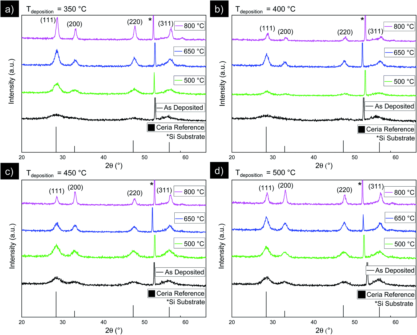 | ||
| Fig. 3 XRD of as-deposited and annealed films deposited at (a) 350 °C (b) 400 °C (c) 450 °C (d) and 500 °C. For all films, annealing causes XRD peaks to become sharper and more intense. For thin films deposited at 450 °C and 500 °C, annealing induces significant texture in favor of 〈100〉 orientations. | ||
We first investigate the as-deposited films. Fig. 2 depicts the XRD data of the as-deposited films deposited at 350 °C, 400 °C, 450 °C, and 500 °C. XRD peaks of as-deposited films are broad with low intensity, showing a slight increase in intensity and decrease in full-width half-maximum (FWHM) at higher deposition temperatures. Broad peaks with low intensity are characteristic for ceria deposited via spray pyrolysis and indicate that a significant fraction of the film is amorphous.35 The increasing intensity and sharpness of peaks for increasing deposition temperature is caused by thermally promoted nucleation and grain growth. In both Fig. 2 and 3, it is observed that the XRD peaks of the films deposited at 400 °C are generally broader than at 350 °C. We attribute this to fluctuations in film thickness, specifically that the films deposited at 400 °C are thinner than the other samples, leading to an overall weaker XRD signal.
We detail the effect of post-annealing temperature between 500 °C and 800 °C on the synthesized film microstructure with the corresponding XRD patterns in Fig. 3a–d. No cracking was observed for any of those thin films. In general, we see the following qualitative trends: firstly, increasing the deposition temperature results in slight increases in peak intensity and decrease in FWHM, and secondly, increasing the post-anneal temperature causes peak FWHM to drastically decrease by approximately 60–67% and intensity to further increase. To analyze this in more detail, we plot in Fig. 4 average grain sizes calculated using the Scherrer equation, based on the FWHM value of the (111) peak, as a function of post-annealing and deposition temperature. Strictly speaking, the Scherrer equation provides a lower bound on crystallite size. Here, we corrected for instrument peak broadening, but not for other second order effects such as micro-strain. Average grain sizes of different samples here range from 2 nm to 14 nm and increase with annealing temperature from 500 °C to 800 °C. Closer inspection reveals that we have a higher impact of post-annealing temperature than effective deposition temperature for the films. The high errors in grain size for as-deposited films are due to the nature of the low intensity, broad XRD peaks characteristic of amorphous films. At the highest annealing temperature of 800 °C, we also observe large error bars in the grain size, corresponding to fluctuations in the FWHM and intensity of different XRD peaks. We attribute this to the presence of texture which affects relative intensity, a feature that will be discussed in more detail below.
 | ||
| Fig. 4 Average grain size as a function of annealing temperature calculated using the Scherrer equation for the (111) peak. Post-annealing induces crystallization and grain growth of the largely amorphous as-deposited ceria thin films. | ||
Furthermore, the sharpening and intensification of XRD peaks with annealing temperature can also be ascribed to an increase in crystallinity. It has been demonstrated that as-deposited spray pyrolysis films tend to be primarily amorphous with small, dispersed seed crystals and fully crystallize upon annealing.30,35,36,41 Extrapolating data from a Johnson–Mehl–Avrami–Kolmogorov (JMAK) analysis of spray-pyrolysis-deposited ceria films from a previous investigation35 reveals that annealing at 500 °C for 5 hours results in a fully crystalline film if seed crystals are present as-deposited. The presence of broad, weak diffraction peaks in the as-deposited films confirms that some crystallites are present, yet the overall low signal of these peaks implies a largely amorphous structure.
In addition, the XRD data reveals interesting trends in the texture, or preferred orientation, induced by the thermal treatment of sprayed ceria thin films. For the majority of films, the (111) diffraction peak shows the highest intensity, in agreement with the randomly oriented ceria powder reference. The preference for the 〈111〉 orientation is expected due to the high stability of the (111) plane.26,42,43 However, for samples deposited at substrate temperatures of 450 °C and 500 °C, a gradual shift of the preferred orientation from the 〈111〉 to the 〈200〉 orientation is observed with annealing. Remarkably, after annealing at 800 °C, the (200) peak has the highest intensity, meaning that annealing induced texture with a preference for (200) orientation in the plane parallel to the substrate. To better quantify this phenomenon, the texture coefficients of the (200) peak, presented in Table 1 and Fig. 5, were calculated using eqn (1):
| T deposition/°C | T annealing/°C | Texture coefficient (200) | Lattice constant/nm |
|---|---|---|---|
| 350 | As deposited | — | — |
| 500 | 1.247 | 0.541 ± 0.009 | |
| 650 | 1.295 | 0.541 ± 0.010 | |
| 800 | 1.481 | 0.539 ± 0.009 | |
| 400 | As deposited | — | — |
| 500 | 1.003 | 0.541 ± 0.032 | |
| 650 | 1.338 | 0.542 ± 0.008 | |
| 800 | 1.451 | 0.538 ± 0.030 | |
| 450 | As deposited | — | — |
| 500 | 1.489 | 0.543 ± 0.006 | |
| 650 | 1.771 | 0.541 ± 0.007 | |
| 800 | 2.198 | 0.540 ± 0.006 | |
| 500 | As deposited | — | — |
| 500 | 1.487 | 0.543 ± 0.010 | |
| 650 | 1.559 | 0.542 ± 0.005 | |
| 800 | 2.016 | 0.540 ± 0.007 |
 | ||
| Fig. 5 Texture coefficients of the 〈200〉 orientation of sprayed ceria thin films for films deposited between 350 °C and 500 °C, and annealed at 500 °C, 650 °C, and 800 °C. All films exhibit a preferred 〈200〉 orientation, with films annealed at 800 °C and deposited at 450 °C and 500 °C showing a strong surprisingly large texture coefficient of 2.2 and 2.0, respectively. | ||
Texture coefficient:
 | (1) |
Because as-deposited films are mostly amorphous with only a minimal number of small crystallites, the concept of texture coefficient is not applicable, and we exclude these films from the texture coefficient analysis. Turning to the texture coefficients for films post annealed at 500 °C, we observe that films deposited at 350 °C and 400 °C have values close to 1, revealing a preference for the 〈111〉 orientation as expected from the polycrystalline ceria reference data. However, films deposited at 450 °C and 500 °C also post annealed at 500 °C have texture coefficients of approximately 1.5, indicating a significant preference to the [200] direction relative to the reference even at this low annealing temperature. As the post-annealing temperature increases for all deposition temperatures, the texture coefficient increases, reaching a value of approximately 1.5 for films deposited at 350 °C and 400 °C and 2 for films deposited at 450 °C and 500 °C. Texture coefficients of 2 indicate that we obtain films with a remarkably high texture in the [200] direction at high deposition and annealing temperatures. The majority of films here have texture coefficients greater than 1, which suggests that there is an overall stronger presence of 〈200〉 oriented grains, compared to the polycrystalline ceria reference, that increases with temperature.
Such a thermally prompted shift in preferred orientation has previously been observed on ceria thin films deposited via spray pyrolysis29,30 pulsed laser deposition,31 and electron-beam-evaporation.33 Furthermore, this shift in preferred orientation appears to be independent of the substrate, as it was also observed for thin films deposited on MgO (see ESI†). This is in agreement with some reports in the literature, where such texture has been observed in ceria films deposited on sapphire substrates45 and on ceria nanoparticles deposited on Ru(0001).25 However, the reason for this prevalence of the (200) peak with increasing processing temperatures has been a point of speculation, as the (200) surface has been shown to be unstable due to its relatively high surface energy and net dipole moment arising from its arrangement of alternately charged planes.42 Several density functional studies have confirmed that the ordering of surface energies of the low index ceria planes from highest energy to lowest energy is: {100} > {110} > {111}.26,27 Consequently, the transition from 〈111〉 to 〈200〉 oriented films is expected to be energetically unfavorable and unstable; one would expect that upon annealing, films would relax to the most energetically favorable configuration. Therefore, our experimental results reported here indicate that the energetics calculated in these studies must be incomplete. Recent studies have identified the emergence of {100} terminated facets in ceria nanoparticles25,32 and 〈100〉 preferred orientations in thin films31,45 upon thermal treatment. It has been suggested that surface defects,32 such as oxygen ion vacancies,25 impurities, or surface reconstructions46 may facilitate the stabilization of {100} surfaces. In a computational study on {100} terminated ceria surfaces, it was determined using density functional theory that various reconstructions of the {100} surface could become energetically favorable at lower oxygen partial pressures by the formation of oxygen defects.25 Annealing films that were deposited at higher temperatures may provide the required energy needed to reconstruct or form oxygen vacancies at the surface. However, in the present study, annealing was conducted under stagnant air and not under reducing conditions as described in ref. 25. Therefore, the analysis only provides a partial explanation for how 〈200〉 oriented films could be stabilized and energetically favorable, as this study shows that a preferred (200) texture is induced at ambient oxygen partial pressures. Therefore, further theoretical studies are required to fully determine the energetics of surface orientation and texture in ceria and explain the preferred (200) texture observed here.
Understanding how to tune ceria processing such that the {100} facets are prevalent is appealing for catalyst applications and a point of active research. {100} surfaces have been demonstrated experimentally and computationally to have higher catalytic performance and activity28,47 than {111} surfaces as a result of the higher surface energy of {100} surfaces, which leads to more favorable oxygen vacancy formation energetics, and in turn a higher affinity to participate in oxygen-exchanging reactions. Therefore, the simple method of controlling film texture with a preferred 〈100〉 orientation presented here shows promise in controlling and engineering catalytic surface activity of ceria.
To complete the XRD analysis, we turn to the lattice parameter, which can be useful in detecting lattice strain. Table 1 shows the lattice parameter at each deposition and annealing temperature. Lattice parameters range from 0.539 nm to 0.542 nm which is close to the fully relaxed value 0.541 nm for ceria.48 Slight fluctuations in lattice parameters are seen, yet there is no clear trend with annealing or deposition temperatures. While this implies the presence of some degree of lattice strain, the lack of trend with temperature shows that it is likely not thermally induced.
Raman analysis
To complement the XRD film microstructure analysis, we turn to Raman spectroscopy, which can provide deeper insight into the short-range order, bonding, and strain within a solid. Due to its cubic symmetry, the only Raman active mode for pure, stoichiometric ceria is the triply degenerate F2g stretching mode. This mode corresponds to the so-called oxygen breathing mode, i.e., the bond vibrations between the cerium ion and eight tetrahedrally coordinated oxygen ions in the cubic fluorite structure, which appears at a 465 cm−1 wavenumber for bulk ceria.13Fig. 6 displays Raman spectra of films deposited at 350 °C and post-annealed at 500 °C, 650 °C, and 800 °C on MgO substrates. In each spectrum, the F2g mode is present, and for the as-deposited film, several additional peaks are observed at wavenumbers ranging between 600 cm−1 and 1500 cm−1. The Raman spectrum of bis 2-ethyl hexyl phthalate, the highest-boiling point organic component of the spray pyrolysis precursors, is displayed for reference of comparison to the as-deposited film. Overlapping peaks between the two spectra can be observed, suggesting that the additional peaks in the as-deposited film can be attributed to organic residues from the precursor. Interestingly, we only detect organic residues in the Raman spectrum for the film as deposited at 350 °C, which implies that at higher annealing and deposition temperatures organic residues further decompose and evaporate from the film, becoming undetectable for Raman spectroscopy. The presence of these organic Raman peaks confirms that the organic precursor becomes incorporated into the amorphous–crystalline film structure for films as-deposited at 350 °C. To the best of our knowledge, Raman has not been used before to clearly detect organic precursor residues in spray pyrolysis films. Controlling the amount of organic precursor residue is useful in situations where impurities could impact film functionality. For instance, ceria can be employed as a low temperature proton conductor,49 so having organic residues within the film could be beneficial in potentially increasing the protonic defect density and thereby proton conductivity. Scherrer et al. observed that proton conductivity in certain YSZ thin films deposited via spray pyrolysis was affected by the presence of organic residues.50 This gives a first indication that organic residues can serve as a source for excess protons in fluorite-structured oxides such as ceria or YSZ, but further studies have to be performed to explore the impact of organic residues on proton conductivity in oxides in more detail. | ||
| Fig. 6 Raman spectra of a sprayed film as-deposited at 350 °C and annealed at 500 °C, 650 °C, and 800 °C. All films show sharp F2g Raman peaks, and the film as deposited shows a signature of the organic precursor, indicating that organic precursor was incorporated into the film during deposition. | ||
Fig. 7 displays Raman spectra around the F2g mode for each deposition and annealing temperature, for further analysis of this characteristic Raman peak. For all spectra, except for the as-deposited film at 400 °C, the F2g peak is present. The overall peak intensity was weak due to the low thickness of the films, and for the film as-deposited at 400 °C, no F2g peak was observed, likely due to the weak signal of this thin film. Due to film thickness variations and instrument limitations on focusing quality during measurements, relative peak intensities fluctuated greatly, so we cannot draw any conclusions from peak intensity. As-deposited peaks are relatively broad, due to their amorphous microstructure. The lack of periodicity in an amorphous solid results in lattice vibrations that are more disordered and differ from the phonons of a crystalline solid. This impacts Raman scattering, causing broader Raman peaks with an asymmetric line shape.51 As annealing temperature increases, peaks narrow, indicating a transition from amorphous to crystalline microstructures52 and grain growth,53 agreeing with XRD results. Furthermore, changes in the F2g Raman mode position with annealing are observed. This is shown in Fig. 8 where the F2g mode position is plotted against annealing temperature and listed in Table 2. We classify two regions of F2g peak positions: Region I (shaded in gray) and Region II, being below 465 cm−1 and above 465 cm−1, respectively.
 | ||
| Fig. 7 Raman spectra of the F2g peak of as-deposited and annealed films deposited at (a) 350 °C, (b) 400 °C, (c) 450 °C, (d) and 500 °C. | ||
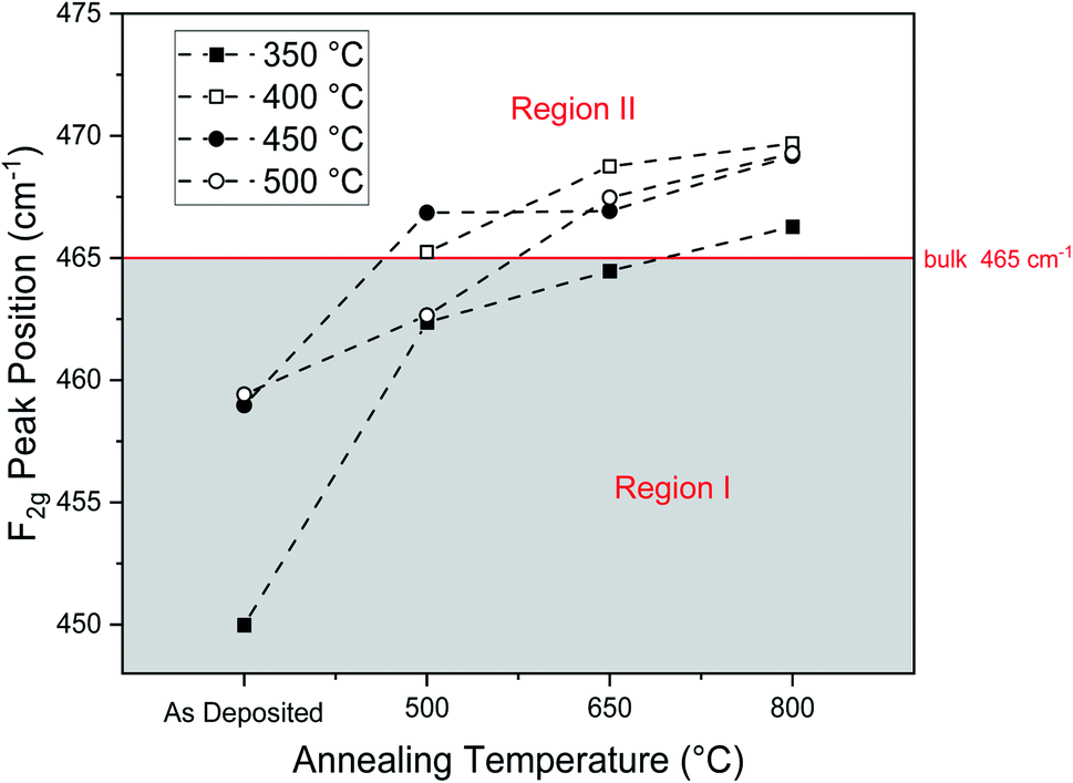 | ||
| Fig. 8 F2g Raman peaks positions as a function of annealing temperature. Two regions are observed in the Raman F2g peak position. Region I: for as-deposited films and some films annealed at 500 °C, the F2g peak is below the bulk ceria value of 465 cm−1. Region II: high temperature annealed films show a F2g peak position above 465 cm−1. | ||
| T deposition/°C | T annealing/°C | F2g peak position/cm−1 |
|---|---|---|
| 350 | As deposited | 450 |
| 500 | 462 | |
| 650 | 464 | |
| 800 | 466 | |
| 400 | As deposited | Peak not visible |
| 500 | 465 | |
| 650 | 469 | |
| 800 | 470 | |
| 450 | As deposited | 459 |
| 500 | 467 | |
| 650 | 467 | |
| 800 | 469 | |
| 500 | As deposited | 459 |
| 500 | 463 | |
| 650 | 467 | |
| 800 | 469 |
In Region I, F2g mode positions of as-deposited films are significantly below the characteristic bulk value of 465 cm−1, with a general trend of increasing F2g wavenumber with increasing post-anneal temperature. As established by XRD results, as-deposited films at all deposition temperatures exhibit a significant fraction of amorphous microstructure. Because annealing increases both grain size and crystallinity, a combination of these features prompts the general increase Raman mode frequency with annealing up to the bulk standard of 465 cm−1.
The observation that for all as-deposited samples where an F2g peak was present, the F2g peak position was significantly lower than the expected bulk value of 465 cm−1 is expected: The amorphous structure is generally more disordered and has longer average cerium–oxygen bonds than the crystalline phase, which results in a lowered F2g mode frequency for the largely amorphous as-deposited films. Additionally, the film as-deposited at 350 °C stands out with a notably low F2g wavenumber of 450 cm−1. While this low wavenumber can in part be attributed to its largely amorphous microstructure with a small number of dispersed nano-crystallites, it is also important to note that the film as-deposited at 350 °C was the only one to exhibit Raman-active organic precursor residues. The incorporation of organic precursor residues as space-filler in the structure of ceria films increases the cerium–oxygen bond distance, resulting in a lower F2g mode frequency. As the residues evaporate during annealing, space in the film where residues resided is freed, allowing for closer packing of the cerium and oxygen ions and consequently an increase in F2g mode frequency with annealing. Similar arguments have been made elsewhere that organic residues from the spray pyrolysis precursor can become incorporated into the film structure and result in a less compact structural packing.38
Four additional annealed films in Region I exhibit Raman peaks at or below the bulk peak position of 465 cm−1. As shown from the XRD analysis in the previous section, particle size within thin films here is in the range of a few nanometers and increases with annealing temperature. It is well-known that for nanocrystalline ceria the F2g peak is shifted to lower wave numbers compared to bulk ceria and that this shift increases with decreasing grain size.38,53–55 This phenomenon is due to phonon confinement: when grain-size is on the nanoscale, phonons become constrained within the small grains, resulting in Raman peaks at lower frequencies with more asymmetric broadening compared to in the bulk state.56–58 Therefore, given the particle size at the order of 5–10 nm for these films, phonon confinement can well explain the F2g peak shift below the bulk ceria reference and the increase in wavenumber of this shift with increasing annealing temperature.
While there is general agreement in literature regarding the trends observed in Region I, the results from Region II are more surprising. In Region II, the F2g mode similarly increases with annealing temperature. However, the F2g peak exceeds the 465 cm−1 bulk value, reaching values around 470 cm−1 for films deposited at 400 °C, 450 °C, and 500 °C and post-annealed at 800 °C. Such drastic changes in Raman shift and high F2g mode frequencies are often indicative of lattice strain, which is particularly prominent in thin films. In literature, changes in F2g mode frequencies on the scale shown here have been a result of chemical strain from doping,59 physically applied strain,60 and strain from the substrate15 in thin films. However, films here are undoped, no external stress is applied, and the deposition of amorphous ceria with subsequent crystallization indicates that the substrate should not influence the strain either. Turning to the lattice parameters obtained from XRD measurements, Table 1, the macroscopic strain in all thin films is small and without a clear trend, which is inconsistent with the clear increase in F2g frequency with annealing temperature. One would expect the lattice parameter to decrease with increasing Raman shift, as outlined by the Grüneisen parameter, which characterizes the correlation between lattice volume and vibrational frequency.13 Raman shift is directly related to bond strength, which increases with decreasing bond length. Therefore, a noticeable decrease in lattice volume would be expected for such a drastic increase in F2g frequency, which is however not observed in the long-range order as measured by XRD. In addition, we confirmed via XRD that there is no difference in the observed long-range order in thin films deposited on both the Si/Si3N4 substrates and the MgO substrates, as shown in the ESI (ESI 4†). In addition, it is highly unlikely that the present observations of induced texture and an apparent correlation with the Raman peak position are caused by trace impurity diffusion. First of all, the preferred orientation was observed for both the MgO and Si/Si3N4 substrates, i.e., the effect is independent of the underlying substrate. In particular, amorphous Si3N4 is an excellent diffusion barrier and highly thermally stable, and to the best of the authors' knowledge, there are no reports of significant Si diffusion from Si3N4 into ceria at the relatively low annealing temperatures of this study, between 350 °C and 800 °C. In addition, no extrinsic impurity peaks were observed under Raman, which would be expected for the solid solution formation or grain boundary diffusion of trace elements.17
A recent study on epitaxially grown ceria has observed that apparent peak shifts toward higher Raman wavenumbers in ceria may be caused by breaks of crystal symmetry, and that the apparent Raman shift is actually a peak splitting of the triply degenerate F2g mode.61 However, this peak splitting should be detectable under polarized Raman spectroscopy, and we did not find any effect of polarization on the measured Raman peak position in this present study.
Interestingly, we observe a correlation between the F2g peak position and the orientation of the grains, viz. the texture coefficient, as shown in Fig. 9. Both parameters, the F2g peak position and the texture coefficient, increase with increasing annealing temperature. We observe that for samples annealed at 500 °C, the F2g peak position is close to the bulk value of 465 cm−1, and the (200) texture coefficient is close to 1. Therefore, samples annealed at 500 °C exhibit structural properties in agreement with the literature of equilibrated, stoichiometric cerium oxide.17 In contrast, for samples annealed at 650 °C and 800 °C, we observe significant texture in favor of the 〈100〉 orientation, as well as high Raman F2g wavenumbers between 465 cm−1 and 470 cm−1. This suggests that the increase in texture for the 〈100〉 orientation with annealing may cause a decrease in the cerium–oxygen bond length at the near order within the thin film surface or volume. Similar to the work by Sediva et al.,61 it can be hypothesized that a symmetry break, in this case in the form of induced texture, induces a Raman peak shift toward higher wave numbers which cannot be explained by other effects such as phonon confinement or local defects. This is a first indication that Raman spectroscopy could be used to measure thin film texture in ceria.
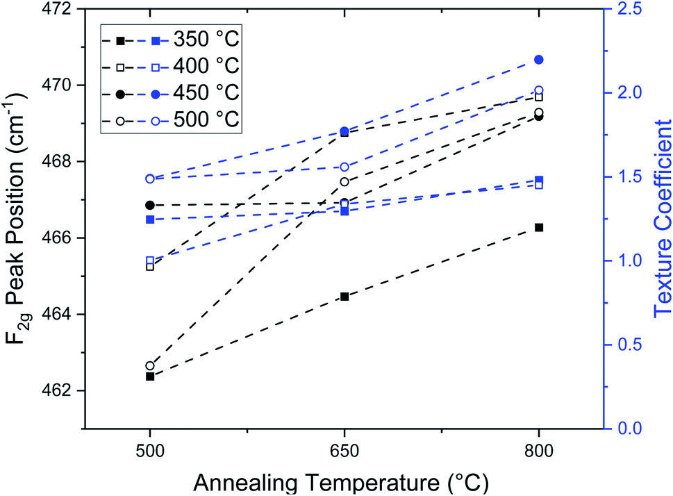 | ||
| Fig. 9 F2g Raman peaks positions as a function of annealing temperature, for annealed thin films. The Raman F2g peak position is correlated with the increasing (200) texture coefficient observed in annealed ceria thin films. | ||
Conclusions
Spray pyrolysis is a promising method to deposit inexpensive ceramic thin film coatings with good control over microstructure and crystallinity. In particular, spray pyrolysis can be used to deposit ceria, which has particular importance as a catalyst material for solid oxide fuel cells, solar fuel conversion, and as an oxygen buffer in three-way catalysis. In this paper, we provide specific processing guidelines for the deposition of ceria thin films using spray pyrolysis, and study the effect of thermal processing on the orientation of sprayed ceria thin films, an important feature for catalytic applications. We consider what are the upper limits to deposit dense films under the complex interplay of solvent evaporation and ceria crystallization, and find that the critical thickness above which films cracked to be 300 nm. Understanding how to prevent crack formation is crucial when integrating spray pyrolysis deposited films into devices where crack formation hinders performance.We newly report crystal texture data across a wide range of deposition and post-annealing temperatures, and find that a preferred orientation detected in XRD correlates to unusual peak shifts of the Raman F2g oxygen breathing mode to higher wavenumbers. We find that the energetically unfavorable, but highly catalytically active 〈100〉 orientation becomes preferred after thermal annealing, and that Raman spectroscopy can be a useful, accessible tool to detect such orientation evolution for catalysis research.
Collectively, this contributes to the fundamentals understanding of ceramic synthesis by spray pyrolysis, and specifically on the material class of ceria. In addition, it provides a cost-effective method to vary future catalyst coatings of ceria with orientations to control their functionality. For this we identify a new correlation between the F2g Raman stretching mode and crystal orientation that can be used as a marker for future designs of thin film deposition pathways and catalytic coatings.
Author contributions
PS and KPT contributed equally to this work. PS and JLMR conceptualized the work. PS and KPT performed the experiments and data analysis. JLMR provided guidance for the research. All authors contributed to writing and revising the manuscript.Conflicts of interest
The authors declare no conflict of interest.Acknowledgements
This work made use of the MRSEC Shared Experimental Facilities at MIT, supported by the National Science Foundation under award number DMR-1419807. This work was performed in part at the Center for Nanoscale Systems (CNS), a member of the National Nanotechnology Coordinated Infrastructure Network (NNCI), which is supported by the National Science Foundation under NSF award no. 1541959. CNS is part of Harvard University. K. P. Torres thanks MIT's Undergraduate Research Opportunities Program for financial support. P.S. gratefully acknowledges financial support through the Broshy Graduate Fellowship and Hugh Hampton Young Memorial Fund Fellowship at MIT and through Merck KGaA, Darmstadt, Germany. J. L. M. R. thanks the Thomas Lord Foundation for financial support.References
- J. B. Park, J. Graciani, J. Evans, D. Stacchiola, S. Ma, P. Liu, A. Nambu, J. F. Sanz, J. Hrbek and J. A. Rodriguez, Proc. Natl. Acad. Sci. U. S. A., 2009, 106, 4975–4980 CrossRef CAS PubMed.
- Q. Fu, A. Weber and M. Flytzani-Stephanopoulos, Catal. Lett., 2001, 77, 87–95 CrossRef CAS.
- A. Trovarelli, Catal. Rev. – Sci. Eng., 1996, 38, 439–520 CrossRef CAS.
- W. C. Chueh, Y. Hao, W. Jung and S. M. Haile, Nat. Mater., 2012, 11, 155–161 CrossRef CAS PubMed.
- Y. Shi, A. H. Bork, S. Schweiger and J. L. M. Rupp, Nat. Mater., 2015, 14, 721–727 CrossRef CAS PubMed.
- W. C. Chueh, C. Falter, M. Abbott, D. Scipio, P. Furler, S. M. Haile and A. Steinfeld, Science, 2010, 330, 1797–1801 CrossRef CAS PubMed.
- E. Sediva, A. J. Carrillo, C. E. Halloran and J. L. M. Rupp, ACS Appl. Energy Mater., 2021, 4, 1474–1483 CrossRef CAS.
- A. H. Bork, A. J. Carrillo, Z. D. Hood, B. Yildiz and J. L. M. Rupp, ACS Appl. Mater. Interfaces, 2020, 12, 32622–32632 CrossRef CAS PubMed.
- R. Schmitt, J. Spring, R. Korobko and J. L. M. Rupp, ACS Nano, 2017, 11, 8881–8891 CrossRef CAS PubMed.
- S. Schweiger, R. Pfenninger, W. J. Bowman, U. Aschauer and J. L. M. Rupp, Adv. Mater., 2017, 29, 1605049 CrossRef PubMed.
- T. Montini, M. Melchionna, M. Monai and P. Fornasiero, Chem. Rev., 2016, 116, 5987–6041 CrossRef CAS PubMed.
- M. Mogensen, N. M. Sammes and G. A. Tompsett, Solid State Ionics, 2000, 129, 63–94 CrossRef CAS.
- R. Schmitt, A. Nenning, O. Kraynis, R. Korobko, A. I. Frenkel, I. Lubomirsky, S. M. Haile and J. L. M. Rupp, Chem. Soc. Rev., 2020, 49, 554–592 RSC.
- H. L. Tuller and S. R. Bishop, Annu. Rev. Mater. Res., 2011, 41, 369–398 CrossRef CAS.
- O. Kraynis, E. Makagon, E. Mishuk, M. Hartstein, E. Wachtel, I. Lubomirsky and T. Livneh, Adv. Funct. Mater., 2019, 29, 1804433 CrossRef.
- J. L. M. Rupp, E. Fabbri, D. Marrocchelli, J. W. Han, D. Chen, E. Traversa, H. L. Tuller and B. Yildiz, Adv. Funct. Mater., 2014, 24, 1562–1574 CrossRef CAS.
- R. Schmitt, A. Nenning, O. Kraynis, R. Korobko, A. I. Frenkel, I. Lubomirsky, S. M. Haile and J. L. M. Rupp, Chem. Soc. Rev., 2020, 49, 554–592 RSC.
- S. Schweiger, M. Kubicek, F. Messerschmitt, C. Murer and J. L. M. Rupp, ACS Nano, 2014, 8, 5032–5048 CrossRef CAS PubMed.
- Y. Shi, I. Garbayo, P. Muralt and J. L. Marguerite Rupp, J. Mater. Chem. A, 2017, 5, 3900–3908 RSC.
- R. Korobko, A. Patlolla, A. Kossoy, E. Wachtel, H. L. Tuller, A. I. Frenkel and I. Lubomirsky, Adv. Mater., 2012, 24, 5857–5861 CrossRef CAS PubMed.
- R. Korobko, A. Lerner, Y. Li, E. Wachtel, A. I. Frenkel and I. Lubomirsky, Appl. Phys. Lett., 2015, 106, 042904 CrossRef.
- E. Makagon, E. Wachtel, L. Houben, S. R. Cohen, Y. Li, J. Li, A. I. Frenkel and I. Lubomirsky, Adv. Funct. Mater., 2021, 31, 2006712 CrossRef CAS.
- Y. M. Chiang, E. B. Lavik, I. Kosacki, H. L. Tuller and J. Y. Ying, Appl. Phys. Lett., 1996, 69, 185–187 CrossRef CAS.
- K. Zhou, X. Wang, X. Sun, Q. Peng and Y. Li, J. Catal., 2005, 229, 206–212 CrossRef CAS.
- Y. Pan, N. Nilius, C. Stiehler, H. J. Freund, J. Goniakowski and C. Noguera, Adv. Mater. Interfaces, 2014, 1, 1400404 CrossRef.
- Y. Jiang, J. B. Adams and M. Van Schilfgaarde, J. Chem. Phys., 2005, 123, 064701 CrossRef PubMed.
- D. Marrocchelli and B. Yildiz, J. Phys. Chem. C, 2012, 116, 2411–2424 CrossRef CAS.
- T. S. Sreeremya, A. Krishnan, K. C. Remani, K. R. Patil, D. F. Brougham and S. Ghosh, ACS Appl. Mater. Interfaces, 2015, 7, 8545–8555 CrossRef CAS PubMed.
- A. K. B. Elidrissia, M. Addoua, M. Regraguia, C. Montyb, A. Bougrinea and A. Laboratoire, Thin Solid Films, 2000, 379, 23–27 CrossRef.
- J. L. M. Rupp, C. Solenthaler, P. Gasser, U. P. Muecke and L. J. Gauckler, Acta Mater., 2007, 55, 3505–3512 CrossRef CAS.
- G. Balakrishnan, S. T. Sundari, P. Kuppusami, P. C. Mohan, M. P. Srinivasan, E. Mohandas, V. Ganesan and D. Sastikumar, Thin Solid Films, 2011, 519, 2520–2526 CrossRef CAS.
- L. Y. Kuo and P. Shen, Mater. Sci. Eng., A, 2000, 277, 258–265 CrossRef.
- M. S. AI-Robaee, L. Shivalingappa, K. Narasimha Rao and S. Mohan, Thin Solid Films, 1992, 221, 214–219 CrossRef.
- D. Beckel, A. Bieberle-Hütter, A. Harvey, A. Infortuna, U. P. Muecke, M. Prestat, J. L. M. Rupp and L. J. Gauckler, J. Power Sources, 2007, 173, 325–345 CrossRef CAS.
- J. L. M. Rupp, B. Scherrer, A. S. Harvey and L. J. Gauckler, Adv. Funct. Mater., 2009, 19, 2790–2799 CrossRef CAS.
- B. Scherrer, S. Heiroth, R. Hafner, J. Martynczuk, A. Bieberle-Hütter, J. L. M. Rupp and L. J. Gauckler, Adv. Funct. Mater., 2011, 21, 3967–3975 CrossRef CAS.
- S. S. Dana, K. F. Etzold and J. Clabes, J. Appl. Phys., 1991, 69, 4398–4403 CrossRef CAS.
- J. L. M. Rupp, B. Scherrer and L. J. Gauckler, Phys. Chem. Chem. Phys., 2010, 12, 11114–11124 RSC.
- A. A. Griffith, Philos. Trans. R. Soc., A, 1920, 221, 163–198 Search PubMed.
- J. Li, A. K. Dozier, Y. Li, F. Yang and Y.-T. Cheng, J. Electrochem. Soc., 2011, 158, A689 CrossRef CAS.
- B. Scherrer, J. Martynczuk, H. Galinski, J. G. Grolig, S. Binder, A. Bieberle-Hütter, J. L. M. Rupp, M. Prestat and L. J. Gauckler, Adv. Funct. Mater., 2012, 22, 3509–3518 CrossRef CAS.
- P. W. Tasker, J. Phys. C: Solid State Phys., 1979, 12, 4977–4984 CrossRef CAS.
- T. X. T. Sayle, S. C. Parker and C. R. A. Catlow, Surf. Sci., 1994, 316, 329–336 CrossRef CAS.
- S. Gates-Rector and T. Blanton, Powder Diffr., 2019, 34, 352–360 CrossRef CAS.
- T. Suzuki, I. Kosacki, H. U. Anderson and P. Colomban, J. Am. Ceram. Soc., 2001, 84, 2007–2014 CrossRef CAS.
- D. C. Sayle, S. A. Maicaneanu and G. W. Watson, J. Am. Chem. Soc., 2002, 124, 11429–11439 CrossRef CAS PubMed.
- E. Aneggi, J. Llorca, M. Boaro and A. Trovarelli, J. Catal., 2005, 234, 88–95 CrossRef CAS.
- L. Gerward, J. Staun Olsen, L. Petit, G. Vaitheeswaran, V. Kanchana and A. Svane, J. Alloys Compd., 2005, 400, 56–61 CrossRef CAS.
- P. Simons, K. P. Torres and J. L. M. Rupp, Adv. Funct. Mater., 2021, 31, 2009630 CrossRef CAS.
- B. Scherrer, M. V. F. Schlupp, D. Stender, J. Martynczuk, J. G. Grolig, H. Ma, P. Kocher, T. Lippert, M. Prestat and L. J. Gauckler, Adv. Funct. Mater., 2013, 23, 1957–1964 CrossRef CAS.
- P. Yogi, M. Tanwar, S. K. Saxena, S. Mishra, D. K. Pathak, A. Chaudhary, P. R. Sagdeo and R. Kumar, Anal. Chem., 2018, 90, 8123–8129 CrossRef CAS PubMed.
- G. Gouadec and P. Colomban, Prog. Cryst. Growth Charact. Mater., 2007, 53, 1–56 CrossRef CAS.
- S. Saitzek, J. F. Blach, S. Villain and J. R. Gavarri, Phys. Status Solidi A, 2008, 205, 1534–1539 CrossRef CAS.
- F. Zhang, S. W. Chan, J. E. Spanier, E. Apak, Q. Jin, R. D. Robinson and I. P. Herman, Appl. Phys. Lett., 2002, 80, 127–129 CrossRef CAS.
- I. O. Mazali, B. C. Viana, O. L. Alves, J. Mendes Filho and A. G. Souza Filho, J. Phys. Chem. Solids, 2007, 68, 622–627 CrossRef CAS.
- H. Richter, Z. P. Wang and L. Ley, Solid State Commun., 1981, 39, 625–629 CrossRef CAS.
- A. K. Arora, M. Rajalakshmi, T. R. Ravindran and V. Sivasubramanian, J. Raman Spectrosc., 2007, 38, 604–617 CrossRef CAS.
- Z. V. Popović, Z. Dohčević-Mitrović, M. Ŝćepanović, M. Grujić-Brojčin and S. Aŝkrabić, Ann. Phys, 2011, 523, 62–74 CrossRef.
- J. L. M. Rupp, E. Fabbri, D. Marrocchelli, J. W. Han, D. Chen, E. Traversa, H. L. Tuller and B. Yildiz, Adv. Funct. Mater., 2014, 24, 1562–1574 CrossRef CAS.
- H. Li, P. Zhang, G. Li, J. Lu, Q. Wu and Y. Gu, J. Alloys Compd., 2016, 682, 132–137 CrossRef CAS.
- E. Sediva, D. Bohdanov, G. F. Harrington, I. Rafalovskyi, J. Drahokoupil, F. Borodavka, P. Marton and J. Hlinka, ACS Appl. Mater. Interfaces, 2020, 12, 56251–56259 CrossRef CAS PubMed.
Footnotes |
| † Electronic supplementary information (ESI) available. See DOI: 10.1039/d1ta09115h |
| ‡ The authors contributed equally to this manuscript. |
| This journal is © The Royal Society of Chemistry 2022 |