
 Open Access Article
 This Open Access Article is licensed under a
 Creative Commons Attribution 3.0 Unported Licence
High ionic conductivity in fluorite δ-bismuth oxide-based vertically aligned nanocomposite thin films†
Adam J.
Lovett
 *a,
Matthew P.
Wells
a,
Zihao
He
b,
Juanjuan
Lu
b,
Haiyan
Wang
bc and
Judith L.
MacManus-Driscoll
a
*a,
Matthew P.
Wells
a,
Zihao
He
b,
Juanjuan
Lu
b,
Haiyan
Wang
bc and
Judith L.
MacManus-Driscoll
a
aDepartment of Materials Science and Metallurgy, University of Cambridge, 27 Charles Babbage Road, Cambridge CB3 0FS, UK. E-mail: ajl207@cam.ac.uk
bSchool of Electrical Engineering, Purdue University, 701 West Stadium Avenue, West Lafayette 47907-2045, USA
cSchool of Materials Engineering, Purdue University, 701 West Stadium Avenue, West Lafayette 47907-2045, USA
First published on 3rd February 2022
Abstract
δ-Bi2O3 has long been touted as a potential material for use in solid oxide fuel cells (SOFC) due to its intrinsically high ionic conductivity. However, its limited operational temperature has led to stabilising the phase from >725 °C to room temperature either by doping, albeit with a compromise in conductivity, or by growing the phase confined within superlattice thin films. Superlattice architectures are challenging to implement in functional μSOFC devices owing to their ionic conducting channels being in the plane of the film. Vertically aligned nanocomposites (VANs) have the potential to overcome these limitations, as their nanocolumnar structures are perpendicular to the plane of the film, hence connecting the electrodes at top and bottom. Here, we demonstrate for the first time the growth of epitaxially stabilised δ-Bi2O3 in VAN films, stabilised independently of substrate strain. The phase is doped with Dy and is formed in a VAN film which incorporates DyMnO3 as a vertically epitaxially stabilising matrix phase. Our VAN films exhibit very high ionic conductivity, reaching 10−3 S cm−1 at 500 °C. This work opens up the possibility to incorporate thin film δ-Bi2O3 based VANs into functional μSOFC devices, either as cathodes (by pairing δ-Bi2O3 with a catalytically active electronic conductor) and/or electrolytes (by incorporating δ-Bi2O3 with an insulator).
Preface
We are delighted to write this article to honour the long and distinguished career of Prof. John Kilner (JK). Judith MacManus-Driscoll (JLM-D), the last author of this article, first met JK in 1985 when she was an undergraduate at Imperial College London. JK was, at the time, working very closely with Brian Steele who connected JLM-D with the ionics field, via 2 summer internships with the ionic groups at the Max Planck Institute FKF. JLM-D then undertook her final year undergraduate research project working on studying the ionic conductivity and diffusivity of oxygen in δ-Bi2O3. Thanks to JK, within a few short weeks excellent results came out. At the same time, JK's outstanding lectures on transition metal oxides (JLM-D recalls references to the pioneering work of John Goodenough on the electronic structure of transition metal oxides) and on the excitement of the discovery of high temperature superconductivity in cuprates spurred JLM-D to do a PhD in that area. Upon receiving this invitation to write a paper to honour JK's distinguished career, JLM-D, her team, and collaborators had the perfect opportunity to revisit δ-Bi2O3, after a nearly 35 year break. In presenting this work, we thank JK for his great dedication and pioneering work in the ionics field and beyond. We aim to convince the reader that δ-Bi2O3 can be stabilised from >725 °C down to room temperature in thin films using the vertically aligned nanocomposite (VAN) approach.Introduction
To this day, cubic fluorite δ-Bi2O3 remains the highest ionic conducting material of all known oxygen ion conductors, achieving 1 S cm−1 at 730 °C, up to two orders of magnitude higher conductivity than the industrial standard yttria stabilized zirconia oxide (YSZ).1,2 This high ionic conductivity is attributed to the inherent defect structures with 25% oxygen vacancy concentration, the weak Bi–O bond and high polarizability of the Bi3+ ion.3 However, δ-Bi2O3 has a limited operational temperature range in SOFC and ionic devices, melting above 823 °C, and undergoing a phase transition to the monoclinic α-phase below 730 °C, resulting in a greatly reduced conductivity.2 Many studies have demonstrated the fluorite phase can be stabilised to room temperature with carefully selected dopants, predominantly trivalent lanthanides, but this comes at the expense of a reduction in the ionic conductivity, by up to 4 orders of magnitude.2,4–6 Extensive research effort has been focused on finding the optimum dopant and concentration required to stabilise the fluorite phase, and maximise ionic conductivity.1,2,4,5,7An alternative approach to stabilising the δ-Bi2O3 phase is the growth of epitaxial thin films on single-crystal substrates that promote the fluorite structure. Epitaxial pulsed laser deposition (PLD) films have been successfully grown on Al2O3, SrTiO3 and MgO.8–10 However, for epitaxial films, substrate strain relaxation occurs above a few 10's of nm11 and this limits the structural robustness of the δ-Bi2O3. In fact, heat treatment of Er stabilised δ-Bi2O3 (ESB) thin films on MgO resulted in polycrystalline rearrangement,8 which could pose limitations in performance and cyclability if implemented in μSOFC devices. Epitaxial stabilisation has also been demonstrated in superlattices. Here, Sanna et al. stabilised δ-Bi2O3 by growing superlattice films with extremely thin (<3 nm) layers of fluorite Bi2O3 grown between a supporting layers.12,13 Two extraordinary features came out of the aforementioned work: (1) [ESB/Ce0.8Gd0.2O2−δ] superlattices are very stable under severe reducing conditions whilst retaining high conductivity; (2) it is possible to grow [δ-Bi2O3/YSZ] superlattices free of a fluorite stabilising dopant, facilitating the possibility of accessing the higher conductivities of undoped δ-Bi2O3 at lower temperatures. Whilst remarkable, as already noted, the ionic conducting channels are confined to the plane of the film, whereas the ion transport needs to be out-of-the-plane to connect ion transport with top and bottom electrodes in a practical device architecture.14
An alternative to superlattice films is vertically aligned nanocomposite (VAN) films. These films consist of many columns with typically 10–50 nanometre diameters embedded in a film matrix. Not only are they simpler to grow than superlattice films, but VANs have also displayed enhanced conductivity, reduced areal surface resistances (ASR) and improved μSOFC performances.15–18 Crucially, due to their conducting channels lying perpendicular to the substrate, the 3D VAN architecture can be incorporated into functional nanoionic devices.
Here, we demonstrate that it is possible to stabilise the δ-Bi2O3 phase to room temperature by encapsulating it in an epitaxial VAN structure grown on the widely available SrTiO3 (STO)/Nb-doped SrTiO3 (Nb-STO) single crystal substrates. We grow Dy stabilised δ-Bi2O3-DyMnO3 VAN films (herein referred to as DSB-DMO), dysprosium being chosen as it; (a) DyMnO3 adopts the GdFeO3 perovskite structure, which as we later discuss plays an important role in stabilising the δ-fluorite phase; (b) DSB has very high ionic conductivity with the lowest conductivity degradation when aged,1,3 a known phenomenon in stabilised δ-Bi2O3. Our results confirm the presence of Dy stabilised δ-Bi2O3 nanocolumns, clearly phase separated from a DyMnO3 matrix in VAN films, and we observe exceptional ionic conductivity, competitive with the highest reported in literature to date. These results may provide a platform for developing δ-Bi2O3 VAN systems for μSOFC applications, taking advantage of the superior ionic conductivity and fast oxygen surface kinetics of the δ-Bi2O3 phase in a stable and simple-to-grow VAN film.19,20
Experimental
DSB/DMO synthesis and target preparation
Stoichiometric ratios of Dy2O3, Mn2O3 for DyMnO3, and Bi2O3, Dy2O3 for (Dy2O3)0.25(Bi2O3)0.75 were ball milled in ethanol. DMO and DSB were reacted using the solid-state method at 1673 K and 1073 K respectively. A composite target was prepared by mixing synthesised DSB and DMO in a 1![[thin space (1/6-em)]](https://www.rsc.org/images/entities/char_2009.gif) :1 ratio by volume, pelletising and sintering at 1073 K for 10 h, with 10% wt. excess of Bi2–O3 added to compensate for bismuth loss during PLD.
:1 ratio by volume, pelletising and sintering at 1073 K for 10 h, with 10% wt. excess of Bi2–O3 added to compensate for bismuth loss during PLD.
PLD experiments
Films were grown by pulsed laser deposition (PLD) using a KrF excimer laser with a wavelength of 248 nm. Before growth, (001) orientated SrTiO3/Nb-doped SrTiO3 (0.5% wt. Nb, 5 × 5 × 0.5 mm) substrates were cleaned sequentially in acetone, propan-2-ol, and deionised water in an ultrasonic bath for 5 minutes. Prior to deposition, the chamber was evacuated to at least 3 × 10⁻⁶ mbar before filling to a growth pressure of 0.13 mbar O2 with a flow rate of 6 sccm. The target was pre-ablated for 3 minutes with a fluence of 0.8 J cm−2 at 5 Hz. Films were grown on with the following growth conditions: Tsub = 973 K, F = 0.8 J cm−2, pO2 = 0.13 mbar, ν = 5 Hz.XRD characterisation
Films were characterised with high resolution X-ray diffraction (XRD), performed on a Panalytical Empyrean vertical diffractometer using a Cu Kα X-ray radiation source with a wavelength of 1.5418 Å.TEM
Film microstructure was characterized by transmission electron microscopy (TEM), high-angle annular dark field scanning transmission electron microscopy (HAADF-STEM), and energy-dispersive X-ray spectroscopy (EDS) (Thermo Fisher Scientific TALOS 200X operated at 200 kV). Cross-sectional TEM samples were prepared using the standard manual grinding procedure, followed by dimpling and ion milling (Gatan Inc. PIPS 695 precision ion polishing system).Electrical characterisation
Electrochemical impedance spectroscopy (EIS) measurements were carried out in an out-of-plane/top-to-bottom geometry using 300 μm diameter platinum dot top electrodes approximately 100 nm thick deposited by RF sputtering and a shadow mask. A Biologic SP200 potentiostat was used with a 50 mV applied AC voltage between 0.5 Hz–3 MHz. A LinkAm TS1000 heating stage fitted with probe arms was used to measure EIS between 623–798 K. A ramp rate of 50 °C min−1 was used, and the sample was left for 5 minutes at each temperature to thermally equilibrate. The samples were mounted on a thin sapphire slip with conductive silver paste (pre-set at 100 °C), which also acted as the bottom electrode. The film thickness was approximately 150 nm, determined with a Dektak profilometer. EIS data was modelled using a Randles circuit. All EIS measurements were carried out on films grown on electronically conducting Nb-STO.Results and discussion
Clear phase separation between high crystalline and epitaxial DSB-DMO phases in a VAN structure is evident in scanning transmission electron microscopy (STEM) images taken in the high-angle annular dark-field (HAADF) mode, both in cross-section (Fig. 1a), high resolution TEM (Fig. 1b), selected area electron diffraction (SAED) patterns (Fig. 1c) and the corresponding energy dispersive X-ray spectroscopy (EDS) maps (Fig. 1d and e).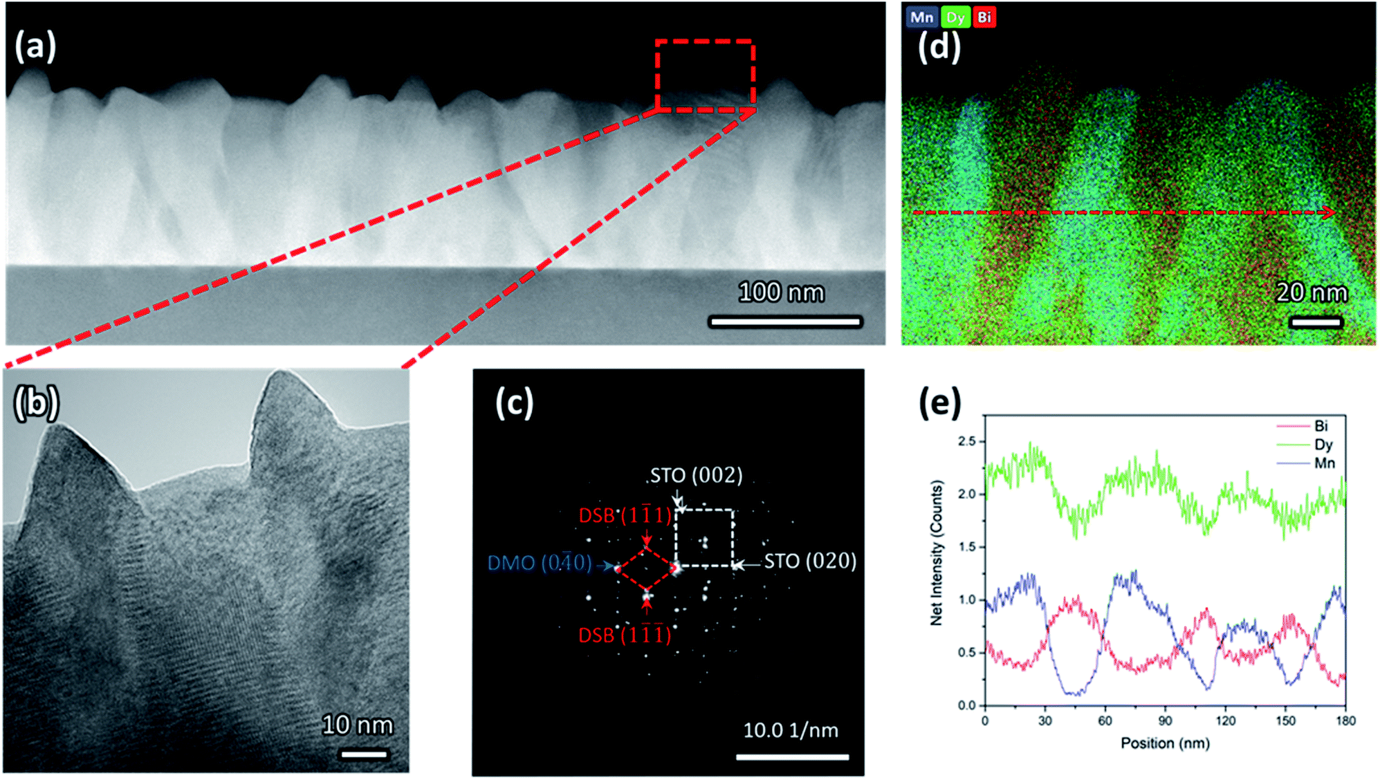 | ||
Fig. 1 (a) Low magnification cross-sectional HAADF-STEM shows clear columnar features that are uniformly distributed (b) high resolution TEM displaying DSB nanopillars which protrude the film surface with pyramidal (111) termination. (c) SAED pattern in STO [001] zone axis indexed to (2![[2 with combining macron]](https://www.rsc.org/images/entities/char_0032_0304.gif) 0)DSB//(020)STO and [110]DSB//[100] STO. (d) EDS map and (e) the corresponding line scan showing clear separation between DSB and DMO phases. Bi (red) and Mn (blue) are localised, whereas Dy (green) is distributed throughout the structure. 0)DSB//(020)STO and [110]DSB//[100] STO. (d) EDS map and (e) the corresponding line scan showing clear separation between DSB and DMO phases. Bi (red) and Mn (blue) are localised, whereas Dy (green) is distributed throughout the structure. | ||
The DSB forms nanopillars (red, Fig. 1d) of ∼30 nm diameter and they are uniformly distributed throughout a DMO matrix (blue, Fig. 1d). The DSB columns protrude the surface of a very dense film (Fig. 1b), with pyramidal faceting indicating (111) termination. The phase boundaries between the two phases are very clean (Fig. 1b), i.e. no secondary phases are present, which is expected since VAN structures form by thermodynamic self-assembly. STEM and EDS confirm our films contain Dy-rich DSB, with a stoichiometry of (Dy2O3)0.6±0.1(Bi2O3)0.4±0.1 (determined from 4 regions), with a minor Mn content (2 ± 0.7% atomic fraction). The high Dy content in the Bi2O3 is expected due to the high Dy content in the target. The DMO has a stoichiometry of Dy0.9±0.1Mn1.00±0.03Bi0.16±0.02O3±δ.
The film orientation and lattice parameters were studied by high resolution XRD (Fig. 2). Symmetric 2θ–ω scans (Fig. 2a) are indexed to a (00l) oriented cubic phase with a = 5.418(2) Å, which is well matched to the Dy stabilised δ-Bi2O3 phase.1 A weak reflection at 28.51° ± 0.05° is indexed to a very minor fraction of (111) DSB. From φ-scans (Fig. 2b), we confirm that the DSB phase is highly aligned and in-plane rotated 45° with an epitaxial relationship of [100]DSB//[110]STO. This is expected as aDSB ≈ √2aSTO. By extension, DMO epitaxially aligns with DSB with the same 45° relationship, as seen in other REMnO3 phases.21–23 This is also expected as DMO has the GdFeO3 perovskite structure.
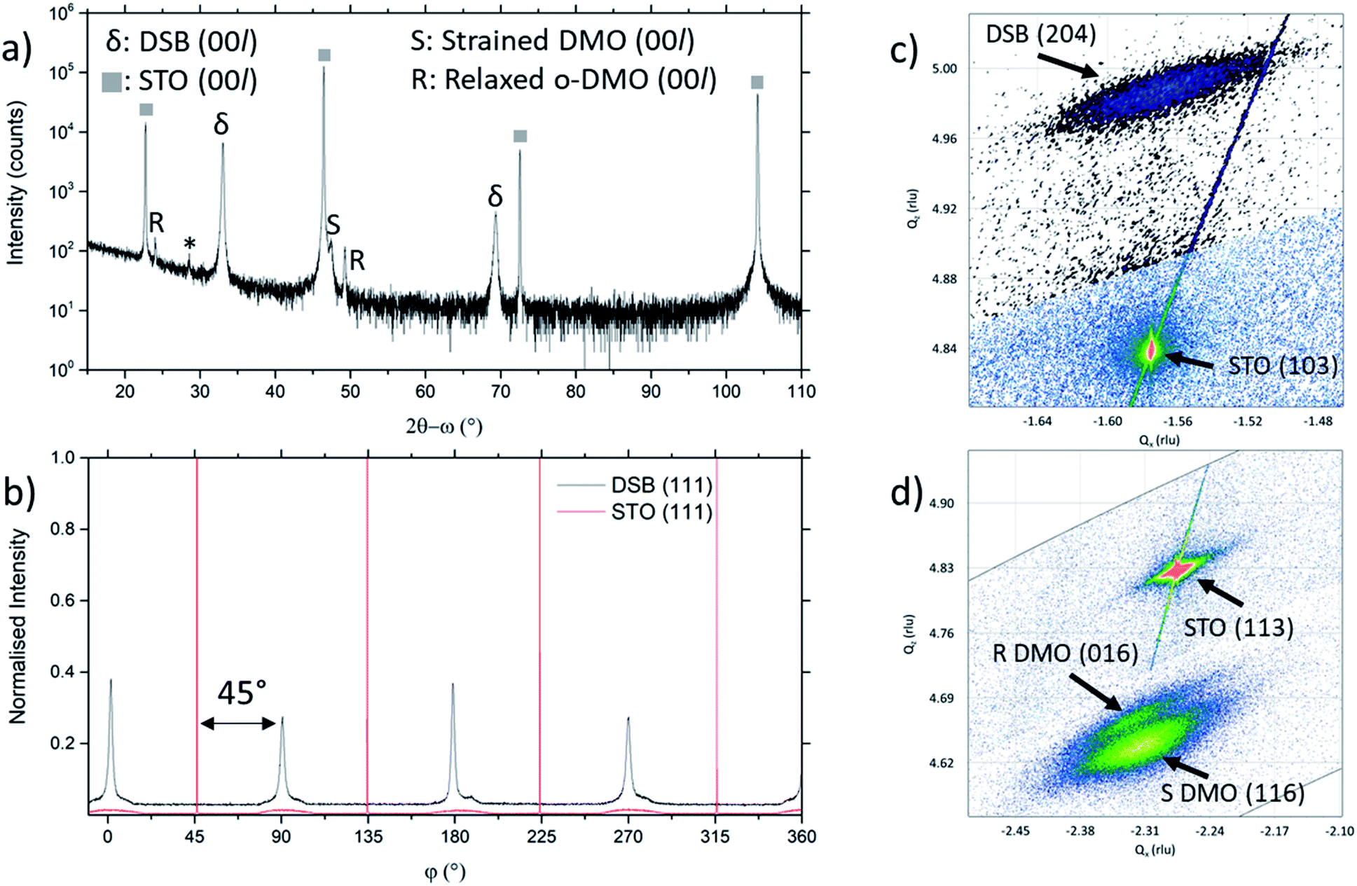 | ||
| Fig. 2 (a) 2θ–ω scans of DSB-DMO VAN films show clear presence of (00l) orientated δ-fluorite DSB and DMO phases. A very small (111) DSB reflection is also present at 28.51° ± 0.05°, marked by * (b) φ scan of (111) STO and DSB reflections, confirming epitaxial relationship between DSB and STO of [100]DSB//[110]STO (c) asymmetric RSM around the STO (103) reflection. The DSB (204) is observed nearby, confirming the fluorite phase (d) asymmetric RSM around the (113) reflection of STO. The (116) reflection of the tetragonally strained DMO is clearly present, alongside the (016) reflection of relaxed DMO. | ||
To further confirm the presence of the cubic δ-fluorite phase, detailed high-resolution asymmetric X-ray reciprocal space maps (RSMs) were collected around the (103) STO reflection (Fig. 2c). This reveals a single broad reflection which is indexed to cubic DSB (204) with a = 5.38(1) Å. Additional evidence that the DSB is indeed the δ fluorite phase of Bi2O3 comes from indexing the SAED pattern in TEM (Fig. 1c). Taken from the STO [100] zone axis, the SAED pattern shows a (20)DSB//(020)STO and [110]DSB//[100]STO orientation relationship, consistent with XRD φ-scans (Fig. 2b), and is indexed with a = 5.452(5) Å, congruent with stabilised δ-Bi2O3.1 Non-indexed SAED spots arise from DMO. The cannot be indexed to the other known phases of Bi2O3 (see Fig. S1† for discussion). Hence, these observations taken together are conclusive proof that cubic DSB can be grown epitaxially in VAN films grown on STO substrates.
We now consider the role of the DMO. The DMO forms mainly as a highly strained phase in the VAN film. This is seen from 2θ–ω XRD scans (Fig. 2a), which shows two reflections to the right of the (002) STO, corresponding to the strained (S) and relaxed (R) DMO phase. The reflection labelled S at lower 2θ arises from DMO (a = 5.280 Å, b = 5.832 Å, c = 7.381 Å)24 which is compressed in-plane by STO (bulk average pseudo-cubic lattice parameter of DMO is 3.932 Å vs. STO 3.905 Å) resulting in a 3.64% out-of-plane tensile strain with c = 7.650(5) Å, as indexed. The VAN structure enables the high strain levels, much higher than standard epitaxial thin films.25,26 An additional reflection observed at higher 2θ, labelled R, indexed to c = 7.393(5) Å corresponds to relaxed DMO which adopts the bulk lattice parameters. This relaxation occurs at the upper part of the film away from the substrate and is minor contribution.
To understand more about the DMO phase, detailed high-resolution asymmetric X-ray reciprocal space maps (RSMs) around the (113) reflection of STO were performed (Fig. 2d). Two broad reflections are witnessed in close proximity to STO (113). We note that both reflections show greater in-plane (Qx) broadening than out-of-plane (Qz). This is related to thermal contraction effects particular to VAN films,25 and is not relevant to the uniform out-of-plane straining, which is the key factor for controlling the stabilisation of the δ-phase of DSB. The larger reflection can be indexed to a tetragonal phase with lattice parameters of a = b = 5.528(5) Å, c = 7.650(5) Å, and is assigned as the (116) reflection of the strained DMO phase as seen in the 2θ–ω scans (Fig. 2a). This confirms that the DMO strains from an orthorhombic to tetragonal unit cell with a 0.63% tensile strain in the [110] direction. We note the significance of 5.52 Å, as it is equal to  indicating that DMO is in-plane straining to perfectly match the [110]STO direction. A second broad reflection is observed which corresponds to the (016) of the relaxed DMO, and can be indexed with b = 5.837(5) Å, c = 7.393(5) Å, thus consistent with the bulk DMO.24 These observations are similar to previously reported (SmMnO3)0.5((Bi,Sm)2O3)0.5 VAN films.21
In our film, the DMO matrix plays an important role in stabilising the cubic DSB phase; the strained DMO and DSB have a ∼2% lattice mismatch. Thus, the strained DMO matrix acts as scaffold to stabilise and promote the formation of cubic DSB nanopillars. Here, vertical strain is induced by the DMO matrix on the DSB pillars in the VAN architecture, enabling stabilisation of the δ-fluorite phase throughout the thickness of the VAN film. Thus, strain relaxation is controlled when confined within VAN, unlike standard planar films where strain is localised to a ∼20 nm region at the film/substrate interface resulting in relaxation as the film thickness.11 In fact, vertical strain stabilisation in VAN can enable stabilisation to micron thick films.27 This should enable the growth of robust, thick films of the δ-phase, >50× thicker than previous superlattice films.12,13
We now discuss the excellent ionic properties of our DSB-DMO VAN films grown on electronically conducting Nb-STO. The out-of-plane ionic conductivity of the DSB-DMO VAN films was studied with EIS, presented in Fig. 3. Nyquist plots, a typical example of which is presented in Fig. 3b, display two features that can be modelled with a Randles circuit (Fig. 3b inset); a small arc at high frequency corresponding to the ionic conductivity of the DSB, modelled by Ri and Ci; and a finite length Warburg (FLW) response appearing as a 45° line at higher frequencies before transitioning into a semi-circle at low frequencies. This FLW response models the complex impedance arising from the diffusion of oxide ions at the electrode interface. From Fig. 3a, it is clearly observed that the ionic conductivity of the DSB-DMO VAN is thermally activated and obeys Arrhenius behaviour with an activation energy of 1.00 ± 0.02 eV, reaching 10−3 S cm−1 at 500 °C. These values are well matched with bulk DSB (1.05–1.12 eV)5 and comparable with erbium stabilised δ-Bi2O3 superlattices (1.05 eV MgO/CGO/[ESB/CGO]N=1, 1.18 eV MgO/CGO/[ESB/CGO]N=20).12 The high ionic conductivity again confirms the presence of the δ-fluorite structure in our VAN films. The ionic conductivity values are moderately lower (3 − 8x) at 500 °C (1.0 × 10⁻³ S cm−1 our film) than previously reported for Er-doped superlattice films (3.3 × 10⁻³ S cm−1 MgO/CGO/[ESB/CGO]N=1, 8.1 × 10⁻³ S cm−1 MgO/CGO/[ESB/CGO]N=20).12,13 However, is important to note that the magnitude of ionic conductivity in doped δ-Bi2O3 decreases with increasing dopant concentration,1,2,5 and our dopant concentrations are higher than reported superlattice films (x = 0.6 cf. nominally x = 0.2 (Er) in [ESB/Ce0.8Gd0.2O2−δ]N,12x = 0 in [δ-Bi2O3/YSZ]N but with possible yttrium intermixing13). As can be seen from Fig. 3a, the ionic conductivity of our films is at a value that is consistent with bulk (Dy2O3)x(Bi2O3)1−x with x ≈ 0.40.5 Since, from EDS maps (Fig. 1e), our x = 0.6 ± 0.1, this indicates the VAN structure has enhanced ionic conduction compared to bulk material of this same composition5 by a factor of ∼50× at 500 °C. This could result from either the enhanced crystallinity of the DSB in the film, and/or possible nano-structuring effects.14,28
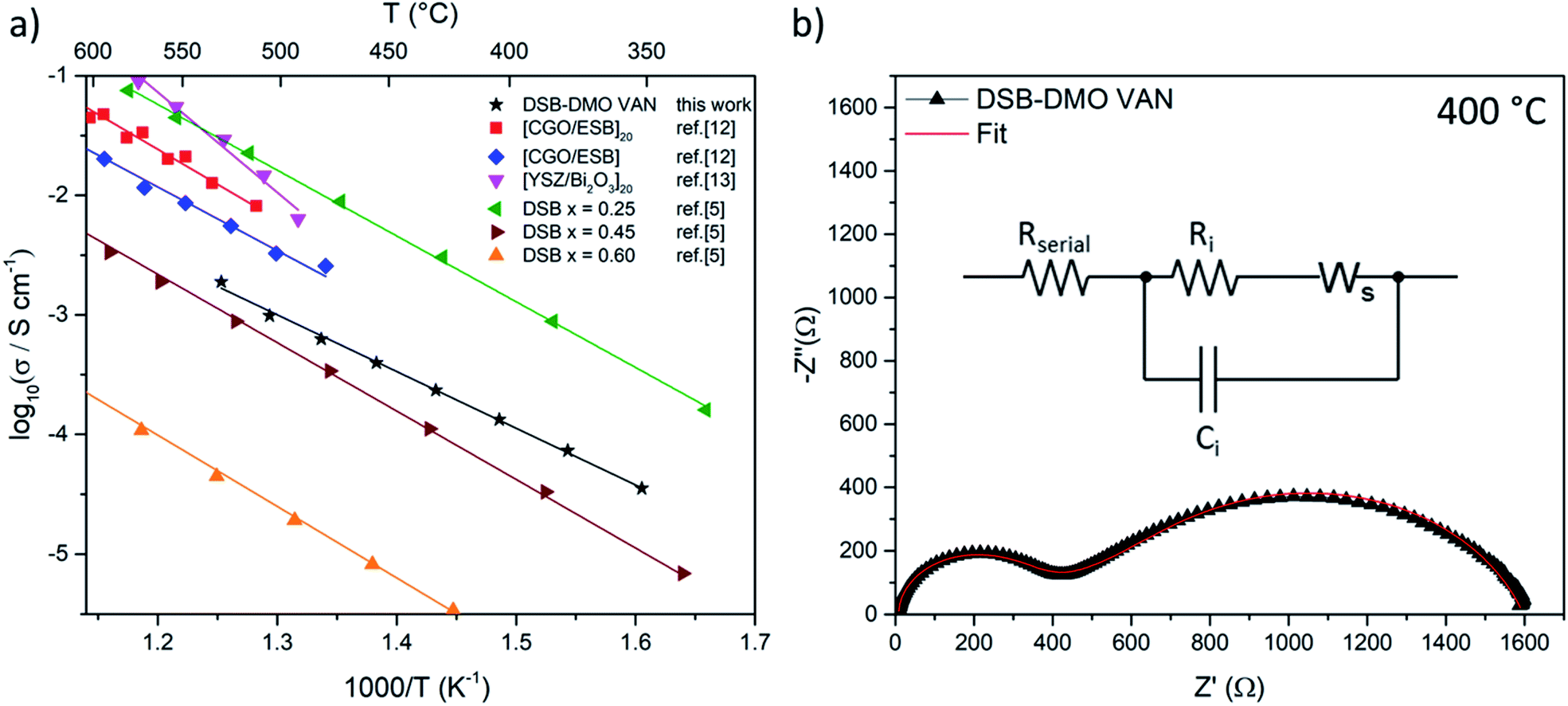 | ||
| Fig. 3 (a) Arrhenius plot of DSB-DMO VAN film in air displaying high ionic conductivity as compared to the literature results for superlattices12,13 and bulk powder DSB5 (b) typical Nyquist plot at 400 °C. Inset; the Randles model used to fit the data, where Ri/Ci models the ionic conductivity of DSB, Ws the FLW response, and Rserial the internal resistances of the EIS setup. | ||
It may be possible to further enhance the ionic conductivity of our films by fine tuning the excess Bi2O3 content such that the Bi:dopant ratio is smaller, hence accessing higher conductivities. Alternatively, different stabilising matrixes could be utilised, or different volume fractions of the matrix/column in the VAN, leading to different strain levels in the δ-Bi2O3, which may further enhance the ionic conductivity.29,30
We note that bulk DMO displays electronic conductivity, with an Ea of 0.268 eV and conductivity greater than 10−1 S cm−1 above 320 °C,31 distinctly different from the observed EIS feature (Fig. 3). To further affirm we are not measuring the EIS of DMO in Fig. 3, we present the EIS of a reference Ag/Nb-STO/DMO/Pt system in Fig. S2.† By comparison, it is clearly seen that the impedance of the DMO planar system is very different to the DSB-DMO VAN. Thus, we conclude the EIS of our VAN system is dominated by DSB. But, from the microstructure in Fig. 1a, there may be a very thin layer of DMO between the DSB column and Nb-STO substrate. In the context of our electrode setup, the DMO acts as an extension of the electrode, and its impedance contribution is contained within Rserial (which also contains contributions from the Nb-STO substrate and the internal resistances of the EIS setup). As the electronic conductivity of DMO would yield a resistance ∼100× smaller than Rserial, it is expected that this feature cannot be deconvoluted from Rserial.
In fact, electronic conductivity in the matrix phase is beneficial, as the system could instead be used as a cathode in thin film μSOFCs. Hence, a VAN film comprised of doped δ-Bi2O3 paired with an electronic conducting matrix could be used. Indeed, erbium stabilised δ-Bi2O3–La1−xSrxMnO3 (LSM) composite cathodes have been gaining interest in bulk powder SOFCs, pairing the superb ionic conductivity of the fluorite δ-Bi2O3 with the high electronic and cathodic performance of LSM, resulting in low areal surface resistances.24–26,32–34 We also draw attention to analogous VAN nanocomposite structures recently reported utilising the same electronic–ionic pairing philosophy.18 Hence, the DSB-DMO VAN reported here could serve as a precursor to a δ-Bi2O3 based VAN cathodes. Alternatively, with an appropriate insulating strain-stabilising matrix phase, it may be possible to yield robust δ-Bi2O3 film electrolytes, and hence form a complete thin μSOFC film cell, e.g. comprised of an epitaxial substrate anode (e.g. Ni-YSZ) on either Si35 or metal36 with two VAN layers above the anode layer, first a δ-Bi2O3-based VAN electrolyte and followed by a δ-Bi2O3 based VAN cathode. Such double VAN ionic structures are readily possible.14
Conclusions
We have shown that it is possible to grow the high ionic conducting fluorite δ-phase of Bi2O3 confined within epitaxial DSB-DMO vertically aligned nanocomposite (VAN) thin films. First, we demonstrated by TEM/STEM and XRD that DSB grows epitaxially with the cubic fluorite structure. Thereafter, we showed the ionic conductivity of the DSB phase reaches 10−3 S cm−1 at 500 °C, comparable with previously reported superlattice films, but with important advantages for building practical devices, first that the ion channels are in the required out-of-plane direction and second that VAN films do not impose severe film thickness limitations. Our work marks an important advance towards the development of highly conductive δ-Bi2O3 based cathodes and electrolytes for μSOFCs for portable power applications.Author contributions
The manuscript was written through contributions of all authors. All authors have given approval to the final version of the manuscript. JLM-D and AJL conceived the idea. AJL wrote the draft of the manuscript before others contributed. Samples were grown by MPW; XRD and EIS measurements were conducted by AJL; TEM and EDS was performed by HW, JL and ZH.Conflicts of interest
There are no conflicts to declare.Acknowledgements
The acknowledgements come at the end of an article after the conclusions and before the notes and references. JLM-D acknowledges support from the Royal Academy of Engineering Chair in Emerging Technologies, grant CIET1819_24. JLM-D and MPW acknowledge support from the EPSRC Centre of Advanced Materials for Integrated Energy Systems (CAM-IES) under EP/P007767/1 and European Union's Horizon 2020 research and innovation programme under grant agreement no. 10101017709 (Epistore). AJL acknowledges support from the EPSRC (EP/R513180/1). ZH, JL and HW acknowledge the support from the US National Science Foundation for the TEM work performed at Purdue University (DMR-2016453 and DMR-1809520).References
- N. Jiang and E. D. Wachsman, J. Am. Ceram. Soc., 1999, 82, 3057–3064 CrossRef CAS.
- N. M. Sammes, G. A. Tompsett, H. Näfe and F. Aldinger, J. Eur. Ceram. Soc., 1999, 19, 1801–1826 CrossRef CAS.
- E. D. Wachsman, S. Boyapati and N. Jiang, Ionics, 2001, 7, 1–6 CrossRef CAS.
- M. J. Verkerk and A. J. Burggraaf, Solid State Ionics, 1981, 3–4, 463–467 CrossRef CAS.
- M. J. Verkerk and A. J. Burggraaf, J. Electrochem. Soc., 1981, 128, 75–81 CrossRef CAS.
- D. W. Jung, K. L. Duncan and E. D. Wachsman, Acta Mater., 2010, 58, 355–363 CrossRef CAS.
- X. Kuang, J. L. Payne, M. R. Johnson and I. E. Radosavljevic, Angew. Chem., Int. Ed., 2012, 51, 690–694 CrossRef CAS PubMed.
- S. Sanna, V. Esposito, C. Graves, J. Hjelm, J. W. Andreasen and N. Pryds, Solid State Ionics, 2014, 266, 13–18 CrossRef CAS.
- S. Kąc, G. Szwachta, Ł. Cieniek and T. Moskalewicz, Arch. Metall. Mater., 2019, 64, 969–974 Search PubMed.
- S. J. Jeong, N. W. Kwak, P. Byeon, S. Y. Chung and W. Jung, ACS Appl. Mater. Interfaces, 2018, 10, 6269–6275 CrossRef CAS PubMed.
- L. S. J. Peng, X. X. Xi, B. H. Moeckly and S. P. Alpay, Appl. Phys. Lett., 2003, 83, 4592–4594 CrossRef CAS.
- S. Sanna, V. Esposito, J. W. Andreasen, J. Hjelm, W. Zhang, T. Kasama, S. B. Simonsen, M. Christensen, S. Linderoth and N. Pryds, Nat. Mater., 2015, 14, 500–504 CrossRef CAS PubMed.
- S. Sanna, V. Esposito, M. Christensen and N. Pryds, APL Mater., 2016, 4, 2–7 Search PubMed.
- S. Lee and J. L. MacManus-Driscoll, APL Mater., 2017, 5, 42304 CrossRef.
- S. Lee, W. Zhang, F. Khatkhatay, H. Wang, Q. Jia and J. L. MacManus-Driscoll, Nano Lett., 2015, 15, 7362–7369 CrossRef PubMed.
- S. M. Yang, S. Lee, J. Jian, W. Zhang, P. Lu, Q. Jia, H. Wang, T. W. Noh, S. V Kalinin and J. L. MacManus-Driscoll, Nat. Commun., 2015, 6, 1–8 CAS.
- J. Yoon, S. Cho, J.-H. Kim, J. Lee, Z. Bi, A. Serquis, X. Zhang, A. Manthiram and H. Wang, Adv. Funct. Mater., 2009, 19, 3868–3873 CrossRef CAS.
- F. Baiutti, F. Chiabrera, M. Acosta, D. Diercks, D. Parfitt, J. Santiso, X. Wang, A. Cavallaro, A. Morata and H. Wang, et al. , Nat. Commun., 2021, 12, 1–11 CrossRef PubMed.
- B. H. Yun, K. J. Kim, D. W. Joh, M. S. Chae, J. J. Lee, D. W. Kim, S. Kang, D. Choi, S. T. Hong and K. T. Lee, J. Mater. Chem. A, 2019, 7, 20558–20566 RSC.
- R. D. Bayliss, S. N. Cook, S. Kotsantonis, R. J. Chater and J. A. Kilner, Adv. Energy Mater., 2014, 4, 2–7 Search PubMed.
- E. M. Choi, T. Maity, A. Kursumovic, P. Lu, Z. Bi, S. Yu, Y. Park, B. Zhu, R. Wu, V. Gopalan, H. Wang and J. L. MacManus-Driscoll, Nat. Commun., 2020, 11, 1–9 Search PubMed.
- X. Martí, F. Sánchez, V. Skumryev, V. Laukhin, C. Ferrater, M. V. García-Cuenca, M. Varela and J. Fontcuberta, Thin Solid Films, 2008, 516, 4899–4907 CrossRef.
- X. Marti, V. Skumryev, C. Ferrater, M. V. García-Cuenca, M. Varela, F. Sánchez and J. Fontcuberta, Appl. Phys. Lett., 2010, 96, 2008–2011 CrossRef.
- S. Harikrishnan, S. Rößler, C. M. Naveen Kumar, H. L. Bhat, U. K. Rößler, S. Wirth, F. Steglich and S. Elizabeth, J. Phys.: Condens. Matter, 2009, 21(9), 096002 CrossRef CAS PubMed.
- J. MacManus-Driscoll, A. Suwardi, A. Kursumovic, Z. Bi, C. F. Tsai, H. Wang, Q. Jia and O. J. Lee, APL Mater., 2015, 3(6), 062507 CrossRef.
- J. L. MacManus-Driscoll, P. Zerrer, H. Wang, H. Yang, J. Yoon, A. Fouchet, R. Yu, M. G. Blamire and Q. Jia, Nat. Mater., 2008, 7, 314–320 CrossRef CAS PubMed.
- S. A. Harrington, J. Zhai, S. Denev, V. Gopalan, H. Wang, Z. Bi, S. A. T. Redfern, S. H. Baek, C. W. Bark, C. B. Eom, Q. Jia, M. E. Vickers and J. L. MacManus-Driscoll, Nat. Nanotechnol., 2011, 6, 491–495 CrossRef CAS PubMed.
- J. Maier, Nat. Mater., 2005, 4, 805–815 CrossRef CAS PubMed.
- S. Lee, W. Zhang, F. Khatkhatay, Q. Jia, H. Wang and J. L. Macmanus-Driscoll, Adv. Funct. Mater., 2015, 25, 4328–4333 CrossRef CAS.
- J. Huang, J. L. MacManus-Driscoll and H. Wang, J. Mater. Res., 2017, 32, 4054–4066 CrossRef CAS.
- B. Dabrowski, S. Kolesnik, A. Baszczuk, O. Chmaissem, T. Maxwell and J. Mais, J. Solid State Chem., 2005, 178, 629–637 CrossRef CAS.
- J. Zamudio-García, N. Albarrán-Aroca, J. M. Porras-Vázquez, E. R. Losilla and D. Marrero-López, Appl. Nano, 2020, 1(1), 14–24 CrossRef.
- A. S. Painter, Y. L. Huang and E. D. Wachsman, J. Power Sources, 2017, 360, 391–398 CrossRef CAS.
- K. T. Lee, D. W. Jung, H. S. Yoon, M. Camaratta, N. Sexson and E. D. Wachsman, ECS Trans., 2011, 35, 1861–1869 CrossRef CAS.
- A. Evans, A. Bieberle-Hütter, J. L. M. Rupp and L. J. Gauckler, J. Power Sources, 2009, 194, 119–129 CrossRef CAS.
- M. P. Wells, A. J. Lovett, T. Chalklen, F. Baiutti, A. Tarancón, X. Wang, J. Ding, H. Wang, S. Kar-Narayan, M. Acosta and J. L. Macmanus-Driscoll, ACS Appl. Mater. Interfaces, 2021, 13, 4117–4125 CrossRef CAS PubMed.
Footnote |
| † Electronic supplementary information (ESI) available. See DOI: 10.1039/d1ta07308g |
| This journal is © The Royal Society of Chemistry 2022 |