
Flexible electronics based on 2D transition metal dichalcogenides
Dongting
Jiang
a,
Zhiyuan
Liu
 b,
Zhe
Xiao
a,
Zhengfang
Qian
a,
Yiling
Sun
a,
Zhiyuan
Zeng
c and
Renheng
Wang
*a
b,
Zhe
Xiao
a,
Zhengfang
Qian
a,
Yiling
Sun
a,
Zhiyuan
Zeng
c and
Renheng
Wang
*a
aKey Laboratory of Optoelectronic Devices and Systems of Ministry of Education and Guangdong Province, College of Physics and Optoelectronic Engineering, Shenzhen University, Shenzhen 518060, China
bShenzhen Institutes of Advanced Technology, Chinese Academy of Sciences, Shenzhen 518055, China
cDepartment of Materials Science and Engineering, City University of Hong Kong, Hong Kong 999077, China
First published on 15th November 2021
Abstract
Flexible devices play an important role in various fields such as electronics, industry, healthcare, military, space exploration, and so on. Traditional materials used for flexible devices include silicon, inorganic oxides, and polymers. However, these materials show some drawbacks such as high rigidity, low electrical conductivity, or being costly for large-scale manufacturing. Transition metal dichalcogenides (TMDs) have attracted great interest in the last decade due to their layered structures, and relevant publications have gained rapid growth. TMDs exhibit tunable properties as a function of layers. TMDs show semiconducting/metallic transition, direct/indirect band transition, strengthened flexibility, and increased transparency with the decreasing layer number. Such tunable properties of TMDs allow them to be promising materials for flexible devices. As part of this review, the initial discussion is on the structural information of TMDs. Subsequently, recent improved synthetic routes and phase engineering of TMDs will be introduced. Then, we introduce the studies and challenges of flexible and stretchable devices. And then we review some recent studies on TMD-based flexible devices, including transistors, energy storage devices, and sensors. In the end, some comprehensive discussion and perspectives for the future trend of flexible devices will be given.
 Dongting Jiang | Dr Dongting Jiang received his Ph.D. degree in Ceramics and Glasses from the University of Manchester (UOM) in 2019. He is currently a postdoctoral researcher at the College of Physics and Optoelectronic Engineering, Shenzhen University. His research focuses on the synthesis and applications of thermoelectric materials, advanced material processing techniques, and flexible energy devices. |
 Zhe Xiao | Zhe Xiao is a PhD student in the School of Physics and Opto-electronic Engineering, Shenzhen University (SZU). His research interests include lithium-ion batteries, two-dimensional nanomaterials, and devices. He has co-authored many journal articles and participated in two domestic academic conferences. |
 Zhengfang Qian | Dr Zhengfang Qian obtained his PhD degree from Chongqing University in 1991. Since 2016, he has been a Chair Professor in Shenzhen University. His current research interests include nanostructured antennas, sensors, devices, and batteries. |
 Yiling Sun | Prof. Yiling Sun received her Ph.D. degree in Electronic Science and Technology from Zhejiang University in 2005. She worked as a lecturer and later as Associate Professor at Shenzhen University from 1997 to 2007. She was an Associate Professor and then Professor at China Jiliang University from 2007 to 2010. In 2011, she rejoined the faculty of Shenzhen University, where she is currently a Professor at the College of Physics and Optoelectronic Engineering. Her current research interests include integrated optical devices and their applications. |
 Renheng Wang | Dr Renheng Wang received his Ph.D. degree in Metallurgical Engineering from Central South University (CSU) in 2015. From January 2016 to October 2018, he worked as a postdoctoral follow at Shenzhen University and Nanyang Technological University. He is currently an Assistant Professor at the College of Physics and Optoelectronic Engineering, Shenzhen University. His research focuses on the synthesis and application of nanomaterials and composites for flexible devices, energy conversion and storage, such as high-power/high-energy lithium-ion batteries. |
1. Introduction
For decades, the development of flexible electronics kept growing while research studies of 2D materials have accelerated the rapid development of flexible devices. Due to flexibility, devices can accommodate bending and stretching, and be adapted into various applications, such as bendable smartphone screens, nano-size electronic transistors,1–5 large-area electronic paper,6–8 energy devices,9–11 wearable biosensors,12etc. The realization of a flexible electronic device with high performance strongly depends on the materials that are chosen. The development of flexible electronic materials has had a long history as everything can be flexible if thin enough. A timetable revealing the historical development of flexible materials and their specific applications is shown in Fig. 1. Early in the 1960s, people fabricated the first flexible solar cells using single crystal silicon to deposit on plastic substrates.13 Since then, other conventional flexible materials emerged, such as amorphous silicon, transition metal oxides, polymers, and organic materials.14 However, these materials either exhibit relatively poor electrical properties or are costly.15 Since the 2000s, the development of 2D materials has opened new avenues for flexible electronics. These advanced 2D materials exhibit interesting electrical behaviors and high flexibility owing to the 2D feature. Among them, TMDs attracted intensive research interest due to their unique features. The in-layer atoms are covalently bonded, and each layer is attached by van der Waals (vdW) forces. Therefore, a TMD monolayer can be easily exfoliated off and attached on different substrates. The combination of M and X brings great variation in the electrical, mechanical, and optical properties of TMDs.16–19 Besides, the tunable physical properties of TMDs show great dependence on the thickness.20 The electrical performance of TMDs relies on the filling state of the d orbitals of the transition metals. Low dimensional TMDs exhibit weakened interactions between interlayers, leading to an opening of the bandgap of TMDs as well as metallic/semiconducting transition. Some TMDs also show an indirect/direct bandgap transition when the material dimension is 2D, which leads to a thickness-dependent photoelectric behavior. In terms of the mechanical properties, monolayer and few-layer TMDs show a Young's modulus of about 200 GPa,19 which is greater than that of most of the state-of-the-art 2D materials.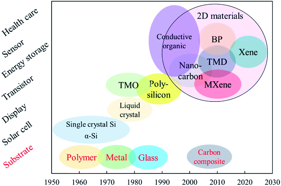 | ||
| Fig. 1 The milestone of materials for flexible electronics. | ||
To further improve the device flexibility, TMD circuits can be integrated on a standard substrate first, and then transferred onto an elastic platform, such as a polymer sheet or metal foil.21–23 However, such a method is usually costly and yields small surface area coverage.24 Hence, multiple innovative process techniques have been developed for TMD materials, which aim at the precise synthesis, minimizing damages, transferring large-area films, and realizing polycrystalline or amorphous semiconductors.25–28 In addition, TMDs are adaptable for advanced device architecture,29–31 which can further enhance the device flexibility and stretchability. Such device configurations include the “island and bridge” design where the stretching stress is divided and the majority is carried by flexible wires,32 the “wavy” geometry where the pre-strained substrate can bear bending and rolling along the wave direction,33,34 the fiber cloth which is flexible, comfortable, lightweight, and suitable for wearable electronics with a large cover area,35,36 and the “honeycomb” geometry that takes advantage of high stretchability and large specific area.37–39
Due to these superior properties, TMDs have been utilized for different flexible applications. A timetable is shown in Fig. 2 presenting the milestones in the historical evolution of TMD-based flexible and wearable electronics. The first TMD-based thin film transistor (TFT) was fabricated around 2004, promoting the rapid development of flexible electronics based on TMDs.40 It only took a few years for the realization of flexible energy storage devices, photodetectors, LEDs, memories, actuators, etc.41–46 TMDs have also been used in energy fields. Since the 2010s, TMD-based flexible solar cells, lithium-ion batteries (LIBs), thermoelectric generators (TEGs), etc. have been realized successively.47–50 During the last five years, applications of TMD electronics in human health care and biotherapy were rapidly explored. E-skin and wearable biosensors have gained growing popularity, which aim at the detection of body movements, toxic gases, bio-signals, etc.51–55 Nowadays, the growing popularity of 5G communication techniques accelerates the research studies into flexible antennas. Palacios' group56 has successfully realized the MoS2-based rectenna that can convert electromagnetic waves into direct current, which opened avenues for new flexible TMD-based applications.
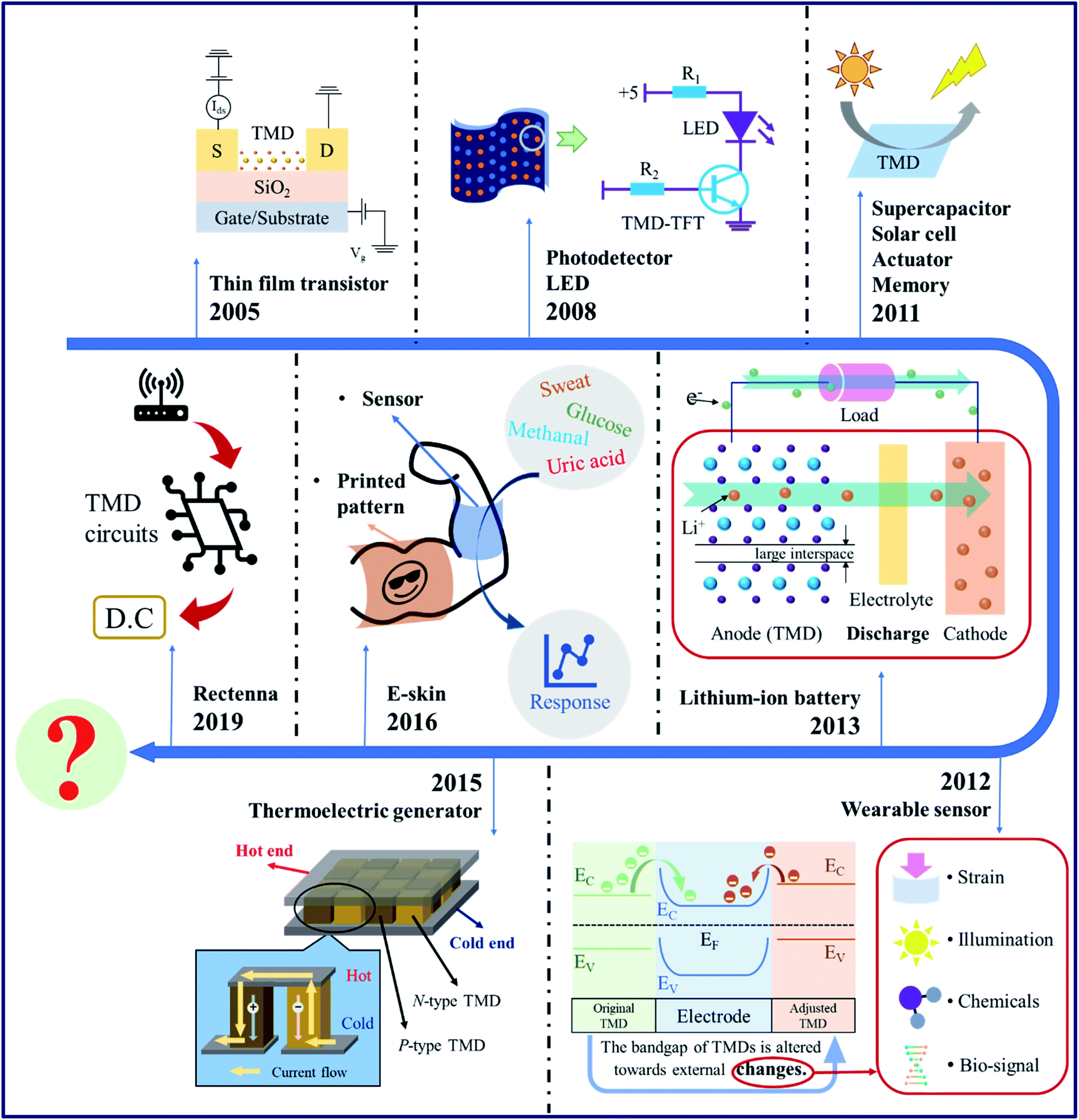 | ||
| Fig. 2 The timeline of some key TMD-based flexible electronics. | ||
Herein, as part of this study, we revolve around the recent work of flexible and wearable devices based on TMD materials. Firstly, a brief introduction to the features of TMDs as well as the crystal structure and physical properties will be given, and a short comparison of different 2D materials will be clarified. Secondly, synthetic approaches to TMD materials are discussed, which builds a fundamental understanding of how TMDs are integrated into flexible devices. Finally, we summarize and discuss some recent studies of flexible electronics based on TMDs. The outline of this paper is illustrated by a schematic graph in Fig. 3.
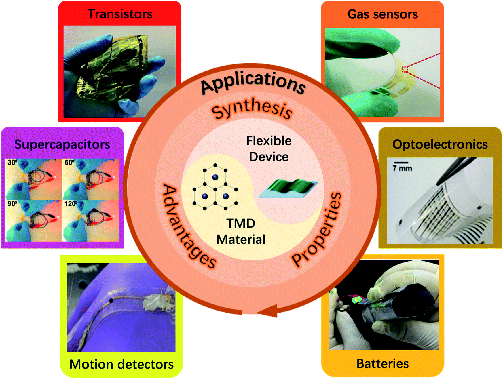 | ||
| Fig. 3 The scheme showing of the general topics in this review paper. Reproduced with permission from ref. 57, copyright 2018 Advanced Functional Materials; ref. 58, copyright 2019 Nano Energy; ref. 59, copyright 2018 Science Advances; ref. 60, copyright 2019 Chemical Engineering Journal; ref. 61, copyright 2020 Nanotechnology; ref. 62, copyright 2018 Journal of Materials Chemistry A. | ||
2. Flexible electronics
2.1. 2D materials towards flexible electronics
Flexible electronics refer to those with bendability, rollability, and/or foldability.63 Generally, flexible electronics refer to the integration of functioning electronic circuits (the frontplane) and the controlling transistors (the backplane) on a flexible substrate. For the frontplane and backplane, semiconductors with superior photoelectric, chemoelectric, or mechanical properties are favorable. Traditional bulk semiconducting materials such as silicon and transition metal oxides (TMOs) show outstanding electrical behaviors, but their poor mechanical flexibility limits their applications in flexible areas.64–67 In 2004, the discovery of graphene by Andre Geim and Kostya Novoselov68 opened the gate to the rapid development of 2D materials. Such materials include 2D mono-elemental materials, transition metal chalcogenides (TMCs), transition metal dichalcogenides (TMDs), transition metal carbides and nitrides (MXenes), etc. Owing to their small scales down to the nano-level, these materials exhibit superior electrical properties and mechanical strength compared to their bulk states, which satisfy the criteria for the construction of flexible devices.69 Hence, 2D materials push the development of flexible electronics by a huge step.Carbon nanotubes (CNTs) are typical 1D materials with intrinsic high electrical conductivity and flexibility. They are widely used to serve as building blocks for flexible electronics, such as supercapacitors and transparent electrodes.70–72 Their large aspect ratios lead to high optical transmittance. Therefore, they can be assembled into a porous and transparent network with high conductivity and flexibility. CNT electronics can be fabricated at room temperature by conventional spin coating or spraying methods. However, CNTs agglomerate in solution due to their strong internal vdW forces. Hence surfactants and organics are employed to stabilize CNTs under aqueous conditions.73,74 Graphene is a typical 2D material with remarkable physical and chemical performances and has been studied for decades.75 It displays a high carrier field-effect mobility reaching ∼104 cm2 V s−1 and withstands bending and stretching. However, the zero bandgap leads to current leakage when used as active materials. Graphene oxide (GO) is formed with the oxidation of graphene, which consists of G–O bonds in sp3 hybridization. As the G–G bonds are sp2 hybridized, the presence of O introduces disorder and alters the crosslinked network of graphene, opening the bandgap to 10–50 meV.76,77 Oxidation of graphene can be reversed by annealing or chemical reactions, which leads to the formation of reduced graphene oxide (RGO). By gradual removal of oxygen from GO, the material shows the insulating–semiconducting–semi metallic transition.78,79 Therefore, the conductivity of graphene can be controlled with different oxidation/reduction degrees.
Recently, a new term Xene arose, which refers to the monolayer of group IIIA–VA elemental crystals. In addition to graphene, Xenes also include phosphorene (black phosphorus monolayer), borophene, arsenene, antimonene, bismuthene, tellurene, etc. Black phosphorus (BP) is a layer-structured 2D material with each layer bonded via vdW forces. In each layer, one phosphorus atom is covalently bonded to three adjoining phosphorus atoms in sp3 hybridization, which allows monolayered BP to present promising flexibility. The electrical properties of BP are anisotropic and tunable with layer numbers. Along the x-direction, monolayer BP presents an electron (hole) mobility of ∼1100 (670–700) cm2 V−1 s−1. However for the y-direction, the value shows a great difference, which is ∼80 (10![[thin space (1/6-em)]](https://www.rsc.org/images/entities/char_2009.gif) 000–26000) cm2 V−1 s−1.80 Besides, the hole mobility in accordance with the x-direction increases from 600 cm2 V−1 s−1 for the monolayer to 4000 cm2 V−1 s−1 for five-layer BP.80 The direct bandgap increases from ∼0.3 eV for the bulk state to 2 eV for the monolayer.81 These unique features allow BP to be used for supercapacitors and electrocatalysts.82–84 Borophene is a new-born 2D material, which has an anisotropic planar structure with corrugation along the a-direction and buckling along the b-direction.85 The boron atoms exhibit stable sp3 hybridization, which is responsible for buckling along the b-direction.86 The computational work predicated that borophene presents metallic behavior along the a-direction, but semiconductor along the b-direction with a bandgap in the range of 4.43–9.66 eV or 6.45–11.22 eV according to the different calculations.85 The carrier mobility of borophene is comparable to that of graphene, which reaches 105 cm2 V−1 s−1, and 50% of the value can be maintained at a high doping concentration of 1012 cm−2.87 Borophene also exhibits anisotropic mechanical behaviors along the a- and b-directions,88 as the anisotropic Young's modulus is 389 GPa nm and 166 GPa nm, respectively.89 It is highlighted that the height of buckling is a significant factor that enhances the flexibility of borophene along the b-direction. Therefore, the critical strain is 0.08 and 0.15 along the a- and b-directions, respectively. As a result, the biaxial Young's modulus and critical strain for borophene are 250 GPa nm and 0.15, respectively.
000–26000) cm2 V−1 s−1.80 Besides, the hole mobility in accordance with the x-direction increases from 600 cm2 V−1 s−1 for the monolayer to 4000 cm2 V−1 s−1 for five-layer BP.80 The direct bandgap increases from ∼0.3 eV for the bulk state to 2 eV for the monolayer.81 These unique features allow BP to be used for supercapacitors and electrocatalysts.82–84 Borophene is a new-born 2D material, which has an anisotropic planar structure with corrugation along the a-direction and buckling along the b-direction.85 The boron atoms exhibit stable sp3 hybridization, which is responsible for buckling along the b-direction.86 The computational work predicated that borophene presents metallic behavior along the a-direction, but semiconductor along the b-direction with a bandgap in the range of 4.43–9.66 eV or 6.45–11.22 eV according to the different calculations.85 The carrier mobility of borophene is comparable to that of graphene, which reaches 105 cm2 V−1 s−1, and 50% of the value can be maintained at a high doping concentration of 1012 cm−2.87 Borophene also exhibits anisotropic mechanical behaviors along the a- and b-directions,88 as the anisotropic Young's modulus is 389 GPa nm and 166 GPa nm, respectively.89 It is highlighted that the height of buckling is a significant factor that enhances the flexibility of borophene along the b-direction. Therefore, the critical strain is 0.08 and 0.15 along the a- and b-directions, respectively. As a result, the biaxial Young's modulus and critical strain for borophene are 250 GPa nm and 0.15, respectively.
MXenes refer to transition metal carbides and nitrides with layered structures.90 The general formula for MXenes is Mn+1XnTx (n = 1, 2, 3). M, X, and T refer to the transition metals, C or N, and functional groups, respectively. It is reported that all pristine M2X phases exhibit metallic behaviors with zero bandgaps. However most MXenes are semiconductors with a bandgap around 0.24–1.8 eV.91 Their band structures are composed of the transition metal d orbitals as the conduction band and the carbon or nitrogen p orbitals as the valence band. The band structures can be tuned by different functional groups. For example, pure and F-functionalized Ti2C are metallic, while O-functionalized Ti2C is semiconducting due to that O atoms accept electrons and shift the Fermi energy. Like BP, MXenes show anisotropy in electrical properties as well. For example, Ti2CO2 monolayers show an electron (hole) mobility of 6.11 × 10² (7.41 × 10⁴) cm2 V−1 s−1 along the x-direction, and 2.54 × 10² (2.25 × 10⁴) cm2 V−1 s−1 along the y-direction.92 The values are inferior to those of graphene but comparable to those of BP.
2.2. TMD materials: structures, properties, and merits
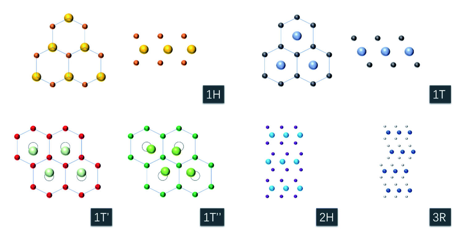 | ||
| Fig. 4 Scheme of the different phases of TMDs. | ||
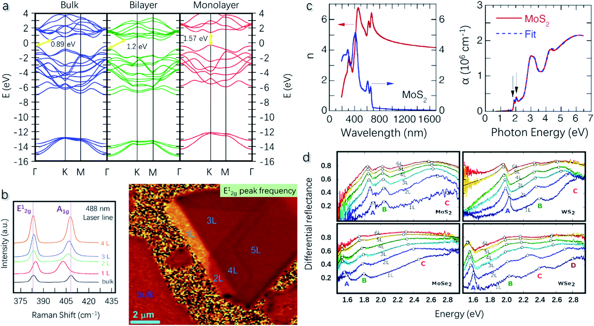 | ||
| Fig. 5 (a) Calculated band structures of bulk, bilayer, and monolayer MoS2. Bulk and bilayer MoS2 show an indirect bandgap of 0.89 and 1.2 eV, respectively. Monolayer MoS2 shows a direct bandgap of 1.57 eV. Reproduced with permission from ref. 96, copyright 2014 Graphene. (b) Raman spectrum of MoS2 with different thicknessess revealing the peak shift of E12g and A1g. The Raman mapping with the E12g peak frequency can identify the layer number of MoS2 flakes from monolayer to bulk. Reproduced with permission from ref. 105, copyright 2012 Advanced Functional Materials. (c) Refractive index, extinction coefficient, and optical absorption coefficient of monolayer MoS2. Reproduced with permission from ref. 18, copyright 2014 Applied Physics Letters. (d) Differential reflectance of MoS2, MoSe2, WS2, and WSe2 as a function of thickness. Reproduced with permission from ref. 114, copyright 2018 Nanomaterials. | ||
Liu et al.18 reported the refractive index, extinction coefficient, and optical absorption coefficient of monolayer MoS2, MoSe2, WS2, and WSe2. MoS2 is taken as an example, whose optical parameters are plotted in Fig. 5c. The material exhibits an anomalously increasing refractive index with the wavelength, but the value reaches a constant of 3.5–4.0 over 800 nm. A maximum value of 4.25 is obtained at 540 nm. The extinction coefficient has a similar trend indicating the strong absorption of near-ultraviolet and visible light. Double peaks around 2 eV can be observed in the optical absorption coefficient spectrum, which correspond to the A/B excitonic absorption peaks. Excitons refer to electron and hole pairs that are in a bound state due to Coulomb attraction. In Mo- and W-based TMDs, excitons influence their optical properties such as light absorption, photoluminescence emission, resonant Raman behavior, etc.107–111 In a typical optical absorption spectrum of MoS2, two characteristic regions with a double-peak structure can be observed, which emerge in the phonon energy ranges of 1.8–2.0 eV and 2.7–3.0 eV, corresponding to the A/B and C/D excitons, respectively.112 For monolayers, A/B exciton pairs arise from the valence band splitting due to the spin-orbital interaction at the K-point in the Brillouin zone. For multilayers, the origin is a combination of spin-orbital and interlayer interactions.113 The C/D excitons are formed due to the multiple optical transitions at the Γ-point.114 The differential reflectance of MoS2 was calculated from the absorption coefficient by Niu et al.114 The data are shown in Fig. 5d, which turns out to be a function of thickness. A red-shift can be observed for the A and C excitons with the increasing layer number, while the peaks for B excitons remain unchanged. This can be explained by the indirect–direct bandgap transition at the K-point in the Brillouin zone as aforementioned.101,115 MoSe2, WS2, and WSe2 show a similar peak shift in the optical spectra. Besides, WSe2 shows an additional signal from D excitons, which is attributed to the transition of the spin-split valence band to the lowest conduction band.114
Compared to MoS2, other MoX2 and WX2 present analogous mechanical properties by virtue of their comparable structure and bond length. As reported, the estimated Young's modulus for MoSe2, WSe2, and WS2 monolayers is in the range of 171.4–218.8 GPa.19 In another case, the biaxial Young's modulus for MoX2 and WX2 is in the range of 154.5–291.2 GPa.126 The compositional difference in the Young's modulus for TMDs is attributed to the overlap of the d orbitals of transition metal atoms and p orbitals of X atoms leading to strong hybridization. The d–p hybridization with deeper d bands below the Fermi level results in a stronger M–X bond.126 Therefore, W-based TMDs are stronger than Mo-based TMDs and sulfides are stronger than the selenides and tellurides. MoX2 and WX2 TMD monolayers show strong mechanical anisotropy, as a higher E value is achieved in the armchair direction over the zigzag direction. Besides, the tensile strain potentially reduces the Young's modulus, as the atomic separation increases upon stretching, which reduces the bonding force.19
Due to the superior strength of TMDs, strain engineering is applied to these materials. Tensile strain is suggested to reduce the bandgap of TMDs and induce a direct–indirect semiconductor transition.19,127–130 The strain brings changes in the charge localization and effective mass of electrons and holes. It also alters the valence and conduction band edges in lower states at the Brillouin zone K-point.127,131,132 In addition to the band structure, the dielectric constants of MoX2 and WX2 can be significantly affected by isotropic strains.133 Strain-induced changes in magnetic properties were also reported for monolayer TMDs.134–136 Strain is also expected to adjust the optical performance of TMDs, which is related to their band structures. In WS2/MoS2 heterostructures, uniaxial strain results in a reduction of the bandgap, which leads to a redshift with rates of 53 and 62 meV %strain−1 for neutral and charged exciton peaks, respectively.137 Lee et al.138 further investigated the influence of tensile strain on the optoelectronic properties of MoX2/WX2 heterostructures. The power conversion efficiency can be improved by 15–35% with a uniaxial tensile strain of 4%. These results indicate the potential of strain engineering as a strategy to strengthen the electrical and optoelectronic performance of TMD-rooted flexible apparatus.
In conclusion, most TMDs show semiconducting behaviors with a large bandgap in the ambient environment. By reducing the layer number, semiconducting/metallic, and indirect/direct bandgap transitions can be induced. Also, the optical absorption spectrum shows dependency on the TMD thickness, indicating that TMDs can be integrated into electronic and optical devices. On the other hand, TMDs show high tolerance to mechanical deformation, and their mechanical strength can be further enhanced by controlling the layer number. This indicates their potential in flexible devices. Moreover, it is suggested that strain can cause changes in the bandgap and optoelectronic properties of TMDs, which allows these materials to be promising candidates for motion detection devices or sensors.
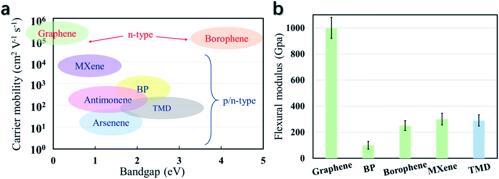 | ||
| Fig. 6 The carrier mobility, bandgap (a), and flexural modulus (b) of some state-of-the-art 2D materials, revealing the potential of TMDs for flexible electronic applications. | ||
In conclusion, most TMDs show semiconducting behaviors with a large bandgap in the ambient environment. By reducing the layer number, semiconducting/metallic, and indirect/direct bandgap transitions can be induced. Besides, the optical absorption spectrum also shows dependency on the TMD thickness, indicating that TMDs can be integrated into electronic and optical devices. On the other hand, TMDs show high tolerance to mechanical deformation, and their mechanical strength can be further enhanced by controlling the layer number. Moreover, it is suggested that strain can cause changes in the bandgap and optoelectronic properties of TMDs, which is feasible for motion detection devices or sensors. To summarize, tunable properties, favorable mechanical strength, and commercial synthetic routes allow TMDs to be promising candidates for flexible and wearable devices.
3. Synthesis of 2D TMDs
Based on the fundamental knowledge above, it is revealed that 2D TMDs exhibit more interesting and attractive properties than their bulk state. Hence, to realize high-performance flexible devices, synthetic approaches to 2D TMDs are essential. The synthesis of 2D TMDs consists of the top-down method and bottom-up method. The former is composed of exfoliation methods based on a different mechanism, which can produce 2D materials in the bulk state. The latter involves methods that build 2D materials from atomic levels. In this section, several synthetic approaches will be introduced and discussed.3.1. Mechanical exfoliation
Mechanical exfoliation is a common top-down approach to a large area of monolayer materials. As aforementioned, TMD layers are bonded by weak vdW forces. Therefore, the monolayer of TMDs can be peeled from the matrix when attaching a mediate with stronger bonding, such as an adhesive tape or an Au sheet.98,144 Subsequently, the monolayer will be transferred to the desired substrate. The scheme of the mechanical exfoliation method is shown in Fig. 7. The as-fabricated monolayer is suitable for fundamental characterization studies and construction of functional devices.145 Mechanical exfoliation has the advantages of high purity and cleanliness but is limited due to the lack of scalability and controllability of the thickness and size.146 Therefore, alternative methods are required.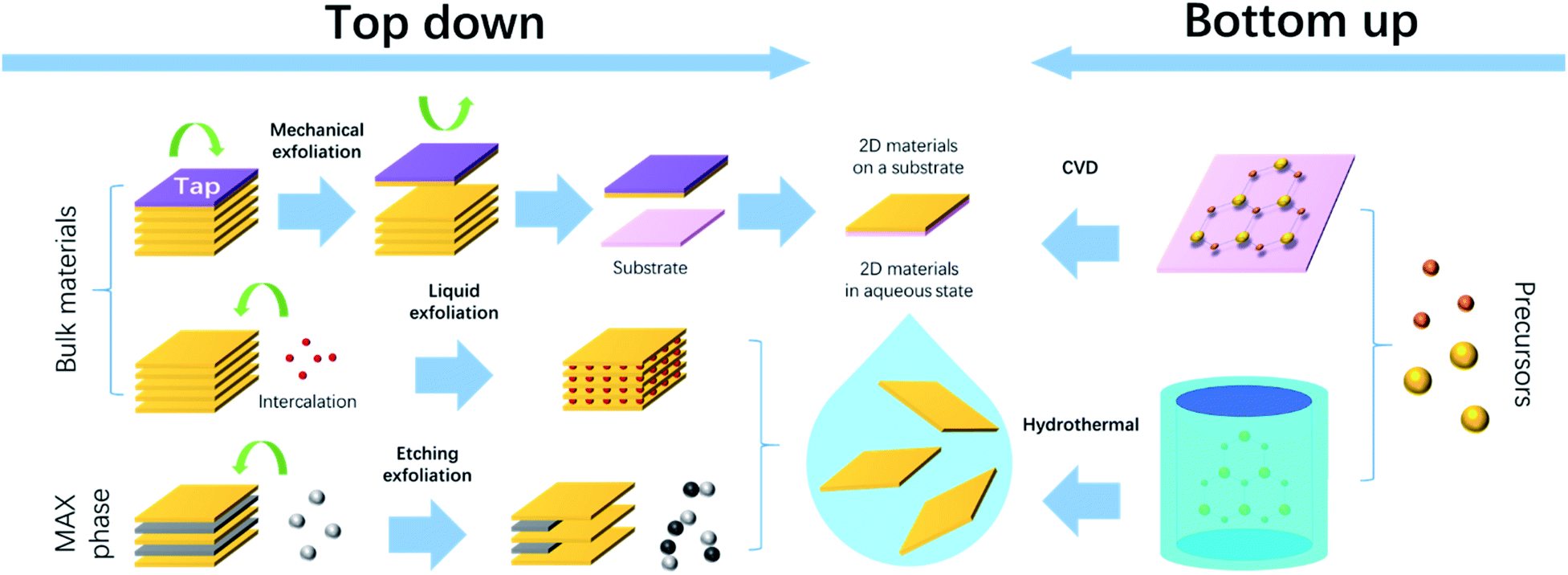 | ||
| Fig. 7 Schematic graph demonstrating the ordinary synthetic approaches to 2D materials. | ||
3.2. Liquid exfoliation
Liquid exfoliation is another widely used top-down method for 2D TMD synthesis.147–150 It can not only reduce the vertical thickness of materials down to the monolayer level, but also shrink the lateral particle size.151 There are several mechanisms, such as one intercalation exfoliation is to insert intercalation ions into TMD interlayers that can expand the layer distance and separate individual layers. Another sonication-assisted exfoliation is to break the vdW bonds between TMD interlayers using ultrasonic energy. A recently reported etching exfoliation is to etch MAX (A = Al, Si, Ge, etc. and X = C, N, P or S) phases using the HyZ gas (Z = S, Se or Te).152 Like the selective etching approach to MXenes,153 the A layer was removed from MAX by the reaction with HyZ, leading to the products of MX2 (TMD) solids and AZ vapor. Despite different mechanisms, all liquid exfoliation processes are undertaken in an aqueous environment, and it is challenging to select an appropriate solvent. Polymer solvents such as cyclohexyl-pyrrolidone (CHP) and N-methylpyrrolidone (NMP) exhibit surface energy matching TMDs, and can avoid aggregation.154–156 Water or inorganic salts with high surface energy lead to a high possibility of reaggregation, but it can be solved by the addition of stabilizers, such as sodium cholate157 and DNA/RNA nucleotides158 that show strong vdW bonding to TMDs. The liquid exfoliation method takes advantage of easy operation and little chance to induce lattice distortion and is universal to most TMDs. In terms of flexible electronic fabrication, the aqueous processing environment is favorable for the chemical decoration of TMDs towards specific applications. NMP acts as a donor dopant to TMDs and enhances electrical mobility, which is beneficial for the integration of transistors.159 Urea solution has been used for the liquid exfoliation of MoS2 and WS2.160 The intermediate NH3 promotes the replacement of nitrogen with sulfur and enhances the catalytic activity of TMDs. In addition, the liquid exfoliated TMDs are in the form of a composite suspension, which can be used as inks for printing or spin coating, to fabricate thin-film electronics.161,1623.3. CVD
The chemical vapor deposition (CVD) technique is a reassuring bottom-up method that takes advantage of delivering precise and controllable fabrication of 2D layered materials by optimizing the reaction parameters, such as temperature, precursors, pressure, duration time, etc. MoS2 can be synthesized by the thermolysis of (NH4)2MoS4.163–166 From 400 °C to 800 °C, MoS2 nanoflakes can be grown from monolayer to few layers (4–6 layers) with the lateral area up to tens of nanometers. Hence, tuning the temperature can effectively lead to different layers of MoS2 stacks. The precursor is another parameter that contributes to controlling the TMD growth. The study of the growth mechanism of MoS2 flakes reveals that vapor MoS2 can directly precipitate on substrates under the sufficient sulfur conditions, while an insufficient sulfur condition results in the presence of solid intermediates.166 Volatile precursors have been used for WS2 nanotube fabrication, leading to complete mixing of the precursors and precise controlling of supersaturation.167 The H2 pulse was employed to alter the reduction environment of WSe2 and enhance the WO3−x flux.168 Monolayer, bilayer, and trilayer WSe2 can be formed when one, two, and three times of H2 pulse were applied, respectively. Therefore, the thickness of TMD films can be controlled and adapted to flexible applications.Most CVD methods require a high processing temperature that is not suitable for polymer substrates, and hence, thermotolerant substrates such as metal foil or silicon oxides are commonly used. Metals are bendable, conductive, and even favorable for the epitaxial growth of TMD single crystals.169 However, the issue of creep and fatigue limits their flexible applications. Silicon oxides are both thermally and chemically stable, but their rigidity is undesirable for flexible electronics. Alternatively, transfer methods can be used to pass the TMD films onto polymer substrates. A transfer media is essential, which can be a poly-methylmethacrylate (PMMA) layer170 or a thermal release tape.171 In another case, TMD thin films are CVD-grown on a substrate that is pretreated by the diluted hydrofluoric acid (DHF). It provides a hydrophilic SiO2/Si surface, and the TMD thin film can be separated from SiO2/Si when immersed into water. This allows the re-deposition of TMD thin films on arbitrary flexible substrates.57 Therefore, the CVD method contributes to the realization of multiple flexible TMD-based electronics, such as transistors,170,171 inverters,57 photodetectors,172 sensors,173etc.
3.4. Hydrothermal reaction
The hydrothermal method, or wet chemistry method, refers to a bottom-up chemical reaction occurring in an aqueous environment with a temperature above 100 °C. Typically a Teflon-lined stainless-steel autoclave is used as the container. The optimization of precursors and reaction conditions (temperature, pH value, atmosphere, etc.) contributes to the modulation of the nanoparticle size and homogeneity. Chen et al.174 demonstrated the conventional low-temperature hydrothermal synthesis of TMD nanocrystals. Using Na2S2O3 and Na2Se2O3 as the chalcogen sources, various TMDs, such as MoS2, MoSe2, NiS2, CoS2, FeS2, etc. were fabricated.The hydrothermal method takes advantage of large-scale manufacture, low processing temperature, easy operation, and the possibility of modifying TMD properties. Doping is a common strategy that can be achieved by hydrothermal methods and used to tailor the TMD band structure. It has been reported that P-doped MoS2 shows an enhanced light absorption range that shows potential for flexible photodetectors,175 while Mn-doped MoS2 exhibits increased active sites, which are favorable for the hydrogen evolution reaction (HER).176 On the other hand, hydrothermal methods have been used to produce TMD composites. The 1T/2H-MoSe2 heterostructure has been hydrothermally synthesized, and consists of both metallic and semiconductive phases.177,178 Due to the enhanced active sites along the phase boundary, the material can be integrated into flexible sensors or hydrogen evolution catalysts. Numerous studies on TMD/CNT composites by hydrothermal methods have been carried out for the flexible energy storage device fabrication.179 The synthetic route allows the TMD nanosheets to grow on CNTs homogeneously, leading to the enhanced specific areas and promoted device charge storage. Therefore, the hydrothermal method is a promising approach to diverse flexible devices.
4. Flexible devices based on TMDs
4.1. Thin film transistors (TFTs)
The synthesis of TMD monolayer films or few-layer suspensions facilitates the realization of flexible electronics. Being the footstone of flexible electronic devices, TMD-based thin-film transistors (TFTs) have attracted intensive interest due to the tunable bandgap, high flexibility, high surface area/volume ratio, and low vertical integration degree of TMDs.180 Different from the bulk field-effect transistors (FETs), TFTs have two dimensions where the surface states have a great impact on their switching characteristics. For example, monolayer MoS2 shows a higher density of S vacancies than their bulk states, leading to an increased state density.180 These atomic defects are potential charge traps and responsible for charge leakage. Besides, the intrinsic electron–phonon scattering, Coulomb impurities, surface roughness, charge traps, etc. also threaten the electronic performance of the TFTs.181 To address these issues, strategies have been explored such as doping and heterostructuring, employing high-k dielectrics to minimize the charge scattering, promoting a smooth contact surface to reduce the Schottky barrier, and developing advanced device architecture to boost charge transportation, etc.Dielectrics. The proper dielectric material is expected to show high relative permittivity which can screen Coulomb impurities and improve the field-effect mobility.182 Dielectrics of Al2O3 and HfO2 with a high-k value have been investigated in various TMD systems.183–185 It has been reported that a HfO2 dielectric layer results in a field-effect mobility of 40 cm2 V−1 s−1 for MoS2 back-gated FETs. The near-ideal SS and on/off current ratio can reach 77.6 mV dec−1 and 106.186 As for TFTs, the high-k dielectric layer should also exhibit high flexibility, and this requires the dielectric thickness to be minimized. Nevertheless, the TMD surface remains a challenge of depositing the uniform dielectric layer because of the dangling bond shortage.187 Therefore, doping and heterostructure strategies have been used to achieve an proper TMD surface state.159,188 The graphene single layer is pre-deposited on MoS2 to assist the subsequent deposition of the ultrathin HfO2 gate dielectric.189 The presence of graphene not only promotes the growth of the HfO2 layer by providing a proper interface roughness but also shrinks the gate leakage. Besides, the n-type doping nature of the graphene monolayer can effectively reduce the contact resistance resulting in outstanding switching characteristics. The effect of Al-doped HfO2 dielectrics on MoS2-based FETs has been studied, and the results are presented in Fig. 8a.190 The presence of Al in HfO2 contributes to passivating the defects at oxygen vacancies and filling the porous structure of HfO2, leading to high densification and a smooth HfO2 surface. The similar effects of Al as a dopant have been reported in ZrO2 dielectric as well.191 This facilitates the deposition of Al-doped HfO2 or ZrO2 ultrathin films on TMDs.
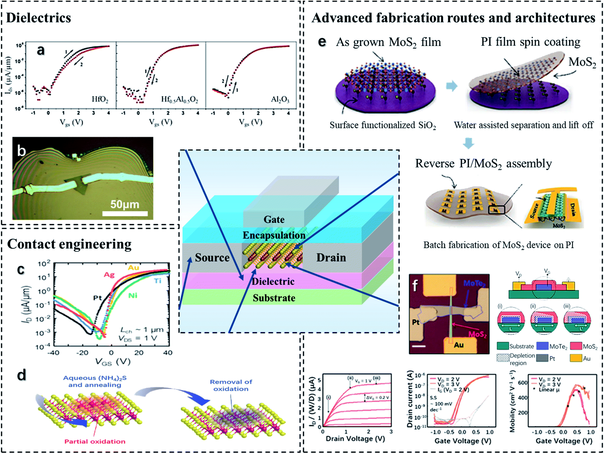 | ||
| Fig. 8 Strategies towards boosting the TMD-based TFT performance. (a) Effects of Al-doping and high-k dielectrics on the enhancement of MoS2 transistors. Reproduced with permission from ref. 190, copyright 2019 The Japan Society of Applied Physics. (b) Ion gels are used as flexible dielectrics for MoS2 TFTs. Reproduced with permission from ref. 211, copyright 2017 Scientific Reports. (c) Effects of different contact materials on the electrical performance of MoTe2 transistors. Reproduced with permission from ref. 193, copyright 2019 Nano Letters. (d) Contact engineering by thermal treatment to remove defects. Reproduced with permission from ref. 197, copyright 2020 Advanced Functional Materials. (e) Advanced damage-free method to transfer MoS2 thin films on flexible substrates. Reproduced with permission from ref. 57, copyright 2018 Advanced Functional Materials. (f) The scheme and switching characteristics of the n-channel JFET with a heterojunction of MoS2/MoTe2. Reproduced with permission from ref. 206, copyright 2018 npj 2D Materials and Applications. | ||
Contact engineering. The enhancement of the contacts of TFTs involves the contact material selection and surface treatments. A desirable contact material should lead to a low Schottky barrier and contact resistance. For TMDs with a large bandgap, contact metals with lower work functions are preferred for suppressing the Schottky barrier leading to better electrical properties (Fig. 8c).192 Some commonly used metal contacts with their work functions include Au (5.1 eV),193 Al (4.54 eV),192 Ti (4.33 eV), Ag (4.26 eV),193 Sc (3.5 eV),194etc. With a relatively lower work function, Al introduces less ohmic contact than Au towards MoS2, leading to a smaller Schottky barrier height (SBH) of 7 meV.195 Ag-contacted MoTe2 presents an impressive saturation current of 400 μA μm−1 and low contact resistivity of 1.2 kΩ μm at 80 K.193 Owing to the extremely low working function, Sc is regarded as a propitious contact material. However, Sc may interact with chalcogens due to the high reactivity of Sc. This leads to the reduction of the transition metals from TMDs, which commonly have higher working functions than Sc and increase the SBH. To address the issue, several approaches have been proposed. Mleczko et al.193 introduced a BN contact interlayer, which not only prevents the interactions between Sc and Te but also softens the Fermi level pinning effect in MoTe2. It results in a significantly reduced SBH of 80–100 meV, which is much lower than that of Ag-contacted MoTe2. Alternatively, Smyth et al.194 used an ultra-high vacuum (UHV) synthetic method to deposit Sc contacts on the WSe2 FETs. With the exclusion of post-metallization, a passivated oxidation layer is formed at the contact surface which prevents the reaction between WSe2 and Sc, leading to the decrease of the SBH. The as-fabricated transistor shows a minimum SBH and subthreshold swing (SS) reaching 0.1 eV and 109 mV dec−1, resulting in an on/off current ratio of 106.
In addition to contact material selection, a proper surface treatment can effectively produce a high-quality contact surface and improve transfer performance. It has been indicated that the Fermi level is pinned below the conduction band of TMDs that is responsible for the SBH at the contact metal/TMD surfaces.196 To address the issue, one effective method is using the thermal treatment to enhance the crystallization of TMDs and remove the residual reactors. Besides, the treatment is damage-free that leads to an interface with few defect states (Fig. 8d).197 Alternatively, an H2S-assisted CVD method can be used at a low synthetic temperature to deposit an additional layer of S on the TMD surface. The substitution of S fills in the vacancies at the TMD surface and introduced acceptor states. This contributes to the hole injection as the Fermi level is pinned at the maximum of the valence band (VBM).198 With exposure to oxygen plasma, a TiOx/MoS2 contact interface can be formed in a Ti-contacted MoS2 transistor.199 The TiOx layer contributes to depinning of the Fermi level near the MoS2 conduction band and reducing the SBH by removing the surface positive charges.
Device architectures. Another strategy to boost the TFT properties is to modify the device architecture. Encapsulation is an effective way to protect the device from air oxidation, suppress the SBH, and reduce the Coulomb scattering, leading to an increased field-effect mobility.193,200–202 The top-gate dielectric encapsulation of HfO2 can improve the electron mobility of a single-layer MoS2-based TFT from 0.1–10 to ∼200 cm2 V−1 s−1.44 For another case, the mobility of a MoS2-based transistor has been increased by 40% with a significant reduction of hysteresis by Al2O3 encapsulation.201 To enhance flexibility, polymer encapsulation has been used in MoS2-based FETs.203,204 The additional polymer layer induces mechanical strain at the interface that contributes to reducing the surface adsorbates and gaining contact areas. In addition to the encapsulation, researchers have developed several novel device geometries to inhibit the defects. The SiO2/MoS2 core–shell heterostructure gates and channels have been integrated into an Ω-shape.205 The geometry takes advantage of avoiding the wet transfer process and minimizing surface contamination. The on/off ratio of the as-fabricated device shows a comparable value of 0.02 cm2 V−1 s−1. A 2D TMD heterojunction-based junction field-effect transistor (JFET) has been constructed, which consists of connected n-type (MoS2) and p-type (MoTe2) diodes with a vdW interface.206 As illustrated in Fig. 8e, the n-type channel is gated by the p-type material and vice versa. Owing to this unique design, the device can conduct both electron and hole carriers simultaneously. Besides, due to the low defect density at the vdW p–n junction interface, it exhibits neglected hysteresis and an improved in-plane current. A crested substrate has been proposed to enhance the roughness-dependent mobility.207 It is reported that the surface roughness of the TMD/substrate can induce a strain field that shows positive effects on reducing the bandgap and effective carrier mass. Hence, compared to the normal substrate, the device with crested substrates exhibits electron mobility increasing from 6.5 to 285 cm2 V−1 s−1 for the n-type MoSe2-based FET, and a tenfold increase in hole mobility for the p-type WSe2-based FET.
Device flexibility. Several approaches towards device performance enhancement have been discussed in the sections above. However, it is a crucial task to boost the performance without sacrificing the flexibility. Hence, ductile materials and advanced device fabrication routes are strongly recommended. Flexible dielectrics have been employed to adjust the gate screening effects and enhance the flexibility of TMD-based TFTs. The copolymer dielectric, poly(2,4,6,8-tetramethyl-2,4,6,8-tetravinylcyclotetrasiloxane-co-cyclohexyl methacrylate) [p(V4D4-co-CHMA)], has been deposited via the CVD method on a MoS2-based TFT.208 Owing to the conjugated network structure and the cyclohexyl groups, [p(V4D4-co-CHMA)] enhances the electrical strength and effectively suppresses the charge traps at the MoS2 interface. Ion gels are another class of flexible dielectrics for TMD-based TFTs (Fig. 8b).209,210 These materials are highly stretchable and exhibit high ionic conductivity. Besides, they show a large specific capacity that can screen the surface phonon scattering and boost the device mobility. However, ion gels may exhibit high leakage current leading to the decrease of the on/off current ratio. Hence, additional leakage current barriers, for example, an Al2O3 thin film, can be intercalated between the ion gel and TMD surfaces to prevent the capacitance drop.211
Alternatively, for TMD-based TFT fabrication, conventional methods such as CVD and atomic-layer deposition (ALD) can lead to a precise deposition and minimize the defect state.212,213 However, the subsequent transfer of TMD films to flexible substrates may result in the production of unavoidable defects and damages, which harm the device's electronic behaviors. One solution is to use damage-free transfer methods, which have been introduced in the previous section. Another one is to directly deposit TMDs on flexible substrates. Metal-assisted synthesis can reduce the sulfurization temperature of TMDs, which brings the possibility of growing TMD films directly on polymer platforms via CVD methods. As reported, Au particles can provide nucleation sites for TMDs at low temperatures, leading to an improved crystallinity and enhanced device performance.214 Similarly, the presence of Ni can also reduce the synthetic temperature to 400 °C for WS2 and 500 °C for MoS2.215
To summarize, principles for the improvement of the TMD-based FET performance include materials, interface engineering, device design, etc. Material engineering contributes to the enhancement of the intrinsic manner of each component, while contact engineering aims at the control of charge flows through the component interfaces. Both approaches can effectively reduce the SBH, defect density, and carrier scattering, leading to high carrier mobility and good gate control. Beyond these methods, the device design is a novel strategy to adapt the device to additional uses. As aforementioned, the Ω-shaped gate is suitable for the integration of 3D FETs, and the JFET is capable of conducting both electron and hole carriers. The crested substrate design can be potentially combined with the wavy configuration for the future flexible and stretchable applications.
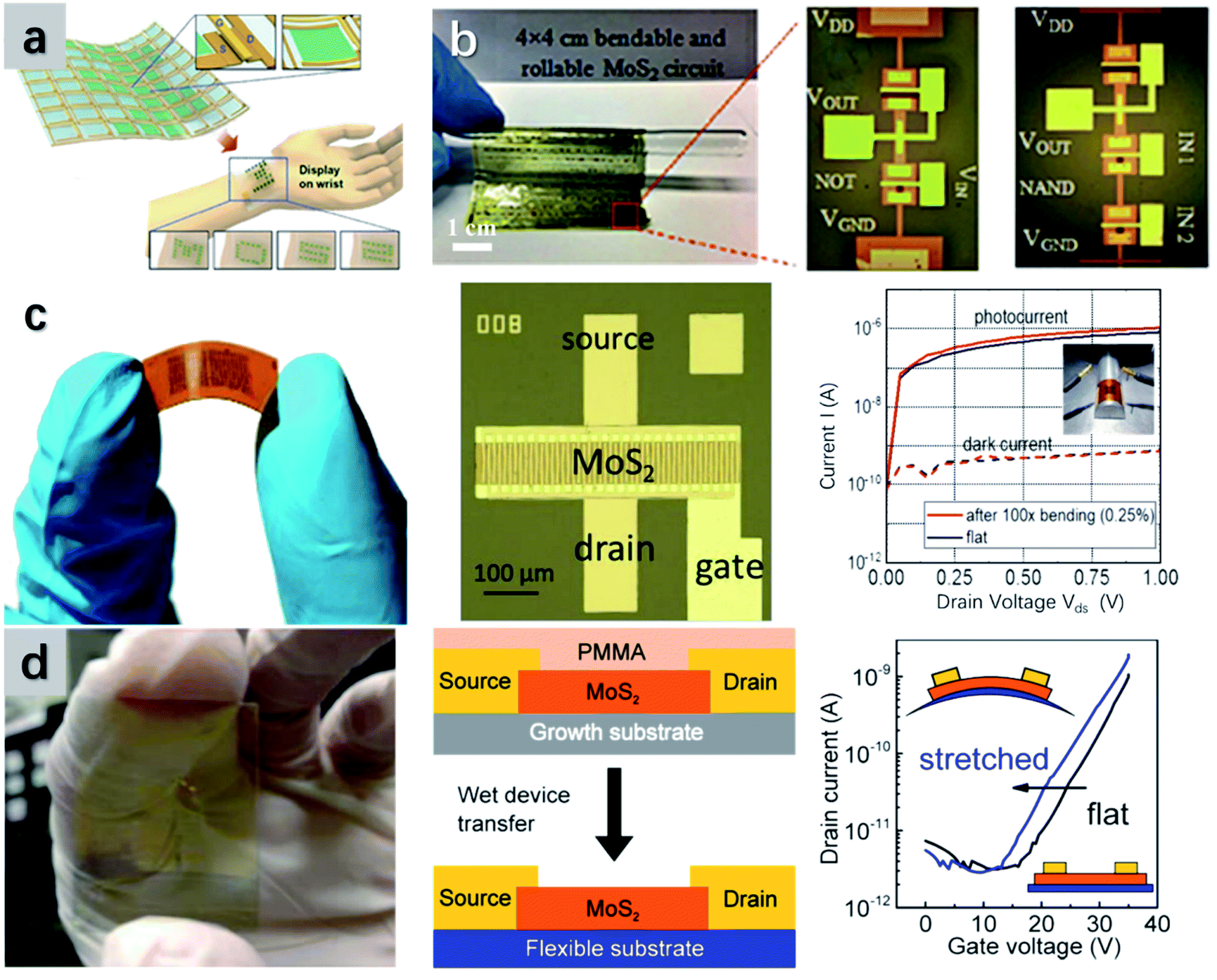 | ||
| Fig. 9 Different flexible applications of TMD-based TFTs. (a) Schematic illustration of the wearable OLET display controlled by a MoS2 TFT. Reproduced with permission from ref. 59, copyright 2018 Science Advances. (b) The fabrication of an inverter based on MoS2 TFTs on a flexible paper. Reproduced with permission from ref. 57, copyright 2018 Advanced Functional Materials. (c) Image of a flexible photodetector built from MoS2 TFTs. The device shows excellent detectivity towards light after 100 bending cycles. Reproduced with permission from ref. 221, copyright 2020 ACS Photonics. (d) Photograph of a transparent and flexible strain sensor built on MoS2 TFTs. The device is fabricated via a wet transfer method and shows outstanding sensitivity towards stretching. Reproduced with permission from ref. 225, copyright 2015 ACS Applied Materials & Interfaces. | ||
Beyond these conventional applications, TMD-based TFTs are more favorable for photodetectors. This is due to the tunable bandgaps of TMDs towards the photoexcitation. Besides, the moderate bandgap (around 2 eV) and the thickness-dependent indirect/direct bandgap transition of few-layer TMDs are feasible for ultraviolet to near-infrared applications.218,219 By controlling the TMD layer number or using complex heterostructures, the bandgap can be desired for the specific detection of light with a certain wavelength range. Qin et al.220 employed a laser writing method to precisely synthesize MoS2 monolayers. The photoluminescence spectra of the MoS2 single layer can be controlled within the range between 1.77 eV and 1.82 eV. However Schneider et al.221 proposed a soft photodetector (Fig. 9c) based on few-layer MoS2 (3–4 layers), which exhibits photoluminescence spectra around 1.83 eV to 1.96 eV. The specific detectivity can be further enhanced by electrostatic gating, reaching 1012 to 1010 Jones. The device also presents a maximum responsivity of 540 A W−1 at Vgs = 0 V, which can be further improved by additional MoS2 layers. In another case, a thin-film photodetector based on MoS2 nanoflowers was fabricated.222 The high specific area of MoS2 nanoflowers enhances the effective area of the channel and improves the device sensitivity. The device can show fast responses in the entire visible light range and barely present degradation under bending at 0.75 cm. To improve device flexibility, printing and screening methods have been widely used.223 For example, a printed photosensor with WS2 tunneling layers shows a high sensitivity of 0.61 mA W−1 and high flexibility when integrated onto a paper substrate.224
The strain sensor is another application where TMD-based TFTs have been utilized. This should be attributed to the strain-dependency bandgap of TMDs. For example, in terms of monolayer, bilayer, and trilayer MoS2, the bandgap decreases with the strain at rates of −0.05, −0.12, and −0.3 %strain−1, respectively.225 Besides, MoS2 exhibits a Fermi level shift towards the conduction band edge upon the strain at a rate of −0.19 to −0.24 %strain−1. Hence, as shown in Fig. 9d, a TFT has been fabricated with MoS2 as the channel and an Al2/ITO/PET plastic layer as the substrate. The device presents a large on/off current ratio of 104 and reliable stability over 180 cycles at the bending radius up to 0.9 cm. Given a Vbg of 20 V, the thin-film MoS2-based sensor delivered a sensitivity of −40, which is 1.3 times higher in comparison with that of conventional silicon-based sensors. In another case, an unstrained MoS2/PI TFT exhibits an on/off current ratio of 5600 and high mobility of 7.07 cm V−1 s−1. When bent at 1 cm, the transistor maintains 55% of the on/off ratio and 75% of the mobility.226 With superior mechanical stability, the TFT has been integrated into a strain sensor. When optimized stress is applied, the indirect/direct bandgap transition of MoS2 can be initiated, resulting in the change of the photocurrent. Naqi et al.227 proposed a MoS2 TFT for ultrasonic detection. The TFT shows a high on/off ratio of 105 and outstanding switching characteristics over 10 to 500 kHz. Besides, the detector exhibits consistent performance over 2000 bending cycles at 5 mm. Compared to MoS2, MoSe2 is more feasible for TFT applications due to its relatively narrower bandgap with a better tunneling probability and a lower subthreshold swing.228 Thus, a flexible MoSe2-based strain sensor has been fabricated. Under the strain, the device exhibits little changes in the on/off current ratio and the SS value, delivering a sensitivity of 3.61 towards a strain of 2%.
4.2. Energy storage
000 cycles. In another case, a free-standing MoS2/RGO electrode has been vacuum-filtered on a cellulose membrane.234 The as-obtained thin film electrode exhibits excellent flexibility as demonstrated in Fig. 10a. On the basis of the good stability of MoS2/RGO, the electrode accommodates 5000 cycles at 4 A g−1. Besides, RGO lowers the device internal resistance, resulting in a low iR drop of 0.026 V at 1 A g−1. Finally, the capacitance of the electrode reaches 365 to 227 F g−1 at 0.5 to 10 A g−1.
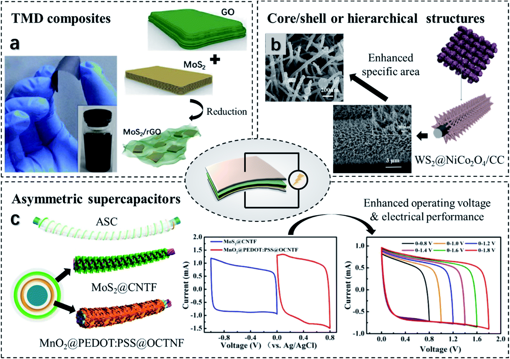 | ||
| Fig. 10 Strategies towards high-performance flexible TMD-based SCs. (a) The fabrication of a free-standing MoS2/RGO film as the SC electrode. Reproduced with permission from ref. 234, copyright 2019 Solid State Communications. (b) A WS2@NiCo2O4/CC electrode with a core/shell structure leading to an enhancement of the specific area. Reproduced with permission from ref. 238, copyright 2020 ACS Omega. (c) A fibrous core/shell ASC with MoS2@CNTF and MnO2@PEDOT:PSS@OCTNF electrodes. The two electrodes exhibit positive and negative CV behaviors, respectively, leading to an increased voltage window when integrating into an ASC. Reproduced with permission from ref. 233, copyright 2017 Nano Energy. | ||
To further enhance the device storage performance, TMDs can be composited with conductive polymers, such as polypyrrole (PPy) and polyaniline (PANI).235,236 The porous structure of conductive polymers not only offers stretchable support but also provides a high specific area resulting in high capacitance. Alternatively, core/shell structures have been widely used for flexible SCs with large capacitance. For example, a wire-shaped electrode with a CF core and a TiO2@MoS2 shell has been developed.237 The electrode possesses a high linear capacitance of 1740 μF cm−1 at 0.02 mA as a result of enormous active sites of MoS2 nanoparticles. Besides, the fibrous configuration is favorable for wearable device fabrication. As illustrated in Fig. 10b, a solid-state WS2@NiCo2O4/CC flexible SC with a hierarchical structure was manufactured.238 Taking advantage of the layered structures of WS2, the electrode shows a shortened ion diffusion path and an enhanced conductivity. Hence, it exhibits an areal capacitance reaching 1878.4 mF cm−2 at 2 mA cm−2. In terms of flexibility, the device can bear bending within an angle ranging from 0° to 180° and shows no apparent capacitance loss under stain when working at 10 mV s−1. Another strategy to open the cell voltage is fabricating asymmetry supercapacitors (ASCs) that contain two different electrodes. Zhang's group233 developed a fiber-shaped ASC with a positive electrode of MnO2@PEDOT:PSS@oxidized carbon nanotube fiber (OCNTF) and a negative electrode of MoS2@CNTF (Fig. 10b). The two electrodes exhibit high capacitances of 837.6 and 723 mF cm−2, respectively. As a combination, the asymmetry SC exhibits an improved capacitance of 278.6 mF cm−2 when the current density is 0.6 mA cm−2, with the corresponding power density reaching 540 μW cm−2. Moreover, such an SC yields a stretchable strain of 100% and maintains 92% of the specific capacitance over 3000 stretching runs. An ASC sheet has been built upon a pair of MoS2/PEDOT/CNT (positive) and SnS2/CNT (negative) electrodes. At 1.5 mA cm−2, it discloses a potential window of 1.7 V and a specific capacitance of 103.76 mF cm−2. Besides, it presents excellent waterproofness and stretchability up to 225% without capacity degradation.239 Kumar et al.240 constructed ASC containing RGO and WO3/WS2 core/shell electrodes. The individual electrodes exhibit an areal capacitance above 55 mF cm−2 and capacity retention of >90% over 10000 cycles. As a result, the ASC shows a large voltage window of 1.5 V and 70% capacity retention after 10000 cycles. It also maintains 97% of the capacitance at 90° bending, implying its superior flexibility. A hierarchical electrode with MnS2@Ni-mesh and MoS2@Ni-mesh electrodes has been reported.241 The role of Ni-mesh is to enhance flexibility, facilitate ion diffusion, and improve electrochemical stability. The electrode exhibits an area capacitance of 7.4 mF cm2 at 10 mV s−1, and retains 80% of the capacitance over 5000 cycles. A large voltage window of 1.6 V and a power density of 16 W cm−2 are also obtained. The ASC withstands a bending radius up to 2 mm with a maximum capacity drop of 9%, and bear 1000 bending cycles at 5 mm with almost unchanged electrical properties.
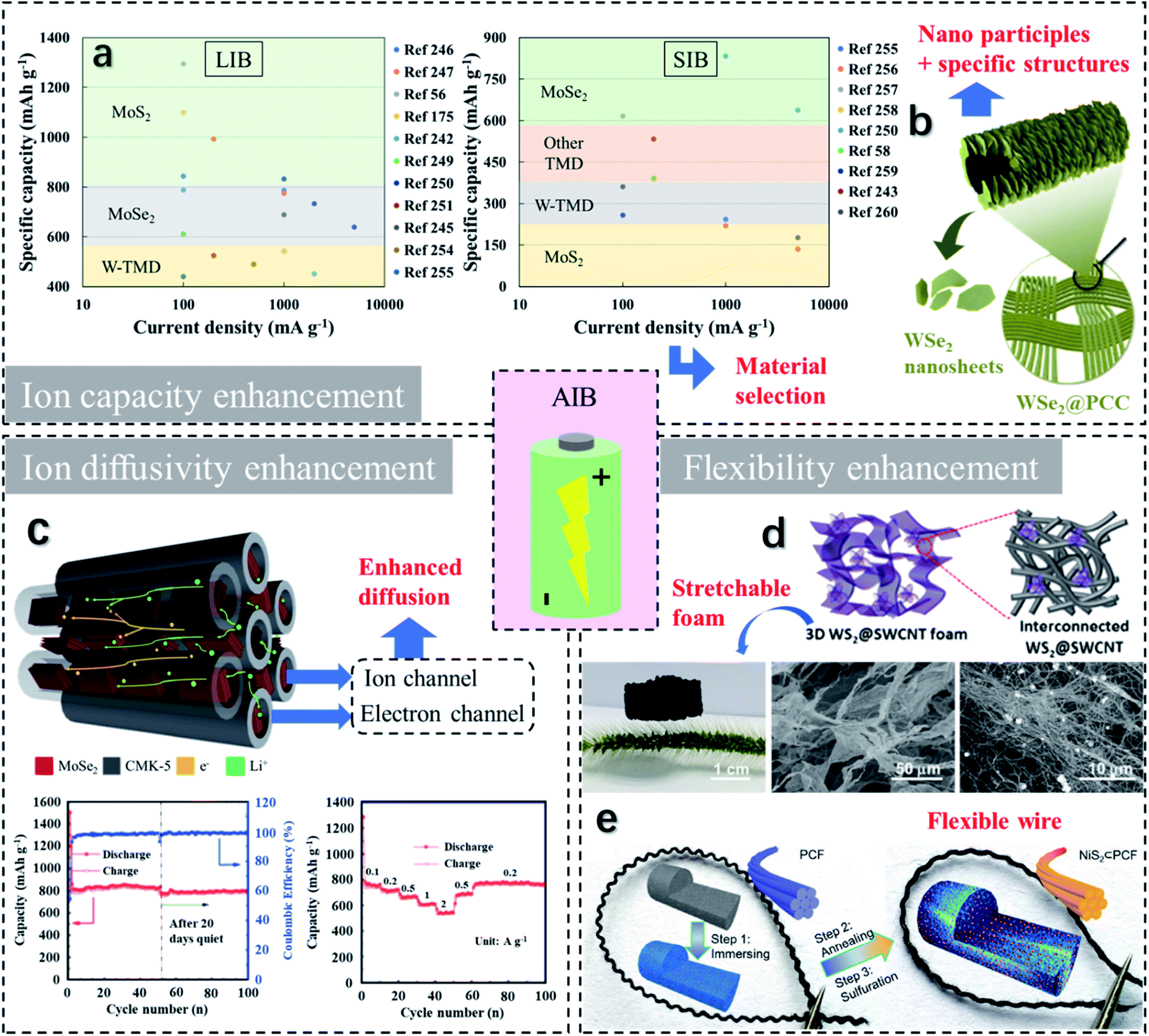 | ||
| Fig. 11 Approaches towards improvement of the properties of flexible alkali-ion batteries, including the ion capacity enhancement, the ion diffusivity enhancement, and the flexibility enhancement. (a) Summary of some recent studies on TMD-based AIBs, indicating the effects of TMDs on ion capacity improvement. (b) Increased specific area (via nanoparticles, porous foams, core/shell structures, hollow structures, etc.) contributes to promoting the ion capacity. Reproduced with permission from ref. 249, copyright 2020 Journal of Alloys and Compounds. (c) Carbon hybrids/heterostructures are the most common strategy for boosting AIB charge/ion diffusivity. Reproduced with permission from ref. 247, copyright 2017 Journal of Materials Chemistry A. (d and e) Flexibility enhancement can be achieved by employing carbon cloths, stretchable 3D foams, fibrous structures, etc. Reproduced with permission from ref. 250, copyright 2018 Electrochimica Acta and ref. 248, copyright 2018 Advanced Energy Materials. | ||
Numerous studies on MoS2-based LIBs have been recently reported, revealing that most of MoS2-based LIBs are composed of carbon composites. In Fig. 12a, Wang et al.251 presented an anode design of few-layer MoS2 particles vertically grown and anchored on flexible RGO substrates. At 100 mA g−1, the MoS2/RGO anode displays a specific capacity of 930 mA h g−1 and capacity retention of 84.7%. At 1000 mA g−1, the electrode survives over 1000 cycles with a discharge capacity of 786 mA h g−1 in line with a capacity retention of 96.4%. In another case, as shown in Fig. 12b, a hollow structured C@TiO2@MoS2 anode with a carbon interlayer, a TiO2 middle layer, and a MoS2 outer layer has been developed.252 Beyond the beneficial effects of the carbon inner shell, the flexible TiO2 shell also shortens the Li+ diffusion distance and boosts the rate capacity. Besides, the hollow architecture provides a void core with high-volume expansion and abundant active sites. Hence, at 200 mA g−1, the electrode presents an initial and specific capacity of 1687 and 993.2 mA h g−1, respectively. Besides, a long-term reversibility performance of 600 running cycles is presented in Fig. 12c. It reveals that the anode delivers a reliable remaining capacity of 775.2 mA h g−1. To enhance the device flexibility, ultra-thin-film anodes were developed. Lin et al.60 demonstrated an extremely flexible anode fabricated with 1T/2H MoS2 nanosheets grown onto the carbon fiber cloth (CFC) with SnS2 nanoparticle decoration (Fig. 12d). The SnS2/MoS2/CFC anode has several advantages, such as (1) the connected carbon fibers build a fast diffusion network for electrons and Li ions; (2) the electrode is highly flexible and accommodates to rolling up to 360°, see Fig. 12e; (3) the vertical alignment of MoS2 nanoparticles on the CFC leads to high specific surface areas and a short diffusion distance for electrons and Li ions and (4) during charging/discharging, SnS2 nanoparticles protect the electrode from pulverization. The electrochemical performance of SnS2/MoS2/CFC is illustrated in Fig. 12f. At 100 mA h g−1, a capacity of 1294 mA h g−1 is retained after 120 cycles. Comparatively, the MoS2/CFC electrode without SnS2 coating survives after 60 cycles but presents a severe capacity reduction from 1100 to 580 mA h g−1 after 120 cycles. When matched with a conventional LiCoO2 cathode, the full cell delivers an initial discharge capacity of 177.6 mA h g−1, 51% of which is maintained after 50 cycles. In a different case, amorphous MoS2 (A-MoS2) nanoflakes are deposited on the N-doped carbon microtubes (NCMTs). The composites were cross-linked to an RGO film and formed an NCTMs@A-MoS2/RGO flexible paper.179 Compared to crystalline MoS2, A-MoS2 takes advantage of easy fabrication, which requires low temperature and a short time. In addition, A-MoS2 provides percolation pathways for fast transportation of Li ions through the opening of active diffusion channels. Besides, it bears the high strain and volume deformation by virtue of the low grain boundary density. Therefore, at 500 mA g−1, the initial discharge specific capacity of the electrode is 1045.5 mA h g−1. With a doubled current density, it maintains a capacity of 544 mA h g−1 after 1000 cycles.
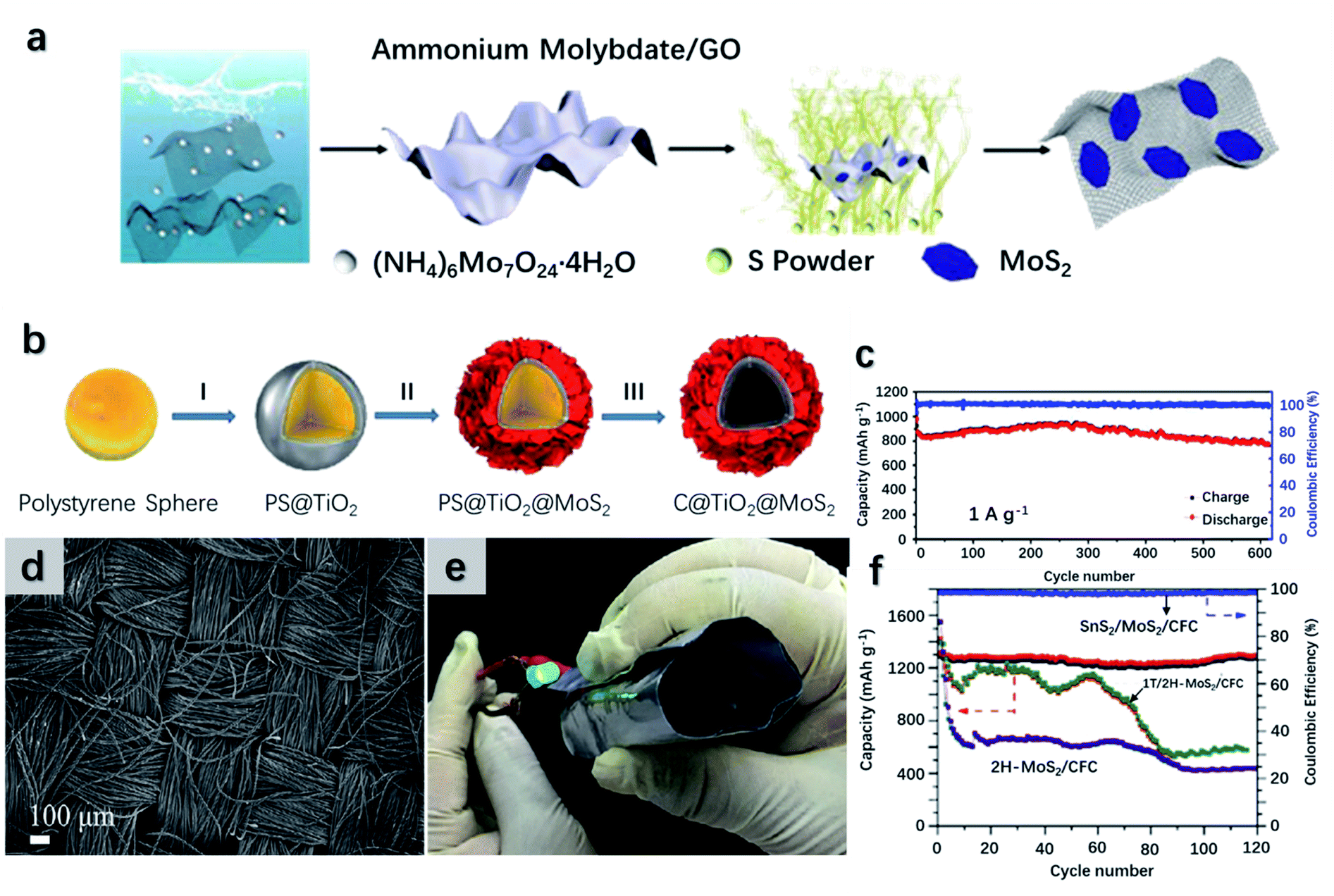 | ||
| Fig. 12 (a and b) Graphic scheme of the synthetic process of MoS2/RGO and C@TiO2@MoS2 composites, respectively. Reproduced with permission from ref. 251, copyright 2019 Particle & Particle Systems Characterization and ref. 252, copyright 2018 Nanoscale. (c) Cycling performance and coulombic efficiency of C@TiO2@MoS2 as an anode at 1000 mA g−1. (d) SEM image illustrating the morphology of SnS2/MoS2/CFC. (e) Photo of the full cell with SnS2/MoS2/CFC as the anode showing its good flexibility. (f) Cycling performance of SnS2/MoS2/CFC, 1T/2H-MoS2/CFC and 2H-MoS2/CFC electrodes at the current density of 100 mA g−1. Reproduced with permission from ref. 60, copyright 2019 Chemical Engineering Journal. | ||
Intensive investigation of MoSe2 and WS2 based LIB anodes as high conductivity and low ion migration barriers have been carried out.253 A MoSe2-based electrode with high rate performance was formed with the encapsulation of ordered mesoporous carbon CMK-5.247 The scheme of the MoSe2/CMK-5 electrode and its electrochemical characteristics are illustrated in Fig. 11c. The mesoporous geometry of CMK-5 provides high surface areas and shortens the Li-ion diffusion pathway, leading to a promoted initial capacity of 1504 mA h g−1 at 100 mA g−1. Similarly, a flexible MoSe2/N-doped polyacrylonitrile carbon nanofiber (HPCF) anode was manufactured.254 An initial discharge capacity of 862.7 mA h g−1 is delivered at 100 mA g−1 with a high initial coulombic efficiency (ICE) reaching 76.3%. A desired rate performance is presented with the specific capacities being 676.2, 451.5, and 398.0 mA h g−1 at 0.1, 1.0, and 2.0 A g−1, respectively. A flexible MoSe2 @ carbon cloth (CC) electrode exhibits reversible specific capacities of 1337, 831, and 749 mA h g−1 at 0.1, 1, and 2 A g−1, respectively.255 The electrode can even withstand extremely high current density up to 5 A g−1 and maintain a capacity of 638 mA h g−1 over 1200 runs. A GF@CNTs@WS2 electrode is designed and can be folded at 180° due to the flexibility of graphene.256 Besides, the electrode exhibits a promising rate performance with discharge specific capacities of 931, 568, and 300 mA h g−1 at 0.1, 1, and 5 A g−1, respectively. As illustrated in Fig. 11d, a 3D hybrid foam has been developed established on WS2-decorated single-wall carbon nanotubes (SWCNTs).250 The WS2@SWCNT electrode shows features of lightweight, high flexibility, and remarkable conductivity. At 100 mA g−1, an initial discharge and charge capacities of 1893 and 1210 mA h g−1 are delivered. After 1000 runs, a capacity of 688.9 mA h g−1 with a capacity retention of 113% can be maintained at 1 A g−1.
Due to the limited lithium storage on earth, SIBs are believed to replace LIBs to fulfill the energy requirements in the future. Though having the same working mechanism, one crucial dissimilarity between SIBs and LIBs is the larger ionic radii of Na+ than Li+. Hence, materials with large interlayer spacing, such as TMDs, are favorable for the insertion and extraction of Na+ leading to promising redox reversibility.257,312 A SIB anode composed of MoS2 particles dispersed onto 3D nanofibers (CNFs) was fabricated via the electrospinning technique.258 The technique involved a polyacrylonitrile-based solution, which can release nitrogen during the process, leading to enhanced active sites and Na+ diffusion rates. Besides, the CNF network provided a flexible and freestanding configuration and a pathway for charge diffusion. Compared to the pure MoS2 electrode, the heterostructure electrode presents improved stability without MoS2 particle agglomeration and reinforces the electrical conductivity. As illustrated in Fig. 13a, the device delivers a specific capacity of 205 mA h g−1 at 2 A g−1, and exhibits a high reversible capacity of 525 mA h g−1 over 70 cycles. Deng et al.259 proposed a hybrid anode composed of Nb2O5, MoS2, hard carbon, and CNFs. The electrode is grounded upon an adsorption–intercalation–conversion mechanism. Nb2O5 and MoS2 are utilized to accelerate the sodium diffusion rate and enhance the sodium capacity, while hard carbon and CNFs are employed to improve the conductivity and flexibility. As a result, the Nb2O5@MoS2@C CNF anode delivers an outstanding capacity of 220 mA h g−1 at 1 A g−1, and capacity retention ratio of 82% at 5 A g−1 stability over 20000 cycles (Fig. 13b). Porous carbon nanofiber (PCNF)@MoS2@TiO2 and PCNF@MoS2@carbon anodes exhibits relatively poor capacities of 216 and 162 mA h g−1 and the retention ratio of 37% and 28%, respectively.260 To improve the device performance, an additional PEDOT layer has been employed, as its high conductivity reduces the impedance and boosts the rate performance. Besides, the PEDOT layer acts as an encapsulation that prevents MoS2 from being pulverized into nanocrystals.260 Accordingly, the PCNF@MoS2@PEDOT anode exhibits upgraded electrochemical properties of the specific capacity reaching 313 mA h g−1 at 20 A g−1 (Fig. 13c). Besides, an excellent flexibility is revealed, as it withstands rolling deformation over 160 times with little changes in the capacity. A flexible MoSe2@carbon fiber (CF) SIB anode has been integrated, as demonstrated in Fig. 13d.261 Compared to the pure MoSe2 electrode, MoSe2@CF benefits from the improved conductivity and sufficient active sites from CFs. Therefore, the initial and retention capacities have been strengthened from 1088.9 to 887.9 mA h g−1 and 282.8 to 390.7 mA h g−1 after 100 cycles. In another study, a highly flexible binder-free MoSe2@CC anode with a hierarchical configuration has been fabricated.255 At 0.1 A g−1, the anode exhibits an initial discharge/charge capacity of 839/650 mA h g−1 with the coulombic efficiency reaching 77.4%. A capacity of 266 mA h g−1 is achieved at 2 A g−1 over 60 cycles, and a reversible capacity of 468 mA h g−1 is maintained when the current density returns to 0.1 A g −1. Furthermore, the MoSe2@CC anode follows a combined surface- and diffusion-controlled sodium-ion diffusion mechanism. With an increasing scan rate, the dominated mechanism switches over from the diffusion-controlled process to the surface-controlled process.
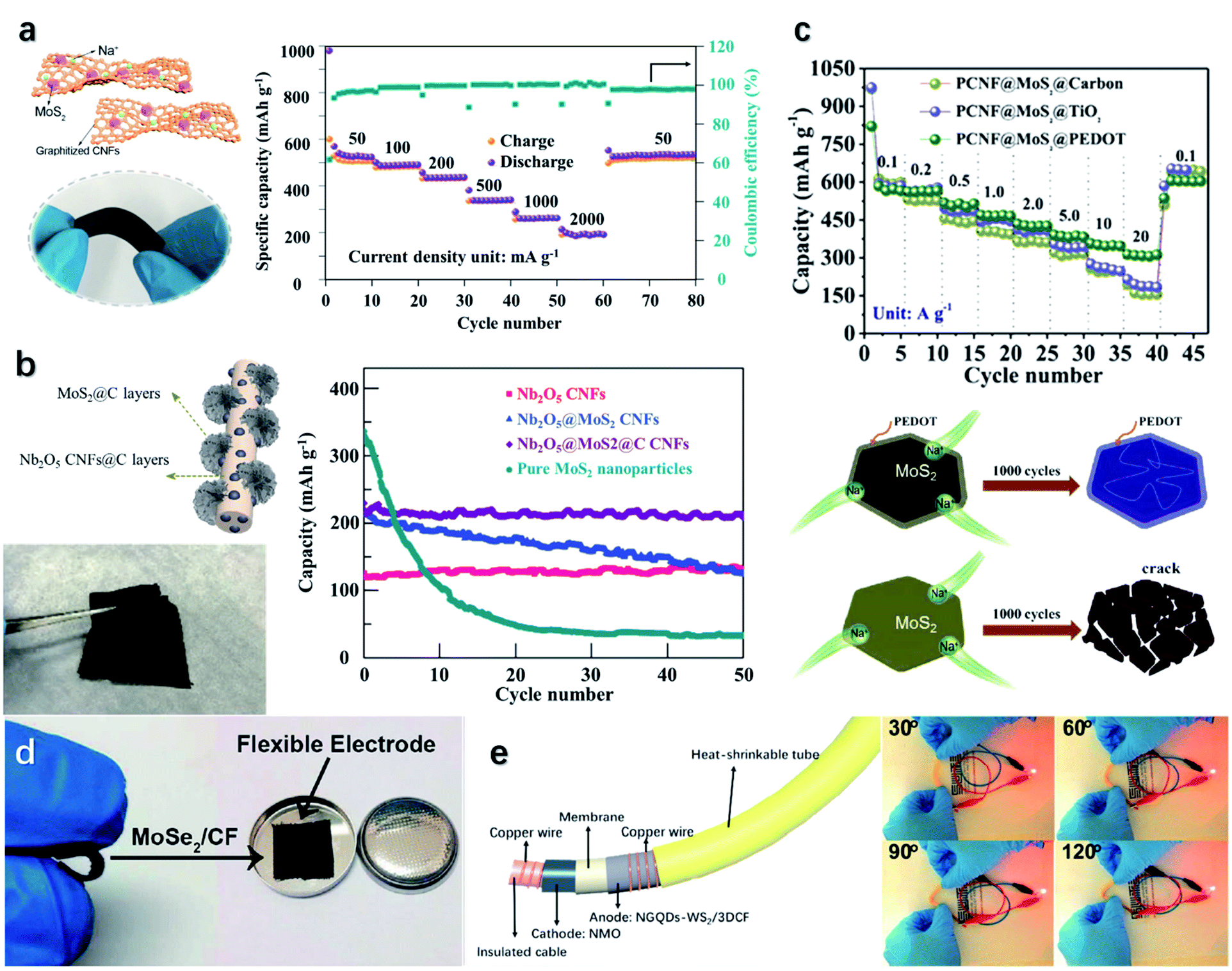 | ||
| Fig. 13 (a and b) The structural and electrochemical features of the MoS2@CNF and the Nb2O5@MoS2@C CNF hybrids as the anodes for SIBs, respectively. Reproduced with permission from ref. 258, copyright 2019 ACS Applied Materials & Interfaces and ref. 259, copyright 2020 Advanced Functional Materials. (c) Cycling performance of the different MoS2-based hybrid anodes and the encapsulation mechanism of the PEDOT layer. Reproduced with permission from ref. 260, copyright 2020 Energy Storage Materials. (d) The as-fabricated flexible electrode on MoSe2@CF. Reproduced with permission from ref. 261, copyright 2016 RSC Advances. (e) The structural layout of the wire-like flexible NGQDs-WS2/3DCF anode (left). The electrode can supply power to a LED light at a bending angle up to 120° (right). Reproduced with permission from ref. 62, copyright 2018 Journal of Materials Chemistry A. | ||
Beyond Mo-based electrodes, a WS2/3D porous carbon foam (3DCF) electrode can exhibit a discharge/charge capacity of 577.5/367.9 mA h g−1, excellent rate performance, and long-term stability.62 The reason is explained by the nitrogen-doped graphene quantum dots (NGQDs), which promote the electronic conductivity and surface chemical stability.62 As presented in Fig. 13e, the electrode has a cable shape that is capable of bending to 120°and suitable for integrating into a wearable full cell. A WSe2/CNF SIB anode possesses remarkable charging/discharging stability, which has been proved by in situ TEM. It is indicated that an amorphous WSe2 phase is formed after the first charging cycle that releases the intercalated strain and maintains the stable anode structure.262 Another flexible SIB anode has been fabricated by anchoring WSe2 nanosheets on carbon-coated porous CC, which is shown in Fig. 11b.249 The carbon coating not only provides structural support to prevent the volume collapse but also enhances the chemical stability of WSe2 nanosheets and prevents their aggregation on the CC. As a result, the electrode conducts an initial areal capacity of 1.18 mA h cm−2 at 0.74 mA cm−2, and recovers to 1.05 mA h cm−2 after 150 cycles. Chen et al.248 demonstrated the electrochemical properties of a conventional NiS2-coated porous CF (NiS2@PCF) electrode. However, the poor stability of the NiS2 coating causes material loss during the discharging/charging processes, leading to a relatively low initial capacity of 418.9 mA h g−1 and a high capacity drop of 23% after the 10th cycle. To address the issue, NiS2 particles have been embedded into PCFs (NiS2⊂PCF), forming a fibrous anode with a yolk–shell configuration, as shown in Fig. 11e.248 The PCF builds up a pathway for charge diffusion and serves as a mechanical frame to release the strain. Thus, the electrode exhibits an initial capacity of 679 mA h g−1 and an almost unchanged reversible capacity over 90 cycles. Furthermore, owing to the fiber shape, the electrode can supply energy to a LED light when matched to a Na metal as the cathode, at a bending angle of 120° or even 150°. Guo et al.263 developed an electrode based on bone-like CoSe2 nano-thorns on the porous carbon cloth (PCC). An in situ growth strategy has been used for the deposition of CoSe2 nano-thorns, leading to superior structural stability, enhanced conductivity, and alleviated volume variation. Hence, the CoSe2/PCC heterostructure delivers a reversible capacity of 360.7 mA h g−1 at 100 mA g−1 over 180 cycles, with an ICE of 56.9%. Given the current density range of 0.05–2.4 A g−1, the electrode preserves reversible capacities from 492.4 to 240.4 mA h g−1.
In conclusion, TMD-based AIBs exhibit promising electrical and mechanical performances. Carbon-assisted hybrids can efficiently facilitate electrical conduction, enhance power density, and strengthen mechanical flexibility. However, the irreversible reaction between the carbon and Li/Na ions leads to a reduction in the ICE, and this can be resolved by pre-ionic treatments.264 For MoS2 and WS2, the unstable metallic phase (1T) exhibits better electrochemical properties than the 2H phase.246,265 Thus, phase engineering is preferred for the stabilization of the 1T phases. Geometries with high specific areas are favorable to maximize the ion capacity and shorten the ion diffusion distance. Therefore, the vertical growth of nanoparticles on porous, lamellar, hollow, fiber- and fabric-based compositions is gaining growing interest.248,261,266 These designs not only deliver outstanding electrochemical behaviors but also buffer the volume change upon charging/discharging.262
4.3. Flexible and wearable sensors
Selamneni et al.268 developed a MoS2/cellulose paper flexible pressure sensor and integrated it into the medicine capsule. The sensor can be used as a drug dosage monitor by detecting the applied pressure when the drug was removed from the cover. The sensor can deliver strain-induced electrical signals towards pressure, the origin of which was the enhanced electrical conduction caused by the increasing contact areas between MoS2 and the graphene electrode upon compression. Besides, under pressure, the decreased distance between individual MoS2 nanosheets provided additional diffusion paths for electrons and reduced the electrical resistance. The sensor shows a positive pressure coefficient and gives a current increase of 233% (500%) towards a soft (hard) touch corresponding to a pressure of 0.08 (1.5) kPa. It can withstand a bending-induced strain of 2% and accommodate 2000 cycles of touching equivalent to 0.32 kPa−1 without sensitivity drops. A MoS2-based wearable capacitor for human motion detection was reported by Sahatiya et al.269 The device has a sandwich structure of MoS2/Al foil/cellulose paper. The Al layer and cellulose acted as the electrode for the capacitor and the dielectric, respectively. On the basis of the piezoelectric effect of MoS2 and the air gap effect of the capacitor, when attached to a bending finger, the device can give a response to a strain less than 2% and lead to changes in the capacity and frequency. The MoS2/Al capacitor also shows good stability as a negligible change in the frequency was observed after 500 bending cycles. Lu et al.270 employed carbonized silk fabric (CSilk) as the substrate to manufacture a MoS2-based wearable piezoresistive-type pressure sensor. Under the pressure, the changed distance between CSilk flakes causes the variation of the contact resistance and gave rise to a sensitivity. The vertically grown MoS2 on CSilk results in high roughness and specific area which are beneficial to improve the sensitivity. The device performances are shown in Fig. 14. MoS2/CSilk shows remarkable sensitivities of 11.6, 4.6 and 0.6 kPa−1 at pressures of 0.25, 0.25–3 and 3 kPa, respectively. The good longevity of the sensor is revealed, as the sensitivity was maintained after 5000 cycles at 500 Pa and 1 Hz. Besides, the MoS2/CSilk sensor is capable of a low working voltage of 0.01 V, which is favorable for various sensing applications. Yang et al.271 fabricated 1T-MoS2/PDMS strain sensors with leaf veins as spacers. Conductive 1T-MoS2 and the novel device configuration facilitate the device performances, leading to an excellent sensitivity of more than 103 kPa−1. Therefore, the device is favorable for multiple applications, as demonstrated in Fig. 14.
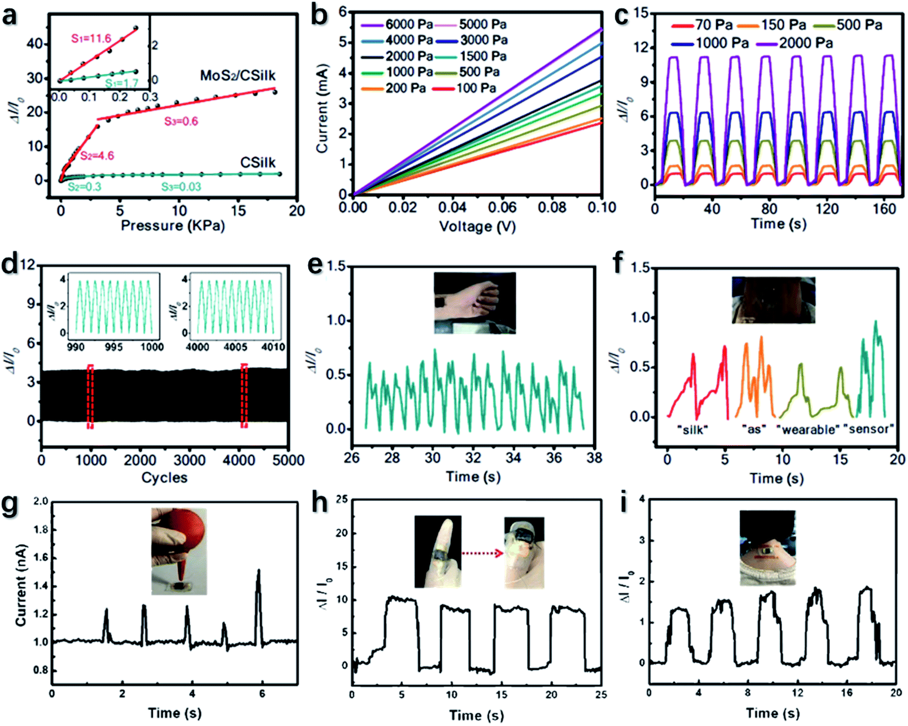 | ||
| Fig. 14 (a–f) The sensitivity, pressure-dependent V/I plot, short-term stability under various pressures, and long-term stability of the MoS2/CSilk sensor. Reproduced with permission from ref. 270, copyright 2020 ACS Applied Materials & Interfaces. (g–i) Multiple applications of TMD-based wearable sensors including pulse detection, talking sensing, gas flow detection, finger motion detection, and neck motion detection. Reproduced with permission from ref. 271, copyright 2020 Advanced Electronic Materials. | ||
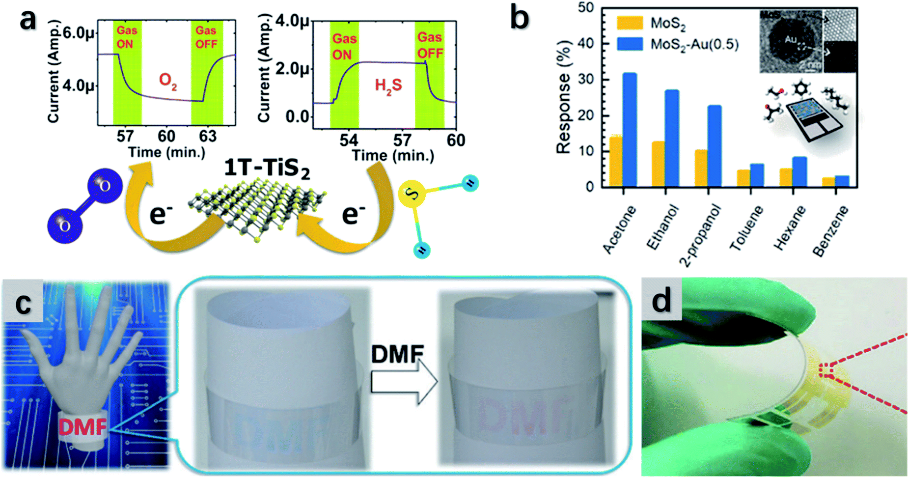 | ||
| Fig. 15 (a) The TiS2-based sensor which shows high sensitivity to O2 and H2S. Reproduced with permission from ref. 276, copyright 2020 ACS Applied Nano Materials. (b) The Au-doped MoS2 flexible gas sensor that shows strong responses towards versatile gases. Reproduced with permission from ref. 277, copyright 2019 ACS Applied Materials & Interfaces. (c) The wearable sensor composed of MoS2 exhibits color changes with exposure to DMF. Reproduced with permission from ref. 278, copyright 2017 Nanoscale. (d) Bendable MoSe2-based thin-film gas sensor for NH3 detection. Reproduced with permission from ref. 58, copyright 2019 Nano Energy. | ||
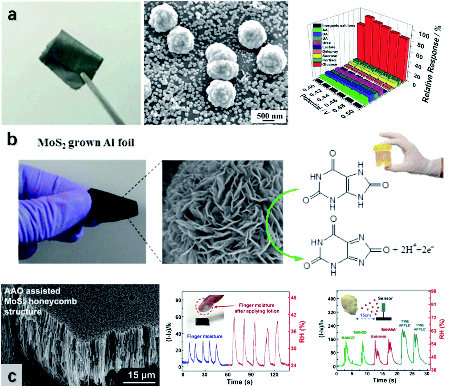 | ||
| Fig. 16 (a) The optical and SEM images of the GP/MoS2/Cu biosensor, showing its flexibility and microstructural morphology. The high sensitivity and selectivity of the sensor revealing its promising sensing performance. Reproduced with permission from ref. 282, copyright 2018 Analytical Biochemistry. (b) The flexible UA sensor composed of MoS2 nanoflowers and its mechanism for UA detection. Reproduced with permission from ref. 283, copyright 2019 Sensors and Actuators B: Chemical. (c) The moisture sensor with MoS2 honeycomb geometry, which delivers distinguishable signals towards fingers with and without hand lotion, and the breath-out air when people speak different words. Reproduced with permission from ref. 37, copyright 2020 ACS Applied Materials & Interfaces. | ||
4.4. Other applications
In the work of Barhoumi et al.,310 it is indicated that the bandgap of the MX2/M′X2 (X = Pt, Pd, W) heterostructure can be tuned in the range of 0.58 to 1.14 eV. Furthermore, fullerene/MX2 and silicene/MX2 hybrids have been found to have indirect bandgaps in the ranges of 1.02 to 1.62 eV and 0.89 to 1.62 eV, respectively, revealing their promising feasibility for photovoltaic applications. A flexible dye-sensitized solar cell has been developed with the flexible counter electrode prepared by a controlled electrodeposition of MoS2 thin films on the PET substrates.284 Ionic liquid electrolyte was utilized to modify the band level and enhance the device softness. The interfacial charge transfer of redox couples was accelerated at the MoS2 surface, leading to the enhanced rate of electron injection. As a result, the device delivered an improved current density of 12.46 mA cm−2 with the power conversion efficiency reaching 4.84%. In another work, a flexible perovskite photodiode/solar cell bifunctional device has been integrated with a hole transport layer built on MoS2/graphene heterostructures.285 The presence of MoS2 stabilized the perovskite/hole transport layer interface, and allowed the device to undergo continuous light soaking and 40% humidity for 100 h without degradation. The device exhibited a fast photoresponse and high linear dynamic range reaching 117 dB, indicating its excellent ability to detect light in a wide range of wavelengths. In the solar cell mode, the device showed a current density reaching 19.3 mA cm−2 and power efficiency reaching 12.0%. In terms of the durability, the bifunctional device can maintain 57% of the initial photocurrent over 3000 times of bending at 4 mm. MoSe2/WS2 hybrids have been employed as the counter electrode in the manufacture of a dye-sensitized solar cell.286 The hybrid interface showed rapid electron–hole relation and transport behavior. Hence, the solar cell provided a high photocurrent density of 23.1 mA cm−2 and power conversion efficiency of 9.92%. For a NiS2 nanoparticle-based solar cell, the charge transfer resistance was observed to be 3.8 Ω cm2 with a current density of 9.73 mA cm−2 and an efficiency of 4.55%.287 Owing to the superior photovoltaic properties and interfacial charge transport behaviors, TMDs have become promising candidates for flexible solar cells.288,289 However, they face challenges of chemical stability, transparency, and durability.290 Hence, continuous research to fully discover the application of TMDs in solar cells is expected to intensify.
Guo et al.299 improved the thermoelectric properties of MoS2 by p-type doping of Au. The presence of Au improves the electrical conductivity of 2H-MoS2 with a low percolation threshold. Besides, the local band shifts across the interface and filters the dopant-initiated carriers, which facilitates the decoupling of electrical conductivity and the Seebeck coefficient. As a result, the MoS2/Au hybrid exhibits promising p-type thermoelectric performances with the power factor reaching 166.3 μW m−1 K−2. Similarly, the 1T-WS2/SWCNT composite has been synthesized via the hydrothermal approach.300 The interfacial reactions between SWCNTs and WS2 crystals opened conductive paths and unlinked the electrical conductivity and Seebeck coefficient, leading to the promotion of both parameters simultaneously. The obtained power factor was 61.7 μW m−1 K−2. The decoration of CNTs onto MoS2 thin films can effectively increase the electrical conductivity and reduce the thermal conductivity.301 CNTs also have an influence on the shift of the Fermi level towards the valence band edge and increase the Seebeck coefficient. Hence, 20% doping of CNTs into MoS2 resulted in a ZT of 0.17. In addition, the hybrid film showed superior tensile stress, allowing it for wearable applications. Using body temperature as a heat source, the film provided a voltage output of 2.9 mV over 5 K. A unique facile electrochemical intercalation synthetic method has been proposed to fabricate a heterostructure with alternating inorganic TiS2 monolayers and organic cations.302 The organic cations act as electron stabilizers and allow for an n-type behaviour with a power factor of 0.45 mW m−1 K−2. The superlattice is favourable for phonon scattering and suppress the thermal conductivity. Besides, the intercalation of organic cations strongly increases the mechanical flexibility, as a flexural modulus of 145 MPa was found at 300 K. Owing a remarkable ZT of 0.28 and flexibility, the hybrid exhibited great potential for wearable TEG applications. In another work, hexylammonium TiS2 nanoparticles [TiS2(HA)x] were formulated into inks and directly printed on a flexible paper.303 It encouraged a new avenue not only for large-scale material synthesis, but also for flexible TEG fabrication. The device yielded a high degree of rolling and delivered a power density of 17.6 μW cm−2 at ΔT = 20 K.
5. Conclusions and perspectives
In this paper, TMD-based flexible electronics have been reviewed. Starting from the material, the structure, physical properties, and synthetic routes of TMDs have been introduced, and the feasibility of TMDs as promising candidates for flexible electronics has been discussed. Compared to bulk materials, monolayer and few-layer TMDs present different photoelectric properties due to the different charge transport mechanisms, including the opening of the bandgap and the indirect/direct bandgap transition. Besides, 2D materials also exhibit better flexibility and are suitable for printing, casting, screening, or even constructing 3D configurations. However, they are difficult to synthesize in large scales, which means they will take much more time and cost compared to commercial materials. Hence, it is suggested that multiple aspects should be considered when evaluating the materials used for flexible electronics, such as goal performances and efficiency, device scale, synthesis route, service environment, and relative budget. Compared to other 2D materials, TMDs have various compositions with versatile properties that are suitable for different fields. For instance, metallic 1T-TMDs are conductors, while semi-conducting 2H-TMDs are suitable for p-type electronics. Besides, the intrinsic large mechanical strength of TMDs allows them to be favorable for flexible electronics.Premised on these fundamental studies and future research direction, TMDs have become promising candidates for various flexible and wearable electronics. Nevertheless, there remain several challengeable issues to be addressed. (1) The first one is material synthesis and device fabrication. The realization of flexible electronics requires flexible substrates such as polymers, and the device thickness is usually at the micrometer scale. This brings challenges for the extensive production TMD thin films with high quality and the maintenance of device reproductivity. First, the polymer substrate can only sustain low synthetic temperature. However the CVD approach is universal for most TMD systems and can prepare large-scale TMD nanomaterials. However, the preparation procedure requires high temperature, which limits the deposition of TMDs on polymer substrates. Second, the mechanical exfoliation has advantages of easy processing, low synthetic temperature, and low cost, but the thickness and homogeneity are difficult to control. Third, other researchers explored some approaches to directly grow TMDs on flexible substrates by plasma, magnetron sputtering, and laser beam methods. These techniques can realize the crystallization of TMDs on flexible substrates with low damage fabrication. Nevertheless, they are not appropriate for extensive manufacturing. Fourth, TMD films can also be transferred onto substrates; however, the process may involve chemical etching that degrades the quality of TMD films. Besides, the separation of the TMD/polymer multilayer may cause damages to the TMD surface, leading to an unstable subsequent substrate growth. Furthermore, the defects on TMDs trap charges and increase the SBH, causing declined device performances. Due to the disadvantage of the aforementioned methods, large-scale, controllable, universal, damage-free, low cost, and low-temperature synthetic routes towards high densification and quality TMD films are urgently needed. (2) For an integrated device, though 2D TMDs exhibit promising properties, the contact resistance at the interface may limit the device performance. Hence, they require optimized electrical and mechanical contact interfaces. The contact resistance can be caused by defects in materials, impurities, surface roughness, and so on. Hence, further research studies should aim at improving the TMD crystallization, surface roughness, and modifying the Fermi level. (3) Further improvements of TMD devices' flexibility and stretchability are urgent. Some devices contain brittle functional layers, such as HfO2 dielectrics or Al2O3 encapsulation layers. Though the flexibility of these materials can be improved by reducing the thickness, it is still challenging to improve their stretchability. The lack of stretchability may lead to mechanical failure of the device from the inside or in an even worse case, the device is detached from the human skin. Hence, continuous research studies are needed to improve the integrated device stretchability and maintain a reliable device adhesion to the human skin. (4) An additional challenge is the incomplete understanding of the inherent electronic/photonic conducting mechanisms and chemical behaviors of TMDs. In-depth studies are required to explore the fundamental theories that can explain the relationship among material band structures, crystal microstructures, material properties, and device performance. The knowledge is beneficial for promoting the device performance and slowing down the device degradation. For instance, 1T-TMDs are unstable and transform back to 2H phases at room temperature. Hence, the transformation mechanism is needed to investigate to find solutions to stabilize 1T-TMDs and the crystalline engineering of TMDs needs further exploration. (5) The realization of integrated functional devices and the exploration of new applications are necessary. TMD-based AIB anodes have been intensively developed, but the integration of full flexible batteries is challenging. The issues include the realization of the entire flexible anode/electrolyte/cathode system, the prevention of charge leakages, electrochemical improvements of full batteries, etc. TMD-biosensors are at a preliminary stage as the related interaction mechanisms require in-depth studies. Besides, the development of body-implant TMD-biosensors is quite blank, and is urgent for exploration. (6) Finally, the full exploration of the TMD family in flexible applications is eagerly needed. The different combinations of transition metal and dichalcogenide atoms allow for manifold TMD compositions. However, the most frequently used TMDs for current flexible electronics and batteries are Mo- and W-based materials. And for flexible biosensors, the material selection is even more limited, as TMDs beyond MoS2 have barely been applied to such applications. Other TMDs such as XS2 (X = Ni, Pd, Pt) have comparable band structures to Mo- and W-based TMDs, and exhibit semiconducting/metallic transfer upon external stress. Hence, they are excellent candidates for flexible photoelectric or electronic devices.304 PtS2 and WSe2 exhibit superior photoelectrochemical performances and are feasible for photoelectric devices,305 while PtX2 (X = S, Se, Te) may become promising thermoelectric materials as they present an outstanding calculated ZT over 2 at room temperature.306 However, these materials have attracted much less attention than MoS2. Therefore, it is of great potential to explore new TMD materials for different flexible devices.
For future research of TMD-based flexible applications, several predictions have been proposed. (1) In terms of the development of advanced device fabrication, electrochemical methods in the aqueous environment may attract more interest. The low reaction temperature is beneficial for the integration of polymer substrates, and the soluble products can be used as ink for large-scale printing. Other advanced synthetic techniques that accept low-temperature synthesis of high-quality TMD thin films will be highlighted, such as the ALD method and aerosol deposition method.307 (2) Advanced device architectures with superior stretchability will be developed to introduce flexibility into the rigid component of TMD-based devices. The “island and bridge”,308 wavy33 and honeycomb39 architectures are suitable for manufacturing rigid inorganic stretchable electronics. The “island and bridge” hybrid is suitable for rigid materials and withstands multidirectional strain, which results in a broad variety of applications. However, the fabrication of micro-size islands can be complicated and costly. The synthetic processing of the wavy structure is relatively easy, though it requires multiple steps indeed. Therefore, it shows potential in the large-scale manufacture of stretchable electronics. However, the wavy structure withstands linear strain only, which limits its applications. Researchers should choose the most suitable device configuration according to the specific uses of the devices. (3) The research on device efficiency enhancements will continue. For TFTs, strategies for reducing the contact resistance and improving TMD mobility are highly required. It is suggested that a crested design with great surface roughness is favorable for carrier mobility enhancement.207 Therefore, it is possible to combine the crested design with the wavy configuration to improve both device mobility and stretchability. For energy storage and sensing applications, the specific area takes a leading role in maximizing the lithium-ion capacity. Hence, 0D and 1D materials, and architectures with porous, lamellar, and hollow geometries are preferred for the fabrication of electrodes. Besides, owing to the addition of active sites and enhanced electronic conductivity, hybrid electrodes, especially the TMD/graphene composites, exhibit promising electrochemical performances and will be continuously developed. Numerous studies have been published on TMD flexible sensors, however, most of which are MoS2-based. Hence, the exploration of other TMDs (beyond MoS2) needs further investigation. Janus TMDs (MXY, X ≠ Y) have layered structures with similar electrical and mechanical properties as the normal TMDs.309 Moreover, they also present strong piezoelectric properties, which are suitable for motion sensor applications. Other challenges for wearable TMD sensors include enhancing the stretchability, minimizing the contact resistance between the human body and the device, improving response/recovery time for real-time sensing, and maintaining the device stability in human body environments. (4) Though TMDs have proved their excellent feasibility in various flexible applications, the exploration of other immature and new areas will be carried out. Flexible displays, flexible antennas, body-implant bio-devices, wearable thermoelectric generators, etc. will attract more interest.
Though challenges in practical use and industrial production of flexible devices based on TMDs still exist, it should be highlighted that more achievements will be obtained with continuous research. TMDs are proved to be outstanding materials for flexible applications in the field of energy storage, smart electronics, human health care, military, and space exploration (Fig. 17).
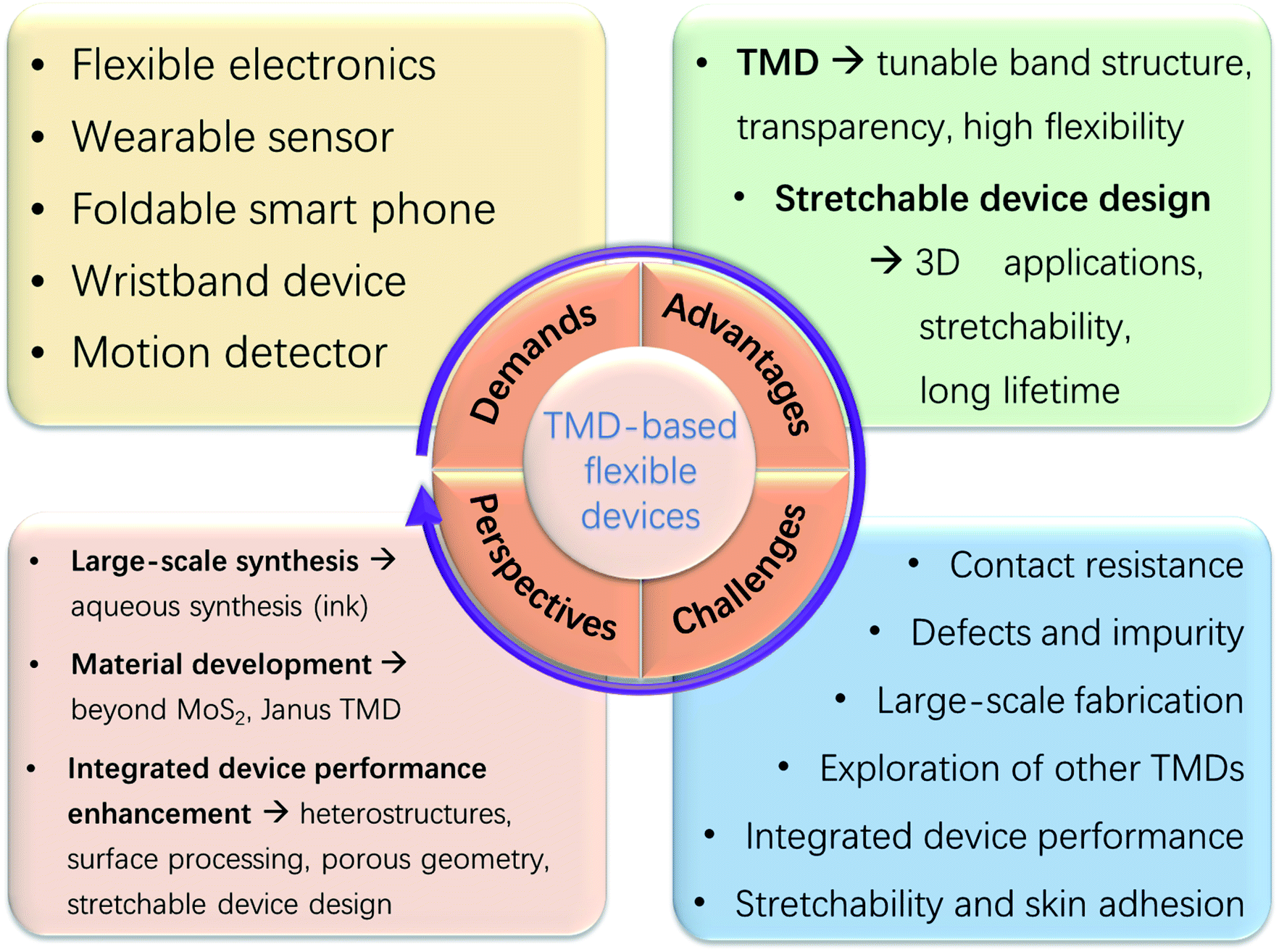 | ||
| Fig. 17 Summaries, challenges, and future perspectives of 2D TMD-based flexible devices. | ||
Abbreviations
| 2D | 2-Dimensional |
| AAO | Anodic aluminum oxide |
| AIB | Alkali metal-ion battery |
| ALD | Atomic-layer deposition |
| APCVD | Ambient-pressure chemical vapor deposition |
| ASC | Asymmetric supercapacitor |
| BP | Black phosphorus |
| CC | Carbon cloth |
| CF | Carbon fiber |
| CFC | Carbon fiber cloth |
| CHP | Cyclohexylpyrrolidone |
| CNF | Carbon nanofiber |
| CNT | Carbon nanotube |
| CSilk | Carbonized silk |
| CVD | Chemical vapor deposition |
| DC | Direct current |
| DDP | Diketopyrrolopyrrole |
| DFT | Density functional theory |
| DHF | Diluted hydrofluoric acid |
| DMF | N,N-Dimethylformamide |
| DT | Diamond-chain |
| E-BFC | Electronic-skin-based biofuel cell |
| EQE | External quantum efficiency |
| FET | Field-effect transistor |
| GO | Graphene oxide |
| gp120 | Envelope glycoprotein GP120 |
| HCVD | Horizontal chemical vapor deposition |
| H-CVD | Hydrogen-controlled chemical vapor deposition |
| HER | Hydrogen evolution reaction |
| HPCF | Polyacrylonitrile carbon nanofiber |
| ICE | Initial coulombic efficiency |
| iCVD | Initiated chemical vapor deposition |
| ITO | Tin doped indium oxide |
| JEFT | Junction field-effect transistor |
| LIB | Lithium-ion battery |
| LOD | Lactate oxidase |
| MMT | Montmorillonite |
| MOCVD | Metalorganic chemical vapor deposition |
| MSC | Microsupercapacitor |
| MXene | Transition metal carbide and nitride |
| NCMT | N-doped carbon microtube |
| NGQD | Nitrogen-doped graphene quantum dot |
| NMP | N-Methylpyrrolidone |
| OA | Oleic acid |
| OCNTF | Oxidized carbon nanotube fiber |
| OLED | Organic light-emitting diode |
| p(V4D4-co-CHMA) | Poly(2,4,6,8-tetramethyl-2,4,6,8-tetravinylcyclotetrasiloxane-co-cyclohexyl methacrylate) |
| PANI | Polyaniline |
| PCC | Porous carbon cloth |
| PCF | Porous carbon fiber |
| PCNF | Porous carbon nanofiber |
| PDA | Polydiacetylene |
| PDMS | Poly-dimethylsiloxane |
| PECVD | Plasma-enhanced chemical vapor deposition |
| PEDOT | Poly-3,4-ethylenedioxythiophene |
| PEN | Polyethylene naphthalate |
| PET | Polyethylene terephthalate |
| PI | Polyimide |
| PMMA | Poly-methylmethacrylate |
| PPy | Polypyrrole |
| PS-NH2 | Amine-terminated polystyrene |
| PSS | Polystyrene sulfonate |
| RGO | Reduced graphene oxide |
| SBA-15 | Santa Barbara Amorphous-15 |
| SBH | Schottky barrier height |
| SEI | Solid-electrolyte interface |
| SEM | Scanning electron microscope |
| SS | Subthreshold swing |
| SWCNT | Single wall carbon nanotube |
| TEG | Thermoelectric generator |
| TEM | Transmission electron microscope |
| TFT | Thin-film transistor |
| TMC | Transition metal chalcogenide |
| TMD | Transition metal dichalcogenide |
| TMO | Transition metal oxide |
| UA | Uric acid |
| UHV | Ultra-high vacuum |
| VBM | Valence band maximum |
| VCVD | Vertical chemical vapor deposition |
| vdW | van der Waals |
| VOC | Volatile organic compounds |
| ZIO | Zinc indium oxide |
| ZTO | Zinc tin oxide |
Conflicts of interest
There are no conflicts to declare.Acknowledgements
This research was supported by the Science and Technology Innovation Commission of Shenzhen (JCYJ20180507181858539 and JCYJ20190808173815205), National Natural Science Foundation of China (51804199), Guangdong Basic and Applied Basic Research Foundation (2019A1515012111), Shenzhen Science and Technology Program (KQTD20180412181422399), and the National Key R&D Program of China (2019YFB2204500).References
- G. Gustafsson, Y. Cao, G. M. Treacy, F. Klavetter, N. Colaneri and A. J. Heeger, Nature, 1992, 357, 477–479 CrossRef CAS.
- A. Nadarajah, R. C. Word, J. Meiss and R. Könenkamp, Nano Lett., 2008, 8, 534–537 CrossRef CAS PubMed.
- L. Martínez-Sarti, A. Pertegás, M. Monrabal-Capilla, E. Gilshteyn, I. Varjos, E. I. Kauppinen, A. G. Nasibulin, M. Sessolo and H. J. Bolink, Org. Electron., 2016, 30, 36–39 CrossRef.
- D. Ji, L. Jiang, X. Cai, H. Dong, Q. Meng, G. Tian, D. Wu, J. Li and W. Hu, Org. Electron., 2013, 14, 2528–2533 CrossRef CAS.
- J.-H. Kim, S. Yun, H.-U. Ko and J. Kim, Curr. Appl. Phys., 2013, 13, 897–901 CrossRef.
- B. Lahey, A. Girouard, W. Burleson and R. Vertegaal, in Proceedings of the 2011 Annual Conference on Human Factors in Computing Systems – CHI '11, ACM Press, New York, USA, 2011, p. 1303 Search PubMed.
- H. Edzer, A. Huitema, G. H. Gelinck, P. J. Van Lieshout, F. J. Van Veenendaal and E. Touwslager, J. Soc. Inf. Disp., 2006, 14, 729–733 CrossRef.
- K. Xiong, G. Emilsson, A. Maziz, X. Yang, L. Shao, E. W. H. Jager and A. B. Dahlin, Adv. Mater., 2016, 28, 9956–9960 CrossRef CAS PubMed.
- D. H. Shin, J. H. Heo and S. H. Im, J. Korean Phys. Soc., 2017, 71, 593–607 CrossRef.
- R. Wang, X. Dai, Z. Qian, Y. Sun, S. Fan, K. Xiong, H. Zhang and F. Wu, ACS Mater. Lett., 2020, 2, 280–290 CrossRef CAS.
- T. Li, Y. Li, Y. Sun, Z. Qian and R. Wang, ACS Mater. Lett., 2021, 3, 838–844 CrossRef CAS.
- Y. Pang, Z. Yang, Y. Yang and T. Ren, Small, 2020, 16, 1901124 CrossRef CAS PubMed.
- R. L. Crabb and F. C. Treble, Nature, 1967, 213, 1223–1224 CrossRef.
- A. Nathan, A. Ahnood, M. T. Cole, S. Lee, Y. Suzuki, P. Hiralal, F. Bonaccorso, T. Hasan, L. Garcia-Gancedo, A. Dyadyusha, S. Haque, P. Andrew, S. Hofmann, J. Moultrie, D. Chu, A. J. Flewitt, A. C. Ferrari, M. J. Kelly, J. Robertson, G. A. J. Amaratunga and W. I. Milne, Proc. IEEE, 2012, 100, 1486–1517 Search PubMed.
- W. S. Wong, E. Alberto Salleo and A. Salleo, Flexible Electronics, Springer US, Boston, MA, 2009, vol. 11 Search PubMed.
- K. F. Mak, C. Lee, J. Hone, J. Shan and T. F. Heinz, Phys. Rev. Lett., 2010, 105, 136805 CrossRef PubMed.
- A. Roy, H. C. P. Movva, B. Satpati, K. Kim, R. Dey, A. Rai, T. Pramanik, S. Guchhait, E. Tutuc and S. K. Banerjee, ACS Appl. Mater. Interfaces, 2016, 8, 7396–7402 CrossRef CAS PubMed.
- H.-L. Liu, C.-C. Shen, S.-H. Su, C.-L. Hsu, M.-Y. Li and L.-J. Li, Appl. Phys. Lett., 2014, 105, 201905 CrossRef.
- S. Deng, L. Li and M. Li, Phys. E, 2018, 101, 44–49 CrossRef CAS.
- K. S. Novoselov, D. Jiang, F. Schedin, T. J. Booth, V. V. Khotkevich, S. V. Morozov and A. K. Geim, Proc. Natl. Acad. Sci. U. S. A., 2005, 102, 10451–10453 CrossRef CAS PubMed.
- R. B. Bergmann, C. Berge, T. J. Rinke and J. H. Werner, Mater. Res. Soc. Symp. Proc., 2001, 685, 11–16 CrossRef.
- Y. Lee, S. Bae, H. Jang, S. Jang, S. E. Zhu, S. H. Sim, Y. Il Song, B. H. Hong and J. H. Ahn, Nano Lett., 2010, 10, 490–493 CrossRef CAS.
- D. Song, A. Mahajan, E. B. Secor, M. C. Hersam, L. F. Francis and C. D. Frisbie, ACS Nano, 2017, 11, 7431–7439 CrossRef CAS PubMed.
- W. S. Wong and A. Salleo, Flexible Electronics: Materials and Applications, 2009 Search PubMed.
- Y. Y. Kim, T. Yang, R. Suhonen, M. Välimäki, T. Maaninen, A. Kemppainen, N. J. Jeon and J. Seo, Adv. Sci., 2019, 6, 1802094 CrossRef PubMed.
- J. R. Corea, A. M. Flynn, B. Lechêne, G. Scott, G. D. Reed, P. J. Shin, M. Lustig and A. C. Arias, Nat. Commun., 2016, 7, 10839 CrossRef CAS PubMed.
- Y. Wang, Y.-Z. Zhang, D. Dubbink and J. E. ten Elshof, Nano Energy, 2018, 49, 481–488 CrossRef CAS.
- M. G. Mohammed and R. Kramer, Adv. Mater., 2017, 29, 1604965 CrossRef PubMed.
- W. Wu, Sci. Technol. Adv. Mater., 2019, 20, 187–224 CrossRef CAS.
- N. Matsuhisa, X. Chen, Z. Bao and T. Someya, Chem. Soc. Rev., 2019, 48, 2946–2966 RSC.
- T. Dinh, T. Nguyen, H. Phan, T. Nguyen, V. T. Dau, N. Nguyen and D. V. Dao, Small, 2020, 16, 1905707 CrossRef CAS.
- S. P. Lacour, J. Jones, S. Wagner, T. Li and Z. Suo, Proc. IEEE, 2005, 93, 1459–1467 CAS.
- J. Nam, B. Seo, Y. Lee, D. Kim and S. Jo, Sci. Rep., 2017, 7, 7575 CrossRef.
- A. Takei, S. Tsukamoto, Y. Komazaki, Y. Kusaka, K. Kuribara and M. Yoshida, AIP Adv., 2020, 10, 025205 CrossRef.
- J. Zhou, X. Xu, Y. Xin and G. Lubineau, Adv. Funct. Mater., 2018, 28, 1–8 Search PubMed.
- T. Q. Trung, H. S. Le, T. M. L. Dang, S. Ju, S. Y. Park and N.-E. Lee, Adv. Healthcare Mater., 2018, 7, 1800074 CrossRef PubMed.
- S. Mondal, S. J. Kim and C.-G. Choi, ACS Appl. Mater. Interfaces, 2020, 12, 17029–17038 CrossRef CAS PubMed.
- Z. Lv, Y. Tang, Z. Zhu, J. Wei, W. Li, H. Xia, Y. Jiang, Z. Liu, Y. Luo, X. Ge, Y. Zhang, R. Wang, W. Zhang, X. J. Loh and X. Chen, Adv. Mater., 2018, 30, 1805468 CrossRef.
- S. Kang, S. Y. Hong, N. Kim, J. Oh, M. Park, K. Y. Chung, S.-S. Lee, J. Lee and J. G. Son, ACS Nano, 2020, 14, 3660–3668 CrossRef CAS PubMed.
- D. B. Mitzi, L. L. Kosbar, C. E. Murray, M. Copel and A. Afzali, Nature, 2004, 428, 299–303 CrossRef CAS PubMed.
- H. E. Unalan, Y. Yang, Y. Zhang, P. Hiralal, D. Kuo, S. Dalal, T. Butler, S. N. Cha, J. E. Jang, K. Chremmou, G. Lentaris, D. Wei, R. Rosentsveig, K. Suzuki, H. Matsumoto, M. Minagawa, Y. Hayashi, M. Chhowalla, A. Tanioka, W. I. Milne, R. Tenne and G. A. J. Amaratunga, IEEE Trans. Electron Devices, 2008, 55, 2988–3000 CAS.
- D. Jariwala, V. K. Sangwan, L. J. Lauhon, T. J. Marks and M. C. Hersam, ACS Nano, 2014, 8, 1102–1120 CrossRef CAS.
- Z. Lei, W. Zhu, S. Sun and P. Wu, Nanoscale, 2016, 8, 18800–18807 RSC.
- B. Radisavljevic, A. Radenovic, J. Brivio, V. Giacometti and A. Kis, Nat. Nanotechnol., 2011, 6, 147–150 CrossRef CAS PubMed.
- E. Singh, P. Singh, K. S. Kim, G. Y. Yeom and H. S. Nalwa, ACS Appl. Mater. Interfaces, 2019, 11, 11061–11105 CrossRef CAS PubMed.
- Y. Woo, W. Hong, S. Y. Yang, H. J. Kim, J. Cha, J. E. Lee, K. J. Lee, T. Kang and S. Choi, Adv. Electron. Mater., 2018, 4, 1800251 CrossRef.
- X. Xu, L. Wu, Y. Sun, T. Wang, X. Chen, Y. Wang, W. Zhong and Y. Du, J. Electroanal. Chem., 2018, 811, 96–104 CrossRef CAS.
- D. Li, W. Zhou, Q. Zhou, G. Ye, T. Wang, J. Wu, Y. Chang and J. Xu, Nanotechnology, 2017, 28, 395401 CrossRef.
- S. Mukherjee, J. Turnley, E. Mansfield, J. Holm, D. Soares, L. David and G. Singh, R. Soc. Open Sci., 2019, 6, 190437 CrossRef CAS PubMed.
- Y. Li, R. Wang, Z. Guo, Z. Xiao, H. Wang, X. Luo and H. Zhang, J. Mater. Chem. A, 2019, 7, 25227–25246 RSC.
- M. Park, Y. J. Park, X. Chen, Y. Park, M. Kim and J.-H. Ahn, Adv. Mater., 2016, 28, 2556–2562 CrossRef CAS PubMed.
- C. Choi, Y. Lee, K. W. Cho, J. H. Koo and D. Kim, Acc. Chem. Res., 2019, 52, 73–81 CrossRef CAS.
- A. Sinha, Dhanjai, B. Tan, Y. Huang, H. Zhao, X. Dang, J. Chen and R. Jain, TrAC, Trends Anal. Chem., 2018, 102, 75–90 CrossRef CAS.
- A. Chhetry, M. Sharifuzzaman, H. Yoon, S. Sharma, X. Xuan and J. Y. Park, ACS Appl. Mater. Interfaces, 2019, 11, 22531–22542 CrossRef CAS PubMed.
- J. Jang, H. Kim, S. Ji, H. J. Kim, M. S. Kang, T. S. Kim, J. E. Won, J. H. Lee, J. Cheon, K. Kang, W. Bin Im and J. U. Park, Nano Lett., 2020, 20, 66–74 CrossRef CAS PubMed.
- X. Zhang, J. Grajal, J. L. Vazquez-Roy, U. Radhakrishna, X. Wang, W. Chern, L. Zhou, Y. Lin, P. C. Shen, X. Ji, X. Ling, A. Zubair, Y. Zhang, H. Wang, M. Dubey, J. Kong, M. Dresselhaus and T. Palacios, Nature, 2019, 566, 368–372 CrossRef PubMed.
- S. M. Shinde, T. Das, A. T. Hoang, B. K. Sharma, X. Chen and J.-H. Ahn, Adv. Funct. Mater., 2018, 28, 1706231 CrossRef.
- D. Zhang, Z. Yang, P. Li, M. Pang and Q. Xue, Nano Energy, 2019, 65, 103974 CrossRef CAS.
- M. Choi, Y. J. Park, B. K. Sharma, S.-R. Bae, S. Y. Kim and J.-H. Ahn, Sci. Adv., 2018, 4, eaas8721 CrossRef PubMed.
- X. Lin, D. Xue, L. Zhao, F. Zong, X. Duan, X. Pan, J. Zhang and Q. Li, Chem. Eng. J., 2019, 356, 483–491 CrossRef CAS.
- V. Rana, P. Gangwar, J. S. Meena, A. K. Ramesh, K. N. Bhat, S. Das and P. Singh, Nanotechnology, 2020, 31, 385501 CrossRef CAS PubMed.
- Y. Wang, D. Kong, S. Huang, Y. Shi, M. Ding, Y. Von Lim, T. Xu, F. Chen, X. Li and H. Y. Yang, J. Mater. Chem. A, 2018, 6, 10813–10824 RSC.
- J.-H. Ahn and B. H. Hong, Nat. Nanotechnol., 2014, 9, 737–738 CrossRef PubMed.
- P. F. Carcia, R. S. McLean, M. H. Reilly, I. Malajovich, K. G. Sharp, S. Agrawal and G. Nunes, MRS Proc., 2003, 769, H7.2 CrossRef.
- D. Hong and J. F. Wager, J. Vac. Sci. Technol., B: Microelectron. Nanometer Struct., 2005, 23, L25 CrossRef CAS.
- S.-J. Seo, C. G. Choi, Y. H. Hwang and B.-S. Bae, J. Phys. D: Appl. Phys., 2009, 42, 035106 CrossRef.
- W. B. Jackson, G. S. Herman, R. L. Hoffman, C. Taussig, S. Braymen, F. Jeffery and J. Hauschildt, J. Non-Cryst. Solids, 2006, 352, 1753–1755 CrossRef CAS.
- K. S. Novoselov, A. K. Geim, S. V. Morozov, D. Jiang, Y. Zhang, S. V. Dubonos, I. V. Grigorieva and A. A. Firsov, Science, 2004, 306, 666–669 CrossRef CAS PubMed.
- Y. L. Huang, W. Chen and A. T. S. Wee, SmartMat, 2021, 2, 139–153 CrossRef.
- E. Senokos, V. Reguero, L. Cabana, J. Palma, R. Marcilla and J. J. Vilatela, Adv. Mater. Technol., 2017, 2, 1600290 CrossRef.
- Y. Liu, G. Li, Y. Guo, Y. Ying and X. Peng, ACS Appl. Mater. Interfaces, 2017, 9, 14043–14050 CrossRef CAS PubMed.
- D. Zhang, K. Ryu, X. Liu, E. Polikarpov, J. Ly, M. E. Tompson and C. Zhou, Nano Lett., 2006, 6, 1880–1886 CrossRef CAS PubMed.
- R. Bandyopadhyaya, E. Nativ-Roth, O. Regev and R. Yerushalmi-Rozen, Nano Lett., 2002, 2, 25–28 CrossRef CAS.
- J. Yu, N. Grossiord, C. E. Koning and J. Loos, Carbon, 2007, 45, 618–623 CrossRef CAS.
- A. K. Geim and K. S. Novoselov, Nat. Mater., 2007, 6, 183–191 CrossRef CAS PubMed.
- G. Eda, C. Mattevi, H. Yamaguchi, H. Kim and M. Chhowalla, J. Phys. Chem. C, 2009, 113, 15768–15771 CrossRef CAS.
- J. Kim, L. J. Cote and J. Huang, Acc. Chem. Res., 2012, 45, 1356–1364 CrossRef CAS PubMed.
- S. Pei, J. Zhao, J. Du, W. Ren and H.-M. Cheng, Carbon, 2010, 48, 4466–4474 CrossRef CAS.
- I. Jung, D. A. Dikin, R. D. Piner and R. S. Ruoff, Nano Lett., 2008, 8, 4283–4287 CrossRef CAS PubMed.
- J. Qiao, X. Kong, Z.-X. Hu, F. Yang and W. Ji, Nat. Commun., 2014, 5, 4475 CrossRef CAS PubMed.
- L. Li, Y. Yu, G. J. Ye, Q. Ge, X. Ou, H. Wu, D. Feng, X. H. Chen and Y. Zhang, Nat. Nanotechnol., 2014, 9, 372–377 CrossRef CAS PubMed.
- S. Luo, J. Zhao, J. Zou, Z. He, C. Xu, F. Liu, Y. Huang, L. Dong, L. Wang and H. Zhang, ACS Appl. Mater. Interfaces, 2018, 10, 3538–3548 CrossRef CAS PubMed.
- F. Shi, K. Huang and S. Feng, ChemCatChem, 2020, 12, 1913–1921 CrossRef CAS.
- C. Hu, Q. Xiao, Y. Ren, M. Zhao, G. Dun, H. Wu, X. Li, Q. Yang, B. Sun, Y. Peng, F. Yan, Q. Wang and H.-L. Zhang, Adv. Funct. Mater., 2018, 28, 1805311 CrossRef.
- B. Peng, H. Zhang, H. Shao, Y. Xu, R. Zhang and H. Zhu, J. Mater. Chem. C, 2016, 4, 3592–3598 RSC.
- Y. Liu, Y.-J. Dong, Z. Tang, X.-F. Wang, L. Wang, T. Hou, H. Lin and Y. Li, J. Mater. Chem. C, 2016, 4, 6380–6385 RSC.
- T. Cheng, H. Lang, Z. Li, Z. Liu and Z. Liu, Phys. Chem. Chem. Phys., 2017, 19, 23942–23950 RSC.
- A. J. Mannix, X.-F. Zhou, B. Kiraly, J. D. Wood, D. Alducin, B. D. Myers, X. Liu, B. L. Fisher, U. Santiago, J. R. Guest, M. J. Yacaman, A. Ponce, A. R. Oganov, M. C. Hersam and N. P. Guisinger, Science, 2015, 350, 1513–1516 CrossRef CAS PubMed.
- H. Wang, Q. Li, Y. Gao, F. Miao, X.-F. Zhou and X. G. Wan, New J. Phys., 2016, 18, 073016 CrossRef.
- Q. Wu, S. Chen, Y. Wang, L. Wu, X. Jiang, F. Zhang, X. Jin, Q. Jiang, Z. Zheng, J. Li, M. Zhang and H. Zhang, Adv. Mater. Technol., 2019, 4, 1800532 CrossRef.
- M. Khazaei, M. Arai, T. Sasaki, C.-Y. Chung, N. S. Venkataramanan, M. Estili, Y. Sakka and Y. Kawazoe, Adv. Funct. Mater., 2013, 23, 2185–2192 CrossRef CAS.
- X. Zhang, X. Zhao, D. Wu, Y. Jing and Z. Zhou, Nanoscale, 2015, 7, 16020–16025 RSC.
- Y. Xiao, M. Zhou, J. Liu, J. Xu and L. Fu, Sci. China Mater., 2019, 62, 759–775 CrossRef CAS.
- J. Zhou, J. Lin, X. Huang, Y. Zhou, Y. Chen, J. Xia, H. Wang, Y. Xie, H. Yu, J. Lei, D. Wu, F. Liu, Q. Fu, Q. Zeng, C.-H. Hsu, C. Yang, L. Lu, T. Yu, Z. Shen, H. Lin, B. I. Yakobson, Q. Liu, K. Suenaga, G. Liu and Z. Liu, Nature, 2018, 556, 355–359 CrossRef CAS PubMed.
- D. Voiry, A. Mohite and M. Chhowalla, Chem. Soc. Rev., 2015, 44, 2702–2712 RSC.
- S. Ahmad and S. Mukherjee, Graphene, 2014, 03, 52–59 CrossRef.
- J. E. Padilha, H. Peelaers, A. Janotti and C. G. Van de Walle, Phys. Rev. B: Condens. Matter Mater. Phys., 2014, 90, 205420 CrossRef.
- Q. H. Wang, K. Kalantar-Zadeh, A. Kis, J. N. Coleman and M. S. Strano, Nat. Nanotechnol., 2012, 7, 699–712 CrossRef CAS PubMed.
- S. Manzeli, D. Ovchinnikov, D. Pasquier, O. V. Yazyev and A. Kis, Nat. Rev. Mater., 2017, 2, 17033 CrossRef CAS.
- H. M. Hill, A. F. Rigosi, K. T. Rim, G. W. Flynn and T. F. Heinz, Nano Lett., 2016, 16, 4831–4837 CrossRef CAS PubMed.
- A. Splendiani, L. Sun, Y. Zhang, T. Li, J. Kim, C.-Y. Chim, G. Galli and F. Wang, Nano Lett., 2010, 10, 1271–1275 CrossRef CAS PubMed.
- T. Boeker, R. Severin, A. Mueller, C. Janowitz, R. Manzke, D. Voss, P. Krueger, A. Mazur and J. Pollmann, Phys. Rev. B: Condens. Matter Mater. Phys., 2001, 64, 235305 CrossRef.
- A. Kumar and P. K. Ahluwalia, Eur. Phys. J. B, 2012, 85, 186 CrossRef.
- P. a. Bertrand, Phys. Rev. B: Condens. Matter Mater. Phys., 1991, 44, 5745–5749 CrossRef CAS PubMed.
- H. Li, Q. Zhang, C. C. R. Yap, B. K. Tay, T. H. T. Edwin, A. Olivier and D. Baillargeat, Adv. Funct. Mater., 2012, 22, 1385–1390 CrossRef CAS.
- X. Huang, Z. Zeng and H. Zhang, Chem. Soc. Rev., 2013, 42, 1934 RSC.
- F. Wu, T. Lovorn and A. H. MacDonald, Phys. Rev. B, 2018, 97, 035306 CrossRef CAS.
- C. Robert, M. A. Semina, F. Cadiz, M. Manca, E. Courtade, T. Taniguchi, K. Watanabe, H. Cai, S. Tongay, B. Lassagne, P. Renucci, T. Amand, X. Marie, M. M. Glazov and B. Urbaszek, Phys. Rev. Mater., 2018, 2, 011001 CrossRef CAS.
- A. Molina-Sánchez, M. Palummo, A. Marini and L. Wirtz, Phys. Rev. B, 2016, 93, 155435 CrossRef.
- Z. Li, Y. Li, T. Han, X. Wang, Y. Yu, B. Tay, Z. Liu and Z. Fang, ACS Nano, 2017, 11, 1165–1171 CrossRef CAS PubMed.
- A. K. M. Newaz, D. Prasai, J. I. Ziegler, D. Caudel, S. Robinson, R. F. Haglund Jr and K. I. Bolotin, Solid State Commun., 2013, 155, 49–52 CrossRef CAS.
- C. Yim, M. O'Brien, N. McEvoy, S. Winters, I. Mirza, J. G. Lunney and G. S. Duesberg, Appl. Phys. Lett., 2014, 104, 103114 CrossRef.
- Z. Y. Zhu, Y. C. Cheng and U. Schwingenschlögl, Phys. Rev. B: Condens. Matter Mater. Phys., 2011, 84, 153402 CrossRef.
- Y. Niu, S. Gonzalez-Abad, R. Frisenda, P. Marauhn, M. Drüppel, P. Gant, R. Schmidt, N. Taghavi, D. Barcons, A. Molina-Mendoza, S. de Vasconcellos, R. Bratschitsch, D. Perez De Lara, M. Rohlfing and A. Castellanos-Gomez, Nanomaterials, 2018, 8, 725 CrossRef PubMed.
- A. Castellanos-Gomez, J. Quereda, H. P. van der Meulen, N. Agraït and G. Rubio-Bollinger, Nanotechnology, 2016, 27, 115705 CrossRef PubMed.
- C. Lee, X. Wei, J. W. Kysar and J. Hone, Science, 2008, 321, 385–388 CrossRef CAS PubMed.
- J.-W. Jiang, J.-S. Wang and B. Li, Phys. Rev. B: Condens. Matter Mater. Phys., 2009, 80, 113405 CrossRef.
- S. Bertolazzi, J. Brivio and A. Kis, ACS Nano, 2011, 5, 9703–9709 CrossRef CAS PubMed.
- J. L. Feldman, J. Phys. Chem. Solids, 1976, 37, 1141–1144 CrossRef CAS.
- A. Castellanos-Gomez, M. Poot, G. A. Steele, H. S. J. van der Zant, N. Agraït and G. Rubio-Bollinger, Adv. Mater., 2012, 24, 772–775 CrossRef CAS PubMed.
- Q. Xiong, N. Duarte, S. Tadigadapa and P. C. Eklund, Nano Lett., 2006, 6, 1904–1909 CrossRef CAS PubMed.
- S. Xiong and G. Cao, Nanotechnology, 2015, 26, 185705 CrossRef PubMed.
- J. Kang, H. Sahin and F. M. Peeters, Phys. Chem. Chem. Phys., 2015, 17, 27742–27749 RSC.
- J. P. Oviedo, S. KC, N. Lu, J. Wang, K. Cho, R. M. Wallace and M. J. Kim, ACS Nano, 2015, 9, 1543–1551 CrossRef CAS PubMed.
- G. Levita, E. Molinari, T. Polcar and M. C. Righi, Phys. Rev. B: Condens. Matter Mater. Phys., 2015, 92, 085434 CrossRef.
- J. Li, N. V. Medhekar and V. B. Shenoy, J. Phys. Chem. C, 2013, 117, 15842–15848 CrossRef CAS.
- M. Ghorbani-Asl, S. Borini, A. Kuc and T. Heine, Phys. Rev. B: Condens. Matter Mater. Phys., 2013, 87, 235434 CrossRef.
- H. J. Conley, B. Wang, J. I. Ziegler, R. F. Haglund, S. T. Pantelides and K. I. Bolotin, Nano Lett., 2013, 13, 3626–3630 CrossRef CAS PubMed.
- H. Yu, A. Kutana and B. I. Yakobson, Nano Lett., 2016, 16, 5032–5036 CrossRef CAS PubMed.
- A. Molina-Sánchez, K. Hummer and L. Wirtz, Surf. Sci. Rep., 2015, 70, 554–586 CrossRef.
- H. Peelaers and C. G. Van de Walle, Phys. Rev. B: Condens. Matter Mater. Phys., 2012, 86, 241401 CrossRef.
- L. Yu, A. Ruzsinszky and J. P. Perdew, Nano Lett., 2016, 16, 2444–2449 CrossRef CAS PubMed.
- A. E. Maniadaki, G. Kopidakis and I. N. Remediakis, Solid State Commun., 2016, 227, 33–39 CrossRef CAS.
- J. Son, K.-H. Kim, Y. H. Ahn, H.-W. Lee and J. Lee, Phys. Rev. Lett., 2019, 123, 036806 CrossRef CAS PubMed.
- S. Yang, C. Wang, H. Sahin, H. Chen, Y. Li, S.-S. Li, A. Suslu, F. M. Peeters, Q. Liu, J. Li and S. Tongay, Nano Lett., 2015, 15, 1660–1666 CrossRef CAS PubMed.
- J. Zhang, B. Yang, H. Zheng, X. Han and Y. Yan, Phys. Chem. Chem. Phys., 2017, 19, 24341–24347 RSC.
- X. He, H. Li, Z. Zhu, Z. Dai, Y. Yang, P. Yang, Q. Zhang, P. Li, U. Schwingenschlogl and X. Zhang, Appl. Phys. Lett., 2016, 109, 173105 CrossRef.
- J. Lee, J. Huang, B. G. Sumpter and M. Yoon, 2D Mater., 2017, 4, 021016 CrossRef.
- M. Wang, W. Wang, W. R. Leow, C. Wan, G. Chen, Y. Zeng, J. Yu, Y. Liu, P. Cai, H. Wang, D. Ielmini and X. Chen, Adv. Mater., 2018, 30, 1802516 CrossRef PubMed.
- T. Li, Phys. Rev. B: Condens. Matter Mater. Phys., 2014, 90, 167402 CrossRef.
- Z. Wu, G. Tai, W. Shao, R. Wang and C. Hou, Nanoscale, 2020, 12, 3787–3794 RSC.
- R. Wu, I. K. Drozdov, S. Eltinge, P. Zahl, S. Ismail-Beigi, I. Božović and A. Gozar, Nat. Nanotechnol., 2019, 14, 44–49 CrossRef CAS PubMed.
- Z. Zhang, A. J. Mannix, X. Liu, Z. Hu, N. P. Guisinger, M. C. Hersam and B. I. Yakobson, Sci. Adv., 2019, 5, eaax0246 CrossRef CAS PubMed.
- S. B. Desai, S. R. Madhvapathy, M. Amani, D. Kiriya, M. Hettick, M. Tosun, Y. Zhou, M. Dubey, J. W. Ager, D. Chrzan and A. Javey, Adv. Mater., 2016, 28, 4053–4058 CrossRef CAS PubMed.
- H. Zhang, M. Chhowalla and Z. Liu, Chem. Soc. Rev., 2018, 47, 3015–3017 RSC.
- F. Wang, Z. Wang, Q. Wang, F. Wang, L. Yin, K. Xu, Y. Huang and J. He, Nanotechnology, 2015, 26, 292001 CrossRef PubMed.
- A. H. Loo, A. Bonanni, Z. Sofer and M. Pumera, Electrochem. Commun., 2015, 50, 39–42 CrossRef CAS.
- X. Zhao, X. Ma, J. Sun, D. Li and X. Yang, ACS Nano, 2016, 10, 2159–2166 CrossRef CAS PubMed.
- Y. Oshima, Y. Nakamura, K. Tezuka and Y. J. Shan, ChemistrySelect, 2020, 5, 2588–2592 CrossRef CAS.
- S. Das, A. M. Tama, S. Dutta, M. S. Ali and M. A. Basith, Mater. Res. Express, 2019, 6, 125079 CrossRef CAS.
- H. Ma, S. Ben, Z. Shen, X. Zhang, C. Wu, S. Liao and F. An, Appl. Surf. Sci., 2020, 512, 145588 CrossRef CAS.
- Z. Du, S. Yang, S. Li, J. Lou, S. Zhang, S. Wang, B. Li, Y. Gong, L. Song, X. Zou and P. M. Ajayan, Nature, 2020, 577, 492–496 CrossRef CAS PubMed.
- X. Xiao, H. Wang, P. Urbankowski and Y. Gogotsi, Chem. Soc. Rev., 2018, 47, 8744–8765 RSC.
- C. Huo, Z. Yan, X. Song and H. Zeng, Sci. Bull., 2015, 60, 1994–2008 CrossRef CAS.
- T. Le, Y. Oh, H. Kim and H. Yoon, Chem.–Eur. J., 2020, 26, 6360–6401 CrossRef CAS PubMed.
- G. Cunningham, M. Lotya, C. S. Cucinotta, S. Sanvito, S. D. Bergin, R. Menzel, M. S. P. Shaffer and J. N. Coleman, ACS Nano, 2012, 6, 3468–3480 CrossRef CAS PubMed.
- R. J. Smith, P. J. King, M. Lotya, C. Wirtz, U. Khan, S. De, A. O'Neill, G. S. Duesberg, J. C. Grunlan, G. Moriarty, J. Chen, J. Wang, A. I. Minett, V. Nicolosi and J. N. Coleman, Adv. Mater., 2011, 23, 3944–3948 CrossRef CAS PubMed.
- M. Ayán-Varela, Ó. Pérez-Vidal, J. I. Paredes, J. M. Munuera, S. Villar-Rodil, M. Díaz-González, C. Fernández-Sánchez, V. S. Silva, M. Cicuéndez, M. Vila, A. Martínez-Alonso and J. M. D. Tascón, ACS Appl. Mater. Interfaces, 2017, 9, 2835–2845 CrossRef.
- X. Li, R. Sun, H. Guo, B. Su, D. Li, X. Yan, Z. Liu and J. Tian, Adv. Electron. Mater., 2020, 6, 1901230 CrossRef CAS.
- T. Wang, X. Zhang, L. Mei, D. Ma, Y. Liao, Y. Zu, P. Xu, W. Yin and Z. Gu, Nanoscale, 2020, 12, 8415–8424 RSC.
- H. Park, J. Y. Kim, J. Y. Oh and T. Il Lee, Appl. Surf. Sci., 2020, 504, 144342 CrossRef CAS.
- M. Shin, J. Yoon, C. Yi, T. Lee and J.-W. Choi, Nanomaterials, 2019, 9, 1076 CrossRef CAS PubMed.
- L. Fei, S. Lei, W. Zhang, W. Lu, Z. Lin, C. H. Lam, Y. Chai and Y. Wang, Nat. Commun., 2016, 7, 12206 CrossRef CAS PubMed.
- C. B. López-Posadas, Y. Wei, W. Shen, D. Kahr, M. Hohage and L. Sun, Beilstein J. Nanotechnol., 2019, 10, 557–564 CrossRef PubMed.
- Y. Wang, L. Zhang, C. Su, H. Xiao, S. Lv, F. Zhang, Q. Sui, L. Jia and M. Jiang, Nanomaterials, 2019, 9, 1640 CrossRef CAS.
- T. Nam Trung, F. Z. Kamand and T. M. Al tahtamouni, Appl. Surf. Sci., 2020, 505, 144551 CrossRef CAS.
- P. Chithaiah, S. Ghosh, A. Idelevich, L. Rovinsky, T. Livneh and A. Zak, ACS Nano, 2020, 14, 3004–3016 CrossRef CAS PubMed.
- Z. P. DeGregorio, J. C. Myers and S. A. Campbell, Nanotechnology, 2020, 31, 315604 CrossRef CAS PubMed.
- P. Yang, S. Zhang, S. Pan, B. Tang, Y. Liang, X. Zhao, Z. Zhang, J. Shi, Y. Huan, Y. Shi, S. J. Pennycook, Z. Ren, G. Zhang, Q. Chen, X. Zou, Z. Liu and Y. Zhang, ACS Nano, 2020, 14, 5036–5045 CrossRef CAS PubMed.
- M. Zhang, H. Li, J. Xu, H. Zhu, L. Chen, Q. Sun and D. W. Zhang, IEEE Electron Device Lett., 2019, 40, 123–126 CAS.
- H. Lee, K. Lee, Y. Kim, H. Ji, J. Choi, M. Kim, J.-P. Ahn and G.-T. Kim, Nanoscale, 2019, 11, 22118–22124 RSC.
- J. Xia, X. Huang, L. Liu, M. Wang, L. Wang, B. Huang, D.-D. Zhu, J.-J. Li, C.-Z. Gu and X.-M. Meng, Nanoscale, 2014, 6, 8949 RSC.
- B. Cho, A. R. Kim, D. J. Kim, H.-S. Chung, S. Y. Choi, J.-D. Kwon, S. W. Park, Y. Kim, B. H. Lee, K. H. Lee, D.-H. Kim, J. Nam and M. G. Hahm, ACS Appl. Mater. Interfaces, 2016, 8, 19635–19642 CrossRef CAS PubMed.
- X. Chen and R. Fan, Chem. Mater., 2001, 13, 802–805 CrossRef CAS.
- X. Xin, Y. Song, S. Guo, Y. Zhang, B. Wang, Y. Wang and X. Li, J. Alloys Compd., 2020, 829, 154635 CrossRef CAS.
- M. Chen, X. Jian, H. Wu, J. Huang, W. Liu and Y. Liu, Nanotechnology, 2020, 31, 205403 CrossRef CAS.
- N. Li, J. Wu, Y. Lu, Z. Zhao, H. Zhang, X. Li, Y.-Z. Zheng and X. Tao, Appl. Catal., B, 2018, 238, 27–37 CrossRef CAS.
- S. Setayeshgar, M. Karimipour, M. Molaei, M. R. Moghadam and S. Khazraei, Int. J. Hydrogen Energy, 2020, 45, 6090–6101 CrossRef CAS.
- X. Liu, X. Zhang, S. Ma, S. Tong, X. Han and H. Wang, Electrochim. Acta, 2020, 333, 135568 CrossRef CAS.
- G. Nazir, A. Rehman and S. J. Park, ACS Appl. Mater. Interfaces, 2020, 12, 47127–47163 CrossRef CAS.
- Z. Yu, Z.-Y. Ong, S. Li, J.-B. Xu, G. Zhang, Y.-W. Zhang, Y. Shi and X. Wang, Adv. Funct. Mater., 2017, 27, 1604093 CrossRef.
- A. Rai, H. Movva, A. Roy, D. Taneja, S. Chowdhury and S. Banerjee, Crystals, 2018, 8, 316 CrossRef.
- N. R. Pradhan, D. Rhodes, S. Feng, Y. Xin, S. Memaran, B.-H. Moon, H. Terrones, M. Terrones and L. Balicas, ACS Nano, 2014, 8, 5911–5920 CrossRef CAS.
- S. Sharma, S. Das, R. Khosla, H. Shrimali and S. K. Sharma, IEEE Trans. Electron Devices, 2019, 66, 3236–3241 CAS.
- P. Zhao, A. Khosravi, A. Azcatl, P. Bolshakov, G. Mirabelli, E. Caruso, C. L. Hinkle, P. K. Hurley, R. M. Wallace and C. D. Young, 2D Mater., 2018, 5, 031002 CrossRef.
- Y. Pan, K. Jia, K. Huang, Z. Wu, G. Bai, J. Yu, Z. Zhang, Q. Zhang and H. Yin, Nanotechnology, 2019, 30, 095202 CrossRef CAS PubMed.
- C. J. Benjamin, S. Zhang and Z. Chen, Nanoscale, 2018, 10, 5148–5153 RSC.
- B. Balasubramaniam, N. Singh, P. Kar, A. Tyagi, J. Prakash and R. K. Gupta, Mol. Syst. Des. Eng., 2019, 4, 804–827 RSC.
- Y. Zhu, Y. Li, G. Arefe, R. A. Burke, C. Tan, Y. Hao, X. Liu, X. Liu, W. J. Yoo, M. Dubey, Q. Lin and J. C. Hone, Nano Lett., 2018, 18, 3807–3813 CrossRef CAS PubMed.
- X. Zhao, J. Xu, L. Liu, P.-T. Lai and W.-M. Tang, Appl. Phys. Express, 2019, 12, 064005 CrossRef CAS.
- X. Song, J. Xu, L. Liu, Y. Deng, P. T. Lai and W. M. Tang, Nanotechnology, 2020, 31, 135206 CrossRef CAS.
- S. Walia, S. Balendhran, Y. Wang, R. Ab Kadir, A. Sabirin Zoolfakar, P. Atkin, J. Zhen Ou, S. Sriram, K. Kalantar-zadeh and M. Bhaskaran, Appl. Phys. Lett., 2013, 103, 232105 CrossRef.
- M. J. Mleczko, A. C. Yu, C. M. Smyth, V. Chen, Y. C. Shin, S. Chatterjee, Y.-C. Tsai, Y. Nishi, R. M. Wallace and E. Pop, Nano Lett., 2019, 19, 6352–6362 CrossRef CAS.
- C. M. Smyth, L. A. Walsh, P. Bolshakov, M. Catalano, M. Schmidt, B. Sheehan, R. Addou, L. Wang, J. Kim, M. J. Kim, C. D. Young, C. L. Hinkle and R. M. Wallace, 2D Mater., 2019, 6, 045020 CrossRef CAS.
- J. Kwon, J.-Y. Lee, Y.-J. Yu, C.-H. Lee, X. Cui, J. Hone and G.-H. Lee, Nanoscale, 2017, 9, 6151–6157 RSC.
- Z. Lin, A. McCreary, N. Briggs, S. Subramanian, K. Zhang, Y. Sun, X. Li, N. J. Borys, H. Yuan, S. K. Fullerton-Shirey, A. Chernikov, H. Zhao, S. McDonnell, A. M. Lindenberg, K. Xiao, B. J. LeRoy, M. Drndić, J. C. M. Hwang, J. Park, M. Chhowalla, R. E. Schaak, A. Javey, M. C. Hersam, J. Robinson and M. Terrones, 2D Mater., 2016, 3, 042001 CrossRef.
- S. Bang, S. Lee, A. Rai, N. T. Duong, I. Kawk, S. Wolf, C. Chung, S. K. Banerjee, A. C. Kummel, M. S. Jeong and J. H. Park, Adv. Funct. Mater., 2020, 30, 2000250 CrossRef CAS.
- J. Kumar, R. K. Mishra, S. Raghavan and M. Shrivastava, arXiv Prepr., 2019, 1901, 02148 Search PubMed.
- P. Bolshakov, C. M. Smyth, A. Khosravi, P. Zhao, P. K. Hurley, C. L. Hinkle, R. M. Wallace and C. D. Young, ACS Appl. Electron. Mater., 2019, 1, 210–219 CrossRef CAS.
- H. Yu, Z. Yang, L. Du, J. Zhang, J. Shi, W. Chen, P. Chen, M. Liao, J. Zhao, J. Meng, G. Wang, J. Zhu, R. Yang, D. Shi, L. Gu and G. Zhang, Small, 2017, 13, 1603005 CrossRef.
- S. Jeong, N. Liu, H. Park, Y. Hong and S. Kim, Appl. Sci., 2018, 8, 424 CrossRef.
- M. Grzeszczyk, M. R. Molas, B. Bartoš, K. Nogajewski, M. Potemski and A. Babiński, arXiv Prepr., 2019, 1908, 10225 Search PubMed.
- X. Zeng, H. Hirwa, S. Metel, V. Nicolosi and V. Wagner, Solid-State Electron., 2018, 141, 58–64 CrossRef CAS.
- S. Choi, S. G. Seo, H. R. Yu, S. Y. Kim, D. H. Kim and S. H. Jin, Phys. Status Solidi RRL, 2020, 14, 1–8 Search PubMed.
- D.-H. Zhao, Z.-L. Tian, H. Liu, Z.-H. Gu, H. Zhu, L. Chen, Q.-Q. Sun and D. W. Zhang, ACS Appl. Mater. Interfaces, 2020, 12, 14308–14314 CrossRef CAS PubMed.
- J. Y. Lim, M. Kim, Y. Jeong, K. R. Ko, S. Yu, H. G. Shin, J. Y. Moon, Y. J. Choi, Y. Yi, T. Kim and S. Im, npj 2D Mater. Appl., 2018, 2, 37 CrossRef.
- T. Liu, S. Liu, K.-H. Tu, H. Schmidt, L. Chu, D. Xiang, J. Martin, G. Eda, C. A. Ross and S. Garaj, Nat. Nanotechnol., 2019, 14, 223–226 CrossRef CAS PubMed.
- M. J. Kim, Y. Choi, J. Seok, S. Lee, Y. J. Kim, J. Y. Lee and J. H. Cho, J. Phys. Chem. C, 2018, 122, 12193–12199 CrossRef CAS.
- J. Pu, Y. Zhang, Y. Wada, J. Tse-Wei Wang, L. J. Li, Y. Iwasa and T. Takenobu, Appl. Phys. Lett., 2013, 103, 20–24 Search PubMed.
- J. Pu, Y. Yomogida, K. K. Liu, L. J. Li, Y. Iwasa and T. Takenobu, Nano Lett., 2012, 12, 4013–4017 CrossRef CAS.
- H. Jo, J. H. Choi, C. M. Hyun, S. Y. Seo, D. Y. Kim, C. M. Kim, M. J. Lee, J. D. Kwon, H. S. Moon, S. H. Kwon and J. H. Ahn, Sci. Rep., 2017, 7, 1–6 CrossRef CAS.
- A. Khosravi, R. Addou, M. Catalano, J. Kim and R. M. Wallace, Materials, 2019, 12, 1–12 CrossRef PubMed.
- L. Cheng, X. Qin, A. T. Lucero, A. Azcatl, J. Huang, R. M. Wallace, K. Cho and J. Kim, ACS Appl. Mater. Interfaces, 2014, 6, 11834–11838 CrossRef CAS.
- S. Brunken, M. Wollgarten and K. Ellmer, J. Appl. Phys., 2016, 120, 165307 CrossRef.
- Y. Wang, T. Chen, T. Zhang, H. Zhu, L. Chen, Q. Sun and D. W. Zhang, J. Mater. Sci.: Mater. Electron., 2019, 30, 4085–4092 CrossRef CAS.
- B. Sirota, N. Glavin and A. A. Voevodin, Vacuum, 2019, 160, 133–138 CrossRef CAS.
- R. H. Kim, J. Lee, K. L. Kim, S. M. Cho, D. H. Kim and C. Park, Small, 2017, 13, 1603971 CrossRef PubMed.
- Z. Luo, D. Wu, B. Xu, H. Xu, Z. Cai, J. Peng, J. Weng, S. Xu, C. Zhu, F. Wang, Z. Sun and H. Zhang, Nanoscale, 2016, 8, 1066–1072 RSC.
- Q. Cui, Y. Yang, J. Li, F. Teng and X. Wang, Crystals, 2017, 7, 149 CrossRef.
- C. Qin, Y. Gao, L. Zhang, X. Liang, W. He, G. Zhang, R. Chen, J. Hu, L. Xiao and S. Jia, AIP Adv., 2020, 10, 045230 CrossRef CAS.
- D. S. Schneider, D. S. Schneider, A. Grundmann, A. Bablich, V. Passi, V. Passi, S. Kataria, H. Kalisch, M. Heuken, M. Heuken, A. Vescan, D. Neumaier, D. Neumaier, M. C. Lemme and M. C. Lemme, ACS Photonics, 2020, 7, 1388–1395 CrossRef CAS.
- J. Han, J. Li, W. Liu, H. Li, X. Fan and K. Huang, Opt. Commun., 2020, 473, 125931 CrossRef CAS.
- P. Pataniya, C. K. Zankat, M. Tannarana, C. K. Sumesh, S. Narayan, G. K. Solanki, K. D. Patel, V. M. Pathak and P. K. Jha, ACS Appl. Nano Mater., 2019, 2, 2758–2766 CrossRef CAS.
- T. Leng, K. Parvez, K. Pan, J. Ali, D. McManus, K. S. Novoselov, C. Casiraghi and Z. Hu, 2D Mater., 2020, 7, ab602f Search PubMed.
- M.-Y. Tsai, A. Tarasov, Z. R. Hesabi, H. Taghinejad, P. M. Campbell, C. A. Joiner, A. Adibi and E. M. Vogel, ACS Appl. Mater. Interfaces, 2015, 7, 12850–12855 CrossRef CAS PubMed.
- Z. Qu, H. Tang, H. Ye, X. Fan and G. Zhang, in 2019 20th International Conference on Thermal, Mechanical and Multi-Physics Simulation and Experiments in Microelectronics and Microsystems (EuroSimE), IEEE, 2019, pp. 1–5 Search PubMed.
- M. Naqi, B. Kim, S. Kim and S. Kim, Adv. Funct. Mater., 2020, 2007389 Search PubMed.
- P. K. Dubey, N. Yogeswaran, F. Liu, A. Vilouras, B. K. Kaushik and R. Dahiya, IEEE Trans. Electron Devices, 2020, 67, 2140–2146 CAS.
- A. Sumboja, J. Liu, W. G. Zheng, Y. Zong, H. Zhang and Z. Liu, Chem. Soc. Rev., 2018, 47, 5919–5945 RSC.
- L. Liu, Y. Feng and W. Wu, J. Power Sources, 2019, 410–411, 69–77 CrossRef CAS.
- S. Wang, J. Zhu, Y. Shao, W. Li, Y. Wu, L. Zhang and X. Hao, Chem.–Eur. J., 2017, 23, 3438–3446 CrossRef CAS.
- J. Cherusseri, N. Choudhary, K. Sambath Kumar, Y. Jung and J. Thomas, Nanoscale Horiz., 2019, 4, 840–858 RSC.
- Q. Zhang, J. Sun, Z. Pan, J. Zhang, J. Zhao, X. Wang, C. Zhang, Y. Yao, W. Lu, Q. Li, Y. Zhang and Z. Zhang, Nano Energy, 2017, 39, 219–228 CrossRef CAS.
- H. Ji, A. Luan, C. Dai, M. Li, G. Yang and W. Hou, Solid State Commun., 2019, 297, 45–49 CrossRef CAS.
- C. Zhao, J. M. Ang, Z. Liu and X. Lu, Chem. Eng. J., 2017, 330, 462–469 CrossRef CAS.
- Y. Tian, J. Liu, X. Song, L. Zhao, P. Zhang and L. Gao, Compos. Sci. Technol., 2020, 197, 108263 CrossRef CAS.
- J. Liang, G. Zhu, C. Wang, Y. Wang, H. Zhu, Y. Hu, H. Lv, R. Chen, L. Ma, T. Chen, Z. Jin and J. Liu, Adv. Energy Mater., 2017, 7, 1601208 CrossRef.
- L. Li, J. Gao, V. Cecen, J. Fan, P. Shi, Q. Xu and Y. Min, ACS Omega, 2020, 5, 4657–4667 CrossRef CAS PubMed.
- Q. Wang, X. Liang, D. Zhang and M. Miao, Dalton Trans., 2020, 49, 9312–9321 RSC.
- K. S. Kumar, N. Choudhary, D. Pandey, L. Hurtado, H.-S. Chung, L. Tetard, Y. Jung and J. Thomas, Nanotechnology, 2020, 31, 435405 CrossRef CAS PubMed.
- B. S. Soram, J. Y. Dai, I. S. Thangjam, N. H. Kim and J. H. Lee, J. Mater. Chem. A, 2020, 8, 24040–24052 RSC.
- R. Wang, X. Dai, Z. Qian, S. Zhong, S. Chen, S. Fan, H. Zhang and F. Wu, ACS Appl. Mater. Interfaces, 2020, 12, 31628–31636 CrossRef CAS.
- R. Wang, Y. Sun, K. Yang, J. Zheng, Y. Li, Z. Qian, Z. He and S. Zhong, J. Energy Chem., 2020, 50, 271–279 CrossRef.
- Z. Lv, W. Li, L. Yang, X. J. Loh and X. Chen, ACS Energy Lett., 2019, 4, 606–614 CrossRef CAS.
- J. Huang, Z. Wei, J. Liao, W. Ni, C. Wang and J. Ma, J. Energy Chem., 2019, 33, 100–124 CrossRef.
- Z. Lei, J. Zhan, L. Tang, Y. Zhang and Y. Wang, Adv. Energy Mater., 2018, 8, 1703482 CrossRef.
- C. Zheng, C. Chen, L. Chen and M. Wei, J. Mater. Chem. A, 2017, 5, 19632–19638 RSC.
- Q. Chen, S. Sun, T. Zhai, M. Yang, X. Zhao and H. Xia, Adv. Energy Mater., 2018, 8, 1800054 CrossRef.
- I. Kim, S.-W. Park and D.-W. Kim, J. Alloys Compd., 2020, 827, 154348 CrossRef CAS.
- J. Ren, Z. Wang, F. Yang, R.-P. Ren and Y.-K. Lv, Electrochim. Acta, 2018, 267, 133–140 CrossRef CAS.
- T. Wang, Z. Xu, J. Yang, X. Liu, Y. Cheng, J. Li, X. Shen and J. Huang, Part. Part. Syst. Charact., 2019, 36, 1900197 CrossRef CAS.
- J. Pei, H. Geng, E. H. Ang, L. Zhang, X. Cao, J. Zheng and H. Gu, Nanoscale, 2018, 10, 17327–17334 RSC.
- S. Fan, X. Zou, H. Du, L. Gan, C. Xu, W. Lv, Y. He, Q. Yang, F. Kang and J. Li, J. Phys. Chem. C, 2017, 121, 13599–13605 CrossRef CAS.
- M. Zhu, Z. Luo, A. Pan, H. Yang, T. Zhu, S. Liang and G. Cao, Chem. Eng. J., 2018, 334, 2190–2200 CrossRef CAS.
- J. Kang, Q. Su, H. Feng, P. Huang, G. Du and B. Xu, Electrochim. Acta, 2019, 301, 29–38 CrossRef CAS.
- J. Ren, R.-P. Ren and Y.-K. Lv, J. Alloys Compd., 2019, 784, 697–703 CrossRef CAS.
- X. Zhu, D. Liu, D. Zheng, G. Wang, X. Huang, J. Harris, D. Qu and D. Qu, J. Mater. Chem. A, 2018, 6, 13294–13301 RSC.
- Q. Ni, Y. Bai, S. Guo, H. Ren, G. Chen, Z. Wang, F. Wu and C. Wu, ACS Appl. Mater. Interfaces, 2019, 11, 5183–5192 CrossRef CAS PubMed.
- Q. Deng, F. Chen, S. Liu, A. Bayaguud, Y. Feng, Z. Zhang, Y. Fu, Y. Yu and C. Zhu, Adv. Funct. Mater., 2020, 30, 1908665 CrossRef CAS.
- H. Wang, D. Xu, G. Jia, Z. Mao, Y. Gong, B. He, R. Wang and H. J. Fan, Energy Storage Mater., 2020, 25, 114–123 CrossRef.
- Y. Zhang, Z. Liu, H. Zhao and Y. Du, RSC Adv., 2016, 6, 1440–1444 RSC.
- J. Li, S. Han, J. Zhang, J. Xiang, X. Zhu, P. Liu, X. Li, C. Feng, B. Xiang and M. Gu, J. Mater. Chem. A, 2019, 7, 19898–19908 RSC.
- H. Guo, G. Liu, M. Wang, Y. Zhang, W. Li, K. Chen, Y. Liu, M. Yue and Y. Wang, Chem.–Asian J., 2020, 15, 1493–1499 CrossRef CAS PubMed.
- B. Zhao, F. Chen, Z. Wang, S. Huang, Y. Jiang and Z. Chen, Nanoscale, 2017, 9, 17922–17932 RSC.
- M. Srinivaas, C.-Y. Wu, J.-G. Duh and J. M. Wu, ACS Sustainable Chem. Eng., 2019, 7, 10363–10370 CrossRef CAS.
- L. Zhu, X. X. Yang, Y. H. Xiang, P. Kong and X. W. Wu, Rare Met., 2021, 40, 1383–1390 CrossRef CAS.
- M. Park, Y. J. Park, X. Chen, Y.-K. Park, M.-S. Kim and J.-H. Ahn, Adv. Mater., 2016, 28, 2556–2562 CrossRef CAS PubMed.
- V. Selamneni, P. Barya, N. Deshpande and P. Sahatiya, IEEE Sens. J., 2019, 19, 11255–11261 CAS.
- P. Sahatiya, C. Madhava, A. Shinde and S. Badhulika, IEEE Trans. Nanotechnol., 2018, 17, 338–344 CAS.
- W. Lu, P. Yu, M. Jian, H. Wang, H. Wang, X. Liang and Y. Zhang, ACS Appl. Mater. Interfaces, 2020, 12, 11825–11832 CrossRef CAS PubMed.
- T. Yang, H. Xiang, C. Qin, Y. Liu, X. Zhao, H. Liu, H. Li, M. Ouzounian, G. Hong, H. Chen, Q. Dong, T. S. Hu and S. Liu, Adv. Electron. Mater., 2020, 6, 1900916 CrossRef CAS.
- S.-J. Choi and I.-D. Kim, Electron. Mater. Lett., 2018, 14, 221–260 CrossRef CAS.
- R. Kumar, W. Zheng, X. Liu, J. Zhang and M. Kumar, Adv. Mater. Technol., 2020, 5, 1901062 CrossRef CAS.
- R. Kumar, N. Goel, M. Hojamberdiev and M. Kumar, Sens. Actuators, A, 2020, 303, 111875 CrossRef CAS.
- S. R. Gottam, C. Tsai, L.-W. Wang, C. Wang, C. Lin and S. Chu, Appl. Surf. Sci., 2020, 506, 144981 CrossRef CAS.
- N. Sakhuja, R. K. Jha, R. Chaurasiya, A. Dixit and N. Bhat, ACS Appl. Nano Mater., 2020, 3, 3382–3394 CrossRef CAS.
- W. Y. Chen, C.-C. Yen, S. Xue, H. Wang and L. A. Stanciu, ACS Appl. Mater. Interfaces, 2019, 11, 34135–34143 CrossRef CAS PubMed.
- T. Wang, Y. Guo, P. Wan, X. Sun, H. Zhang, Z. Yu and X. Chen, Nanoscale, 2017, 9, 869–874 RSC.
- J. Guo, R. Wen, J. Zhai and Z. L. Wang, Sci. Bull., 2019, 64, 128–135 CrossRef CAS.
- S. Guo, D. Yang, B. Li, Q. Dong, Z. Li and M. E. Zaghloul, in 2019 IEEE 62nd International Midwest Symposium on Circuits and Systems (MWSCAS), IEEE, 2019, pp. 884–887 Search PubMed.
- T. Järvinen, G. S. Lorite, J. Peräntie, G. Toth, S. Saarakkala, V. K. Virtanen and K. Kordas, Nanotechnology, 2019, 30, 405501 CrossRef PubMed.
- Z. Wang, S. Dong, M. Gui, M. Asif, W. Wang, F. Wang and H. Liu, Anal. Biochem., 2018, 543, 82–89 CrossRef CAS PubMed.
- R. Sha, N. Vishnu and S. Badhulika, Sens. Actuators, B, 2019, 279, 53–60 CrossRef CAS.
- M. Gurulakshmi, A. Meenakshamma, G. Siddeswaramma, K. Susmitha, Y. P. Venkata Subbaiah, T. Narayana and M. Raghavender, Sol. Energy, 2020, 199, 447–452 CrossRef CAS.
- D. H. Shin, S. H. Shin and S. H. Choi, Appl. Surf. Sci., 2020, 514, 145880 CrossRef CAS.
- D. Vikraman, S. Hussain, S. A. Patil, L. Truong, A. A. Arbab, S. H. Jeong, S. H. Chun, J. Jung and H. S. Kim, ACS Appl. Mater. Interfaces, 2021, 13, 5061–5072 CrossRef CAS PubMed.
- K. Saranya and L. Kavitha, Mater. Today: Proc., 2020, 910 Search PubMed.
- Y. J. Zhang, T. Ideue, M. Onga, F. Qin, R. Suzuki, A. Zak, R. Tenne, J. H. Smet and Y. Iwasa, Nature, 2019, 570, 349–353 CrossRef CAS PubMed.
- S. A. Pawar, D. Kim, A. Kim, J. H. Park, J. C. Shin, T. W. Kim and H. J. Kim, Opt. Mater., 2018, 86, 576–581 CrossRef CAS.
- S. Kim, H. Van Quy and C. W. Bark, Mater. Today Energy, 2021, 19, 100583 CrossRef CAS.
- C. Gayner and Y. Amouyal, Adv. Funct. Mater., 2020, 30, 1901789 CrossRef CAS.
- D. Jiang, D. Ekren, F. Azough, S. J. Day, K. Chen, A. Mahajan, D. M. Kepaptsoglou, Q. M. Ramasse, M. J. Reece and R. Freer, J. Appl. Phys., 2019, 126, 125115 CrossRef.
- Y. Yang, H. Hu, Z. Chen, Z. Wang, L. Jiang, G. Lu, X. Li, R. Chen, J. Jin, H. Kang, H. Chen, S. Lin, S. Xiao, H. Zhao, R. Xiong, J. Shi, Q. Zhou, S. Xu and Y. Chen, Nano Lett., 2020, 20, 4445–4453 CrossRef CAS PubMed.
- D. Jiang, Z. Qian and R. Wang, in 2020 IEEE International Conference on E-Health Networking, Application & Services (HEALTHCOM), IEEE, 2021, pp. 1–3 Search PubMed.
- T. Sun, B. Zhou, Q. Zheng, L. Wang, W. Jiang and G. J. Snyder, Nat. Commun., 2020, 11(1), 1–10 CrossRef PubMed.
- Y. Xie, T. M. Chou, W. Yang, M. He, Y. Zhao, N. Li and Z. H. Lin, Semiconductor Science and Technology, 2017, 32(4), 044003 CrossRef.
- S. D. Guo, J. Mater. Chem. C, 2016, 4, 9366–9374 RSC.
- X. Zhao, G. Tang, Y. Li, M. Zhang and Y. Nie, ACS Appl. Electron. Mater., 2021, 3, 2995–3004 CrossRef CAS.
- Y. Guo, C. Dun, J. Xu, P. Li, W. Huang, J. Mu, C. Hou, C. A. Hewitt, Q. Zhang, Y. Li, D. L. Carroll and H. Wang, ACS Appl. Mater. Interfaces, 2018, 10, 33316–33321 CrossRef CAS PubMed.
- M. Piao, C. Li, M. K. Joo, J. Chu, X. Wang, Y. Chi, H. Zhang and H. Shi, Energy Technol., 2018, 6, 1921–1928 CrossRef CAS.
- J. Li, Q. Shi, J. A. Röhr, H. Wu, B. Wu, Y. Guo, Q. Zhang, C. Hou, Y. Li and H. Wang, Adv. Funct. Mater., 2020, 30, 1–9 Search PubMed.
- C. Wan, X. Gu, F. Dang, T. Itoh, Y. Wang, H. Sasaki, M. Kondo, K. Koga, K. Yabuki, G. J. Snyder, R. Yang and K. Koumoto, Nat. Mater., 2015, 14, 622–627 CrossRef CAS PubMed.
- S. Ferhat, C. Domain, J. Vidal, D. Noël, B. Ratier and B. Lucas, Org. Electron., 2019, 68, 256–263 CrossRef CAS.
- H. Yang, Y. Li, Z. Yang, X. Shi, Z. Lin, R. Guo, L. Xu, H. Qu and S. Zhang, Vacuum, 2020, 174, 109176 CrossRef CAS.
- R. Lv, H. Terrones, A. L. Elías, N. Perea-López, H. R. Gutiérrez, E. Cruz-Silva, L. P. Rajukumar, M. S. Dresselhaus and M. Terrones, Nano Today, 2015, 10, 559–592 CrossRef CAS.
- W. L. Tao, Y. Q. Zhao, Z. Y. Zeng, X. R. Chen and H. Y. Geng, ACS Appl. Mater. Interfaces, 2021, 13, 8700–8709 CrossRef CAS PubMed.
- D. Hanft, J. Exner, M. Schubert, T. Stöcker, P. Fuierer and R. Moos, J. Ceram. Sci. Technol., 2015, 6, 147–181 Search PubMed.
- H. U. Lee, C. Park, J. Jin and S. W. Kim, J. Power Sources, 2020, 453, 227898 CrossRef CAS.
- R. Li, Y. Cheng and W. Huang, Small, 2018, 14, 1802091 CrossRef PubMed.
- M. Barhoumi, K. Lazaar and M. Said, Physica E: Low-Dimensional Systems and Nanostructures, 2018, 104, 155–164 CrossRef CAS.
- M. Shi, S. Wu, Z. D. Han, S. Li, Y. T. Pan, S. Yuan and Q. Wang, Rare Metals, 2021, 40(2), 400–408 CrossRef CAS.
- K. Yang, D. Liu, Z. Qian, D. Jiang and R. Wang, ACS Nano, 2021 Search PubMed.
- Z. Xiao, R. Wang, D. Jiang, Z. Qian, Y. Li, K. Yang, Y. Sun, Z. Zeng and F. Wu, ACS Appl. Energy Mater., 2021, 4(8), 7440–7461 CrossRef CAS.
| This journal is © The Royal Society of Chemistry 2022 |