
 Open Access Article
 This Open Access Article is licensed under a Creative Commons Attribution-Non Commercial 3.0 Unported Licence
Sb2S3 solar cells with a cost-effective and dopant-free fluorene-based enamine as a hole transport material†
Nimish
Juneja
a,
Sreekanth
Mandati
 *a,
Atanas
Katerski
a,
Nicolae
Spalatu
a,
Sarune
Daskeviciute-Geguziene
b,
Aivars
Vembris
c,
Smagul
Karazhanov
d,
Vytautas
Getautis
b,
Malle
Krunks
a and
Ilona
Oja Acik
a
*a,
Atanas
Katerski
a,
Nicolae
Spalatu
a,
Sarune
Daskeviciute-Geguziene
b,
Aivars
Vembris
c,
Smagul
Karazhanov
d,
Vytautas
Getautis
b,
Malle
Krunks
a and
Ilona
Oja Acik
a
aLaboratory of Thin Film Chemical Technologies, Department of Materials and Environmental Technology, Tallinn University of Technology, Ehitajate tee 5, 19086 Tallinn, Estonia. E-mail: sreekanth.mandati@taltech.ee
bDepartment of Organic Chemistry, Kaunas University of Technology, Kaunas LT-50254, Lithuania
cInstitute of Solid State Physics, University of Latvia, Kengaraga Str. 8, Riga, Latvia
dInstitute for Energy Technology (IFE), P. O Box 40, No 2027, Kjeller, Norway
First published on 9th June 2022
Abstract
Antimony sulphide (Sb2S3) is a promising candidate for semi-transparent and tandem solar cells owing to its suitable optoelectronic properties. However, the applications of Sb2S3 solar cells are rather limited by their low power conversion efficiencies (PCEs) and use of expensive hole transport materials (HTMs). Furthermore, HTMs like P3HT exhibit parasitic absorption and hinder overall transparency of the devices. To circumvent these problems, V1236, a fluorene-based enamine is explored for the first time for Sb2S3 solar cells, which is significantly cheaper, transparent, and does not require high temperature activation like P3HT. Solar cells are fabricated in the glass/FTO/TiO2/Sb2S3/HTM/Au configuration wherein TiO2 and Sb2S3 are deposited using ultrasonic spray pyrolysis and HTMs are spin coated. The concentration of V1236 is systematically varied and its impact on the Sb2S3 device performance is investigated. The JSC of the solar cells with V1236 is about 17% higher which is attributed to the better valence band edge alignment compared to P3HT. The EQE measurements show no parasitic absorption with V1236 while the optical studies show a larger bandgap for V1236 (2.6 eV) over P3HT (1.8 eV), indicating negligible loss of transparency. Furthermore, the overall transparency is increased by 20% for V1236 devices in comparison to P3HT devices while yielding better PCEs, demonstrating the efficacy of novel V1236 as an HTM for semi-transparent Sb2S3 solar cells.
1 Introduction
Antimony chalcogenides are fast emerging as promising alternative light absorbing materials. Among them, Sb2S3 is one of the most promising solar absorbers owing to its superior optoelectronic properties with an absorption coefficient of ≈105 cm−1 at 450 nm and a direct bandgap of ∼1.8 eV.1,2 With a relatively wide bandgap, Sb2S3 can be used either as an absorber material in single junction solar cells or as a light harvester in tandem cells.1,2 Furthermore, Sb2S3 solar cells are potential candidates for semi-transparent applications and have been under intense investigation for application in solar windows.3 The constituent elements are non-toxic, earth abundant and cheaper, which makes the Sb2S3 technology all the more fascinating.1,4–6 In recent years, with improvements in deposition techniques and interface engineering, Sb2S3 solar cells have achieved a power conversion efficiency (PCE) of about 7.5%.7 The deposition of Sb2S3 absorbers by a variety of chemical and physical methods is reasonably well studied. Chemical bath deposition (CBD),6,7 spin coating,8,9 atomic layer deposition (ALD)10,11 and chemical spray pyrolysis (CSP)5,12 have been widely used for absorber fabrication. Among the low-cost solution-based methods, ultrasonic spray pyrolysis (USP) is a high throughput, area-scalable, and cost-effective deposition process, which is majorly used under ambient conditions. The efficacy of USP has been demonstrated by our group for the fabrication of Sb2S3 thin film absorbers,3,5 as well as for TiO2 electron transport layers (ETLs).13,14 The typical growth of Sb2S3 by USP follows a two-step process involving the spray deposition of amorphous films followed by crystallization at elevated temperatures either in a vacuum or an inert atmosphere.3,5 Physical methods for the deposition of Sb2S3 absorbers include thermal evaporation,15,16 magnetron sputtering1,17 and closed space sublimation,18,19 which resulted in efficiencies in the range of 3–6%.20,21Conventional planar Sb2S3 solar cells have utilized the glass/TCO/ETL/Sb2S3/HTM/metal configuration, wherein the transparent conducting oxide (TCO) and metal are the front and back contacts. The electron transport layer (ETL) and hole transport material (HTMs) ferry the electrons and holes generated in the absorber to the contacts, respectively.3,5,22–26 Indium tin oxide (ITO) and fluorine doped tin oxide (FTO) are commonly used TCOs.22,23,27 For HTMs, several organic and inorganic materials are explored.15,28 HTMs are an integral part of the solar cell structure and serve multiple tasks and are crucial to obtain high PCEs, especially for the semi-transparent device concept. HTMs ensure efficient extraction and transport of photogenerated holes to the contacts, prevent diffusion of metal to avoid direct contact with the absorber and suppress the recombination losses at the absorber–HTM interface.27 HTMs must also possess high hole mobility, good thermal stability, high solubility in a suitable solvent, and appropriate band edge positions compatible with Sb2S3.27,29 More importantly, they need to be transparent in the visible spectral region when used in semi-transparent solar cells and should be cost-effective. The most popular HTMs explored to date for Sb2S3 solar cells are the organic-based P3HT (poly(3-hexylthiophene)),3,5,22,27 spiro-OMeTAD (2,2′,7,7′-tetrakis[N,N-di(4-methoxyphenyl)amino]-9,9′-spirobi-fluorene),24,25 PEDOT:PSS (poly(3,4-ethylenedioxythiophene)-poly(styrenesulfonate))23 and PCPDTBT (poly[2,6-(4,4-bis(2-ethylhexyl)-4H-cyclo-penta[2,1-b;3,4-b′]dithiophene)-alt-4,7-(2,1,3-benzothiadiazole)]).30 Among inorganic materials, NiOx,31 V2O532 and CuSCN:KSCN6 have been reported as HTMs. For instance, Kim et al. have fabricated planar Sb2S3 solar cells with spin coated PEDOT:PSS as the HTM wherein Sb2S3 is deposited using CBD, and have obtained a PCE of 5.8%.23 Zimmermann et al. used CBD for the deposition of the absorber and employed P3HT as the HTM where the impact of P3HT thickness on solar cell performance has been investigated resulting in a PCE of 4.1%.27 You et al. used spin coating for deposition of Sb2S3 and P3HT to fabricate solar cells with a PCE of 2.3%.22 On a similar note, spiro-OMeTAD has also been used as an HTM for Sb2S3 solar cells. Zhang et al. have used CBD to deposit Sb2S3 with spiro-OMeTAD as the HTM and have reported an efficiency of 5.5%.24 Chen et al. have adopted spin coating for Sb2S3 deposition with spiro-OMeTAD as the HTM and demonstrated a PCE of 5.2%.25 Choi et al. have deposited Sb2S3 using CBD and have employed a combination of PCPDTBT and PEDOT:PSS as the HTM and fabricated solar cells (FTO/mp-TiO2/Sb2S3/PCPDTBT/PEDOT:PSS/Au) with a PCE of 7.5%, which remains the highest to date.7 However, despite the successful demonstration of conventionally used HTMs like P3HT, spiro-OMeTAD, PCPDTBT, etc., the high manufacturing costs of these materials coupled with low yields pose limitations on the commercial maturity of Sb2S3 solar cells.33 Furthermore, P3HT requires an additional activation step at temperatures around 170 °C.3,5 Also, a similar bandgap value of P3HT (1.8 eV)3 to that of Sb2S3 (1.7 eV)5 coupled with the parasitic absorption losses limits the overall transparency of solar cells.34
Considering the aforementioned HTM related drawbacks, this study aims to fabricate Sb2S3 semi-transparent solar cells employing a fluorene-based enamine – V1236 (N2,N2,N7,N7-tetrakis[2,2-bis(4-methoxyphenyl)vinyl]-9,9-dihexyl-9H-fluorene-2,7-diamine) as an HTM for the first time. V1236 has been investigated as a dopant-free HTM in perovskite solar cells yielding an efficiency of 17.1%.34 V1236 possesses a band gap of 2.6 eV and a hole mobility of ≈2.6 × 10⁻⁴ cm2 V−1 s−1.34 Owing to its largely simplified synthesis process and high yield, the estimated synthesis cost of V1236 is ∼17 € per g (Table S1†), which is considerably cheaper than those of conventional HTMs like spiro-OMeTAD (∼92 € per g)35 and P3HT (∼45 € per g).36 The present study focuses on validating the use of cost-effective V1236 as an HTM by demonstrating the successful fabrication of planar Sb2S3 solar cells (glass/FTO/TiO2/Sb2S3/HTM/Au), wherein TiO2 and Sb2S3 layers are deposited using ultrasonic spray pyrolysis. For a fair comparison, the conventionally used P3HT is also employed and both the HTMs are spin coated. The solar cell devices with optimized V1236 and P3HT have resulted in similar efficiencies. Insights from band alignment reveal that V1236 serves as a better HTM due to its better LUMO level alignment with the conduction band edge of Sb2S3 compared to P3HT. Additionally, the device stack from V1236 devoid of metal contact exhibits an increase in average visible transmittance (AVT) in the visible region over P3HT devices, demonstrating the efficacy of V1236 as an HTM in semi-transparent Sb2S3 solar cells.
2 Experimental
2.1 Materials
FTO substrate (7 Ω □−1), titanium(IV) tetraisopropoxide (TTIP) – 99 wt% (Acros Organics), acetylacetone – 99 wt% (Acros Organics), ethanol – 96.6 vol% (Estonian Spirit), methanol – 99.9 vol% (Sigma-Aldrich), antimony trichloride – 99.99 wt% (Sigma-Aldrich), thiourea – 99 wt% (Sigma-Aldrich), chlorobenzene – 99.5 vol% (Sigma-Aldrich), poly(3-hexyl-thiophene-2,5-diyl) (P3HT) – 100 kDa, >90% regioregular (Sigma-Aldrich) and N2,N2,N7,N7-tetrakis[2,2-bis(4-methoxyphenyl)vinyl]-9,9-dihexyl-9H-fluorene-2,7-diamine (V1236). The materials are used as received. The chemical structures of V1236 and P3HT are shown in Fig. 1. | ||
| Fig. 1 N 2,N2,N7,N7-Tetrakis[2,2-bis(4-methoxyphenyl)vinyl]-9,9-dihexyl-9H-fluorene-2,7-diamine (V1236) and poly(3-hexylthiophene-2,5-diyl) (P3HT). | ||
2.2 Methods
 | ||
| Fig. 2 (a) Schematic of the procedure adopted for the fabrication of Sb2S3 solar cells, (b) Sb2S3 solar cell configuration and (c) schematic of ultrasonic spray pyrolysis (USP) deposition. | ||
The work function of Au contacts was measured using a Kelvin probe. To ascertain the band alignment, the ionization potential and electron affinities of the functional layers were determined by the photoelectron emission spectroscopy method, which measures the dependence of the photoelectron emission current on the photon energy. The electron affinity (LUMO) is calculated as a difference between the ionization energy and photoconductivity threshold energy.37 Current–voltage (I–V) characteristics of the solar cells were measured using a Wavelabs LS-2 LED solar simulator with an AM1.5G (100 mW cm−2) light source. External quantum efficiency (EQE) spectra were recorded using a Newport 69911 system with a 300 W Xenon lamp.
3 Results and discussion
The as-deposited and annealed Sb2S3 films are characterized to ascertain the quality of films prior to their application in solar cells. XRD patterns of the as-deposited and annealed Sb2S3 films deposited on the glass/FTO/TiO2 substrate are shown in Fig. 3a. The pattern of the sample with the as-deposited Sb2S3 films shows peaks belonging to FTO and anatase TiO2 underlayers. In contrast, the annealed films show sharp intense peaks at 2θ of 15.9, 17.8, 29.2 and 30.5°, which are characteristic of the orthorhombic stibnite structure of Sb2S3 (ICDD PDF 01-075-4013).3,5 XRD data suggest that the as-deposited films are amorphous in nature and annealing induces crystallization. Additionally, no peaks corresponding to Sb2O3 are detected, which are otherwise present at 2θ of 13.6 and 27.5°,3,5 indicating that the annealed Sb2S3 films are of high quality, and devoid of impurities and undesired phases such as oxides. To further verify the crystallinity and phase of Sb2S3, the as-deposited and annealed films are characterized using Raman spectroscopy and the recorded spectra are shown in Fig. 3b. As revealed in the spectra, a wide Raman band centred at around 300 cm−1 is detected in the sample with as-deposited films, which is characteristic of amorphous Sb2S3.3 The patterns collected from annealed samples show several sharp peaks characteristic of orthorhombic Sb2S3 at 128, 155, 188, 236, 280, 302, and 312 cm−1, which agree with previous reports.3,5 XRD and Raman analyses corroborate each other to affirm the formation of amorphous and crystalline stibnite phases in as-deposited and annealed Sb2S3 films, respectively, and have further confirmed the presence of single phase Sb2S3 without any secondary phases. The surfaces of the as-deposited and annealed Sb2S3 films are analysed using optical microscopy and the relevant images are shown in Fig. S1.†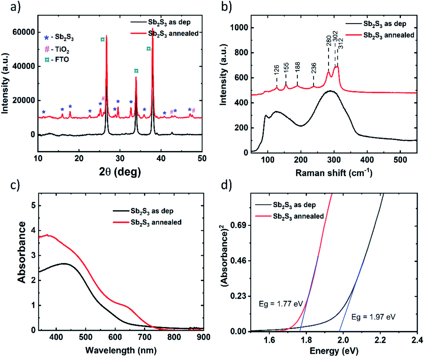 | ||
| Fig. 3 (a) XRD patterns, (b) Raman spectra, (c) absorption spectra and (d) Tauc plots of as-deposited and annealed Sb2S3 films. Substrate: glass/FTO/TiO2. | ||
The images clearly reveal that the surface of the substrates is conformally covered with amorphous Sb2S3 films and the annealed films show a grain structure. Annealing of Sb2S3 films has produced a visual colour change with the as-deposited films turning from orange to dark brown upon annealing (see Fig. S2†). The elemental composition of the as-deposited and annealed Sb2S3 films, determined using energy dispersive X-ray spectroscopy (EDS), shows an atomic ratio of 1.3 for S/Sb. The optical properties of the samples with the as-deposited and annealed Sb2S3 thin films are analysed using UV-Vis-NIR absorption spectroscopy and the corresponding absorbance vs. wavelength curves are shown in Fig. 3c. The spectra reveal that the absorption is stronger in annealed Sb2S3 films with a sharper absorption edge (around 700 nm) compared to amorphous films (around 650 nm). The optical band gap (Eg) of amorphous and crystalline Sb2S3 absorbers is determined using Tauc plots, as shown in Fig. 3d. The allowed band-to-band transitions are considered to be direct in nature while determining the bandgap. The bandgap values of amorphous and crystallized Sb2S3 absorbers are inferred to be 2.1 and 1.8 eV, respectively, which agree well with previously reported values.3,5 The morphological, compositional, structural and optical analyses of annealed Sb2S3 films indicate that the absorber shows conformal coverage on the TiO2 layer, a single stibnite phase and a suitable direct bandgap as desired for solar cell applications. On the crystallized Sb2S3 absorber, V1236 and P3HT are spin coated followed by the thermal evaporation of Au to complete the solar cell fabrication. The detailed synthesis procedure and materials adopted for V1236 are shown in the ESI.† The NMR and mass spectra of intermediate compounds during synthesis and the final V1236 are shown in Fig. S3 and S4,† respectively.
The current density–voltage (J–V) characteristics of the devices are measured under one sun illumination (AM 1.5G) and the J–V curves of the champion cells for each device are shown in Fig. 4 and the corresponding photovoltaic parameters are summarized in Table 1. Primarily, solar cells are prepared using V1236 with a concentration of 15 mM as has been previously used to fabricate perovskite solar cells.29 However, the Sb2S3 solar cells with 15 mM V1236 exhibit a low power conversion efficiency (PCE) of 0.1%, with an open circuit voltage (VOC) of 566 mV, a short-circuit current density (JSC) of 0.87 mA cm−2, and a fill factor (FF) of 0.15. While the reasonable VOC value indicates the formation of the desired p–n junction, the devices hardly have yielded any JSC. The layer thickness of 15 mM V1236 is estimated to be around 140 nm and the resulting series resistance (RS) of the device is estimated to be 17.2 Ω cm2. The extremely low JSC of the solar cell could be attributed to the larger series resistance, which also results in a very low FF. To solve this issue, a series of experiments are carried out where the concentration of V1236 has been systematically reduced (4×, 8×, 16× and 32×). The resulting concentrations of 4 mM, 2 mM, 1 mM and 0.5 mM are used for the HTM layer in the fabrication of solar cells. Fig. 4a shows the J−V characteristics of solar cells with varied V1236 concentrations. As seen from Fig. 4a and Table 1, the concentration dilution has resulted in a considerable increase in PCE particularly arising from significantly higher JSC compared to that of the 15 mM case. The highest PCE of 3.9% is obtained for 2 mM V1236 where the JSC is 13.8 mA cm−2, VOC is 610 mV, and FF is 0.46. However, a further dilution in concentration has decreased the PCE, which is majorly affected by the decrease in VOC. This could be attributed to a plausibly very thin V1236 film owing to the low concentration which may not be enough for the complete coverage of the underlying Sb2S3 absorber. The layer thickness measured in the case of V1236 with 2 mM concentration is found to be ≈20 nm. A positive correlation is found between the concentration of V1236 and its thickness. As the concentration of V1236 decreases from 15 mM to 2 mM, the thickness decreases from approximately 140 nm to 20 nm. A decrease in the concentration of V1236, resulting in thinner films, has also led to a decrease in RS. Furthermore, for a fair evaluation of V1236 as an HTM, optimized solar cells with 2 mM concentration are compared with the devices made using P3HT as an HTM. The concentration of P3HT (0.5, 1 and 2 wt%) has been optimized as shown in Fig. S5,† which shows that solar cells with 1 wt% P3HT have yielded the highest PCE and are therefore used as the reference. The summarized device parameters from JV curves are shown in Table S2.† The J–V curves of solar cells with optimized V1236 and P3HT are compared as shown in Fig. 4b, which indicates almost comparable efficiencies, demonstrating the efficacy of V1236 as an HTM for Sb2S3 solar cells. Furthermore, to understand the impact of HTMs as such, reference devices are made without HTMs, and have yielded a PCE of 2.0% with a lower VOC and FF. This fact affirms the need for HTMs in Sb2S3 solar cells to obtain a higher VOC and hence, efficiency. In addition, to investigate any plausible hysteresis in devices, the forward and reverse J–V characteristics of Sb2S3 solar cells with V1236 and P3HT as HTMs are measured and the plots are shown in Fig. S6.† The J–V curves in forward and reverse directions are almost identical and the calculated hysteresis index (HI) values in both the cases are <0.05 indicating negligible hysteresis in Sb2S3 solar cells with both HTMs.
 | ||
| Fig. 4 J–V curves of the champion Sb2S3 solar cells with (a) different concentrations of V1236 as the HTM. (b) Comparison of cells without an HTM and with optimized V1236 and P3HT. (c) and (d) Cross-sectional images of Sb2S3 solar cells with optimized V1236 and P3HT as HTMs. Structure: glass/FTO/TiO2/Sb2S3/HTM/Au. | ||
| Sample | HTM conc. (mM) | V OC (mV) | J SC (mA cm−2) | FF (%) | PCE (%) | R S (Ω cm2) |
|---|---|---|---|---|---|---|
| Sb2S3/Au | No HTM | 440 | 13.2 | 34 | 2.0 | 4.7 |
| P3HT | 1 wt% | 634 | 11.5 | 50 | 3.7 | 3.1 |
| V1236 | 15 | 566 | 0.9 | 15 | 0.1 | 17.2 |
| V1236 | 4 | 608 | 12.5 | 42 | 3.2 | 0.7 |
| V1236 | 2 | 612 | 13.8 | 46 | 3.9 | 0.6 |
| V1236 | 1 | 614 | 12.5 | 46 | 3.6 | 0.5 |
| V1236 | 0.5 | 552 | 12.2 | 45 | 3.0 | 0.4 |
Cross-sectional images of solar cell stacks with optimized V1236 and P3HT are shown in Fig. 4c and d, respectively. The thickness of TiO2 and Sb2S3 is almost identical in both cases (≈90 nm) while V1236 is a considerably thinner layer (≈20 nm) compared to the P3HT layer (≈100 nm). It is important to note that the V1236 and P3HT are independently optimized for Sb2S3 solar cells leading to higher efficiency, which shows that thinner V1236 is sufficient for obtaining similar efficiencies compared to a reasonably thicker P3HT. Therefore, irrespective of their thickness, the optimized V1236- and P3HT-based solar cells are further characterized and compared for band energetics, quantum efficiency, and overall transparency. The reproducibility of semi-transparent solar cells with V1236 and P3HT HTMs is compared with the box plots as shown in Fig. 5. The spread is not only reasonably small but also almost identical for both the cases and for all the device parameters (VOC, JSC, FF and PCE), indicating the good reproducibility of solar cells.
 | ||
| Fig. 5 Box plots showing reproducibility of (a) VOC, (b) JSC, (c) FF, and (d) efficiency (PCE) for champion Sb2S3 solar cells with V1236 and P3HT as HTMs. Structure: glass/FTO/TiO2/Sb2S3/HTM/Au. | ||
Since V1236 is explored as an HTM for Sb2S3 solar cells for the first time, it is imperative to understand the band edge positions of this material with respect to the absorber for a better understanding of device physics. It is well known that photogenerated electrons in the absorber flow towards the ETL (TiO2) and the holes towards the HTM. The energy levels at the Sb2S3/HTM interface have a strong effect on the hole extraction process. A staggered-gap heterointerface can benefit the process greatly and also prevent the electrons from passing to the HTM layer. The typical curves and the estimation of ionization energy for the V1236 HTM are shown in Fig. S7.†Fig. 6 shows the band energy diagram of solar cells with V1236 and P3HT. The energy levels of FTO, TiO2, Sb2S3, P3HT and V1236 are obtained from photoemission spectroscopy and intrinsic photoconductivity measurements. As clearly revealed in the figure, the HOMO of V1236 (−5.0 eV) is in closer proximity than P3HT (−4.6 eV) to the valence band edge of Sb2S3 (−5.1). This could explain the enhanced performance of V1236 over P3HT due to better hole transport at the absorber–V1236 interface. An interesting observation from Table 1 is that devices with V1236 exhibit a slightly lower VOC than P3HT despite its deeper HOMO level. It may be noted that the observed difference (≈20 mV) in the present study is not significantly large. It is observed that the thickness of V1236 (≈20 nm) is considerably smaller than that of P3HT (≈100 nm) indicating a difference in the interface across Sb2S3/HTM/Au, which may also affect the VOC. In addition, the VOC of the device depends on other parameters like recombination at the absorber–HTM interface, the defects in the absorber, etc., which necessitates deeper analysis like conducting transient photovoltage measurements to analyse the influence of interfacial recombination between the HTM and the absorber layer, which could be investigated further. The LUMO energy level of V1236 (−2.4 eV) is considerably higher than that of P3HT (−2.8 eV) with respect to the conduction band edge (CBE) of Sb2S3 (−3.4 eV). The higher difference between the CBE of Sb2S3 and LUMO of V1236 results in a larger potential barrier (1 eV), which inhibits any chance of electron transport to the Au contact and thus reduces the probability of recombination compared to the P3HT case, which has a smaller energy difference (0.2 eV). The band edge alignment suggests that V1236 could be a potentially more effective HTM than P3HT for Sb2S3 solar cells.
 | ||
| Fig. 6 Energy band diagram of Sb2S3 solar cells with (a) P3HT and (b) V1236 as HTMs. | ||
Furthermore, the external quantum efficiencies (EQEs) of the Sb2S3 solar cells with P3HT and V1236 are studied and the EQE curves are shown in Fig. 7a. EQE curves of solar cells with varied V1236 concentrations are shown in Fig. S8.† While the plots are amply indicative of the fact that the solar cells with V1236 have exhibited a higher spectral response in the entire wavelength range, it may also be noted that the dip in EQE observed for P3HT devices in the 500–700 nm range is absent for V1236 devices. Overall, solar cells with V1236 have exhibited an EQE of ≈ 80% while P3HT devices have yielded 70% in the maximum absorption region, i.e., 400–500 nm. Furthermore, the onset of the absorption edge is situated around 700 nm (1.8 eV), which corresponds to the bandgap of Sb2S3 absorbers, corroborating the optical studies. The integrated JSC values calculated from EQE spectra are shown in Fig. 7a and are calculated to be 13.8 and 11.5 mA cm−2 for V1236 and P3HT, respectively. The values are almost identical to the JSC values obtained from J–V characteristics (Fig. 4b). The impact of polymer-based HTMs on EQE was previously explained by Zimmermann et al.,27 wherein three major mechanisms are held responsible. Primarily, the recombination occurs within the exciton diffusion length of the HTM while a weak electronic bonding or an unfavoured band alignment at the HTM–absorber interface also contributes to enhanced recombination and finally, parasitic absorption in the bulk of the HTM. When light traverses through the absorber, the majority of the light gets absorbed depending on the absorption co-efficient and thickness. If the thickness of the absorber is around 100 nm, some of the light transmits through and gets reflected at the HTM–metal interface, which is supposed to be reabsorbed back in the absorber. However, if the HTM is sufficiently thick (≈100 nm), the reflected light gets absorbed within the HTM, which is responsible for parasitic absorption.27 Thus, optimization of layer thicknesses, and interface modifications are key aspects in Sb2S3–polymer devices. The parasitic absorption coupled with the optical spacer effect of P3HT may be responsible for the overall lower EQE.27 It is also known that P3HT absorbs majorly in the 500–600 nm region due to its bandgap at 1.8 eV,3,5 which further corroborates the dip seen in the EQE curve, thus attributing it to the parasitic absorption.27 Furthermore, the optical spacer effect is dominant when the thickness of the absorber is less than 100 nm, which is the case in the present study. The spectral response in Sb2S3 solar cells is schematically demonstrated in Fig. 7b, which shows the direct absorption of sun light contributing to the carrier generation (indicated as 1), the re-absorption of reflected light from the HTM–metal interface, also contributing to photogeneration (2) and the absorption of reflected light within the HTM layer (3). The spectral response in Sb2S3 solar cells with P3HT may majorly have the phenomena 1 and 3 while V1236 devices may have 1 and 2 owing to the large difference in the thickness of HTMs, which could be witnessed from the EQE curves wherein V1236 devices displayed a larger response compared to P3HT counterparts.
 | ||
| Fig. 7 (a) EQE and integrated JSC of Sb2S3 solar cells with V1236 and P3HT as HTMs and (b) schematic of the spectral response in Sb2S3 solar cells. Structure: glass/FTO/TiO2/Sb2S3/HTM/Au. | ||
To further understand the effect of spectral response, optical properties of individual HTMs coated on glass/FTO substrates are analysed and the total transmittance spectra are shown in Fig. 8a, where the reference curve is also included for the glass/FTO substrate. As can be clearly seen, the transmittance spectrum of glass/FTO/V1236 is almost identical to that of the glass/FTO sample indicating the complete transparency of the V1236 HTM. P3HT, on the other hand, has exhibited a dip in the transmittance around the 500 nm region, which corresponds to the absorption within P3HT (Eg ≈ 1.8 eV). The solar weighted average visible transmittance (AVT) values, calculated in the 400–800 nm region, are compared as shown in the inset of Fig. 8a. The AVT for glass/FTO and glass/FTO/V1236 is almost similar around 80% while that of glass/FTO/P3HT is ≈72%, which further affirms that the optimized V1236 in the present study contributes to more transparency than the P3HT. Furthermore, the total transmittance spectra of V1236 at different concentrations are shown in Fig. S9,† which reveal the transparency of V1236 even for a larger thickness. It may well be noted that the thickness values of P3HT and V1236 compared herein are approximately 100 and 20 nm, respectively, which are optimized for the best efficiency Sb2S3 in each case. Therefore, for a fair comparison of the optical properties, thinner P3HT deposited on glass/FTO, obtained by diluting the concentration, is compared with V1236 as shown in Fig. S10.† Although the thinner P3HT has exhibited enhanced transparency, the relevant absorption edge is still seen, which is majorly responsible for the reduced overall transparency. On a similar note, the total transmittance spectra are recorded for the solar cell devoid of a top metal contact for V1236 and P3HT devices as shown in Fig. 8b. While both the devices have exhibited AVT over 20%, V1236 devices have shown enhanced transparency (about 20% higher) compared to P3HT devices thereby validating the use of V1236 as an HTM in semi-transparent Sb2S3 solar cells.
 | ||
| Fig. 8 Total transmission spectra of (a) glass/FTO, glass/FTO/V1236 and glass/FTO/P3HT layers and (b) Sb2S3 solar cells with V1236 and P3HT as HTMs devoid of a back contact (insets of a and b: respective average visible transmittance bar charts in the 400–800 nm range). | ||
4 Conclusions
In conclusion, a cost-effective and transparent fluorene-based enamine (V1236) hole transport material has been successfully demonstrated, for the first time, in the fabrication of semi-transparent Sb2S3 solar cells yielding a power conversion efficiency of 3.9% with an average visible transmission of 27% in the 400–800 nm spectral range. When compared with conventional P3HT based solar cells, the significantly cheaper V1236 devices have exhibited similar efficiencies and improved transparency. It is observed that the parasitic absorption losses coupled with absorption in the visible range exhibited by P3HT are not present in the case of V1236 thereby validating its efficacy as an HTM for semi-transparent solar cells. Furthermore, the band diagram of solar cells with P3HT and V1236 as HTMs reveals that V1236 is a more effective HTM for the Sb2S3 absorber owing to its improved band alignment. The study, on a whole, put forward the use of new and significantly cheaper V1236 as an HTM in semi-transparent Sb2S3 solar cells, which paves the way towards solar window applications.Author contributions
Nimish Juneja – conceptualization, data curation, formal analysis, methodology, validation, visualization, and writing – original draft. Sreekanth Mandati – conceptualization, investigation, formal analysis, methodology, validation, visualization, supervision, and writing – review & editing. Atanas Katerski – methodology and validation. Nicolae Spalatu – writing – review & editing. Sarune Daskeviciute-Geguziene – methodology and writing – review & editing. Aivars Vembris – methodology and writing – review & editing. Smagul Karazhanov – writing – review & editing. Vytautas Getautis – methodology and writing – review & editing. Malle Krunks – formal analysis, supervision, and writing – review & editing. Ilona Oja Acik – formal analysis, funding acquisition, project administration, resources, supervision, and writing – review & editing.Conflicts of interest
There are no conflicts to declare.Acknowledgements
The “Development of Semi-Transparent Bifacial Thin Film Solar Cells for Innovative Applications” benefits from a 999372 € grant from Iceland, Liechtenstein and Norway through the EEA Grants. The aim of the project is to develop a new approach based on novel materials and structures and production technologies, which are the key to further increase the share, and range of applications of PV in areas with sub-average sunlight, including Baltic and Nordic countries. Therefore, development of resource saving, cost-effective and efficient PV devices is a primary challenge of this project. Project contract with the Research Council of Lithuania (LMTLT) No is S-BMT-21-1(LT08-2-LMT-K-01-003). The Department of Materials and Environmental Technology, Tallinn University of Technology has received funding from Estonian Research Council project PRG627 “Antimony Chalcogenide Thin Films for Next-Generation Semi-Transparent Solar Cells Applicable in Electricity Producing Windows”, the Estonian Centre of Excellence project TK141 (TAR16016EK) “Advanced Materials and High-Technology Devices for Energy Recuperation Systems”, the European Union's Horizon 2020 programme under the ERA Chair project 5GSOLAR grant agreement No 952509 and PSG689 “Bismuth Chalcogenide Thin-Film Disruptive Green Solar Technology for Next Generation Photovoltaics”. Institute of Solid-State Physics, University of Latvia has received funding from the European Union's Horizon 2020 Framework Programme H2020-WIDESPREAD-01-2016-2017-Teaming Phase 2 under grant agreement No. 739508, project CAMART2. The authors thank Dr Tadas Malinauskas and Dr Valdek Mikli for their support in preparation and characterization of the samples.Notes and references
- M. Y. Versavel and J. A. Haber, Thin Solid Films, 2007, 515, 7171–7176 CrossRef CAS.
- S. Messina, M. T. S. Nair and P. K. Nair, Thin Solid Films, 2007, 515, 5777–5782 CrossRef CAS.
- J. S. Eensalu, A. Katerski, E. Kärber, L. Weinhardt, M. Blum, C. Heske, W. Yang, I. Oja Acik and M. Krunks, Beilstein J. Nanotechnol., 2019, 10, 2396–2409 CrossRef CAS PubMed.
- R. Kondrotas, C. Chen and J. Tang, Joule, 2018, 2, 857–878 CrossRef CAS.
- J. S. Eensalu, A. Katerski, E. Kärber, I. Oja Acik, A. Mere and M. Krunks, Beilstein J. Nanotechnol., 2019, 10, 198–210 CrossRef PubMed.
- Y. Itzhaik, O. Niitsoo, M. Page and G. Hodes, J. Phys. Chem. C, 2009, 113, 4254–4256 CrossRef CAS.
- Y. C. Choi, D. U. Lee, J. H. Noh, E. K. Kim and S. il Seok, Adv. Funct. Mater., 2014, 24, 3587–3592 CrossRef CAS.
- Y. C. Choi and S. il Seok, Adv. Funct. Mater., 2015, 25, 2892–2898 CrossRef CAS.
- P. Sun, M. Zhang, C. Ai, Z. Wu, S. Lu, X. Zhang, N. Huang, Y. Sun and X. Sun, J. Power Sources, 2016, 319, 219–226 CrossRef CAS.
- H. Wedemeyer, J. Michels, R. Chmielowski, S. Bourdais, T. Muto, M. Sugiura, G. Dennler and J. Bachmann, Energy Environ. Sci., 2013, 6, 67–71 RSC.
- H.-J. Jo, S. H. Kim, J. S. Kim, S.-J. Lee and D.-H. Kim, J. Korean Phys. Soc., 2016, 69, 541–546 CrossRef.
- R. Parize, A. Katerski, I. Gromyko, L. Rapenne, H. Roussel, E. Kärber, E. Appert, M. Krunks and V. Consonni, J. Phys. Chem. C, 2017, 121, 9672–9680 CrossRef CAS.
- N. Spalatu, R. Krautmann, A. Katerski, E. Karber, R. Josepson, J. Hiie, I. O. Acik and M. Krunks, Sol. Energy Mater. Sol. Cells, 2021, 225, 111045 CrossRef CAS.
- R. Krautmann, N. Spalatu, R. Gunder, D. Abou-Ras, T. Unold, S. Schorr, M. Krunks and I. Oja Acik, Sol. Energy, 2021, 225, 494–500 CrossRef CAS.
- C. P. Liu, H. E. Wang, T. W. Ng, Z. H. Chen, W. F. Zhang, C. Yan, Y. B. Tang, I. Bello, L. Martinu, W. J. Zhang and S. K. Jha, Phys. Status Solidi B, 2012, 249, 627–633 CrossRef CAS.
- N. Ali, A. Hussain, R. Ahmed, W. N. W. Shamsuri, A. Shaari, N. Ahmad and S. M. Abbas, Appl. Phys. A: Solids Surf., 2016, 122, 23 CrossRef.
- M. I. Medina-Montes, Z. Montiel-González, N. R. Mathews and X. Mathew, J. Phys. Chem. Solids, 2017, 111, 182–189 CrossRef CAS.
- Y. Zeng, F. Liu, M. Green and X. Hao, in 2018 IEEE 7th World Conference on Photovoltaic Energy Conversion (WCPEC) (A Joint Conference of 45th IEEE PVSC, 28th PVSEC & 34th EU PVSEC), IEEE, 2018, pp. 0870–0872 Search PubMed.
- L. Guo, B. Zhang, S. Li, Q. Zhang, M. Buettner, L. Li, X. Qian and F. Yan, APL Mater., 2019, 7, 041105 CrossRef.
- W. Lian, C. Jiang, Y. Yin, R. Tang, G. Li, L. Zhang, B. Che and T. Chen, Nat. Commun., 2021, 12, 3260 CrossRef CAS PubMed.
- C. Lan, G. Liang, H. Lan, H. Peng, Z. Su, D. Zhang, H. Sun, J. Luo and P. Fan, Phys. Status Solidi RRL, 2018, 12, 1800025 CrossRef.
- M. S. You, C.-S. Lim, D. H. Kwon, J. H. Heo, S. H. Im and K. J. Chae, Org. Electron., 2015, 21, 155–159 CrossRef CAS.
- D.-H. Kim, S.-J. Lee, M. S. Park, J.-K. Kang, J. H. Heo, S. H. Im and S.-J. Sung, Nanoscale, 2014, 6, 14549–14554 RSC.
- Y. Zhang, S. Li, R. Tang, X. Wang, C. Chen, W. Lian, C. Zhu and T. Chen, Energy Technol., 2018, 6, 2126–2131 CrossRef CAS.
- J. Chen, J. Qi, R. Liu, X. Zhu, Z. Wan, Q. Zhao, S. Tao, C. Dong, G. Y. Ashebir, W. Chen, R. Peng, F. Zhang, S. Yang, X. Tian and M. Wang, Commun. Chem., 2019, 2, 121 CrossRef.
- E. Kärber, A. Katerski, I. Oja Acik, A. Mere, V. Mikli and M. Krunks, Beilstein J. Nanotechnol., 2016, 7, 1662–1673 CrossRef PubMed.
- E. Zimmermann, T. Pfadler, J. Kalb, J. A. Dorman, D. Sommer, G. Hahn, J. Weickert and L. Schmidt-Mende, Adv. Sci., 2015, 2, 1500059 CrossRef PubMed.
- H. Lei, G. Yang, Y. Guo, L. Xiong, P. Qin, X. Dai, X. Zheng, W. Ke, H. Tao, Z. Chen, B. Li and G. Fang, Phys. Chem. Chem. Phys., 2016, 18, 16436–16443 RSC.
- T. Malinauskas, M. Saliba, T. Matsui, M. Daskeviciene, S. Urnikaite, P. Gratia, R. Send, H. Wonneberger, I. Bruder, M. Graetzel, V. Getautis and M. K. Nazeeruddin, Energy Environ. Sci., 2016, 9, 1681–1686 RSC.
- S. H. Im, C.-S. Lim, J. A. Chang, Y. H. Lee, N. Maiti, H.-J. Kim, Md. K. Nazeeruddin, M. Grätzel and S. il Seok, Nano Lett., 2011, 11, 4789–4793 CrossRef CAS PubMed.
- X. Jin, Y. Yuan, C. Jiang, H. Ju, G. Jiang, W. Liu, C. Zhu and T. Chen, Sol. Energy Mater. Sol. Cells, 2018, 185, 542–548 CrossRef CAS.
- L. Zhang, C. Jiang, C. Wu, H. Ju, G. Jiang, W. Liu, C. Zhu and T. Chen, ACS Appl. Mater. Interfaces, 2018, 10, 27098–27105 CrossRef CAS PubMed.
- A. Shit, P. Chal and A. K. Nandi, Phys. Chem. Chem. Phys., 2018, 20, 15890–15900 RSC.
- S. Daskeviciute, C. Momblona, K. Rakstys, A. A. Sutanto, M. Daskeviciene, V. Jankauskas, A. Gruodis, G. Bubniene, V. Getautis and M. K. Nazeeruddin, J. Mater. Chem. A, 2021, 9, 301–309 RSC.
- M. L. Petrus, T. Bein, T. J. Dingemans and P. Docampo, J. Mater. Chem. A, 2015, 3, 12159–12162 RSC.
- F. Machui, M. Hösel, N. Li, G. D. Spyropoulos, T. Ameri, R. R. Søndergaard, M. Jørgensen, A. Scheel, D. Gaiser, K. Kreul, D. Lenssen, M. Legros, N. Lemaitre, M. Vilkman, M. Välimäki, S. Nordman, C. J. Brabec and F. C. Krebs, Energy Environ. Sci., 2014, 7, 2792 RSC.
- J. Latvels, R. Grzibovskis, K. Pudzs, A. Vembris, D. Blumberga, B. P. Rand, C. Adachi, D. Cheyns and V. van Elsbergen, J. Mater. Chem. C, 2014, 91371G Search PubMed.
Footnote |
| † Electronic supplementary information (ESI) available: Synthesis procedure of the V1236 HTM, optical microscopy images of Sb2S3, transmittance and EQE curves. See https://doi.org/10.1039/d2se00356b |
| This journal is © The Royal Society of Chemistry 2022 |