
 Open Access Article
 This Open Access Article is licensed under a
 Creative Commons Attribution 3.0 Unported Licence
Recent developments in perovskite-based precursor inks for scalable architectures of perovskite solar cell technology
Ethan
Berger
a,
Mohammad
Bagheri
 a,
Somayyeh
Asgari
b,
Jin
Zhou
a,
Mikko
Kokkonen
a,
Parisa
Talebi
c,
Jingshan
Luo
d,
Ana Flávia
Nogueira
e,
Trystan
Watson
f and
Syed Ghufran
Hashmi
*a
a,
Somayyeh
Asgari
b,
Jin
Zhou
a,
Mikko
Kokkonen
a,
Parisa
Talebi
c,
Jingshan
Luo
d,
Ana Flávia
Nogueira
e,
Trystan
Watson
f and
Syed Ghufran
Hashmi
*a
aMicroelectronics Research Unit, Faculty of Information Technology & Electrical Engineering, University of Oulu, P. O. Box 4500, FI-90014, Finland. E-mail: ghufran.hashmi@oulu.fi
bOptoelectronics and Measurement Techniques Research Unit, Faculty of Information Technology and Electrical Engineering, University of Oulu, Oulu, Finland
cNano and Molecular Systems Research Unit, University of Oulu, Finland
dInstitute of Photoelectronic Thin Film Devices and Technology, Solar Energy Research Center, Key Laboratory of Photoelectronic Thin Film Devices and Technology of Tianjin, Ministry of Education Engineering Research Center of Thin Film Photoelectronic Technology, Renewable Energy Conversion and Storage Center, Nankai University, Tianjin 300350, China
eLaboratory of Nanotechnology and Solar Energy, Chemistry Institute, University of Campinas – UNICAMP, P. O. Box 6154, 13083-970 Campinas, SP, Brazil
fSPECIFIC, College of Engineering, Baglan Bay Innovation and Knowledge Centre, Swansea University, Baglan SA12 & AX, UK
First published on 4th May 2022
Abstract
The progressive enhancements in solar-to-electrical conversion within the past decade have allowed organic–inorganic lead halide perovskite-based solar cell (PSC) technology to become a competitive candidate for creating affordable and sustainable electricity. This review highlights the developments in fabricating advanced precursor inks of organic–inorganic lead halide perovskite-based light harvesters for large-area perovskite solar cell technology. One of the key characteristics of this promising photovoltaic technology includes solution processing, which offers possibilities to scale up lab-sized solar cell devices into large-area perovskite solar modules comprising unique device architectures. These have been realized in recent years for their deployment in various applications such as building-integrated photovoltaics or internet of things (IoT) devices. In this regard, the presented overview highlights the recent trends that have emerged in the research and development of novel perovskite precursor ink formulations, and it also discusses their contribution toward demonstrating efficient, scalable, and durable PSC technology to create electricity and energize futuristic applications. Various reports were included aiming to showcase the robust photovoltaic performance of large-area perovskite solar modules in a variety of device configurations, hence providing a brief overview of the role of state-of-the-art scalable precursor ink development in transforming unstable lab-sized solar cells into robust, low-cost perovskite solar cell technology that can be scaled up to cover much larger areas.
 Ethan Berger | Ethan Berger received his bachelor's and master's degrees in physical sciences from the Ecole Polytechnique Fédérale de Lausanne (EPFL), Switzerland. For his master's thesis, he worked on the dielectric response of hybrid halide perovskites. He is currently working as a doctoral researcher in computational physics at the Microelectronics Research Unit (MIC) at the University of Oulu, Finland. His current research focuses on Raman spectroscopy from first-principles calculations, molecular dynamics and machine learning. |
 Mohammad Bagheri | Mohammad Bagheri received his master's degree in nanoelectronics engineering from QIAU, Iran. He is currently working as a doctoral researcher in computational materials physics at the Microelectronics Research Unit (MIC) of the Faculty of Information Technology & Electrical Engineering, University of Oulu, Finland. His current research focuses on material modeling and Raman spectroscopy with first-principles calculations, as well as developing high-throughput computations. He is also interested in developing and using materials databases to discover novel materials for energy and quantum technology applications. |
 Somayyeh Asgari | Somayyeh Asgari received her BSc degree in electrical and power electronics engineering from Zanjan University, Zanjan, Iran, in 2014, and her MSc degree in Telecommunications Engineering from K. N. Toosi University of Technology, Tehran, Iran, in 2017. She is doing her PhD research under the supervision of Professor Tapio Fabritius in the Optoelectronics and Measurement Techniques Research Unit, Faculty of Information Technology and Electrical Engineering, University of Oulu, Oulu, Finland. She is an author and co-author of 23 peer-reviewed journals and 3 conference papers. Her research interests include the design and simulation of solar cells, optical metamaterials, chiral metastructures, graphene plasmonic devices and structures, MEMS metamaterials, and linear and nonlinear plasmonic metal-based devices. |
 Jin Zhou | Jin Zhou received his MS degree in Chemical Engineering and Technology from the College of Chemistry, Chemical Engineering and Materials Science, Soochow University, China. Now, he is doing his PhD study in the Microelectronics Research Unit, Faculty of Information Technology and Electrical Engineering, University of Oulu, Finland. His research interests include gas sensors, photoelectric sensors, energy storage devices and perovskites. |
 Mikko Kokkonen | Mikko Kokkonen received his bachelor's and master's degrees in Physics from the University of Oulu, Finland. He is currently a PhD student at the Microelectronics Research Unit of the Faculty of Information Technology & Electrical Engineering, University of Oulu, Finland. His current research focuses on the use of new materials as an RF lens. He is also interested in solar panels and green energy. |
 Parisa Talebi | Parisa Talebi is a PhD student in Physics at the Nano and Molecular Systems Research Unit (NANOMO), University of Oulu, Finland, as a member of the Prof. Wei Cao group. Her research is on ‘noble metal bridged ternary systems for promising clean and sustainable energy’. She obtained her MSc degree in Nano Physics at the University of Arak, Iran, under the supervision of Prof. Maziar Marandi. Her research interests include nanostructures, solar cells, photovoltaics, semiconductors, photocatalysts, hydrogen evolution, synchrotrons, and materials characterization. |
 Jingshan Luo | Jingshan Luo is a full professor and vice director of the Institute of Photoelectronic Thin Film Devices and Technology at Nankai University. He received his BSc degree from Jilin University in 2010 and his PhD degree from Nanyang Technological University in 2014. After that, he went to École Polytechnique Fédérale de Lausanne (EPFL) in Switzerland for postdoctoral research in the laboratory of Prof. Michael Grätzel, where he led the solar fuel subgroup. In 2018, he joined Nankai University. Jingshan Luo has authored/coauthored 1 book chapter and more than 100 peer-reviewed publications in Science, Nature Energy, Nature Catalysis and other journals in the field, which have garnered more than 20 |
 Ana Flávia Nogueira | Prof. Ana Flávia Nogueira obtained her bachelor's degree in Chemistry from the University of São Paulo (1996) and master's (1998) and PhD degrees in Chemistry from the University of Campinas (2001). She worked as a post-doctorate fellow at Imperial College, UK (2001–2002) and as a visiting researcher at Stanford University (2017–2018). At the moment, Ana Flavia is a Full Professor in the Chemistry Institute at UNICAMP and Director of the Center for Innovation on New Energies (CINE, https://www.cine.org.br). Prof. Nogueira's research focuses on the development of functional (nano)materials and their application in solar energy conversion. She has experience in the field of perovskite solar cells, perovskite quantum materials and dense energy carriers (generation of solar fuels through photoelectrocatalytic systems using water, CO2 and other low added value substrates). She has published more than 170 papers, seven book chapters, one book and 3 patents. Her h-index is 40. The Laboratório de Nanotecnologia e Energia Solar (LNES) founded in 2005 has leadership in dye sensitized organic solar cells and perovskite solar research in Brazil and Latin America. In 2020 she was awarded the ACS Leadership in Academia Award. |
 Trystan Watson | Trystan Watson is a Professor in Photovoltaics and Director at the SPECIFIC Innovation and Knowledge Centre. After completing an undergraduate Chemistry Degree and Engineering Doctorate in Steel Technology at Swansea University, Prof. Trystan moved to Corus Strip Products (now Tata Steel) as a product development engineer and a theme leader for the process technology group in the engineering doctorate scheme. In 2007, Prof. Trystan returned to academia to take up a research position in the development of dye-sensitized solar cells on metal substrates. Since then his research has focused on thin film printed PVs with a specialism in developing new technologies for the manufacture of solution processable photovoltaics such as perovskites and OPVs including deposition (roll-to-roll and sheet-to-sheet) and curing processes and their characterisation using electrochemistry, photochemistry and optoelectronic methods. He currently leads PV research at SPECIFIC and his research goal is to take new photovoltaic materials and develop the manufacturing pipeline for fabrication at scale. During his career, Prof. Trystan has published over 150 academic papers and is a chartered engineer with the IOM3 and a fellow of the Royal Society of Chemistry. Trystan is married with three daughters and a son and spends most of his home life wrapped around their fingers. |
 Syed Ghufran Hashmi | Syed Ghufran Hashmi is a Tenure Track Assistant Professor in Printed Electronics at the Microelectronics Research Unit of the University of Oulu, Finland. He has received numerous prestigious funds in the capacity of Project Leader and Principal Investigator from top funding organizations including Technology Industries of Finland Centennial Foundation, Jane and Aatos Erkko Foundation, Business Finland and Academy of Finland for the research and development of next-generation photovoltaic devices such as dye-sensitized solar cells and perovskite solar cells. He received his DSc degree in Engineering Physics from Aalto University – Finland in 2014. Before that, he received his MSc degree in Micro- and Nanotechnology from Helsinki University of Technology – Finland in 2009 and BS degree in Biomedical Engineering from Sir Syed University of Engineering and Technology – Pakistan in 2002. He has authored nearly 30 scientific publications, which have received 1120+ citations. His research interests include solar cells, printed electronics, energy harvesting, solar fuels, printable batteries and supercapacitors. |
1. Introduction
Since its first report,1 the rapid escalation of solar-to-electrical conversion over the last decade (Fig. 1)1–10 has made organic–inorganic lead halide perovskite-based solar cell (PSC) technology a game-changer for creating electricity at an affordable cost.11 Its key features include solution processing, which offers the possibility of rapid production of perovskite solar modules (PSMs), efficient solar-to-electrical energy conversions under various light intensity conditions,12,13 and the well-established long term operational stability under various environmental conditions.12,14–18 Thus, PSC technology has become a unique candidate among other emerging and next-generation-based photovoltaic (PV) technologies19–22 in the emerging area of building-integrated photovoltaics (BIPV)23 and for the next generation of maintenance-free IoT devices.24–26 | ||
| Fig. 1 Solar-to-electrical conversion efficiency evolution of lab-sized perovskite solar cells. | ||
This review highlights the developments being made in the fabrication of advanced scalable precursor inks of organic–inorganic lead halide perovskite-based light harvesters for large-area PSC technology. In the past decade of progressive research, various scalable configurations for PSC technology have been developed.27,28 These have utilized various unique and advanced perovskite precursor inks for achieving efficient large-area PSCs and modules29,30 while demonstrating striking stability when tested under both simulated and natural environmental conditions.16–18 This report summarizes the trends that have emerged during the research and development of producing scalable perovskite precursor ink formulations, and it also discusses their contribution toward efficient, scalable, and durable PSC technology.
To begin with, the various types of scalable device designs are highlighted, along with a brief overview of their inherited advantages and limitations. Various device designs such as n-i-p, p-i-n, and hole transporting material (HTM)-free PSC configurations27,31 are further discussed to establish the general understanding around scaling up approaches being applied on a variety of substrates to produce this low-cost and efficient solar cell technology.
Then, the historical evolution of testing various scalable precursor inks during the development of these configurations starting with lab-sized solar cell devices is presented. Numerous scalable coating schemes used to achieve large-area perovskite-based active layers are also discussed, providing insight into the abundant successes achieved in recent years to produce large-area PSMs. The evolution of state-of-the-art solar-to-electrical efficiencies for various large-area PSMs is also presented.
Various reports highlighting the robust photovoltaic performance of large-area perovskite solar modules in a variety of device configurations are also included in this review, providing a brief overview of the state-of-the-art of scalable precursor ink development in transforming the unstable lab-sized solar cells into large-area, robust, and low-cost solar cell technology. Hence, this review provides the latest insight into the technological research and development in producing novel and scalable precursor inks, as well as their successful integration in various device designs of PSC technology to create electricity and energize futuristic applications.
2. Approaches for scaling-up various device designs of perovskite solar cell technology
The solution processing associated with individual layers of perovskite solar cells (PSCs) greatly influenced the scaling-up of technology from lab-sized devices to large-area modules, which have been fabricated on a variety of substrates.32–38 In this regard, numerous configurations39–42 initially designed to produce lab-sized PSC devices have also been explored to scale-up the technology.43–46 Notably, three fundamental configurations (mesoporous n-i-p, planar n-i-p, and planar p-i-n) have emerged as the most applied in the scaling-up of PSCs (Fig. 2). | ||
| Fig. 2 Three fundamental and scalable configurations: (a) mesoporous n-i-p, (b) planar n-i-p, and (c) planar p-i-n, which have been reported for scaling-up during the emergence of perovskite solar cell technology in recent years (reproduced from ref. 31 with permission from the Royal Society of Chemistry). | ||
Motived by the solid-state dye-sensitized solar cell (ss-DSSC) configuration,22,47,48 perovskite sensitized-based lab-sized solid-state solar cells were initially reported,43,49–51 now known as the mesoporous n-i-p perovskite solar cell device design (Fig. 2a). In this structure, the TiO2-based electron transporting layers (ETLs) are achieved by first fabricating the compact layer (∼5–70 nm in thickness) either by spray pyrolysis,52–56 spin coating44,45,49,57,58 or atomic layer deposition (ALD)59–63 on the desired substrates. After that, an additional mesoscopic layer of TiO2-based ETL is fabricated either by spin coating or screen-printing64–68 processes before depositing the perovskite-based light-absorbing layers, hole transporting layer (HTL), and metal contacts (Table 1).
| Deposition method | Structure | Architecture | Contacts | Precursor ink | Area (active area cm2) | PCE (%) | Substrate | Year | Ref. | ||
|---|---|---|---|---|---|---|---|---|---|---|---|
| Perovskite | ETL | HTL | |||||||||
| Spin-coating | Spin-coating | Spin-coating | Modules p-i-n | p-i-n | LiF/Al | CH3NH3I and PbI2 were stirred in a mixture of DMSO![[thin space (1/6-em)]](https://www.rsc.org/images/entities/char_2009.gif) :GBL (3:7, v/v) :GBL (3:7, v/v) |
10 × 10 (60) | 8.7% @ 1 sun | ITO-glass | 2014 | 95 |
| Spin-coating | Screen-printing | Spin-coating | Modules | Mesoporous n-i-p | Au | CH3NH3I and PbCl2 (molar ratio 3:1) in DMF |
5 × 5 (16.8) | 5.1 @ 1 sun | FTO-glass | 2014 | 96 |
| Spin-coating | Spray pyrolysis | Spin coating | Modules 10 sub-units | p-i-n | Au | MAPbI3 solution (40 wt%) was prepared by mixing the MAI powder and PbI2 (1:1 mole ratio) in DMF |
10 × 10 (40) | 12.9 @ 1 sun | FTO-glass | 2015 | 97 |
| Slot-die coating | Slot-die coating | Slot-die coating | Modules | n-i-p | Ag | PbI2 (322 mg mL−1 in DMF) and CH3NH3I (10 mg mL−1 in 2-propanol) | 10 × 10 (40) | 11.96 @ 1 sun | ITO-glass | 2015 | 98 |
| Dropping by micropipette | Screen-printing | — | Modules | n-i-p | C | The equimolar ratio of PbI2 and CH3HN3I in γ-butyrolactone | 10 × 10 (70) | 10.74 @ 100 W white light LED light | FTO-glass | 2016 | 99 |
| Spray coating | Spray pyrolysis | Spin coating | Modules | n-i-p | Au | Mixed solution of DMF (dimethylformamide):γ-butyrolactone (GBL) (v/v) to prepare the 0.8 M MAPbI3−xClx |
10 × 10 (40) | 15.5 @ 1 sun | FTO-glass | 2016 | 100 |
| Dipping PbI2 substrates into MAI in IPA solution | Spray pyrolysis/spin coating | Air assisted blade-coating | Modules | Mesoporous n-i-p | Au | PbI2 substrates and MAI in IPA solution (10 mg mL−1) | 10 × 10 (50) | 12.6 @ 1 sun | FTO-glass | 2017 | 101 |
| Pressure processing | Spin coating | Spin coating | Single-cell | Mesoporous n-i-p | Au | CH3NH3I·3CH3NH2 and PbI2·CH3NH2, in a molar ratio of 1:1; CH3NH3I·3CH3NH2 and PbI2·CH3NH2 precursors were prepared by inducing CH3NH2 gas |
8 × 8 (36.1) | 12.1 @ 1 sun | FTO-glass | 2017 | 102 |
| Vapor–solid reaction method | Soaking and heating | Spin coating | Modules | n-i-p | Au | CsxFA1−xPbI3−yBry | 8 × 8 (41) | 12.24 @ 1 sun | FTO-glass | 2018 | 50 |
| Megasonic spray-coating | Thermal evaporation | Spin-coating | Single-cell | p-i-n | Cu | 400 mg mL−1 PbI2 in DMF/DMSO (volume ratio = 1:1) and MAI powder |
7.5 × 7.5 (18) | 16.9 @ 1 sun | ITO-glass | 2018 | 57 |
| Inkjet printing | Spin coating | Spin-coating | Single-cell | Mesoporous n-i-p | Au | CH3NH3PbI3 | ∼3.1 × 3.1 (2.02) | 17.74 @ 1 sun | FTO coated substrate | 2018 | 39 |
| Spin coating | Spin coating | Spin coating | Single-cell | n-i-p | Ag | [CsPbI3]0.05[(FAPbI3)0.85(MAPbBr3)0.15]0.95 in DMSO/DMF with a 5% molar ratio PbI2 excess | 14 × 14 (1.08/2 × 2 cell) | 17.39 @ 1 sun | FTO-glass | 2018 | 45 |
| Bar-coating | Bar-coating | Spin coating | Modules | n-i-p | Au | MAI and PbI2 at an equimolar ratio were dissolved in mixed NMP:DMF (9:2) |
8 × 10 | 17.28 @ 1 sun | ITO-glass | 2019 | 103 |
| Blade-coating | Spin coating | Spin coating | Single-cell | n-i-p | Au | 461 mg of PbI2, 78 mg of DMSO, and 159 mg of MAI dissolved in 600 mg of DMF and 0.05% ZnP | 4 × 4 | 20.5 @ 1 sun | FTO-glass | 2019 | 44 |
| Air-knife-assisted D-bar coating | Spin coating | Spin coating | Single-cell | n-i-p | Au | 0.12 mmol GAI, 1.78 mmol MAI, 0.7 mmol PbI2 (10 mol% PbI2 excess) and 0.4 mmol PbAc2 were dissolved in 1 mL 2-ME | 4.8 × 9.6 (16) | 13.85 @ 1 sun | FTO-glass | 2019 | 104 |
| Solution-bathing | Spin coating | Spin coating | Single-cell | p-i-n | Au | PbI2 (1.15 M), FAI (1.09 M), PbBr2 (0.20 M), MABr (0.14 M) and CsI (0.06 M) in a mixed solvent of DMF/DMSO/NMP (DMF/DMSO, 4/1, v/v) | 5 × 5 (1.00) | 18 @ 1 sun | ITO-glass | 2020 | 58 |
| D-bar coating | Spin coating | Spin coating | Modules 10 sub-cells | n-i-p | Au | Dissolving 553.8 mg of the FAPbI3 powder, 26.6 mg of CsBr, 45.8 mg of PbBr2, and 20.4 mg of MACl in 700 μL DMF or HMPA; for the Lewis base additive, 0.6 mmol DMSO or 0.6 mmol HMPA was included in the precursor solution | 5 × 5 (18.66) | 17.01 @ 1 sun | FTO-glass | 2020 | 43 |
| Spin-assisted solvent extraction | Spin coating | Spin coating | Modules | n-i-p | Ag | An equal amount of MAI and PbI2 (or FAI, MAI, and PbI2 mixture or FAI, MAI, PbI2, and PbBr2 mixture) was dissolved in 2P to make a precursor solution with a concentration of 1.5 M | 10 × 10 (25.2) | 14.36 @ 1 sun | ITO-glass | 2020 | 105 |
| Slot-die coating | Slot-die coating | Slot-die coating | Single-cell/modules | p-i-n | Ag | 276 mg PbI2, 96 mg MAI, and 0.18 mg PEG were dissolved in the solvent mixtures of GBL and DMSO | 2 × 2 (0.09; cut from 12 × 12)/4 × 4(3.78) | 11 @ 1 sun/10.34 @ 1 sun | FTO-glass | 2020 | 106 |
| HPNE strategy assisted slot-die coating | Chemical bath deposition | Spin coating | Modules | n-i-p | Au | FA0.91Cs0.09PbI3 perovskite precursor was prepared in a mixed solvent (DMF:DMSO = 4.75:1) with a concentration of 1.25 M, 23 mol% MACl was added |
0.6 × 3.4 × 5-sub-cell (10.2) | 18.6 @ 1 sun | FTO-glass | 2020 | 41 |
| Slot-die method | Slot-die method | Slot-die method | Modules | n-i-p | Cr/Au | 553.2 mg PbI2 and 15.6 mg CsI were dissolved in 0.9 mL DMF and 0.1 mL DMSO; 75 mg FAI and 2.5 mg FACl were dissolved in 1 mL isopropanol | 8 × 8 (35.80) | 15.3% @ 1 sun | FTO-glass | 2021 | 107 |
| Spin-coating | Spin-coating | Spin-coating | Modules | n-i-p | Au | 2.2 M PbI2 and 28 mg CsI were dissolved in 1 mL DMF solution with different molar ratios of NH4Cl (0, 0.1, 0.2, 0.3, 0.4, 0.5, 0.7 and 1.0 M) | 10 × 10 (91.8) | 10.25% @ 1 sun | ITO-glass | 2021 | 108 |
| Spin-coating | Chemical bath deposition | Thermal evaporation method | Modules | n-i-p | Au | 1.35 M PbI2 and 0.0675 M CsI were dissolved in a mixed solution (1.9 mL DMF and 0.1 mL DMSO); FAI 1000 mg; MAI 110 g; MABr 110 mg; MACl 110 mg, dissolved in 15 mL IPA | 10 × 10 (91.8) | 21.70% @ 1 sun | FTO-glass | 2021 | 109 |
| Spin-coating | Spin-coating | Spin-coating | Modules | n-i-p | Au | Lead iodide (1.51 M), formamidinium iodide (1.47 M), methylammonium bromide (0.03 M), lead bromide (0.03 M), and methylammonium chloride (0.6 M) in the mixed solvent of DMF:DMSO (8/1; v/v) |
10 × 10 (45.6) | 17.97% @ 1 sun | FTO-glass | 2022 | 110 |
Nevertheless, the mesoporous TiO2 has been systematically removed from the mesoporous n-i-p device design, for the following reasons: (1) achieving low temperature and binder-free based ink or paste formulations of nanoparticles based on TiO2 has remained challenging when attempting to achieve scalable mesoporous n-i-p-based configurations on flexible polymer substrates. (2) The additional step of fabricating a mesoporous TiO2-based ETL in the device structure induces additional cost and time, which may limit the competitiveness of the technology compared to other existing solutions.
As a result, the n-i-p-based planar structure (Fig. 2b) gained attention since it can achieve good solar-to-electrical conversion efficiencies upon removing the mesoporous ETL layers from the traditional n-i-p device design of PSCs. Moreover, inspired by the solution processing of organic solar cells,69–73 scaling-up schemes of PSC technology with a planar n-i-p device design have also been rapidly developed and demonstrated both on flexible polymers and rigid glass-based substrates.32,41,45,46,74,75
Similarly, the inverted structure of the p-i-n device design (Fig. 2c) has also been realized recently because of the availability of a wide range of material-based ink formulations already tested in lab-sized devices as well as in large-area module configurations, with impressive solar-to-electrical conversion efficiencies (Table 1).
In contrast to these traditional configurations, other scalable device designs i.e., HTM- and metal contact-free carbon-based perovskite solar cell configurations (Fig. 3) have also been reported in recent years.76–85 These novel device designs have emerged by first replacing the ruthenium dyes and liquid electrolytes from the monolithic DSSC configurations with a perovskite sensitizer.86–88 This strategy allowed a low-cost, printable, and solid-state device configuration that demonstrated impressive solar-to-electrical energy conversion combined with exceptional stability when exposed to numerous simulated and natural climatic conditions.1,89–92Table 1 provides an overview of the scalable perovskite solar cells produced in various device designs. Fig. 4 represents the actual demonstrations of perovskite solar modules produced in some of the most established configurations discussed earlier in this section.
 | ||
| Fig. 3 Scalable carbon-based configurations. (a) Carbon-based perovskite solar cell (C-PSC) configuration (reproduced from ref. 93 with permission from the Royal Society of Chemistry). (b) C-PSC with a ZrO2 spacer to keep the carbon layer separated from the photoanode (reproduced from ref. 94 with permission from the Royal Society of Chemistry). | ||
 | ||
| Fig. 4 Examples of various types of large-area perovskite solar modules fabricated on rigid and flexible substrates. (a) A mesoporous glass-based n-i-p solar module (reproduced from ref. 30 with permission from Elsevier, copyright 2022). (b) A planar n-i-p glass-based perovskite solar module (reproduced from ref. 111 with permission from the Royal Society of Chemistry). (c) An inverted p-i-n configured glass-based perovskite solar module (reproduced from ref. 95 with permission from the Royal Society of Chemistry). (d) An inverted p-i-n-based flexible solar module fabricated on PET polymer substrates (reproduced from ref. 112 with permission from the American Chemical Society). (e) A carbon-based triple-mesoscopic printable perovskite solar module on a rigid glass substrate (reproduced from ref. 66 with permission from Elsevier, copyright 2022). | ||
3. Historical evolution of perovskite precursors tested for scalable perovskite solar cells and modules
The solution processing associated with active layers of PSC technology, including perovskite-based light-absorbing layers, has greatly motivated research groups worldwide to create their novel and scalable precursor solutions that could be integrated into scalable cell architectures via various scalable material deposition methods, such as blade coating, inkjet printing, slot-die coating, or spraying-based material deposition technologies.One of the initial studies was reported by Matteocci and co-workers, who demonstrated the first scalable and fully solid-state n-i-p-based perovskite solar modules (PSMs) fabricated on rigid glass substrates.96 Interestingly, the spin-coating technique was chosen for the perovskite precursor ink deposition, comprising a mixed halide solution in N,N-dimethylformamide (DMF) (Table 2) for the development of their 5 × 5 cm2 PSM. The fabricated modules containing two types of HTMs exhibited similar (5.1%) solar-to-electrical energy conversion when tested under full sunlight illumination. Nevertheless, the modules fabricated with the traditional HTM (i.e., Spiro-OMeTAD) exhibited higher long-term stability by maintaining more than 60% of their initial efficiency after 335 hours, compared to the alternative poly(3-hexylthiophene-2,5-diyl) (P3HT) polymer-based PSMs, in which the conversion efficiency was reduced by about 80% of the initial value after 170 hours.
| Device structure | Perovskite precursor ink | Active area (cm2) | PCE (%) | Year | Ref. |
|---|---|---|---|---|---|
| a Aperture area. | |||||
| Glass/FTO/c-TiO2/n-TiO2/perovskite/P3HT/Au | Methylammonium iodide CH3NH3I and lead chloride PbCl2 in N,N-dimethylformamide, molar ratio 3:1 |
16.8 | 5.1 | 2014 | 96 |
| Glass/ITO/PEDOT:PSS/perovskite/PCBM/LiF/Al |
The CH3NH3I and PbI2 were stirred in a mixture of DMSO:γ-butyrolactone (GBL) (3:7, v/v) at 60 °C for 12 h |
60 | 8.7 | 2014 | 95 |
| Glass/FTO/BL-TiO2/perovskite/Spiro-OMeTAD/Au | The 0.6 mL per sample of CH3NH3PbI3−xClx perovskite precursor solution (40 wt%) was deposited by spin-coating at 2000 rpm for 60 s | 10.08 | 13 | 2016 | 114 |
| Glass/FTO/c-TiO2/perovskite/Spiro-OMeTAD/Au | The typical recipe for 45 wt% precursor with 30% MACl additive is 0.2 g MAI, 0.580 g PbI2, 0.025 g MACl, 0.524 g NMP and 0.429 g DMF | 11.09 | 14.06 | 2017 | 115 |
| PET/ITO/SnO2/Cs0.05(FA0.85MA0.15)0.95Pb(I0.85Br0.15)3/Spiro-OMeTAD-Au | Dissolving 1.3 M organic cations (0.85 FAI and 0.15 MABr) and a 1.4 M mixture of metal lead salts (0.85 PbI2 and 0.15 PbBr2) in a solvent of DMF/DMSO (4:1, by volume), and then a 34 μL CsI solution (pre-dissolved as a 2 M stock solution in DMSO) added |
16.07 | 14.89 | 2018 | 116 |
| Glass/FTO/c-TiO2/mp-TiO2/MAPbI3−xClx/Spiro-OMeTAD/Au | Different molar ratios of MACl/HPbI3 are deposited on substrates. After thermal annealing, the obtained films react with CH3NH2 gas to form perovskite | 12 | 15.3 | 2018 | 117 |
| Glass/FTO/NiO/perovskite/DBL/G-PCBM/Ag | 424 mg FAI, 1.136 mg PbI2, 49 mg CH3NH3Br, and 160 mg PbBr2 dissolved in 2.4 mL acetonitrile | 36.1a | 15.6 | 2019 | 118 |
| PEN/ITO/np-SnO2/porous-ZSO ETL/(FAPbI3)0.95(MAPbBr3)0.05/Spiro-OMeTAD/Au | 1.26 mmol of PbI2, 1.26 mmol of FAI, 0.06 mmol of MAPbBr3, and 0.5 mmol of MACl in DMF/DMSO | 90 | 15.5 | 2020 | 119 |
| MgF2/Willow glass/ITO/PTAA/MAPI-NH4Cl/C60/BCP/Cu | L-α-Phosphatidylcholine and methylammonium hypophosphite were added into ≈1.45 M MAPbI3/2-ME solution at a concentration of ≈0.3 mg mL−1 and ≈0.15 vol%. 6 × 10⁻³ M NH4Cl was added to the precursor | 42.9 | 15.86 | 2020 | 120 |
| Glass/FTO/ZnO–ZnS/mp-TiO2/CH3NH3PbI3/Spiro-OMeTAD/Au | 1 mmol of MAI, 1 mmol of PbI2, and MACl (<20 mol% of MAPbI3) were dissolved in an 800 μL solution of CH3NH2 solution in ethanol, and 200 μL of CAN | 12a | 16 | 2020 | 121 |
| PEN/hc-PEDOT:PSS/NiOx/perovskite/PCBM/Ag |
547 mg PbI2, 46 mg PbBr2, 150 mg FAI, 39 mg MAI and 0.02 wt% PU in 1.5 mL anhydrous DMF and 1.5 mL anhydrous DMSO | 15 | 16.15 | 2021 | 113 |
| Glass/FTO/c-TiO2/mp-TiO2/Perovskite/MW doped-PTAA/Au | FAPbI3 (1.47 M) and MAPbBr3 (0.18 M) precursor complexes in 1 mL of mixed DMF/DMSO solvent and 0.05 M CsI | 42.8 | 17.05 | 2021 | 122 |
| Glass/FTO/TiO2/perovskite/[M4N]BF4/Spiro-OMeTAD/Ag | The FA0.91Cs0.09PbI3 perovskite precursor was prepared in a mixed solvent (DMF:DMSO = 4.75:1) with a concentration of 1.25 M, 23 mol% MACl was added |
7.92 | 19.0 | 2020 | 123 |
| Glass/FTO/TIO2/SnO2/ink/BJ-GO/Spiro-OMeTAD/Cr/Au | 645.4 mg PbI2 and 18.2 mg CsI were dissolved in 0.9 mL DMF and 0.1 mL DMSO for the first deposited solution. 90 mg FAI and 4 mg FACl were dissolved in 1 mL isopropanol for the second solution | 35.8 | 15.3 | 2021 | 107 |
This preliminary demonstration motivated research labs worldwide to further develop novel precursors that could be integrated into the desired scalable device configurations of PSC technology through established large-scale material deposition methods. For example, Xu and co-workers demonstrated a novel perovskite precursor ink that was introduced in triple mesoscopic carbon-based printable solar modules.66 The novel precursor ink used in their study contained 5-ammonium valeric acid (5-AVAI) as a perovskite crystallization retarding agent, in addition to methylammonium iodide (MAI) and PbI2, which were dissolved in γ-butyrolactone (GBL) solvent to attain the stable and compatible perovskite precursor ink formulation. As a result, successful fabrication of carbon-based PSMs was achieved by incorporating this novel precursor formulation through the slot-die coating technique over an aperture area of 80.55 cm2. This resulted in achieving a striking conversion efficiency (12.87%) with an active area of 60.08 cm2 when recorded under full sunlight illumination.
Contrary to the precursor inks demonstrated in the fabrication of rigid glass-based PSMs, other novel precursor inks have also been developed to produce large-area flexible perovskite solar cells and modules.98,113 For example, Wang et al. recently reported a one-step perovskite precursor ink solution by dissolving PbI2, PbBr2, formamidinium iodide (FAI), MAI, and 0.02 wt% PU in 1.5 mL anhydrous DMF and 1.5 mL anhydrous dimethyl sulfoxide (DMSO) mixture solvent.113 This novel precursor ink was meniscus-coated on the pre-HTL coated ITO-PET substrate to fabricate a large-area flexible solar module that exhibited impressive (>16%) solar-to-electrical energy conversion when tested under full sunlight illumination.
On the other hand, Castriotta and co-workers developed a blade-coated scalable precursor ink of the perovskite light-absorbing layer to produce a flexible perovskite solar module on an ITO-PET substrate.112 A Cs0.17FA0.83Pb(I0.9Br0.1)3-based precursor ink was produced by dissolving CsI, PbBr2, FAI, and PbI2 in 1 mL of N-methyl-2-pyrrolidone (NMP)/DMF solvent, which was deposited on the HTL-coated ITO-PET substrate with N2-assisted blade-coating, followed by heating (100 °C) for 45 minutes. With this inverted device design produced on an ITO-PET substrate, the flexible module also exhibited >10% power conversion efficiency (PCE) over a 15.7 cm2 active area by exploiting blade deposition of the transporting layer and a stable double-cation perovskite (cesium and formamidinium, CsFA)-based light-absorbing layer. More impressively, outstanding light stability of the fabricated modules – over 1000 h, considering the recovery time (T80 = 730 h) – was also demonstrated, thus reinforcing the potential of this low-cost solution-based PV technology. Table 2 highlights some of the high-performing large-area modules that are being developed by incorporating scalable precursor inks of the perovskite-based light-absorbing layer.
4. Rheological characteristics of perovskite precursor inks and scalable coating methods for deposition of large-area perovskite precursors
Interestingly, the progressive transition not only induced innovativeness in scalable device designs, but also provided opportunities to develop advanced perovskite precursor inks via examining their rheological characteristics to facilitate the upscaling goals of PSC technology.In this regard, various reports have frequently surfaced that highlight key rheological parameters (Fig. 5) such as contact angles, viscosity, density, surface tension, or boiling points of the fabricated perovskite precursor inks.15,29,124–131 Such interesting trends led to the demonstration of various scalable device architectures of PSC technology fabricated by employing scalable perovskite-based precursor ink formulations along with scalable coating methods.
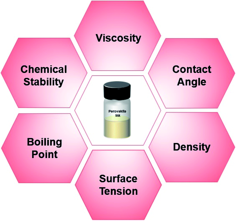 | ||
| Fig. 5 Key rheological characteristics of high-performance perovskite precursor inks. | ||
For example, Huang et al. reported the formulation of a novel PbI2 ink by mixing traces of MAI and polyurethane (PU) as an additive with PbI2 in the DMF/DMSO solvent mixture.129 This novel ink engineering strategy regulated one of the key factors of rheological properties (i.e., the viscosity) and influenced the chemical stability of the fabricated PbI2 ink. As a result, both the successful room temperature-based scalable deposition of PbI2 layers and the complete scalable deposition of perovskite light absorbing layers under ambient conditions were demonstrated through the two-step processing approach. An impressive 11.07% solar-to-electrical conversion efficiency was achieved for a 25 cm2 based large-area perovskite solar module (PSM) when configured in a p-i-n based inverted configuration.
In contrast, single-step processable inks have also been reported by incorporating starch as a ‘rheological modifier’,126,127 which created a suitable viscosity for the fabricated perovskite inks to be deposited with a suitable thickness without increasing the concentration of perovskite precursors.126 Roll-to-roll perovskite-based printed films and flexible solar cells have recently been demonstrated utilizing such inks, reaching a maximum power conversion efficiency close to 10% with required viscosities, with 50% less usage of the raw precursor materials along with a single processing step.126
Combined with advancements in similar rheological characteristics research, the rapid technological developments for material deposition schemes have also made it possible to achieve scalable layer formations of active layers for various next generation-based solar cell technologies.132–134 This not only enables scalability of the energy systems but also achieves electrical, optical, dielectric, or optoelectronic properties of active layers with a reliable process control.135–137
In this regard, various scalable coating methods for large-area perovskite precursor deposition similar to other next generation-based PV technologies have also been explored to develop large area-based PSC technology on numerous substrates.138–140 Some of these established scalable coating methods have been discussed in the following sub-sections.
4.1 Slot-die coating of perovskite precursor inks
Slot-die coating has remained one of the most popular schemes in fabricating flexible organic solar cells, as it allows the possibility for rapid coating and roll-to-roll fabrication of active layers on flexible substrates.141–143 In this process, the slot-die head is placed close to the substrate and the ink is pumped into the head using a syringe. This creates a bridge of ink between the head and the substrate, which allows for a clean and rapid deposition of active layers on the desired substrates (Fig. 6).141,144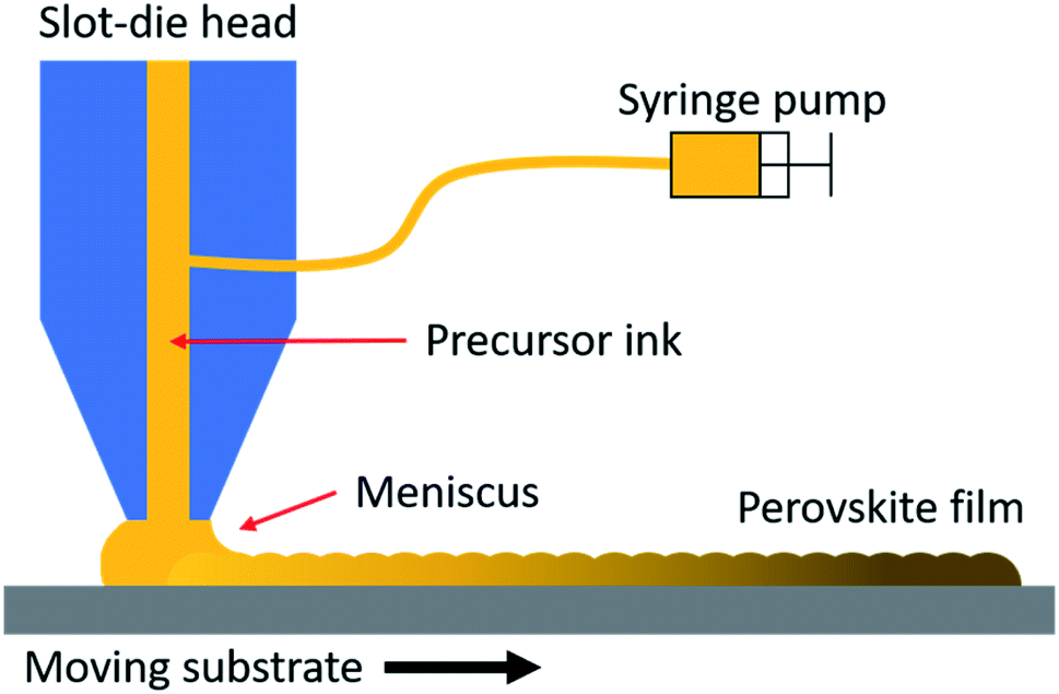 | ||
| Fig. 6 Schematic illustration of the slot-die coating process. | ||
Vak et al. reported one of the first demonstrations of slot-die coating for producing a perovskite light-absorbing layer by modifying a 3D printer with a two-step processing approach.145 First, the precursor ink of PbI2 was coated on ZnO and dried to produce a PbI2-coated ETL layer. Next, the substrate containing the active layers was dipped in the MAI solution to obtain the perovskite layer. Finally, the PSC assembly was completed by fabricating a P3HT-based hole transporting layer (HTL) and vacuum evaporating the silver (Ag) contact layer. The fabricated PSC exhibited an efficiency of 11.6%.
As a further advancement, large-area and roll-to-roll fabrication of glass and flexible perovskite solar cells, respectively, in a planar n-i-p configuration was demonstrated with slot-die printed active layers, except for the evaporated metal electrode.98 In this work, the perovskite light-absorbing layer was also achieved with a two-step material deposition process, where the PbI2 ink in DMF solvent was first slot-die coated on a ZnO-based ETL layer with various optimizations using gas quenching treatments. Next, the MAI solution was also coated with the same slot-die coating process to crystallize the perovskite light-absorbing layer. The HTL was achieved by coating with a P3HT solution followed by vacuum evaporation of the Ag contact layer. The fabricated devices on glass showed an efficiency of 11.96% on glass substrates. In contrast to rigid substrates, flexible perovskite solar cell modules were produced with roll-to-roll production on a 10 cm × 10 cm polymer substrate with five serially connected cells.
Demonstrations of single-step slot-die coatings are also reported wherein mixed cations,146,147 additives,148,149 and compatible solvents have been used to achieve homogeneous and large-area perovskite light-absorbing layers.66,141 For example, Schmidt et al. reported a single-step slot-die processable coating of perovskite precursor ink that achieved 4.9% conversion efficiency on flexible ITO-PET substrates.138 Slot-die coating of a novel precursor ink for triple mesoscopic printable perovskite solar modules was also recently demonstrated; a conversion efficiency of ∼13% was obtained over an active area of 60.08 cm2 when measured under full sunlight illumination intensity.66
These demonstrations suggest that single-step coating processes with slot-die coating might be more suitable for large-scale production of PSC technology. Reaching the desired result is made possible by forming a favorable combination of suitable precursor ink and substrate, along with the improved drying process of the precursor ink and its associated crystal growth.
4.2 Inkjet printing of perovskite precursor inks
The inkjet printing technique offers precise drop on demand (DOD)-based patterning for a variety of materials. In this method, the precursor ink remains stored in a nozzle, and pressure is created through a piezoelectric device to form the droplets. This allows for very precise control over the ink flow, which results in the smooth deposition of active materials over several types of substrates (Fig. 7).150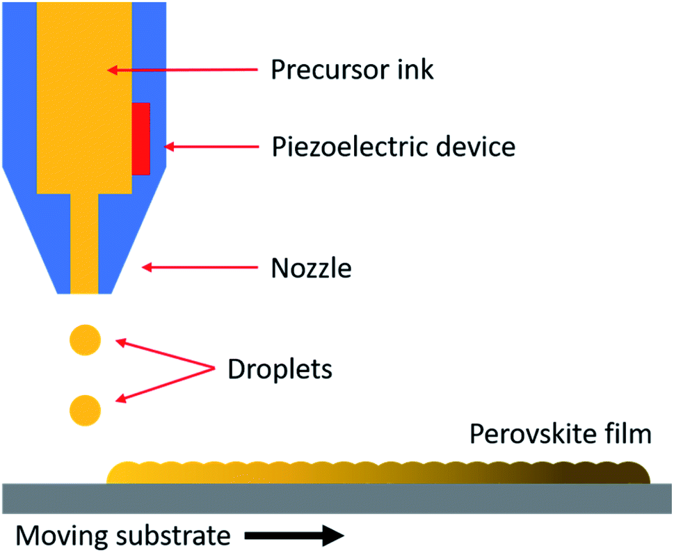 | ||
| Fig. 7 Schematic illustration of the inkjet printing process. | ||
The scalability from lab-sized devices to large-area modules can be achieved by the rapid inkjet printing process, where individual layers like in slot-die coating can be printed directly on the desired substrates. Hashmi et al. demonstrated inkjet infiltration of a perovskite precursor ink on lab-sized PSCs and highlighted the performance reproducibility and reliable process control among the fabricated individual cells of the triple mesoscopic printable perovskite solar cells.15 Similarly, Li et al. demonstrated inkjet printing of the perovskite precursor in the mesoporous n-i-p device configuration, where the perovskite precursor ink was deposited on TiO2-based ETLs. The devices showed an efficiency of 12.3% in lab-sized PSC devices when measured under full sunlight intensity.151
Recently, Panasonic Corporation announced 16.09% solar-to-electrical energy conversion for a glass-based large-area perovskite solar module by using a coating method based on inkjet printing. In their module, every individual layer of the device design – including the perovskite layer – was deposited utilizing inkjet printing technology.152 Another commercial player has also been developing large-area inkjet-printed flexible perovskite solar modules, which have started to become integrated into their commercial products.153
4.3 Blade-coating
Blade-coating is another potentially scalable deposition method that is widely used in various demonstrations of fabricating perovskite solar cells.154–157Fig. 8 illustrates the schematic of the blade-coating process, in which the precursor ink is dropped in front of a metallic or glass blade and then swept forward on a moving substrate to deposit a wet precursor layer.158,159 The perovskite film thickness is determined by a few factors, including the meniscus of the solution that forms between the blade and substrate, the speed of the moving blade, the viscosity of the ink, and the concentration of the precursor ink. | ||
| Fig. 8 Schematic illustration of the blade-coating process. | ||
Similar to slot-die coating, both single- and two-step processing approaches can be applied to perovskite light-absorbing layer fabrication.154,156 Gas and solvent quenching, and heating techniques have also remained popular schemes for controlling the crystallization and drying of the wet layers deposited through blade-coating from their respective precursor inks.160,161
Deng et al. performed single-step blade-coating of a perovskite precursor ink on glass substrates, by which 12.8% and 15.1% solar-to-electrical conversion efficiencies were achieved with two different HTM layers.139 The fabricated ink was obtained by dissolving MAI and PbI2 (1:1 molar ratio) in DMF, which was then coated with a glass blade on two different HTM (PEDOT:PSS and c-OTPD:TPACA) layers to fabricate and compare the inverted p-i-n configuration. A large grain-sized crystal-based perovskite layer was achieved with the demonstrated blade-coating method, which was effective over a long carrier diffusion length and led to high conversion efficiencies when tested under simulated full sunlight illumination.
In another study, Tang et al. applied a novel approach of mixing cesium (Cs+) and bromine (Br−) ions into the perovskite precursor solution, which also reduced the required film formation temperature.135 Pinhole-free perovskite thin films with micrometer-sized grains have been obtained with the assistance of secondary grain growth with methylammonium chloride added into the precursor solution. The fabricated PSCs using such bladed perovskite layer attained an impressive 19.0% solar-to-electrical energy conversion; the best-stabilized conversion efficiency reached 19.3%.135 Zhang et al. reported an impressive demonstration of an n-i-p design with two-step sequential blade-coating of high-quality perovskite layers for producing efficient solar cells and modules.162 Their fabrication scheme involved the production of a SnO2-based compact layer, achieved with a chemical bath process. Next, the sequential blade-coating steps were performed: DMF containing PbI2-based precursor ink was first bladed over the compact layer and heated to achieve PbI2 films. Then the mixed solution of FAI, methylammonium bromide (MABr), and methylammonium chloride (MACl) in isopropanol (IPA) was sequentially bladed over the PbI2 layers, followed by an annealing step at 150 °C for perovskite crystallization. The fabricated solar cells with this two-step blade-coated processing yielded a conversion efficiency as high as >20% among lab-sized solar cells, whereas the large-area (5 cm × 5 cm and 10 cm × 10 cm) modules exhibited 16.54% and 13.32% conversion efficiencies, respectively.
4.4 Spraying
Similar to the previously discussed scalable fabrication schemes, spraying has also been widely used for precursor ink deposition to achieve large-area perovskite layers but also, deposition of other transporting layers.100,163 This solution-based deposition scheme typically utilizes an ultrasonic tip vibrator to create a solvent mist or ink droplets that are directed to the substrate.163 To do this, N2 or O2 can be used as a carrier gas to produce wet films on the desired substrates (Fig. 9).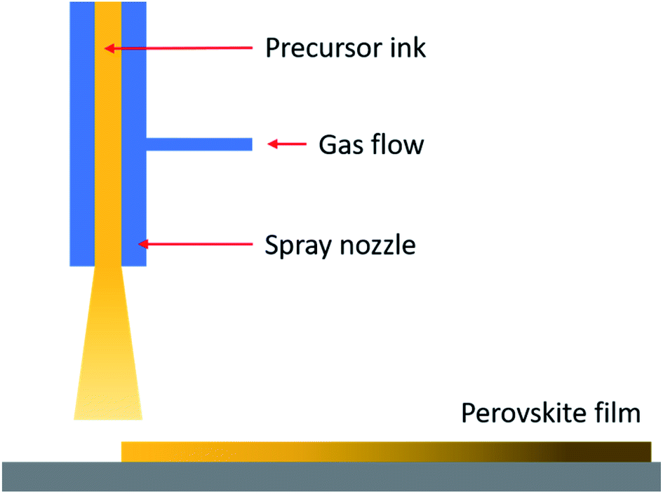 | ||
| Fig. 9 Schematic illustration of the spraying process. | ||
Barrows et al. coated perovskite layers with a single step by spraying mixed solutions of MAI and PbCl2 in DMF and DMSO solvents over PEDOT:PSS, and achieved 11% solar-to-electrical conversion efficiency in the inverted p-i-n configuration for lab-sized PSCs.164
Boopathi et al. controlled the volume of MAI through airbrush spraying followed by the deposition of PbI2 through spin-coating to attain a uniform, stoichiometric and continuous perovskite film.165 Their experiments showed that either a deficiency or surplus in the volume of MAI generates poor crystallinity and morphology, which gradually reduces device performance.165 A power conversion efficiency (PCE) of 11.66% was reported when 300 μL of MAI solution was sprayed on 100 nm coated PbI2 films. With data from 50 devices, the researchers demonstrated 10–11% solar-to-electrical conversion efficiencies under full sunlight illumination testing conditions. The inverted p-i-n device architecture of Ramesh et al. achieved an average power conversion efficiency of >9% using a single-step processed lead halide precursor ink that was similarly deposited through the spray-coating technique.166
From the perspective of scaling up, Tait et al. reported a perovskite PV module with a conversion efficiency of 11.7% with a 3.8 cm2 aperture area using pinhole-free perovskite layers generated with ultrasonic spray-coating.167 Similarly, fully spray-coated and scalable PSCs have also been reported with triple cation-based precursor ink formulation. These precursor inks have successfully been sprayed and converted into efficient light-absorbing perovskite layers, along with other sprayed active layers for producing high-performance and large-area PSCs.168 This also offers the possibility for testing other novel multi-cation-based precursor inks that have been demonstrated for producing high-performance and lab-sized solar cells based on the spin-coating fabrication of perovskite light-absorbing layers.169,170
4.5 Other emerging scalable techniques for perovskite precursor deposition
In addition to the abovementioned scalable coating schemes, other interesting approaches have also been reported to produce both scalable and roll-to-roll coating-based rigid and flexible PSCs and modules. One such pioneer technique is gravure printing of active layers, which allows continuous and precise pattern printing on flexible polymer substrates. Kim and co-workers reported a successful fabrication scheme to produce an SnO2-based ETL, perovskite layer, and Spiro-OMeTAD or poly(3-hexyl thiophene) (P3HT)-based HTL layers using gravure printing on flexible polymer substrates.171 Interestingly, instead of single-step processing, the perovskite layer was fabricated in two steps. The PbI2 coating was first performed by formulating a precursor ink in DMSO using a custom-built pilot-scale R2R printing machine. The coated PbI2 roll was then divided into individual sheets, which were dipped in an MAI bath for perovskite layer formation and annealed at 100 °C for 10 minutes. Conversion efficiency of up to 17.2% was achieved for these flexible PSCs with a gravure printed HTM and thermally evaporated Ag contact electrode, over an active area of 0.052 cm2.171In addition to the gravure printing scheme, Hilt et al. recently reported a striking rapid spray plasma processing (RSPP) scheme for large-area perovskite layer deposition.137,172 In their preliminary method, a novel perovskite precursor ink was deposited using standard spraying in ambient air using an ultrasonic atomizing nozzle.172 The coated layer was immediately exposed to atmospheric pressure plasma to achieve rapid perovskite crystallization without post-processing steps. This rapid perovskite active layer formation offers the possibility to realize extremely fast inline production.172 Rolston et al. further developed the technique and demonstrated >15% based perovskite modules at production speeds of >10 m min−1, with perovskite active layer deposition at linear speeds of 12 m min−1.137
Overall, the impressive progress in research being made with the abovementioned scalable fabrication processes suggests that a variety of precursor ink processing options are available, not only for perovskite layers but also for depositing other active layers of popular device designs of PSC technology. Results indicate that high performance and rapid production of futuristic perovskite solar modules is within reach, hence there is potential to compete with the existing (and currently dominant) Si-based PV systems. Table 3 summarizes several scalable coating methods for scalable perovskite layer deposition that are currently being used to produce large-area solar modules on a variety of substrates.
| Device structure | Perovskite ink composition | Coating method | Active area (cm2) | PCE (%) | Ref. |
|---|---|---|---|---|---|
| Glass/ITO/PEDOT:PSS/perovskite/C60/PC61BM |
MAI and PbCl2 (3:1 molar ratio) in DMF |
Slot-die | 10 | 8.3 | 146 |
| Glass/FTO/mp-TiO2/ZrO2/carbon/perovskite | MAI and PbI2 in GBL with 5-AVAI additive | Slot-die | 60.08 | 12.9 | 66 |
| Glass/ITO/c-TiO2/perovskite/Spiro-OMeTAD | MAI, PbCl2, and Pb (CH3COO)·3H2O in DMF | Slot-die | 168.75 | 11.8 | 173 |
| PET/ITO/SnO2–KOH/perovskite/Spiro-OMeTAD/Au | FAI, MABr, PbI2, and PbBr2 in DMF and DMSO | Slot-die | 16.07 | 15 | 116 |
| Glass/FTO/c-TiO2/perovskite/Spiro-OMeTAD | MAI and PbI2 in DMF and DMSO | Inkjet | 2 | 17.7 | 39 |
| Glass/FTO/TiO2/perovskite/Spiro-OMeTAD | MAI and PbI2 in DMSO:GBL |
Inkjet | 4 | 13.2 | 174 |
| Not reported | Not reported | Inkjet | 802 | 16.1 | 152 |
| Glass/FTO/SnO2/perovskite/Spiro-OMeTAD | MAPbI3 with PbCl2 and Pb(CH3CO2)2·3H2O in DMF | Blade | 16.16 | 11.0 | 175 |
| Glass/ITO/PTAA/perovskite/C60/BCP | MAPbI3 in DFM mixed with LP in DMF | Blade | 33.0–57.2 | 15.3–14.6 | 29 |
| Glass/FTO/SnO2/perovskite/Spiro-OMeTAD | FAI, MABr, PbI2, and PbBr2 in DMF:DMSO (4:1 volume ratio) |
Blade | 100 | 13.3 | 162 |
| PET/ITO/PEDOT:EVA/perovskite/PCBM:BCP |
PbI2, PbBr2, HC(NH2)2I and CH3NH3I in DMF:DMSO |
Blade | 36 | 17.2 | 176 |
| Willow glass/ITO/PTAA/perovskite/C60/BCP/Cu | MAPbI3 in 2-ME | Blade | 42.9 | 15.86 | 120 |
| Glass/ITO/TiO2/perovskite/Spiro-OMeTAD | PbCl2:MAI and PbAc2:MAI in DMF |
Spraying | 3.8 | 11.7 | 167 |
| Glass/FTO/TiO2/perovskite/PTAA | MAI and PbCl2 in IPA | Spraying | 40 | 15.5 | 100 |
| Glass/FTO/c-TiO2/mTiO2 + G/perovskite/Spiro-OMeTAD | FAI, PbI2, MABr, PbBr2, and CsI in DMF/DMSO | Spraying | 108–82 | 13.4–15.3 | 140 |
| Glass/ITO/NiO/Cs0.17FA0.83PbI3/C60 | MAI, CsI and PbI2 in DMF:DMSO (1:2 volume ratio) |
RSPP | 5.9 | 15.2 | 137 |
| Glass/FTO/TiO2/ZrO2/carbon/perovskite | MAI and PbI2 in GVL and MeOH | RbM | 220 | 9 | 177 |
5. Evolution of stability of large-area perovskite solar modules with stable perovskite precursor inks
Like other existing next-generation-based photovoltaic technologies, one of the bottlenecks for the awaited commercial success of PSC technology is related to the long-term photovoltaic performance stability.178–180 In this regard, inherent material-based degradation,118,181 composition of precursor inks, effective perovskite layer crystallization, unique device designs, and effective sealing strategies significantly influence the overall stability of the fabricated PSCs and large-area modules against simulated and natural climatic conditions.12,182Bu et al. used a scalable mixed cation ink of perovskite precursor to produce a large-area flexible perovskite solar module (PSM), which was deposited on an Alfa-SnO2 compact layer-based flexible PET polymer foil via the spin-coating technique.183 This scalable ink was formulated by dissolving 1.3 M organic cations (0.85 FAI and 0.15 MABr) and 1.4 M mixed lead salts (0.85 PbI2 and 0.15 PbBr2) in a solvent of DMF/DMSO (4:1, by volume). Next, 34 μL of CsI solution (pre-dissolved as a 2 M stock solution in DMSO) was added to achieve the desired Cs0.05(FA0.85MA0.15)0.95Pb(I0.85Br0.15)3 perovskite precursor solution. The flexible large-area (5 cm × 6 cm) module exhibited impressive (>15%) solar-to-electrical conversion efficiency over an active area of 16.07 cm2 when measured under full sunlight intensity conditions. Moreover, the fabricated flexible module also retained 80% of its original efficiency without encapsulation after 1000 h in dark storage combined with ambient air at ∼20% relative humidity (RH) conditions.183
Nia and co-workers recently demonstrated >17% solar-to-electrical conversion energy based on a large-area PSM on a glass substrate with an active area of 42.8 cm2.184 The perovskite precursor ink to be coated on the large area was prepared by mixing FAPbI3 (1.47 M) and MAPbBr3 (0.18 M) complexes in 1 mL of mixed DMF/DMSO solvent. Next, 0.05 M CsI solution was added to the mixed solution to complete the recipe, in which the stock solution of CsI was made by dissolving 389.71 mg of CsI powder in 1 mL DMSO. The fabricated ink was deposited on a TiO2-based ETL to produce a PSM with an n-i-p configuration. In combination with a poly(triarylamine) (PTAA)-based HTL, the fabricated modules showed not only higher solar-to-electrical energy conversion efficiency, but also exhibited impressive stability via maintaining >90% of the initial efficiency after 800 h of thermal stress at 85 °C.
In addition to the large-area modules based on conventional n-i-p and p-i-n configurations, other configurations such as the hole conductor-free carbon-based triple mesoscopic printable perovskite solar cells (CPSCs)185,186 have also been recognized as potential low-cost configurations, with a proven record of exhibiting high stability when tested under various natural and simulated environmental conditions.12,187 The promising demonstrations of scalability and stability reported with this unique device design can be explained by several factors such as (1) the hydrophobic nature of the carbon electrode, which effectively suppresses moisture penetration in the device structure,18 (2) effective sealing procedures for retarding the rate of degradation,12,187 and (3) the novel perovskite precursor ink, which has been introduced with scalable fabrication schemes such as inkjet printing15,188 or slot-die coating66 methods. As a result, this low-cost device design of the PSC ensures scalability with reliable process control for the successful deployment of this low-cost PV technology.15,189
In addition to research labs, several companies have also recently built or announced the production of large-area perovskite modules.190–192 This indicates the relevance and importance of producing efficient and large-area PSMs on a variety of substrates through intelligent designing of novel configurations,191,192 along with the development of novel and scalable precursor inks193,194 that can contribute to the continuous improvements in solar-to-electrical energy conversion and show impressive stability when tested under harsh environmental conditions. Table 4 summarizes the descriptions of large-area stable PSMs reported in recent years with various scalable perovskite precursor ink formulations.
| Device structure | Perovskite precursor ink | Method of deposition | Active area (cm2) | Efficiency (%) | Stability | Ref. |
|---|---|---|---|---|---|---|
| Glass/FTO/SnO2/carbon/perovskite/PEABr/PMMA/Spiro-MeOTAD/Au | The perovskite solution of Cs0.05FA0.8MA0.15PbI2.5Br0.5 for the conventional planar structure was obtained by dissolving CsI, FAI, MAI, PbI2, and PbBr2 in DMF and DMSO and stirring the solution at 60 °C for 3 h. The DMSO/DMF ratio was 1:4 |
Drop-casting | 4.32 | 8.7 | Retains more than 92% of its initial performance after 3000 h of damp-heat aging at 85 °C/85% relative humidity | 195 |
| Glass/FTO/ETL/perovskite/[M4N]BF4/HTL/Au | The FA0.91Cs0.09PbI3 perovskite precursor ink was prepared in mixed solvents (DMF:DMSO = 4.75:1) with a concentration of 1.25 M, 23 mol% MACl was added |
Slot-die coating | 7.92 | 19.6 | Maintained over 80% of its initial efficiency after 551 h at 25 °C, humidity < 20% | 41 |
| Glass/FTO/TiO2/perovskite/Spiro-OMeTAD | FAI (1 M), PbI2 (1.1 M), MABr (0.2 M), PbBr2 (0.22 M) and CsI (0.05 M) in DMSO and DMF (1:4 v/v) |
Spin-coating | 8.1 | 12.7 | Retains 85% of its initial PCE after 400 h with an AM 1.5G Oriel solar simulator at an illumination intensity of 100 mW cm−2 | 196 |
| Glass/FTO/c-TiO2/perovskite/Spiro-OMeTAD/Ag | A 30 wt% and 45 wt% equimolar ratio MAI and PbI2 precursors with different amounts of MACl additive (15%, 30%, 50%, 70%, and 100% molar ratios) in a mixed solvent (NMP/DMF 9/8 volume ratio) were used. The typical recipe for 45 wt% precursor with 30% MACl additive is 0.2 g MAI, 0.580 g PbI2, 0.025 g MACl, 0.524 g NMP and 0.429 g DMF | Blade-coating | 11.09 | 17.33 ± 0.28 | Retains 80% of its initial efficiency after 3000 h measured in air at AM 1.5G and illumination at 100 mW cm−2 | 197 |
| Glass/FTO/bl-TiO2/n-TiO2/perovskite/Spiro-OMeTAD/Au | (HC(NH2)2PbI3)0.85(CH3NH3PbBr3)0.15 prepared from mixing HC(NH2)2PbI3 and CH3NH3Br3 in DMF and DMSO with the corresponding volume ratio | Spin-coating | 16 | 12.1 | Remains stable after 2 months of storage under ambient conditions | 198 |
| PET/ITO/SnO2/perovskite/SpiroOMeTAD/Au | 1.3 M organic cations (0.85 FAI and 0.15 MABr) and 1.4 M mixture of metal lead salts (0.85 PbI2 and 0.15 PbBr2) in a mixture solvent of DMF/DMSO (4:1, by volume), and then a 34 μL CsI solution (pre-dissolved as a 2 M stock solution in DMSO) was added to achieve the desired Cs0.05(FA0.85MA0.15)0.95Pb(I0.85Br0.15)3 perovskite precursor solution with excess lead halide |
Slot-die coating | 16.07 | 14.47 | Retains 80% of its initial efficiency after 1000 h dark storage in ambient air (∼20% RH) without encapsulation | 183 |
| Glass/ITO/PEDOT:PSS/MAPbI3/C60/BCP/Ag |
An equal amount of MAI and PbI2 was dissolved in 2P to make a precursor solution with a concentration of 1.5 M | Spin-coating | 25.2 | 14.36 | 63% of the efficiency was left when the cell was exposed to air with a relative humidity of 30–50% for 1 month | 199 |
| Glass/FTO/c-TiO2/m-TiO2/perovskite/Spiro-MeOTAD/Au | H3NH3I·3CH3NH2 and PbI2·CH3NH2, in a molar ratio of 1:1; CH3NH3I·3CH3NH2 |
Spin-coating | 27.5 | 12.1 | Maintained over 90% of its initial efficiency after 500 h; pressure, temperature, and peeling speed were 120 bar (thickness of 400 nm), 50 °C, and 50 mm s−1 respectively | 200 |
| Glass/ITO/PTAA/perovskite/C60/BCP/Cu | 1 M MAPbI3 in DMF | Blade-coating | 30.82 | 15.3 | PCE is maintained over 20 days of storage in the dark in a N2 atmosphere | 201 |
| Glass/FTO/c-TiO2/me-TiO2/perovskite/Spiro-OMeTAD/Au | CH3NH3I·3CH3NH2 and PbI2·CH3NH2, in a molar ratio of 1:1 |
Pressure processing | 36 | 15.7 (12.1 certified) | Kept 90% of its initial efficiency after continuous working at the maximum power point under light for 500 h | 200 |
| Glass/FTO/SnO2/perovskite/Spiro-MeOTAD/Au | The CsBr film deposition rate was maintained at 0.3 Å s−1. After the crucible cooled down, the PbI2 films were deposited successively at a rate of 3 Å s−1. Then, the as-prepared composite films were transferred into a tube furnace facing another glass substrate with FAI/FACl film sprayed on it | Spin-coating | 41.25 | 17.29 | Maintained 83% of its initial efficiency after 200 h under ambient conditions (RH = ∼30%, 25 °C) | 50 |
| Glass/FTO/cTiO2/mTiO2/perovskite/Spiro-OMeTAD/Au | PbI2 substrates and MAI in IPA solution (10 mg mL−1) | Vapor–solid reaction method | 50.6 | 12.6 | Retaining ∼91% of the initial PCE value after 1630 h of an endurance test under dark and dry conditions (relative humidity < 30%) | 140 |
| Glass/FTO/TiO2/ZrO2/carbon/perovskite (drop cast perovskite through the carbon layer) | PbI2 and CH3HN3I, in a molar ratio of 1:1, in γ-butyrolactone |
Blade-coating | 70 | 10.74 | Maintained over 95% of its initial efficiency after 2000 h under ambient conditions (temperature ≈ 25 °C, and humidity ≈ 65% RH) | 99 |
| Glass/ITO/SnO2/perovskite/Spiro-OMeTAD/Au | A mixed organic cation solution (FAI 592 mg, MAI 296 mg, MABr 74 mg, MACl 74 mg, dissolved in 10 mL isopropanol) was spin-coated at 3000 rpm for 30 s | Spin-coating | 91.8 | 10.25 | Kept 90% of the initial efficiency for more than 450 h | 108 |
| Glass/FTO/cTiO2/mTiO2/mZrO2/m-carbon/perovskite | An equimolar solution of PbI2 and MAI in γ-butyrolactone | Screen-printing | 198 | 3–5 | Maintained its performance for over 288 h at 70% RH. It was then stored in a box with silica (≈30% RH) and tested infrequently. After 528 h following fabrication, it had reached almost 5% PCE, 19.6 V VOC (0.891 V per cell), 125 mA ISC (13.9 mA cm−2), and 40% FF | 202 |
| Glass/FTO/TIO2 perovskite/NBP/MoO3/Au | — | Vacuum deposition | 400 | 21.3 | The efficiency increased by 1% from the original value in the air at a humidity of 35% for 189 days | 203 |
6. Summary and conclusions
The emergence of solution-processed perovskite light harvester-based photovoltaic technology has shown potential for efficient and bulk electricity generation, which may aid in the response to the growing global energy demand. The versatility and use of low-cost, easily available materials offer great flexibility in designing a wide variety of configurations that can be fabricated on numerous substrates, such as flexible polymers or rigid glass, according to the targeted applications.The intense research and development activities that have progressed in recent years have provided the necessary understanding for transforming these materials into solution-processable inks or paste that can produce this technology with established and scalable coating or printing methods, which may impact production costs. In addition, these scalable production schemes also provide opportunities to scale up technology on both rigid and flexible substrates with a reliable process control that significantly influences the commercial success of nanotechnology-based electronics or advanced energy systems.
Overall, fabricating novel and advanced perovskite precursor inks to support the scaling up of PSC technology has remained one of the key focus areas in the past decade, due to the potential to achieve efficient, scalable, and stable device configurations of this solution-processed and low-cost PV technology. Fabricating such advanced precursor inks with tunable characteristics consequently provides notable flexibility for the various established and scalable coating methods discussed in this review.
Interestingly, although advanced research trends have emerged for examining key rheological characteristics, which led to developing a variety of scalable perovskite precursor inks, their deposition through blade coating or slot die coating schemes appear to be the most predominant method for producing scalable PSCs.162,173,201,204 This is understandable, since the post-processing methods such as selective laser scribing, followed by large-area coatings of active layers including the perovskite-based light absorbing layer by these schemes have been proposed to facilitate the production of established serially connected modules.205–207
In contrast, other potential scalable methods such as drop-on-demand inkjet printing136,208–210 have yet to be proven as a reliable process step for large perovskite layer deposition in order to overcome advanced key challenges related to creating flexibility in pattern designs of any choice through high precision and resolution.15,17,211 These challenges call for the development of room temperature-based chemically stable precursor inks that can pass through without clotting the micro-nozzles of the inkjet cartridges, in order to deliver precise microlitre-sized drop volumes over the desired surfaces.15,17
In this regard, some interesting guidelines may be taken from a few novel additives126,127 discussed earlier in this work for developing desired stable perovskite precursor inks to be used with inkjet printing technology. These additives were claimed to influence the chemical stability of the formulated inks when used with blade coating or gravure printing-based material deposition methods. Thus, use of such novel additives might also aid in developing chemically stable perovskite ink formulations to be used in inkjet technology for achieving high resolutions based on versatile pattern designs.
Alternatively, other grand challenges such as the development of eco-friendly perovskite precursor inks have also been realized to promote the global green energy transition, which presently is bottlenecked when using classical Pb-based precursor inks. Therefore, interesting progress in this growing area of ecologically friendly precursor ink development may also be anticipated, which could provide new opportunities for the safe integration of this low-cost and efficient PV technology.
Author contributions
Ethan Berger, Mohammad Bagheri, Somayyeh Asgari, Jin Zhou, Mikko Kokkonen and Parisa Talebi contributed to manuscript planning and communication, compiling sections with writing, drafting figures and tables, reference management and commenting on the final version of the manuscript. Jingshan Luo, Ana Flávia Nogueira and Trystan Watson contributed with an overview and comments on the manuscript. Syed Ghufran Hashmi supervised the research work and contributed with funding acquisition, outline drafting, reviewing, and editing the text, tables, and illustrations of the manuscript.Conflicts of interest
There are no conflicts to declare.Acknowledgements
The course funding (Perovskite based Photovoltaics) from UniOGS is acknowledged. Syed Ghufran Hashmi is grateful to the Jane and Aatos Erkko Foundation and Technology Industries of Finland for CAPRINT project funding (Decision# 2430354811). Mikko Kokkonen is grateful to the Academy of Finland 6Genesis Flagship (grant no. 318927). Jingshan Luo acknowledges the funding support from the 111 Project (grant no. B16027). Ana Flávia Nogueira gratefully acknowledges support from FAPESP (São Paulo Research Foundation, Grant Number 2017/11986-5), Shell and the strategic importance of the support given by ANP (Brazil's National Oil. Natural Gas and Biofuels Agency) through the R&D levy regulation. Thank you to EPSRC for funding the SPECIFIC Innovation and Knowledge Centre and ATIP Programme Grant (EP/N020863/1, EP/T028513/1).References
- A. Kojima, K. Teshima, Y. Shirai and T. Miyasaka, J. Am. Chem. Soc., 2009, 131, 6050–6051 CrossRef CAS PubMed.
- J.-H. Im, C.-R. Lee, J.-W. Lee, S.-W. Park and N.-G. Park, Nanoscale, 2011, 3, 4088–4093 RSC.
- H.-S. Kim, C.-R. Lee, J.-H. Im, K.-B. Lee, T. Moehl, A. Marchioro, S.-J. Moon, R. Humphry-Baker, J.-H. Yum, J. E. Moser, M. Grätzel and N.-G. Park, Sci. Rep., 2012, 2, 591 CrossRef PubMed.
- J. T.-W. Wang, J. M. Ball, E. M. Barea, A. Abate, J. A. Alexander-Webber, J. Huang, M. Saliba, I. Mora-Sero, J. Bisquert, H. J. Snaith and R. J. Nicholas, Nano Lett., 2014, 14, 724–730 CrossRef CAS PubMed.
- H. Zhou, Q. Chen, G. Li, S. Luo, T.-b. Song, H.-S. Duan, Z. Hong, J. You, Y. Liu and Y. Yang, Science, 2014, 345, 542–546 CrossRef CAS PubMed.
- W. S. Yang, J. H. Noh, N. J. Jeon, Y. C. Kim, S. Ryu, J. Seo and S. I. Seok, Science, 2015, 348, 1234–1237 CrossRef CAS PubMed.
- M. Saliba, T. Matsui, J.-Y. Seo, K. Domanski, J.-P. Correa-Baena, M. K. Nazeeruddin, S. M. Zakeeruddin, W. Tress, A. Abate, A. Hagfeldt and M. Grätzel, Energy Environ. Sci., 2016, 9, 1989–1997 RSC.
- M. M. Tavakoli, P. Yadav, R. Tavakoli and J. Kong, Adv. Energy Mater., 2018, 8, 1800794 CrossRef.
- X. Zheng, Y. Hou, C. Bao, J. Yin, F. Yuan, Z. Huang, K. Song, J. Liu, J. Troughton, N. Gasparini, C. Zhou, Y. Lin, D.-J. Xue, B. Chen, A. K. Johnston, N. Wei, M. N. Hedhili, M. Wei, A. Y. Alsalloum, P. Maity, B. Turedi, C. Yang, D. Baran, T. D. Anthopoulos, Y. Han, Z.-H. Lu, O. F. Mohammed, F. Gao, E. H. Sargent and O. M. Bakr, Nat. Energy, 2020, 5, 131–140 CrossRef CAS.
- M. Kim, J. Jeong, H. Lu, T. K. Lee, F. T. Eickemeyer, Y. Liu, I. W. Choi, S. J. Choi, Y. Jo, H.-B. Kim, S.-I. Mo, Y.-K. Kim, H. Lee, N. G. An, S. Cho, W. R. Tress, S. M. Zakeeruddin, A. Hagfeldt, J. Y. Kim, M. Grätzel and D. S. Kim, Science, 2022, 375, 302–306 CrossRef CAS PubMed.
- D. H. Kim, J. B. Whitaker, Z. Li, M. F. A. M. van Hest and K. Zhu, Joule, 2018, 2, 1437–1451 CrossRef CAS.
- Z. Fu, M. Xu, Y. Sheng, Z. Yan, J. Meng, C. Tong, D. Li, Z. Wan, Y. Ming and A. Mei, Adv. Funct. Mater., 2019, 29, 1809129 CrossRef.
- X. He, J. Chen, X. Ren, L. Zhang, Y. Liu, J. Feng, J. Fang, K. Zhao and S. Liu, Adv. Mater., 2021, 33, 2100770 CrossRef CAS PubMed.
- E. Y. Choi, J. Kim, S. Lim, E. Han, A. W. Y. Ho-Baillie and N. Park, Sol. Energy Mater. Sol. Cells, 2018, 188, 37–45 CrossRef CAS.
- S. G. Hashmi, D. Martineau, X. Li, M. Ozkan, A. Tiihonen, M. I. Dar, T. Sarikka, S. M. Zakeeruddin, J. Paltakari, P. D. Lund and M. Grätzel, Adv. Mater. Technol., 2017, 2, 1600183 CrossRef.
- S. G. Hashmi, A. Tiihonen, D. Martineau, M. Ozkan, P. Vivo, K. Kaunisto, V. Ulla, S. M. Zakeeruddin and M. Grätzel, J. Mater. Chem. A, 2017, 5, 4797–4802 RSC.
- C. M. Thi Kim, L. Atourki, M. Ouafi and S. G. Hashmi, J. Mater. Chem. A, 2021, 9, 26650–26668 RSC.
- S. G. Hashmi, D. Martineau, M. I. Dar, T. T. T. Myllymäki, T. Sarikka, V. Ulla, S. M. Zakeeruddin and M. Grätzel, J. Mater. Chem. A, 2017, 5, 12060–12067 RSC.
- B. O'Regan and M. Grätzel, Nature, 1991, 353, 737–740 CrossRef.
- S. Liu, J. Yuan, W. Deng, M. Luo, Y. Xie, Q. Liang, Y. Zou, Z. He, H. Wu and Y. Cao, Nat. Photonics, 2020, 14, 300–305 CrossRef CAS.
- M. M. Lee, J. Teuscher, T. Miyasaka, T. N. Murakami and H. J. Snaith, Science, 2012, 338, 643–647 CrossRef CAS PubMed.
- M. Kokkonen, P. Talebi, J. Zhou, S. Asgari, S. A. Soomro, F. Elsehrawy, J. Halme, S. Ahmad, A. Hagfeldt and S. G. Hashmi, J. Mater. Chem. A, 2021, 9, 10527–10545 RSC.
- P. Corti, P. Bonomo, F. Frontini, P. Mace and E. Bosch, Building Integrated Photovoltaics: A Practical Handbook for Solar Buildings, SUPSI-Becquerel Institute, 2020 Search PubMed.
- H. Michaels, M. Rinderle, R. Freitag, I. Benesperi, T. Edvinsson, R. Socher, A. Gagliardi and M. Freitag, Chem. Sci., 2020, 11, 2895–2906 RSC.
- K.-L. Wang, Y.-H. Zhou, Y.-H. Lou and Z.-K. Wang, Chem. Sci., 2021, 12, 11936–11954 RSC.
- IoT, https://sauletech.com/iot/, accessed January 7, 2022 Search PubMed.
- Y. Rong, Y. Hu, A. Mei, H. Tan, M. I. Saidaminov, S. I. Seok, M. D. McGehee, E. H. Sargent and H. Han, Science, 2018, 361, eaat8235 CrossRef PubMed.
- D. Li, D. Zhang, K. Lim, Y. Hu, Y. Rong, A. Mei, N. Park and H. Han, Adv. Funct. Mater., 2021, 31, 2008621 CrossRef CAS.
- Y. Deng, X. Zheng, Y. Bai, Q. Wang, J. Zhao and J. Huang, Nat. Energy, 2018, 3, 560–566 CrossRef CAS.
- S. Razza, F. Di Giacomo, F. Matteocci, L. Cinà, A. L. Palma, S. Casaluci, P. Cameron, A. D'Epifanio, S. Licoccia, A. Reale, T. M. Brown and A. Di Carlo, J. Power Sources, 2015, 277, 286–291 CrossRef CAS.
- J. Ali, Y. Li, P. Gao, T. Hao, J. Song, Q. Zhang, L. Zhu, J. Wang, W. Feng, H. Hu and F. Liu, Nanoscale, 2020, 12, 5719–5745 RSC.
- L.-L. Gao, L.-S. Liang, X.-X. Song, B. Ding, G.-J. Yang, B. Fan, C.-X. Li and C.-J. Li, J. Mater. Chem. A, 2016, 4, 3704–3710 RSC.
- B. A. Nejand, P. Nazari, S. Gharibzadeh, V. Ahmadi and A. Moshaii, Chem. Commun., 2017, 53, 747–750 RSC.
- C. Bi, B. Chen, H. Wei, S. DeLuca and J. Huang, Adv. Mater., 2017, 29, 1605900 CrossRef PubMed.
- M. Lee, Y. Jo, D. S. Kim and Y. Jun, J. Mater. Chem. A, 2015, 3, 4129–4133 RSC.
- Y. Li, L. Meng, Y. M. Yang, G. Xu, Z. Hong, Q. Chen, J. You, G. Li, Y. Yang and Y. Li, Nat. Commun., 2016, 7, 1–10 Search PubMed.
- A. Tooghi, D. Fathi and M. Eskandari, Sci. Rep., 2020, 10, 1–13 CrossRef PubMed.
- Y. Li, M. Cheng, E. Jungstedt, B. Xu, L. Sun and L. Berglund, ACS Sustainable Chem. Eng., 2019, 7, 6061–6067 CrossRef CAS PubMed.
- P. Li, C. Liang, B. Bao, Y. Li, X. Hu, Y. Wang, Y. Zhang, F. Li, G. Shao and Y. Song, Nano Energy, 2018, 46, 203–211 CrossRef CAS.
- S. Huang, C. Guan, P. Lee, H. Huang, C. Li, Y. Huang and W. Su, Adv. Energy Mater., 2020, 10, 2070155 CrossRef CAS.
- M. Du, X. Zhu, L. Wang, H. Wang, J. Feng, X. Jiang, Y. Cao, Y. Sun, L. Duan and Y. Jiao, Adv. Mater., 2020, 32, 2004979 CrossRef CAS PubMed.
- D. Burkitt, R. Patidar, P. Greenwood, K. Hooper, J. McGettrick, S. Dimitrov, M. Colombo, V. Stoichkov, D. Richards, D. Beynon, M. Davies and T. Watson, Sustainable Energy Fuels, 2020, 4, 3340–3351 RSC.
- K.-S. Lim, D.-K. Lee, J.-W. Lee and N.-G. Park, J. Mater. Chem. A, 2020, 8, 9345–9354 RSC.
- C. Li, J. Yin, R. Chen, X. Lv, X. Feng, Y. Wu and J. Cao, J. Am. Chem. Soc., 2019, 141, 6345–6351 CrossRef CAS PubMed.
- P. Zhao, B. J. Kim, X. Ren, D. G. Lee, G. J. Bang, J. B. Jeon, W. Bin Kim and H. S. Jung, Adv. Mater., 2018, 30, 1802763 CrossRef PubMed.
- S. H. Huang, C. K. Guan, P. H. Lee, H. C. Huang, C. F. Li, Y. C. Huang and W. F. Su, Adv. Energy Mater., 2020, 10, 1–9 Search PubMed.
- D. Newell, M. Duffy and R. Twohig, in 2014 IEEE Applied Power Electronics Conference and Exposition-APEC 2014, IEEE, 2014, pp. 3155–3159 Search PubMed.
- S. So, I. Hwang, J. Yoo, S. Mohajernia, M. Mačković, E. Spiecker, G. Cha, A. Mazare and P. Schmuki, Adv. Energy Mater., 2018, 8, 1800981 CrossRef.
- X. Yang, J. Xi, Y. Sun, Y. Zhang, G. Zhou and W.-Y. Wong, Nano Energy, 2019, 64, 103946 CrossRef CAS.
- L. Luo, Y. Zhang, N. Chai, X. Deng, J. Zhong, F. Huang, Y. Peng, Z. Ku and Y.-B. Cheng, J. Mater. Chem. A, 2018, 6, 21143–21148 RSC.
- J. Xiao, Y. Tan, Y. Song and Q. Zheng, J. Mater. Chem. A, 2018, 6, 9074–9080 RSC.
- A. Möllmann, D. Gedamu, P. Vivo, R. Frohnhoven, D. Stadler, T. Fischer, I. Ka, M. Steinhorst, R. Nechache and F. Rosei, Adv. Eng. Mater., 2019, 21, 1801196 CrossRef.
- M. Shahiduzzaman, M. I. Hossain, S. Visal, T. Kaneko, W. Qarony, S. Umezu, K. Tomita, S. Iwamori, D. Knipp and Y. H. Tsang, Nano-Micro Lett., 2021, 13, 1–17 CrossRef CAS PubMed.
- I. Kemerchou, F. Rogti, B. Benhaoua, N. Lakhdar, A. Hima, O. Benhaoua and A. Khechekhouche, J. Nano- Electron. Phys., 2019, 3011 CAS.
- H. U. Chen and S. Yang, in ECS Meeting Abstracts, IOP Publishing, 2019, p. 2211 Search PubMed.
- J. Tian, H. Li, H. Wang, B. Zheng, Y. Xue and X. Liu, Chin. Phys. B, 2018, 27, 18810 CrossRef.
- M. Park, W. Cho, G. Lee, S. C. Hong, M. Kim, J. Yoon, N. Ahn and M. Choi, Small, 2019, 15, 1804005 CrossRef PubMed.
- Y. Zhang, Y. Tu, X. Yang, R. Su, W. Yang, M. Yu, Y. Wang, W. Huang, Q. Gong and R. Zhu, ACS Appl. Mater. Interfaces, 2020, 12, 24905–24912 CrossRef CAS PubMed.
- H. Wang, Y. Zhao, Z. Wang, Y. Liu, Z. Zhao, G. Xu, T.-H. Han, J.-W. Lee, C. Chen and D. Bao, Nano Energy, 2020, 69, 104375 CrossRef CAS.
- D. Koushik, M. Jošt, A. Dučinskas, C. Burgess, V. Zardetto, C. Weijtens, M. A. Verheijen, W. M. M. Kessels, S. Albrecht and M. Creatore, J. Mater. Chem. C, 2019, 7, 12532–12543 RSC.
- W. Zhu, W. Chai, Z. Zhang, D. Chen, J. Chang, S. Liu, J. Zhang, C. Zhang and Y. Hao, Org. Electron., 2019, 74, 103–109 CrossRef CAS.
- J. A. Raiford, S. T. Oyakhire and S. F. Bent, Energy Environ. Sci., 2020, 13, 1997–2023 RSC.
- S. Seo, S. Jeong, H. Park, H. Shin and N.-G. Park, Chem. Commun., 2019, 55, 2403–2416 RSC.
- K. Wang, Y. Du, J. Liang, J. Zhao, F. F. Xu, X. Liu, C. Zhang, Y. Yan and Y. S. Zhao, Adv. Mater., 2020, 32, 2001999 CrossRef CAS PubMed.
- C. Raminafshar, V. Dracopoulos, M. R. Mohammadi and P. Lianos, Electrochim. Acta, 2018, 276, 261–267 CrossRef CAS.
- M. Xu, W. Ji, Y. Sheng, Y. Wu, H. Cheng, J. Meng, Z. Yan, J. Xu, A. Mei and Y. Hu, Nano Energy, 2020, 74, 104842 CrossRef CAS.
- L. Chu, R. Hu, W. Liu, Y. Ma, R. Zhang, J. Yang and X. Li, Mater. Res. Bull., 2018, 98, 322–327 CrossRef CAS.
- D. Song, L. Y. Hsu, C.-M. Tseng and E. W.-G. Diau, Mater. Adv., 2021, 2, 754–759 RSC.
- G. Wang, M. A. Adil, J. Zhang and Z. Wei, Adv. Mater., 2019, 31, 1805089 CrossRef CAS PubMed.
- Q. Kang, B. Yang, Y. Xu, B. Xu and J. Hou, Adv. Mater., 2018, 30, 1801718 CrossRef PubMed.
- R. Sun, J. Guo, C. Sun, T. Wang, Z. Luo, Z. Zhang, X. Jiao, W. Tang, C. Yang and Y. Li, Energy Environ. Sci., 2019, 12, 384–395 RSC.
- M. F. Castro, E. Mazzolini, R. R. Sondergaard, M. Espindola-Rodriguez and J. W. Andreasen, Phys. Rev. Appl., 2020, 14, 34067 CrossRef.
- L. Zhang, X. Xu, B. Lin, H. Zhao, T. Li, J. Xin, Z. Bi, G. Qiu, S. Guo and K. Zhou, Adv. Mater., 2018, 30, 1805041 CrossRef PubMed.
- J. Feng, X. Zhu, Z. Yang, X. Zhang, J. Niu, Z. Wang, S. Zuo, S. Priya, S. Liu and D. Yang, Adv. Mater., 2018, 30, 1801418 CrossRef PubMed.
- Q. Luo, H. Ma, Q. Hou, Y. Li, J. Ren, X. Dai, Z. Yao, Y. Zhou, L. Xiang and H. Du, Adv. Funct. Mater., 2018, 28, 1706777 CrossRef.
- Q. Ge, J. Shao, J. Ding, L. Deng, W. Zhou, Y. Chen, J. Ma, L. Wan, J. Yao and J. Hu, Angew. Chem., 2018, 130, 11125–11131 CrossRef.
- A. Agresti, B. Berionni Berna, S. Pescetelli, A. Catini, F. Menchini, C. Di Natale, R. Paolesse and A. Di Carlo, Adv. Funct. Mater., 2020, 30, 2003790 CrossRef CAS.
- X. Wang, J. Zhang, S. Yu, W. Yu, P. Fu, X. Liu, D. Tu, X. Guo and C. Li, Angew. Chem., Int. Ed., 2018, 57, 12529–12533 CrossRef CAS PubMed.
- Q.-Q. Chu, B. Ding, J. Peng, H. Shen, X. Li, Y. Liu, C.-X. Li, C.-J. Li, G.-J. Yang and T. P. White, J. Mater. Sci. Technol., 2019, 35, 987–993 CrossRef CAS.
- N. Arora, M. I. Dar, S. Akin, R. Uchida, T. Baumeler, Y. Liu, S. M. Zakeeruddin and M. Grätzel, Small, 2019, 15, 1904746 CrossRef CAS PubMed.
- R. Chen, Y. Feng, C. Zhang, M. Wang, L. Jing, C. Ma, J. Bian and Y. Shi, J. Mater. Chem. C, 2020, 8, 9262–9270 RSC.
- S. Alon, M. Sohmer, C. S. Pathak, I. Visoly-Fisher and L. Etgar, Sol. RRL, 2021, 2100028 CrossRef CAS.
- S. M. P. Meroni, Y. Mouhamad, F. De Rossi, A. Pockett, J. Baker, R. Escalante, J. Searle, M. J. Carnie, E. Jewell, G. Oskam and T. M. Watson, Sci. Technol. Adv. Mater., 2018, 19, 1–9 CrossRef CAS.
- S. M. P. Meroni, K. E. A. Hooper, T. Dunlop, J. A. Baker, D. Worsley, C. Charbonneau and T. M. Watson, Energies, 2020, 13, 1589 CrossRef CAS.
- C. Worsley, D. Raptis, S. Meroni, A. Doolin, R. Garcia-Rodriguez, M. Davies and T. Watson, Energy Technol., 2021, 9, 2100312 CrossRef CAS.
- L. Yu, J. Jia and G. Yi, Phys. Status Solidi A, 2017, 214, 1600540 CrossRef.
- P. Venkatachalam, T. Kalaivani and N. Krishnakumar, Opt. Mater., 2019, 94, 1–8 CrossRef CAS.
- I. J. E. Mater, International Journal of Electroactive Materials, 2017, 5, 13–18 Search PubMed.
- S. Pang, H. Hu, J. Zhang, S. Lv, Y. Yu, F. Wei, T. Qin, H. Xu, Z. Liu and G. Cui, Chem. Mater., 2014, 26, 1485–1491 CrossRef CAS.
- H.-S. Kim, J.-W. Lee, N. Yantara, P. P. Boix, S. A. Kulkarni, S. Mhaisalkar, M. Grätzel and N.-G. Park, Nano Lett., 2013, 13, 2412–2417 CrossRef CAS PubMed.
- J. Qiu, Y. Qiu, K. Yan, M. Zhong, C. Mu, H. Yan and S. Yang, Nanoscale, 2013, 5, 3245–3248 RSC.
- P. K. Singh, M. Parvaz, S. Ahmed, R. K. Sonker, B. Bhattacharya and Z. H. Khan, Optik, 2018, 169, 166–171 CrossRef.
- H. Chen and S. Yang, J. Mater. Chem. A, 2019, 7, 15476–15490 RSC.
- M. Hu, L. Liu, A. Mei, Y. Yang, T. Liu and H. Han, J. Mater. Chem. A, 2014, 2, 17115–17121 RSC.
- J. Seo, S. Park, Y. C. Kim, N. J. Jeon, J. H. Noh, S. C. Yoon and S. Il Seok, Energy Environ. Sci., 2014, 7, 2642–2646 RSC.
- F. Matteocci, S. Razza, F. Di Giacomo, S. Casaluci, G. Mincuzzi, T. M. Brown, A. D'Epifanio, S. Licoccia and A. Di Carlo, Phys. Chem. Chem. Phys., 2014, 16, 3918–3923 RSC.
- J. H. Heo, H. J. Han, D. Kim, T. K. Ahn and S. H. Im, Energy Environ. Sci., 2015, 8, 1602–1608 RSC.
- K. Hwang, Y. Jung, Y. Heo, F. H. Scholes, S. E. Watkins, J. Subbiah, D. J. Jones, D. Kim and D. Vak, Adv. Mater., 2015, 27, 1241–1247 CrossRef CAS PubMed.
- A. Priyadarshi, L. J. Haur, P. Murray, D. Fu, S. Kulkarni, G. Xing, T. C. Sum, N. Mathews and S. G. Mhaisalkar, Energy Environ. Sci., 2016, 9, 3687–3692 RSC.
- J. H. Heo, M. H. Lee, M. H. Jang and S. H. Im, J. Mater. Chem. A, 2016, 4, 17636–17642 RSC.
- A. Agresti, S. Pescetelli, A. L. Palma, A. E. Del Rio Castillo, D. Konios, G. Kakavelakis, S. Razza, L. Cinà, E. Kymakis and F. Bonaccorso, ACS Energy Lett., 2017, 2, 279–287 CrossRef CAS.
- H. Chen, F. Ye, W. Tang, J. He, M. Yin, Y. Wang, F. Xie, E. Bi, X. Yang and M. Grätzel, Nature, 2017, 550, 92–95 CrossRef CAS PubMed.
- G. Jang, H. Kwon, S. Ma, S. Yun, H. Yang and J. Moon, Adv. Energy Mater., 2019, 9, 1901719 CrossRef.
- D.-K. Lee, D.-N. Jeong, T. K. Ahn and N.-G. Park, ACS Energy Lett., 2019, 4, 2393–2401 CrossRef CAS.
- Z.-L. Tseng, C.-H. Chiang and C.-G. Wu, Sol. RRL, 2020, 4, 1900402 CrossRef CAS.
- S. Huang, C. Guan, P. Lee, H. Huang, C. Li, Y. Huang and W. Su, Adv. Energy Mater., 2020, 10, 2001567 CrossRef CAS.
- Y. Sha, E. Bi, Y. Zhang, P. Ru, W. Kong, P. Zhang, X. Yang, H. Chen and L. Han, Adv. Energy Mater., 2021, 11, 2003301 CrossRef CAS.
- G. Tong, D. Son, L. K. Ono, Y. Liu, Y. Hu, H. Zhang, A. Jamshaid, L. Qiu, Z. Liu and Y. Qi, Adv. Energy Mater., 2021, 11, 2003712 CrossRef CAS.
- G. Tong, L. K. Ono, Y. Liu, H. Zhang, T. Bu and Y. Qi, Nano-Micro Lett., 2021, 13, 1–14 CrossRef PubMed.
- H. Zhang, K. Darabi, N. Y. Nia, A. Krishna, P. Ahlawat, B. Guo, M. H. S. Almalki, T.-S. Su, D. Ren, V. Bolnykh, L. A. Castriotta, M. Zendehdel, L. Pan, S. S. Alonso, R. Li, S. M. Zakeeruddin, A. Hagfeldt, U. Rothlisberger, A. Di Carlo, A. Amassian and M. Grätzel, Nat. Commun., 2022, 13, 89 CrossRef CAS PubMed.
- L. Qiu, S. He, Y. Jiang, D.-Y. Son, L. K. Ono, Z. Liu, T. Kim, T. Bouloumis, S. Kazaoui and Y. Qi, J. Mater. Chem. A, 2019, 7, 6920–6929 RSC.
- L. A. Castriotta, R. Fuentes Pineda, V. Babu, P. Spinelli, B. Taheri, F. Matteocci, F. Brunetti, K. Wojciechowski and A. Di Carlo, ACS Appl. Mater. Interfaces, 2021, 13, 29576–29584 CrossRef CAS PubMed.
- H. Wang, Z. Huang, S. Xiao, X. Meng, Z. Xing, L. Rao, C. Gong, R. Wu, T. Hu, L. Tan, X. Hu, S. Zhang and Y. Chen, J. Mater. Chem. A, 2021, 9, 5759–5768 RSC.
- F. Matteocci, L. Cinà, F. Di Giacomo, S. Razza, A. L. Palma, A. Guidobaldi, A. D'Epifanio, S. Licoccia, T. M. Brown, A. Reale and A. Di Carlo, Progress in Photovoltaics: Research and Applications, 2016, 24, 436–445 CrossRef CAS.
- M. Yang, Z. Li, M. O. Reese, O. G. Reid, D. H. Kim, S. Siol, T. R. Klein, Y. Yan, J. J. Berry, M. F. A. M. Van Hest and K. Zhu, Nat. Energy, 2017, 2, 1–9 Search PubMed.
- T. Bu, J. Li, F. Zheng, W. Chen, X. Wen, Z. Ku, Y. Peng, J. Zhong, Y. B. Cheng and F. Huang, Nat. Commun., 2018, 9, 1–10 CrossRef CAS PubMed.
- Z. Liu, L. Qiu, E. J. Juarez-Perez, Z. Hawash, T. Kim, Y. Jiang, Z. Wu, S. R. Raga, L. K. Ono, S. Liu and Y. Qi, Nat. Commun., 2018, 9, 1–11 CrossRef PubMed.
- E. Bi, W. Tang, H. Chen, Y. Wang, J. Barbaud, T. Wu, W. Kong, P. Tu, H. Zhu, X. Zeng, J. He, S. Kan, X. Yang, M. Grätzel and L. Han, Joule, 2019, 3, 2748–2760 CrossRef CAS.
- J. Chung, S. S. Shin, K. Hwang, G. Kim, K. W. Kim, D. S. Lee, W. Kim, B. S. Ma, Y. K. Kim, T. S. Kim and J. Seo, Energy Environ. Sci., 2020, 13, 4854–4861 RSC.
- X. Dai, Y. Deng, C. H. Van Brackle, S. Chen, P. N. Rudd, X. Xiao, Y. Lin, B. Chen and J. Huang, Adv. Energy Mater., 2020, 10, 1903108 CrossRef CAS.
- X. Huang, R. Chen, G. Deng, F. Han, P. Ruan, F. Cheng, J. Yin, B. Wu and N. Zheng, J. Am. Chem. Soc., 2020, 142, 6149–6157 CrossRef CAS PubMed.
- N. Yaghoobi Nia, M. Zendehdel, M. Abdi-Jalebi, L. A. Castriotta, F. U. Kosasih, E. Lamanna, M. M. Abolhasani, Z. Zheng, Z. Andaji-Garmaroudi, K. Asadi, G. Divitini, C. Ducati, R. H. Friend and A. Di Carlo, Nano Energy, 2021, 82, 105685 CrossRef CAS.
- M. Du, X. Zhu, L. Wang, H. Wang, J. Feng, X. Jiang, Y. Cao, Y. Sun, L. Duan, Y. Jiao, K. Wang, X. Ren, Z. Yan, S. Pang and S. Liu, Adv. Mater., 2020, 32, 1–10 Search PubMed.
- H. Li, N. Liu, Z. Shao, H. Li, L. Xiao, J. Bian, J. Li, Z. Tan, M. Zhu, Y. Duan, L. Gao, G. Niu, J. Tang, Y. Huang and Z. Yin, J. Mater. Chem. C, 2019, 7, 14867–14873 RSC.
- T. Xue, G. Chen, X. Hu, M. Su, Z. Huang, X. Meng, Z. Jin, J. Ma, Y. Zhang and Y. Song, ACS Appl. Mater. Interfaces, 2021, 13, 19959–19969 CrossRef CAS PubMed.
- F. Bisconti, A. Giuri, R. Suhonen, T. M. Kraft, M. Ylikunnari, V. Holappa, R. Po’, P. Biagini, A. Savoini, G. Marra, S. Colella and A. Rizzo, Cell Rep. Phys. Sci., 2021, 2, 100639 CrossRef CAS.
- A. Giuri, E. Saleh, A. Listorti, S. Colella, A. Rizzo, C. Tuck and C. Esposito Corcione, Nanomaterials, 2019, 9, 582 CrossRef CAS PubMed.
- Y. Y. Kim, T.-Y. Yang, R. Suhonen, A. Kemppainen, K. Hwang, N. J. Jeon and J. Seo, Nat. Commun., 2020, 11, 5146 CrossRef CAS PubMed.
- Z. Huang, X. Hu, Z. Xing, X. Meng, X. Duan, J. Long, T. Hu, L. Tan and Y. Chen, J. Phys. Chem. C, 2020, 124, 8129–8139 CrossRef CAS.
- Md. Shahiduzzaman, K. Yamamoto, Y. Furumoto, K. Yonezawa, K. Hamada, K. Kuroda, K. Ninomiya, M. Karakawa, T. Kuwabara, K. Takahashi, K. Takahashi and T. Taima, Org. Electron., 2017, 48, 147–153 CrossRef CAS.
- M.-R. Ahmadian-Yazdi, A. Rahimzadeh, Z. Chouqi, Y. Miao and M. Eslamian, AIP Adv., 2018, 8, 025109 CrossRef.
- R. Sun, Q. Wu, J. Guo, T. Wang, Y. Wu, B. Qiu, Z. Luo, W. Yang, Z. Hu, J. Guo, M. Shi, C. Yang, F. Huang, Y. Li and J. Min, Joule, 2020, 4, 407–419 CrossRef CAS.
- Z. Liu, L. Qiu, L. K. Ono, S. He, Z. Hu, M. Jiang, G. Tong, Z. Wu, Y. Jiang, D.-Y. Son, Y. Dang, S. Kazaoui and Y. Qi, Nat. Energy, 2020, 5, 596–604 CrossRef CAS.
- Z. Li, T. R. Klein, D. H. Kim, M. Yang, J. J. Berry, M. F. A. M. van Hest and K. Zhu, Nat. Rev. Mater., 2018, 3, 18017 CrossRef CAS.
- S. Tang, Y. Deng, X. Zheng, Y. Bai, Y. Fang, Q. Dong, H. Wei and J. Huang, Adv. Energy Mater., 2017, 7, 1700302 CrossRef.
- F. Schackmar, H. Eggers, M. Frericks, B. S. Richards, U. Lemmer, G. Hernandez-Sosa and U. W. Paetzold, Adv. Mater. Technol., 2021, 6, 2000271 CrossRef CAS.
- N. Rolston, W. J. Scheideler, A. C. Flick, J. P. Chen, H. Elmaraghi, A. Sleugh, O. Zhao, M. Woodhouse and R. H. Dauskardt, Joule, 2020, 4, 2675–2692 CrossRef CAS.
- T. M. Schmidt, T. T. Larsen-Olsen, J. E. Carlé, D. Angmo and F. C. Krebs, Adv. Energy Mater., 2015, 5, 1500569 CrossRef.
- Y. Deng, E. Peng, Y. Shao, Z. Xiao, Q. Dong and J. Huang, Energy Environ. Sci., 2015, 8, 1544–1550 RSC.
- A. Agresti, S. Pescetelli, A. L. Palma, A. E. Del Rio Castillo, D. Konios, G. Kakavelakis, S. Razza, L. Cinà, E. Kymakis and F. Bonaccorso, ACS Energy Lett., 2017, 2, 279–287 CrossRef CAS.
- R. Patidar, D. Burkitt, K. Hooper, D. Richards and T. Watson, Mater. Today Commun., 2020, 22, 100808 CrossRef CAS.
- F. C. Krebs, J. Fyenbo and M. Jørgensen, J. Mater. Chem., 2010, 20, 8994 RSC.
- B. Zimmermann, H.-F. Schleiermacher, M. Niggemann and U. Würfel, Sol. Energy Mater. Sol. Cells, 2011, 95, 1587–1589 CrossRef CAS.
- X. Ding, J. Liu and T. A. L. Harris, AIChE J., 2016, 62, 2508–2524 CrossRef CAS.
- D. Vak, K. Hwang, A. Faulks, Y.-S. Jung, N. Clark, D.-Y. Kim, G. J. Wilson and S. E. Watkins, Adv. Energy Mater., 2015, 5, 1401539 CrossRef.
- D. Lee, Y.-S. Jung, Y.-J. Heo, S. Lee, K. Hwang, Y.-J. Jeon, J.-E. Kim, J. Park, G. Y. Jung and D.-Y. Kim, ACS Appl. Mater. Interfaces, 2018, 10, 16133–16139 CrossRef CAS PubMed.
- J. B. Whitaker, D. H. Kim, B. W. Larson, F. Zhang, J. J. Berry, M. F. A. M. van Hest and K. Zhu, Sustainable Energy Fuels, 2018, 2, 2442–2449 RSC.
- Y.-S. Jung, K. Hwang, Y.-J. Heo, J.-E. Kim, D. Lee, C.-H. Lee, H.-I. Joh, J.-S. Yeo and D.-Y. Kim, ACS Appl. Mater. Interfaces, 2017, 9, 27832–27838 CrossRef CAS PubMed.
- B. Dou, J. B. Whitaker, K. Bruening, D. T. Moore, L. M. Wheeler, J. Ryter, N. J. Breslin, J. J. Berry, S. M. Garner, F. S. Barnes, S. E. Shaheen, C. J. Tassone, K. Zhu and M. F. A. M. van Hest, ACS Energy Lett., 2018, 3, 2558–2565 CrossRef CAS.
- F. Mathies, E. J. W. List-Kratochvil and E. L. Unger, Energy Technol., 2020, 8, 1900991 CrossRef CAS.
- S.-G. Li, K.-J. Jiang, M.-J. Su, X.-P. Cui, J.-H. Huang, Q.-Q. Zhang, X.-Q. Zhou, L.-M. Yang and Y.-L. Song, J. Mater. Chem. A, 2015, 3, 9092–9097 RSC.
- Japan's NEDO and Panasonic achieve 16.09% Efficiency for Large-area Perovskite Solar Cell Module | Perovskite-Info, https://www.perovskite-info.com/japan-s-nedo-and-panasonic-achieve-1609-efficiency-large-area-perovskite-solar, accessed January 7, 2022 Search PubMed.
- Products, https://sauletech.com/product/, accessed January 7, 2022 Search PubMed.
- Z. Yang, C.-C. Chueh, F. Zuo, J. H. Kim, P.-W. Liang and A. K.-Y. Jen, Adv. Energy Mater., 2015, 5, 1500328 CrossRef.
- N.-G. Park and K. Zhu, Nat. Rev. Mater., 2020, 5, 333–350 CrossRef CAS.
- S.-H. Huang, K.-Y. Tian, H.-C. Huang, C.-F. Li, W.-C. Chu, K.-M. Lee, Y.-C. Huang and W.-F. Su, ACS Appl. Mater. Interfaces, 2020, 12, 26041–26049 CrossRef CAS PubMed.
- D. Bogachuk, S. Zouhair, K. Wojciechowski, B. Yang, V. Babu, L. Wagner, B. Xu, J. Lim, S. Mastroianni, H. Pettersson, A. Hagfeldt and A. Hinsch, Energy Environ. Sci., 2020, 13, 3880–3916 RSC.
- I. A. Howard, T. Abzieher, I. M. Hossain, H. Eggers, F. Schackmar, S. Ternes, B. S. Richards, U. Lemmer and U. W. Paetzold, Adv. Mater., 2019, 31, 1806702 CrossRef PubMed.
- F. C. Krebs, Sol. Energy Mater. Sol. Cells, 2009, 93, 394–412 CrossRef CAS.
- Y. Yu, F. Zhang, T. Hou, X. Sun, H. Yu and M. Zhang, Sol. RRL, 2021, 5, 2100386 CrossRef CAS.
- N. J. Jeon, J. H. Noh, Y. C. Kim, W. S. Yang, S. Ryu and S. I. Seok, Nat. Mater., 2014, 13, 897–903 CrossRef CAS PubMed.
- J. Zhang, T. Bu, J. Li, H. Li, Y. Mo, Z. Wu, Y. Liu, X.-L. Zhang, Y.-B. Cheng and F. Huang, J. Mater. Chem. A, 2020, 8, 8447–8454 RSC.
- J. E. Bishop, J. A. Smith and D. G. Lidzey, ACS Appl. Mater. Interfaces, 2020, 12, 48237–48245 CrossRef CAS PubMed.
- A. T. Barrows, A. J. Pearson, C. K. Kwak, A. D. F. Dunbar, A. R. Buckley and D. G. Lidzey, Energy Environ. Sci., 2014, 7, 2944–2950 RSC.
- K. M. Boopathi, M. Ramesh, P. Perumal, Y.-C. Huang, C.-S. Tsao, Y.-F. Chen, C.-H. Lee and C.-W. Chu, J. Mater. Chem. A, 2015, 3, 9257–9263 RSC.
- M. Ramesh, K. M. Boopathi, T.-Y. Huang, Y.-C. Huang, C.-S. Tsao and C.-W. Chu, ACS Appl. Mater. Interfaces, 2015, 7, 2359–2366 CrossRef CAS PubMed.
- J. G. Tait, S. Manghooli, W. Qiu, L. Rakocevic, L. Kootstra, M. Jaysankar, C. A. Masse de la Huerta, U. W. Paetzold, R. Gehlhaar, D. Cheyns, P. Heremans and J. Poortmans, J. Mater. Chem. A, 2016, 4, 3792–3797 RSC.
- J. E. Bishop, C. D. Read, J. A. Smith, T. J. Routledge and D. G. Lidzey, Sci. Rep., 2020, 10, 6610 CrossRef CAS PubMed.
- D. Bi, C. Yi, J. Luo, J.-D. Décoppet, F. Zhang, S. M. Zakeeruddin, X. Li, A. Hagfeldt and M. Grätzel, Nat. Energy, 2016, 1, 16142 CrossRef CAS.
- D. Bi, W. Tress, M. I. Dar, P. Gao, J. Luo, C. Renevier, K. Schenk, A. Abate, F. Giordano, J.-P. Correa Baena, J.-D. Decoppet, S. M. Zakeeruddin, M. K. Nazeeruddin, M. Grätzel and A. Hagfeldt, Sci. Adv., 2016, 2, e1501170 CrossRef PubMed.
- Y. Y. Kim, T. Yang, R. Suhonen, M. Välimäki, T. Maaninen, A. Kemppainen, N. J. Jeon and J. Seo, Adv. Sci., 2019, 6, 1802094 CrossRef PubMed.
- F. Hilt, M. Q. Hovish, N. Rolston, K. Brüning, C. J. Tassone and R. H. Dauskardt, Energy Environ. Sci., 2018, 11, 2102–2113 RSC.
- F. Di Giacomo, S. Shanmugam, H. Fledderus, B. J. Bruijnaers, W. J. H. Verhees, M. S. Dorenkamper, S. C. Veenstra, W. Qiu, R. Gehlhaar, T. Merckx, T. Aernouts, R. Andriessen and Y. Galagan, Sol. Energy Mater. Sol. Cells, 2018, 181, 53–59 CrossRef CAS.
- C. Liang, P. Li, H. Gu, Y. Zhang, F. Li, Y. Song, G. Shao, N. Mathews and G. Xing, Sol. RRL, 2018, 2, 1700217 CrossRef.
- L. Vesce, M. Stefanelli and A. Di Carlo, Energies, 2021, 14, 6081 CrossRef CAS.
- X. Meng, Z. Cai, Y. Zhang, X. Hu, Z. Xing, Z. Huang, Z. Huang, Y. Cui, T. Hu, M. Su, X. Liao, L. Zhang, F. Wang, Y. Song and Y. Chen, Nat. Commun., 2020, 11, 3016 CrossRef CAS PubMed.
- C. Worsley, D. Raptis, S. M. P. Meroni, R. Patidar, A. Pockett, T. Dunlop, S. J. Potts, R. Bolton, C. M. E. Charbonneau, M. Carnie, E. Jewell and T. Watson, Mater. Adv., 2022, 3, 1125–1138 RSC.
- W. Xiang, S. Liu and W. Tress, Energy Environ. Sci., 2021, 14, 2090–2113 RSC.
- M. Jeevaraj, S. Sudhahar and M. K. Kumar, Mater. Today Commun., 2021, 27, 102159 CrossRef CAS.
- M. I. Asghar, J. Zhang, H. Wang and P. D. Lund, Renewable Sustainable Energy Rev., 2017, 77, 131–146 CrossRef CAS.
- Y. Han, S. Meyer, Y. Dkhissi, K. Weber, J. M. Pringle, U. Bach, L. Spiccia and Y.-B. Cheng, J. Mater. Chem. A, 2015, 3, 8139–8147 RSC.
- L. Shi, M. P. Bucknall, T. L. Young, M. Zhang, L. Hu, J. Bing, D. S. Lee, J. Kim, T. Wu and N. Takamure, Science, 2020, 368, eaba2412 CrossRef CAS PubMed.
- T. Bu, J. Li, F. Zheng, W. Chen, X. Wen, Z. Ku, Y. Peng, J. Zhong, Y. B. Cheng and F. Huang, Nat. Commun., 2018, 9, 1–10 CrossRef CAS PubMed.
- N. Y. Nia, M. Zendehdel, M. Abdi-Jalebi, L. A. Castriotta, F. U. Kosasih, E. Lamanna, M. M. Abolhasani, Z. Zheng, Z. Andaji-Garmaroudi and K. Asadi, Nano Energy, 2021, 82, 105685 CrossRef.
- A. Mei, X. Li, L. Liu, Z. Ku, T. Liu, Y. Rong, M. Xu, M. Hu, J. Chen and Y. Yang, science, 2014, 345, 295–298 CrossRef CAS PubMed.
- Y. Rong, Y. Hu, A. Mei, H. Tan, M. I. Saidaminov, S. Il Seok, M. D. McGehee, E. H. Sargent and H. Han, Science, 2017, 361, 1–7 Search PubMed.
- Y. Hu, S. Si, A. Mei, Y. Rong, H. Liu, X. Li and H. Han, Sol. RRL, 2017, 1, 1600019 CrossRef.
- S. G. Hashmi, M. Ozkan, D. Martineau, X. Li, S. M. Zakeeruddin and M. Graetzel, Method for inkjet printing an organic–inorganic perovskite, US Pat. 11177440 B2, 2018 Search PubMed.
- A. A. Asif, R. Singh and G. F. Alapatt, J. Renewable Sustainable Energy, 2015, 7, 43120 CrossRef.
- Saule Technologies Launches The First Production Line, https://sauletech.com/launching-production-line/, accessed January 7, 2022 Search PubMed.
- Unique Perovskite Solar Pilot Line | Oxford PV, https://www.oxfordpv.com/tandem-cell-production, accessed January 7, 2022 Search PubMed.
- Swift Solar, Next Generation Lightweight and Flexible Solar Technology, https://www.swiftsolar.com/, accessed January 7, 2022 Search PubMed.
- Technology, https://sauletech.com/technology/, accessed January 7, 2022.
- Technology – Solaires Entreprises Inc, https://www.solaires.net/technology/solarink, accessed January 7, 2022.
- E. Kobayashi, R. Tsuji, D. Martineau, A. Hinsch and S. Ito, Cell Rep. Phys. Sci., 2021, 100648 CrossRef CAS.
- P. Fu, W. Qin, S. Bai, D. Yang, L. Chen, X. Guo and C. Li, Nano Energy, 2019, 65, 104009 CrossRef CAS.
- M. Yang, Z. Li, M. O. Reese, O. G. Reid, D. H. Kim, S. Siol, T. R. Klein, Y. Yan, J. J. Berry, M. F. A. M. Van Hest and K. Zhu, Nat. Energy, 2017, 2, 1–9 Search PubMed.
- J. Kim, J. S. Yun, Y. Cho, D. S. Lee, B. Wilkinson, A. M. Soufiani, X. Deng, J. Zheng, A. Shi and S. Lim, ACS Energy Lett., 2017, 2, 1978–1984 CrossRef CAS.
- Z.-L. Tseng, C.-H. Chiang and C.-G. Wu, Sol. RRL, 2020, 4, 1900402 CrossRef CAS.
- H. Chen, F. Ye, W. Tang, J. He, M. Yin, Y. Wang, F. Xie, E. Bi, X. Yang and M. Grätzel, Nature, 2017, 550, 92–95 CrossRef CAS PubMed.
- Y. Deng, X. Zheng, Y. Bai, Q. Wang, J. Zhao and J. Huang, Nat. Energy, 2018, 3, 560–566 CrossRef CAS.
- F. De Rossi, J. A. Baker, D. Beynon, K. E. A. Hooper, S. M. P. Meroni, D. Williams, Z. Wei, A. Yasin, C. Charbonneau and E. H. Jewell, Adv. Mater. Technol., 2018, 3, 1800156 CrossRef.
- J. Feng, Y. Jiao, H. Wang, X. Zhu, Y. Sun, M. Du, Y. Cao, D. Yang and S. F. Liu, Energy Environ. Sci., 2021, 14, 3035–3043 RSC.
- Z. Ouyang, M. Yang, J. B. Whitaker, D. Li and M. F. A. M. van Hest, ACS Appl. Energy Mater., 2020, 3, 3714–3720 CrossRef CAS.
- L. A. Castriotta, M. Zendehdel, N. Yaghoobi Nia, E. Leonardi, M. Löffler, B. Paci, A. Generosi, B. Rellinghaus and A. Di Carlo, Adv. Energy Mater., 2022, 12, 2103420 CrossRef CAS.
- M. Fenske, C. Schultz, J. Dagar, F. U. Kosasih, A. Zeiser, C. Junghans, A. Bartelt, C. Ducati, R. Schlatmann, E. Unger and B. Stegemann, Energy Technol., 2021, 9, 2000969 CrossRef CAS.
- K. G. Brooks and M. K. Nazeeruddin, Adv. Energy Mater., 2021, 11, 2101149 CrossRef CAS.
- C. Trudeau, P. Beaupré, M. Bolduc and S. G. Cloutier, npj Flexible Electron., 2020, 4, 34 CrossRef CAS.
- Y. Wang, C. Duan, P. Lv, Z. Ku, J. Lu, F. Huang and Y.-B. Cheng, Natl. Sci. Rev., 2021, nwab075 CrossRef CAS PubMed.
- A. Karavioti, D. A. Chalkias, G. Katsagounos, A. Mourtzikou, A. N. Kalarakis and E. Stathatos, Electronics, 2021, 10, 1904 CrossRef CAS.
- S. Högnabba, Master thesis, Aalto University, 2021.
| This journal is © The Royal Society of Chemistry 2022 |