Indoor light harvesting lead-free 2-aminothiazolium bismuth iodide solar cells†
Received
17th December 2021
, Accepted 25th May 2022
First published on 26th May 2022
Abstract
Bismuth (Bi) based solar cells have recently attracted significant attention in line with lead-free perovskite solar cells development. In this study, 2-aminothiazolium iodide (ATI) is used to prepare highly crystalline and environmentally stable lead free ATBiI4 photoactive thin films, which were comprehensively characterized for integration into planar solar cells with the n–i–p device architecture. The ATBiI4 solar cells delivered a power conversion efficiency of 0.53% with open-circuit voltage of 0.83 V under 1 sun, a 12.8% increase in the power conversion efficiency arising mainly due to 124% increase in the open circuit voltage as compared to the triple mesoscopic devices explored previously. Furthermore, in this study the solar cells have been explored for harvesting energy from indoor white light emitting diodes (LED) for the first time revealing a power output of 81.75 μW cm−2 at 500 lux. As ATBiI4 has its absorption maximum in the ultra-violet wavelength region, the solar cells have been further tested under 9 W UV LED (395–400 nm), which yielded a power output of 8.07 μW cm−2 at 150 lux. This work demonstrates that 2-aminothiazolium bismuth iodide solar cells are promising microwatt energy sources which can find potential application for powering smart electronics.
Introduction
Perovskite solar cells (PSCs) promise to be a game changer in photovoltaic (PV) technology with rapid progress in power conversion efficiency (PCE) exceeding 25.7%, which is close to that of commercial mono-crystalline silicon solar cells (26.1%).1 The astonishing performance of PSCs has been attributed to corner sharing lead (Pb2+) octahedra in ABX3 crystal system (Pb occupies B site) which leads to extraordinary material properties, including high absorption coefficient, long charge carrier diffusion length, low exciton binding energy, and low temperature processing.2,3 Though PCE of the Pb halide-based PSCs have sky-rocketed, stability and toxicity due to Pb are bottlenecks for commercialization.4,5 To replace Pb which is a group 14 element, bivalent tin (Sn2+) and germanium (Ge2+), trivalent bismuth (Bi3+) and antimony (Sb3+) have been introduced.6–8 Though Sn2+ based perovskite exhibits properties similar to Pb2+, they are highly reactive resulting mainly due to Sn2+ converting to Sn4+ state upon exposure to oxygen, leading to formation of non-photoactive phase.9–11 As a potential alternative to Pb2+, Bi3+ with the electronic configuration of 6s26p0 possesses favourable electronic properties, such as p–p transition for high optical absorption coefficient and s–p coupling for defect tolerance and lighter hole mass. Furthermore, bismuth-based perovskites offer outstanding environmental stability.12–14 Therefore, Bi based absorbers have gained a great deal of attention as a lead-free alternative.15–18 Johansson et al.17,19 reported Cs3Bi2I9, MA3Bi2I9 and CsBi3I10 based solar cells with a PCE of 1.09%, 0.12% and 0.4%, respectively. Singh et al.20 found that the morphology of MA3Bi2I9 films strongly depend on the electron transport layer on the FTO substrate, and c-TiO2/meso-TiO2 ETL based device yielded a PCE of 0.2%. Subsequently, different groups reported successful fabrication of MA3Bi2I9 solar cells, however, the PCE was limited to <0.4%.21–23 Later, MA3Bi2I9 solar cells with a PCE of 1.64% were realized by two step vacuum deposition method, where BiI3 was first deposited at high vacuum followed by MAI deposition at low vacuum, and annealed to obtain perovskite phase film.24 The PCE of the MA3Bi2I9 was further improved to 3.17% by Jain et al.25 reacting spin-coated and annealed BiI3 films with MAI vapours. The inorganic Cs3Bi2I9 solar cells using CuI hole transport layer with high PCE of 3.20% were reported by Bai et al.26 Besides, Pb free silver–bismuth halide perovskites have been proposed with better stability and PCE. For example, Ag3BiI6,13 AgBiI4![[thin space (1/6-em)]](https://www.rsc.org/images/entities/char_2009.gif) 27 and Ag2BiI528 solar cells were demonstrated with a PCE of 4.3%, 2.1% and 0.71% respectively. However, in addition to the traditional MA+ cations, there are only a few reports on alternate organic cations-based bismuth absorbers. Fabian et al.29 studied HDABiI5 (HDA = 1,6-hexanediammonium), which yielded a PCE of 0.027%. Li et al.30 synthesized 2-aminothiazolium iodide (ATI) and used it to form ATBiI4 films, and fabricated triple mesoscopic solar cells (with PCE = 0.42%), where ATBiI4 precursor solution was infiltered through top carbon electrode. However, all the aforementioned studies have reported devices for standard 1 sun conditions. It is worth noting that due to the wide bandgap of iodobismuthates,13,29,31,32 they can be effectively utilized for harvesting energy from indoor light. Furthermore, bismuth based solar cells possess broad external quantum efficiency spectrum within ultra-violet (UV) to blue wavelength region28–30 which can be beneficial for UV light energy harvesting applications, though not explored in literature. Herein, we report highly reproducible and planar ATBiI4 solar cells that can harvest energy from 1 sun, indoor white LED and near-UV LED sources. ATI is a 1-dimensional organic ligand (Fig. S1†) which give rise to electronic interactions with the iodobismuthate framework, which are not exhibited by their inorganic counterparts.30 Specifically, heterocyclic rings like thiazole, which is aromatic and has a relatively small size, planar structure, and oxidative stability is of great interest. Based on this, iodobismuthates with 5-membered heterocyclic cations such as aminothiazolium rings are of great interest. Introducing S and N into the heterocyclic cation can effectively make the cations more electronegative, and thus potentially lower the conduction band minimum level to achieve better energy alignment with common electron transport or hole transport materials in a solar cell device. Incorporating heterocyclic aromatic rings can also potentially contribute to the charge carrier mobility by introducing π–π interactions and enhancing the intermolecular interactions. The band gap of ATBiI4 is about 1.78 eV which can theoretically yield the PCE of ∼25% based on the Shockley–Queisser limit.33 The highly crystalline ATBiI4 films were prepared at low annealing temperature of 70 °C without any anti-solvent treatment. The champion device delivered a PCE of 0.53%, 0.54% and 0.21% under 1 sun, indoor white LED (500 lux) and UV LED (150 lux), respectively. The maximum power output obtained from the white LED and UV sources can be beneficial for micro-watt energy harvesting electronic devices.
27 and Ag2BiI528 solar cells were demonstrated with a PCE of 4.3%, 2.1% and 0.71% respectively. However, in addition to the traditional MA+ cations, there are only a few reports on alternate organic cations-based bismuth absorbers. Fabian et al.29 studied HDABiI5 (HDA = 1,6-hexanediammonium), which yielded a PCE of 0.027%. Li et al.30 synthesized 2-aminothiazolium iodide (ATI) and used it to form ATBiI4 films, and fabricated triple mesoscopic solar cells (with PCE = 0.42%), where ATBiI4 precursor solution was infiltered through top carbon electrode. However, all the aforementioned studies have reported devices for standard 1 sun conditions. It is worth noting that due to the wide bandgap of iodobismuthates,13,29,31,32 they can be effectively utilized for harvesting energy from indoor light. Furthermore, bismuth based solar cells possess broad external quantum efficiency spectrum within ultra-violet (UV) to blue wavelength region28–30 which can be beneficial for UV light energy harvesting applications, though not explored in literature. Herein, we report highly reproducible and planar ATBiI4 solar cells that can harvest energy from 1 sun, indoor white LED and near-UV LED sources. ATI is a 1-dimensional organic ligand (Fig. S1†) which give rise to electronic interactions with the iodobismuthate framework, which are not exhibited by their inorganic counterparts.30 Specifically, heterocyclic rings like thiazole, which is aromatic and has a relatively small size, planar structure, and oxidative stability is of great interest. Based on this, iodobismuthates with 5-membered heterocyclic cations such as aminothiazolium rings are of great interest. Introducing S and N into the heterocyclic cation can effectively make the cations more electronegative, and thus potentially lower the conduction band minimum level to achieve better energy alignment with common electron transport or hole transport materials in a solar cell device. Incorporating heterocyclic aromatic rings can also potentially contribute to the charge carrier mobility by introducing π–π interactions and enhancing the intermolecular interactions. The band gap of ATBiI4 is about 1.78 eV which can theoretically yield the PCE of ∼25% based on the Shockley–Queisser limit.33 The highly crystalline ATBiI4 films were prepared at low annealing temperature of 70 °C without any anti-solvent treatment. The champion device delivered a PCE of 0.53%, 0.54% and 0.21% under 1 sun, indoor white LED (500 lux) and UV LED (150 lux), respectively. The maximum power output obtained from the white LED and UV sources can be beneficial for micro-watt energy harvesting electronic devices.
Results and discussion
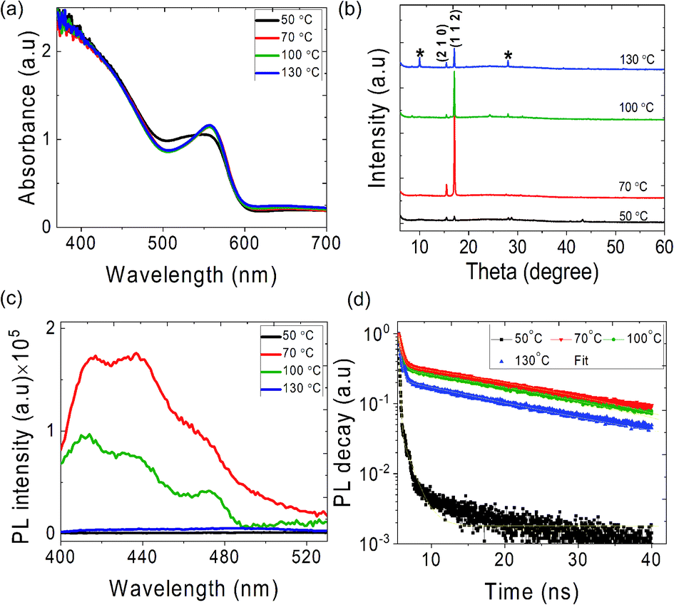
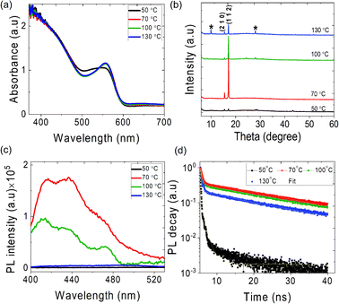
The ATBiI4 films were deposited on glass and compact (c)-TiO2 deposited Fluorine doped tin oxide (FTO) coated glass substrates and annealed at different temperatures from 50–130 °C. The schematic of the experimental steps, crystal structure of ATBiI4 and photograph of a fabricated solar cell are shown in Fig. S1.† The deposition parameters for film formation and details of characterization are given in the Experimental section. Fig. 1 shows the morphology of ATBiI4 films on c-TiO2/FTO along with cross-sectional view of a typical solar cell consisting of ATBiI4 absorber film annealed at 70 °C. The films annealed at 50 °C shows the morphology with flake-like features scattered on the surface that are attributed to unreacted BiI321,34 due to insufficient annealing temperature and supported by XRD measurements as discussed later. Upon increasing the annealing temperature to 70 °C, most of the BiI3 has been utilised to form ATBiI4 and the surface appears to be comparatively smoother, however, some pinholes are observed. Further increasing the annealing temperature to 100 °C, BiI3 features re-appears on the surface possibly as a result of decomposition of ATBiI4 into ATI and BiI3. The morphology of the 130 °C annealed film is not clear as decomposed ATI accumulated on the surface leading to charging effects during SEM measurements. The cross-sectional SEM image of a typical ATBiI4 solar cell with the device architecture FTO/c-TiO2/ATBiI4/PTAA/Ag is shown in Fig. 1(e), in which ATBiI4 film has the thickness of ∼240 nm. The optical absorption and X-ray diffractograms of the ATBiI4 films prepared at different annealing temperatures are shown in Fig. 2(a) and (b), respectively. All the films show wide absorption in the visible region with absorption onset at around 600 nm, an excitonic peak around 554 nm and broad absorption peak in the UV region. The XRD pattern of the 50 °C annealed film shows poor crystallinity in agreement with surface morphology observed in SEM. The film annealed at 70 °C shows dominant peak at 2θ = 17.01 degrees along with a peak at 2θ = 15.4 degrees corresponding to (112) and (210) crystallographic planes of the orthorhombic phase.30 Upon further increasing the annealing temperature, these dominant peaks become weaker and additional peaks corresponding to the secondary BiI3 phase (indexed by ‘*’ symbol for 130 °C annealed sample) are observed. In addition, the dominant peak shifts toward lower angle for high temperature annealed films [Fig. S2(a)†] due to lattice distortion. A closer look at individual XRD profile shown in Fig. S2(b)† clearly indicates that the films prepared at 50 °C, 100 °C and 130 °C have dominant peaks corresponding to BiI3 phase arising due to unreacted material or decomposition effect, which are consistent with the SEM images. However, this effect is not distinguishable from the UV absorption spectra as the orthorhombic phase with preferred (1 1 2) orientation is present in all the films, and is responsible for the main absorption.
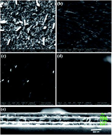 |
| | Fig. 1 SEM surface images of the ATBiI4 films annealed at (a) 50 °C, (b) 70 °C, (c) 100 °C and (d) 130 °C. (e) Cross sectional image of the solar cell with 70 °C annealed ATBiI4. | |
 |
| | Fig. 2 (a) Optical absorption spectra, (b) XRD pattern, (c) PL spectra and (d) TRPL spectra of ATBiI4 films on glass substrates annealed at different temperature. | |
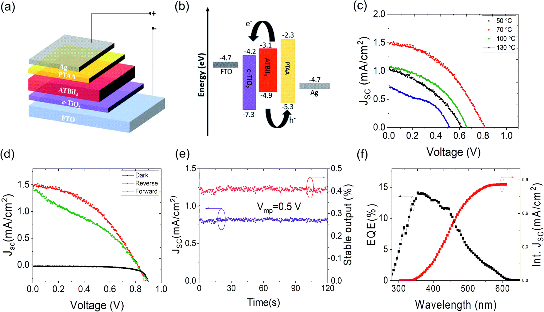
To understand the charge carrier recombination dynamics, photoluminescence (PL) and time resolved PL (TRPL) measurements were carried out on the ATBiI4 films annealed at different temperatures. Fig. 2(c) shows the PL spectra of the ATBiI4 films excited at 350 nm. The emission from the 50 °C annealed film is not well defined as a result of poor crystallinity while the film annealed at 70 °C exhibits a broad emission with multiple peaks centred at 416 nm, 437 nm and 471 nm corresponding to broad absorption in the UV region. A minor emission also observed at 572 nm corresponding to absorption excitonic peak as shown in Fig. S3(b).† The emission profile remains same for the 100 °C annealed film and becomes poor for 130 °C annealed film. An enlarged view of the PL from 50 °C and 130 °C annealed films [Fig. S3(a)†] shows the poor emission intensity which can be correlated to the poor crystallinity of those films. The 70 °C annealed ATBiI4 film deposited on glass and ETL (c-TiO2/FTO) are shown in Fig. S3(b)† in which quenching of PL emission is observed for ETL substrate as a result of fast charge carrier extraction to TiO2. Luminescence decay curves of the ATBiI4 films deposited on glass substrate are shown in Fig. 2(d). The decay curves, except for the 50 °C annealed film, can be fitted with two exponential functions with one decay component associated with the fast surface radiative recombination decay (τ1) and another one with the slow bulk radiative recombination decay (τ2).35 Table S1† shows the decay components of the different films on glass substrates. The average life time of the ATBiI4 films were calculated using the relation (A1τ1 + A2τ2)/(A1 + A2),36,37 where τ and A are the decay and amplitude component, respectively. For 50 °C annealed film, three exponential functions were used to fit the curve. The 70 °C annealed film exhibits average decay time (τavg) of 8.07 ns (τ1 = 0.45 ns and τ2 = 32.07 ns) owing to improved crystalline quality. The films annealed at 50, 100 and 130 °C have τavg of 0.05, 4.66 and 1.35 ns, respectively. The time-resolved luminescence analysis of optimal ATBiI4 films deposited on the ETL surface shows fast surface recombination decay with τ1 decreased to 0.14 ns [Fig. S3(c)†]. The fast decay on the ETL indicates an efficient charge extraction from ATBiI4 to ETL, which can possibly suppress the formation of charge accumulation and hence recombination at the interface.38 The solar cells with a configuration of FTO/c-TiO2/ATBiI4/PTAA/Ag were fabricated with different temperature annealed ATBiI4 absorber films. Fig. 3(a) and (b) show the schematic of the solar cell device and corresponding energy band diagram, respectively. The reverse scan current density–voltage (J–V) plot of the solar cells with different temperature annealed ATBiI4 films are shown in Fig. 3(c) and their photovoltaic parameters are shown in Table 1. As anticipated based on the structural and optical studies, the solar cells incorporated with 70 °C annealed ATBiI4 films exhibit the highest short circuit current density (Jsc) and open-circuit voltage (Voc).
 |
| | Fig. 3 (a) Schematic of the solar cell architecture, (b) energy band diagram of the solar cell, (c) reverse scan J–V plots of the solar cells fabricated with ATBiI4 films annealed at different temperatures, (d) forward and reverse scan J–V plots of the champion device together with dark curve, (e) stabilized power output and Jsc at maximum power point (Vmp = 0.5 V), (f) EQE and integrated Jsc spectra of solar cells with ATBiI4 films annealed at 70 °C. | |
Table 1 Photovoltaic parameters of the ATBiI4 champion solar cells consisting of films annealed at different temperatures
| Annealing temperature (°C) |
V
oc (V) |
J
sc (mA cm−2) |
FF (%) |
PCE (%) |
| 50 |
0.62 |
1.03 |
38.68 |
0.24 |
| 70 |
0.82 |
1.49 |
43.42 |
0.53 |
| 100 |
0.66 |
1.08 |
43.12 |
0.31 |
| 130 |
0.52 |
0.72 |
41.52 |
0.15 |
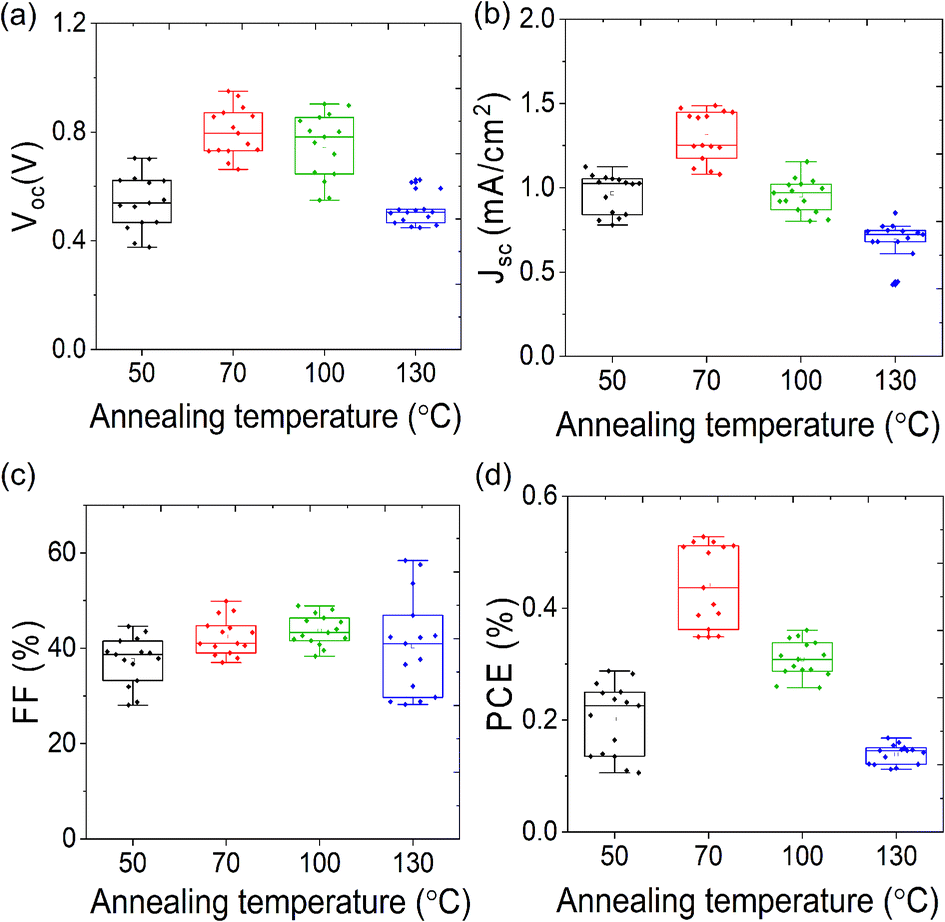
The reverse and forward scan J–V plots along with dark curve of the champion device based on 70 °C annealed ATBiI4 absorber film is shown in Fig. 3(d), which yielded a PCE of 0.53% and 0.39% under reverse and forward scans, respectively. The obtained Voc is higher than that of the reported values based on triple mesoscopic ATBiI4 and AgBiI4 solar cells.27,30 In order to study the PCE judiciously, the best performing device was further biased at its maximum power point (Vmp = 0.5 V) over the period of 120 seconds. As shown in Fig. 3(e), the stable Jsc and PCE of the device are close to that of the values obtained from the J–V plots. The reverse and forward scan plot of 50 °C, 100 °C and 130 °C annealed ATBiI4 films with stable output are shown in Fig. S4(a)–(c).†Fig. 3(f) shows the external quantum efficiency (EQE) spectra and corresponding integrated Jsc curve. The device exhibits maximum EQE of ∼12% at around 400 nm and the integrated Jsc of 0.86 mA cm−2. The EQE spectrum further infers that the 1 sun solar spectrum cannot be fully utilized by ATBiI4 absorber layer, rather blue and near-UV regions can be effectively utilized for energy harvesting. The EQE spectra of other devices are shown in Fig. S5,† which are consistent with J–V plots. The statistical distribution of the photovoltaic metrics from 15 devices fabricated from different temperature annealed absorber are shown in Fig. 4, which reveals a good reproducibility of the ATBiI4 solar cells. The photovoltaic enhancement of the best performing device can be mainly attributed to the phase pure and highly crystalline ATBiI4 films formed by annealing at 70 °C. The best performing device based on 70 °C annealed film was stored under ambient condition (RH: 35–40% and temperature of 20–24 °C) to test aging stability. The J–V plot of the ambient stored device tested over the period of 30 days is shown in Fig. S6† and the device retained ∼60% of its initial PCE.
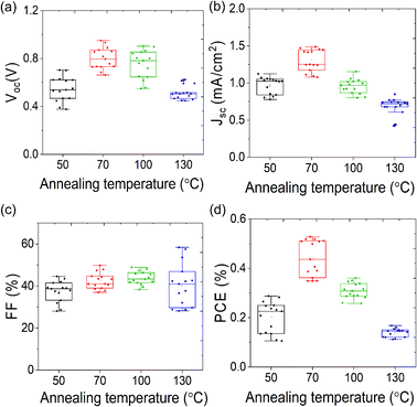 |
| | Fig. 4 Box plot showing the statistical distribution of the device parameters (a) Voc, (b) Jsc, (c) FF and (d) PCE for solar cells with different temperature annealed ATBiI4 absorber films. | |
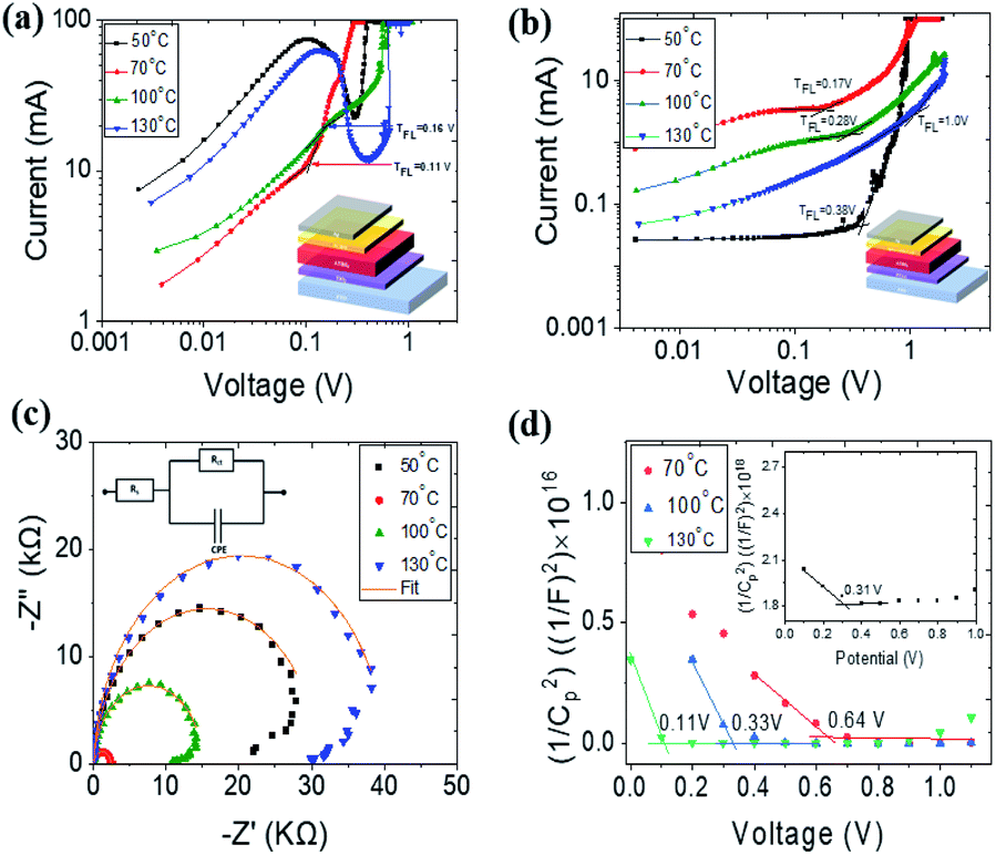
To obtain charge carrier trap densities, we performed space charge limited current (SCLC) method based on electron and hole only devices by measuring J–V characteristics under dark. The SCLC plots of the devices with ETL and HTL only device configurations are shown in Fig. 5(a) and (b). A clear transition from linear (ohmic region) to trap-filled limited (VTFL) and SCLC regions are observed for devices based on 70 °C and 100 °C annealed films with VTFL of 0.11 V and 0.16 V, respectively. For devices based on films annealed at 50 °C and 130 °C, a clear cut-off region was not observed between the trap-filling and SCLC region which makes the SCLC analysis not feasible. All the HTL only devices showed the clear transition region with the VTFL of 0.38 V, 0.17 V, 0.28 V and 1 V for devices based on films annealed at 50 °C, 70 °C, 100 °C and 130 °C, respectively. The onset voltage of VTFL directly related to the trap density (nt) which can be calculated using the relation nt = 2VTFLεε0/ed2,39 where d is the thickness of the film, e is the electron charge, ε is the dielectric constant and ε0 is the vacuum permittivity. The dielectric constant of ATBiI4 is unknown and thus considered as ∼38 (at room temperature) from the related crystal system.12 For the devices based on films annealed at 70 °C, the nt was calculated to be 2.58 × 1018 cm−3 and 3.99 ×1018 cm−3 for ETL and HTL only devices, respectively, which is approximately 1 order of magnitude higher than that of the MA3Bi2I9 system with the nt value of 5.29 × 1017 cm−3.23 Such a high nt of the ATBiI4 films infers that further improvement with reduced nt can be beneficial for enhanced photovoltaic performance. The nt for all the ETL and HTL only devices are given in Table S2† which indicates that the devices based on films annealed at 70 °C exhibit reduced charge carrier trap densities as a result of better bulk and surface properties, which contributes to increased solar cell performance. The electrochemical impedance measurements (EIS) on ATBiI4 solar cells were carried out over a frequency range of 0.1 Hz to 1 kHz with an ac amplitude of 5 mV under dark. The corresponding Nyquist plot is shown in Fig. 5(c). The observed distinctive semicircle at the high frequency region is usually related to the charge transport resistance at the interface between the ATBiI4/ETL in the device.40,41 From the Nyquist plot, the series resistance (Rs) and the charge transport resistance or contact resistance (Rct) can be extracted by fitting the plot using the equivalent circuit model as shown in the inset of Fig. 5(c). The numerical fitting reveals Rs and Rct of 3.18 Ω and 2.42 kΩ for the device with films annealed at 70 °C. The fitting values of all the devices are summarized in Table S3† where it can be clearly seen that 70 °C based devices show reduced Rct values which allows efficient electron transport from the ATBiI4 layer to c-TiO2 and suppress the interface recombination processes.42 Moreover, except for device with film annealed at 70 °C (magnified view in Fig. S7†), all other devices exhibited negative capacitance loop after Rct region. Literature reported different mechanism for the negative capacitance of the solar cells relating to classical capacitance effect.43,44 Fabregat-Santiago et al.44 directly compared the negative capacitance with reduction in Voc and FF resulting in poor performance of perovskite solar cells. Ebadi et al.45 reported that negative capacitance in perovskite solar cells are due to slow transients in the injected currents and further correlated their appearance with J–V curves measured under dark. They also observed more pronounced negative capacitance when Bi impurity phase was introduced into the perovskite system. In the present study, the ATBiI4 films annealed at 70 °C showed negligible unreacted BiI3 while other films still had unreacted or decomposed BiI3 which might contribute to the observed negative capacitance effects. EIS was further used to analyse the voltage modulation and characterize the built-in potential of ATBiI4 solar cell (VBi) using Mott–Schottky (M–S) relationship. Fig. 5(d) shows the M–S plot of ATBiI4 solar cells with films annealed at 70, 100 and 130 °C and the inset shows the corresponding plot for devices based on 50 °C annealed films. The VBi is defined by the intersection of the 1/C2 curve and horizontal bias axis, which probes into charge accumulation at the interface between the ATBiI4 and TiO2 that affect the potential barrier. The VBi of the device based on 70 °C annealed absorber showed 0.64 V which is much higher than that of the other devices indicating the fast charge collection and reduced carrier accumulation.46 The increased VBi can be attributed to the reduced trap state densities as revealed from the SCLC measurements.
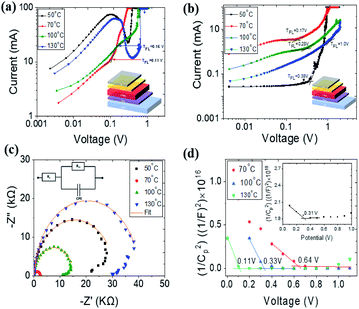 |
| | Fig. 5 Dark I–V plots of the (a) ETL only and (b) HTL only devices with ATBiI4 films annealed at different temperatures; inset shows the corresponding device configuration. (c) Nyquist plot with fitting and (d) Mott–Schottky plot of the ATBiI4 solar cells. | |
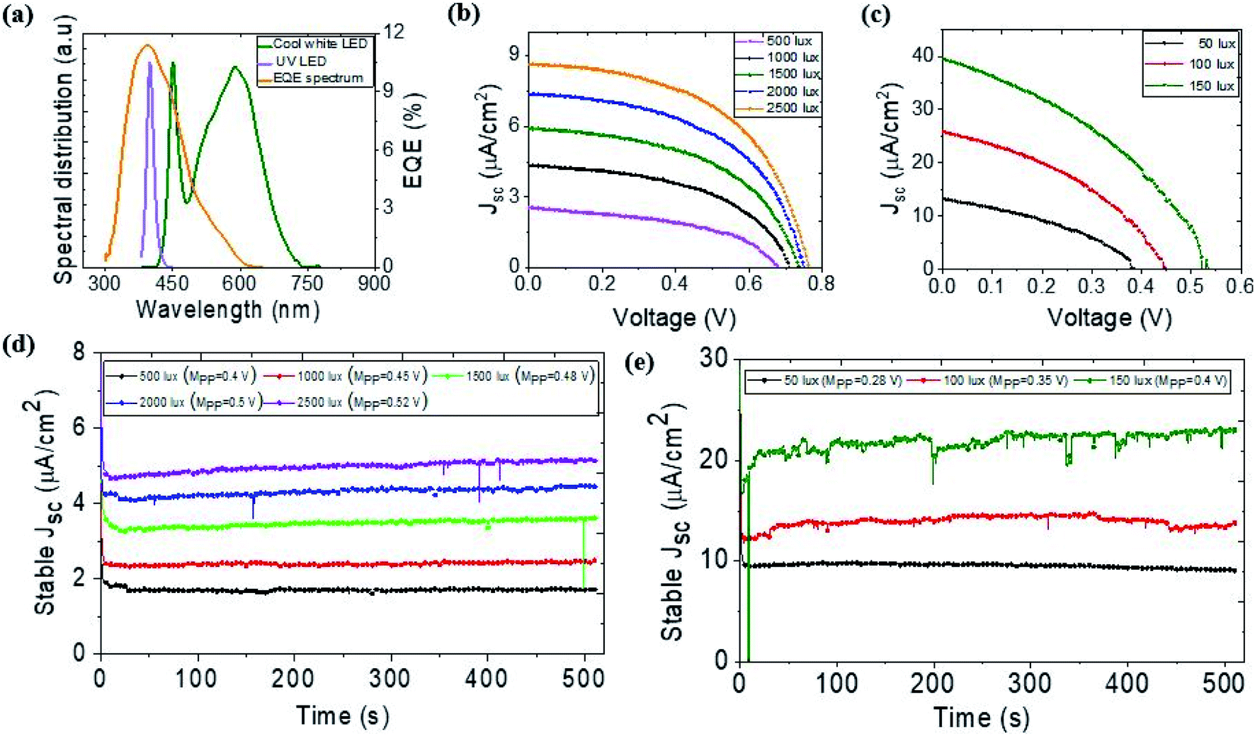
The relative spectral distribution of the 4000 K cool white LED panel and 395–400 nm indoor 9 W UV LED along with EQE spectrum of the ATBiI4 solar cell are shown in Fig. 6(a). While the indoor white LED spectrum partially overlaps the EQE spectrum, the entire UV LED spectrum falls within the EQE spectral range of ATBiI4. Fig. 6(b) shows the J–V plot of the ATBiI4 solar cells tested under different illumination intensity of indoor white LED. The Jsc and Voc of the device linearly increased with increase in incident power. The reverse scan photovoltaic metrics of the champion ATBiI4 solar cell are tabulated in Table 2. The stabilized Jsc of the device biased at maximum power point is shown in Fig. 6(d). For the typical office indoor lighting of 500 lux with an incident power (Pin) of 0.15 mW cm−2, the device yields a PCE of 0.54% and generates a maximum power output of 81.75 μW cm−2. It can be assumed that a mini module formed by connecting few devices can be sufficient to power up smart electronic devices that require microwatt power.47 Further, the devices were tested under a 9 W UV LED lamp. Fig. 6(c) shows the J–V (reverse scan) plot of the device tested under 50, 100 and 150 lux and the corresponding photovoltaic parameters are summarized in Table 3. We note that the Pin for UV light corresponding to the minimum light intensity is much higher than that of the cool white LED as UV light has high-energy photons, which results in high Jsc. The PCE of the device measured under 50, 100 and 150 lux are 0.14, 0.16 and 0.21%, respectively. Although the PCE is not improved substantially with increasing Pin, the power output increased markedly. The maximum power output of 8.07 μW cm−2 obtained from 150 lux can be sufficient to power up some sensors and IoT devices when integrated as a mini module. The stabilized Jsc of the device biased at Vmp under different light intensities over the period of 500 seconds are shown in Fig. 6(e). The fluctuations in the stable output with increasing light intensity results from the burn-in damage induced by high energy UV photons. We further noticed that the device is not highly stable after UV photon irradiation for prolonged time and some visible burn-in features were observed in the device, which could be addressed via interface engineering.
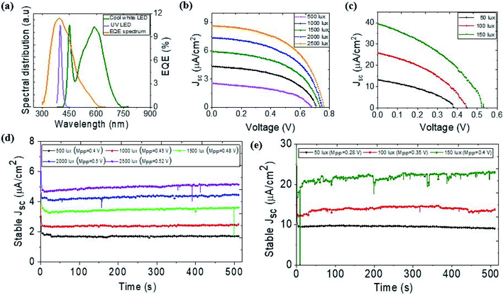 |
| | Fig. 6 (a) Relative spectral distribution of cool white LED and UV LED along with EQE spectrum of ATBiI4 solar cell. J–V plots of the solar cell with ATBiI4 films annealed at 70 °C measured under different illumination intensity of (b) cool white LED and (c) near-UV LED (395–400 nm). Stable Jsc of the device biased at Vmp measured under different illumination intensity of (d) cool white LED and (e) near-UV LED (395–400 nm). | |
Table 2 Photovoltaic metrics of the ATBiI4 solar cells measured under different intensity of 4000 K white LED panel
| Intensity (lux) |
P
in (μW cm−2) |
FF (%) |
J
sc (μA cm−2) |
V
oc (V) |
PCE (%) |
P
max (μW cm−2) |
| 500 |
150.45 |
47.04 |
2.55 |
0.68 |
0.54 |
81.75 |
| 1000 |
300.94 |
50.55 |
4.35 |
0.71 |
0.52 |
156.32 |
| 1500 |
450.21 |
51.09 |
5.91 |
0.74 |
0.50 |
222.60 |
| 2000 |
600.52 |
52.14 |
7.35 |
0.75 |
0.48 |
287.42 |
| 2500 |
750.56 |
52.66 |
8.63 |
0.76 |
0.46 |
347.00 |
Table 3 PV performance metrics of the ATBiI4 solar cells tested under near-UV LED (395–400 nm) light
| Intensity (lux) |
P
in (μW cm−2) |
FF (%) |
J
sc (μA cm−2) |
V
oc (V) |
PCE (%) |
P
max (μW cm−2) |
| 50 |
1371.22 |
38.08 |
13.26 |
0.39 |
0.14 |
1.95 |
| 100 |
2781.19 |
39.06 |
25.86 |
0.45 |
0.16 |
4.54 |
| 150 |
3764.42 |
38.15 |
39.59 |
0.53 |
0.21 |
8.07 |
Conclusions
Lead free 2-aminothiazolium bismuth iodide thin films were prepared and comprehensively characterized for their potential to integrate into planar n–i–p configuration solar cells. The films prepared at low temperature of 70 °C showed enhanced properties and are stable. The solar cells with the device architecture of FTO/c-TiO2/ATBiI4/PTAA/Ag were fabricated and tested under different light sources. Accordingly, the ATBiI4 solar cell yielded PCE of 0.53% under 1 sun and retained ∼60% PCE over 30 days stored at ambient conditions. The solar cell tested under indoor white LED panel (cool white, 4000 K) delivered a PCE of 0.54% at 500 lux with the power output of 81.75 μW cm−2. Interestingly, the solar cell tested under indoor 9 W UV LED delivered the power out of 8.07 μW cm−2 with the PCE of 0.21%. This work demonstrates that ATBiI4 solar cells, when integrated as a mini module, can be useful of powering up microwatt energy requiring smart electronic devices.
Experimental
Materials
Except 2-aminothiazolium iodide (ATI), all the materials used in this work were purchased from commercial suppliers, and used as received. These included bismuth(III) iodide (99%, Sigma-Aldrich)), titanium(IV) isopropoxide (99.99%, Sigma-Aldrich), poly[bis(4-phenyl)(2,5,6-trimethylphenyl)amine (M515 PTAA, 99.9%, Ossila), bis(trifluoromethane)sulfonimide lithium salt (Sigma-Aldrich), absolute ethanol (99.8%, Fisher Chemical), hydrochloric acid 37% (HCL, VWR Chemicals), N,N-dimethyl formamide (DMF, 99.8%, Acros Organics), dimethyl sulfoxide (99.7+%, Acros Organics), toluene (99.8%, Sigma-Aldrich), acetonitrile (99.8%, Sigma-Adrich), Zn powder (99.8+%, Acros Organics), Hellmanex III (Sigma-Aldrich), silver pellet (99.99%, Kurt. J. Lesker) and TEC 15 FTO substrates (NSG Pilkington). ATI was synthesized according to the literature.30
Device fabrication
For the fabrication of the solar cells, FTO substrates were patterned using Zn powder and 4 M HCl. The patterned substrates were cleaned in 2% Hellmanex solution in water followed by an ultrasonic bath first with acetone and then isopropanol for 15 min each. The substrates were further cleaned with oxygen plasma treatment for 10 min. Then, 254 μl titanium(IV) isopropoxide solution dissolved in 2 ml absolute ethanol and 35 μl of 2 M HCL, was spin-coated on the cleaned FTO substrates for 45 seconds at 2000 rpm followed by annealing at 100 °C in air for 10 min. The substrates were further sintered at 500 °C for 30 minutes to form compact TiO2 film (c-TiO2). The TiO2 substrates were then plasma cleaned for 10 minutes and transferred to the nitrogen filled glove box. ATBiI4 precursor solution was prepared by mixing 398 mg of BiI3 and 114 mg of ATI in 7:3 DMF/DMSO solvent and stirred for an hour at 65 °C. The hot precursor solution was spin coated on the TiO2 coated substrate at 3000 rpm for 60 seconds and allowed to nucleate at room temperature in a closed Petri dish for 10 minutes. The substrates were then annealed at different temperatures range from 50 to 130 °C for 10 minutes to obtain the ATBiI4 films. To deposit hole transport layer (HTL), 10 mg PTAA was dissolved in 1 ml toluene and then doped with 5 μl of lithium salt (520 mg ml−1 in acetonitrile). The PTAA solution was spin coated at 3000 rpm for 30 seconds. Finally, silver electrodes were thermally evaporated through a shadow mask at 5 × 10⁻⁷ mbar to complete the device.
Characterization
ATBiI4 film surface and solar cell cross-section were imaged using the field-emission scanning electron microscope (FE-SEM, FEI Quanta 250 FEG). The optical absorption of the films was measured using UV-vis spectroscopy (UNICAM UV-300). The XRD measurements were performed at room temperature on a Bruker D2 Phaser system using monochromatic Cu Kα radiation with a wavelength of 1.5406 Å. The samples were scanned in the range 5–80° and an increment of 0.04° on the 2θ scale. The substrates were set to a rotation speed of 8 rpm throughout the measurement. Photoluminescence (PL) measurements were done using Horiba Fluorolog 3-22 with xenon lamp at an excitation wavelength of 350 nm. TRPL measurements were done using Horiba Deltaflex TCSPC lifetime fluorometer with 370 nm Horiba NanoLED source. The PL decay time was determined by fitting the curve using Origin pro software. The electrochemical impedance spectroscopic measurements were performed using AUTOLAB PGSTAT 302N and FRA32M. External quantum efficiency (EQE) spectrum was taken using Bentham (PVE300) in transformer mode. Silicon reference diode was used for calibration.
Current density–voltage (J–V) characterizations
The current–voltage measurements were carried out using Ossila I–V kit. For 1 sun measurement, the solar spectrum at AM 1.5 was simulated with a xenon lamp and filters (Oriel Sol 1A, Class ABB, 94021A) with the measured intensity at 100 mW cm−2. The illumination intensity was calibrated using reference Si solar cell (Newport, 91150V). For indoor LED measurement, 4000 K cool white LED panel were used. ILT350 spectrophotometer was used to measure the light intensity, incident power, and related spectral distribution of the LED panel. These were crosschecked with standard calculations reported elsewhere.48 For measurement under UV-LED, a low power (9 W) A60 UV LED lamp (TBE lighting) with the wavelength of 395–400 nm was used as a source. For all the light sources, current density versus voltage (J–V) curves of the resulting devices were acquired in both forward-scan (FS; −0.2 to 1.2 V) and reverse scan (RS: 1.2 to −0.2) with the scan speed of ∼80 mV s−1. The active area of the devices is 0.0256 cm2 determined by the standard aperture mask.
Author contributions
VA designed, carried out and analysed most of the practical work and drafted the manuscript. FG setup the indoor light measurements. RK carried out EIS measurements, TL designed and synthesized 2-aminothiazolium iodide supervised by NR, and MA assisted in PL and TRPL measurements. AI directly supervised all the work and helped in results interpretation. AI, NR, and YC all provided inputs in the manuscript.
Conflicts of interest
There are no conflicts to declare.
Acknowledgements
Aruna Ivaturi would like to greatly acknowledge UK Research and Innovation (UKRI), Engineering and Physical Sciences Research Council (EPSRC) for the Fellowship grant (EP/P011500/1); EPSRC ECR Capital Equipment grant (EPS0179171) and ScotCHEM for funding IPCE setup.
References
- https://www.nrel.gov/pv/assets/pdfs/best-research-cell-https://www.nrel.gov/pv/assets/pdfs/best-research-cell-efficiencies.20200406.pdf, rev. 04-06-2020.
- S. Gholipour and M. Saliba, Small, 2018, 14, 1802385 CrossRef PubMed.
- H. S. Jung and N.-G. Park, Small, 2015, 11, 10–25 CrossRef CAS PubMed.
- Y. Rong, Y. Hu, A. Mei, H. Tan, M. I. Saidaminov, S. I. Seok, M. D. McGehee, E. H. Sargent and H. Han, Science, 2018, 361, eaat8235 CrossRef PubMed.
- L. Meng, J. You and Y. Yang, Nat. Commun., 2018, 9, 5265 CrossRef CAS PubMed.
- K. Ahmad, P. Kumar and S. M. Mobin, ChemElectroChem, 2020, 7, 946–950 CrossRef CAS.
- K. Ahmad and S. M. Mobin, ACS Omega, 2020, 5, 28404–28412 CrossRef CAS PubMed.
- I. Kopacic, B. Friesenbichler, S. F. Hoefler, B. Kunert, H. Plank, T. Rath and G. Trimmel, ACS Appl. Energy Mater., 2018, 1, 343–347 CrossRef CAS.
- F. Hao, C. C. Stoumpos, D. H. Cao, R. P. H. Chang and M. G. Kanatzidis, Nat. Photonics, 2014, 8, 489–494 CrossRef CAS.
- M. H. Kumar, S. Dharani, W. L. Leong, P. P. Boix, R. R. Prabhakar, T. Baikie, C. Shi, H. Ding, R. Ramesh, M. Asta, M. Graetzel, S. G. Mhaisalkar and N. Mathews, Adv. Mater., 2014, 26, 7122–7127 CrossRef CAS PubMed.
- L. Serrano-Lujan, N. Espinosa, T. T. Larsen-Olsen, J. Abad, A. Urbina and F. C. Krebs, Adv. Energy Mater., 2015, 5, 1501119 CrossRef.
- M. E. Kamminga, A. Stroppa, S. Picozzi, M. Chislov, I. A. Zvereva, J. Baas, A. Meetsma, G. R. Blake and T. T. Palstra, Inorg. Chem., 2017, 56, 33–41 CrossRef CAS PubMed.
- I. Turkevych, S. Kazaoui, E. Ito, T. Urano, K. Yamada, H. Tomiyasu, H. Yamagishi, M. Kondo and S. Aramaki, ChemSusChem, 2017, 10, 3754–3759 CrossRef CAS PubMed.
- Z. Wang, B. L. Lei, X. H. Xia, Z. B. Huang, K. P. Homewood and Y. Gao, J. Phys. Chem. C, 2018, 122, 2589–2595 CrossRef CAS.
- S. Attique, N. Ali, S. Ali, R. Khatoon, N. Li, A. Khesro, S. Rauf, S. Yang and H. Wu, Adv. Sci., 2020, 7, 1903143 CrossRef CAS PubMed.
- K. Ahmad, S. N. Ansari, K. Natarajan and S. M. Mobin, ACS Appl. Energy Mater., 2018, 1, 2405–2409 CrossRef CAS.
- B. W. Park, B. Philippe, X. Zhang, H. Rensmo, G. Boschloo and E. M. Johansson, Adv. Mater., 2015, 27, 6806–6813 CrossRef CAS PubMed.
- K. Ahmad, P. Kumar and S. M. Mobin, Chem.–Asian J., 2020, 15, 2859–2863 CrossRef CAS PubMed.
- M. B. Johansson, H. Zhu and E. M. Johansson, J. Phys. Chem. Lett., 2016, 7, 3467–3471 CrossRef CAS PubMed.
- T. Singh, A. Kulkarni, M. Ikegami and T. Miyasaka, ACS Appl. Mater. Interfaces, 2016, 8, 14542–14547 CrossRef CAS PubMed.
- C. Lan, J. Luo, S. Zhao, C. Zhang, W. Liu, S. Hayase and T. Ma, J. Alloys Compd., 2017, 701, 834–840 CrossRef CAS.
- S. S. Mali, H. Kim, D. H. Kim and C. K. Hong, ChemistrySelect, 2017, 2, 1578–1585 CrossRef CAS.
- C. Ran, Z. Wu, J. Xi, F. Yuan, H. Dong, T. Lei, X. He and X. Hou, J. Phys. Chem. Lett., 2017, 8, 394–400 CrossRef CAS PubMed.
- Z. Zhang, X. Li, X. Xia, Z. Wang, Z. Huang, B. Lei and Y. Gao, J. Phys. Chem. Lett., 2017, 8, 4300–4307 CrossRef CAS PubMed.
- S. M. Jain, D. Phuyal, M. L. Davies, M. Li, B. Philippe, C. De Castro, Z. Qiu, J. Kim, T. Watson, W. C. Tsoi, O. Karis, H. Rensmo, G. Boschloo, T. Edvinsson and J. R. Durrant, Nano Energy, 2018, 49, 614–624 CrossRef CAS.
- F. Bai, Y. Hu, Y. Hu, T. Qiu, X. Miao and S. Zhang, Sol. Energy Mater. Sol. Cells, 2018, 184, 15–21 CrossRef CAS.
- C. J. Lu, J. Zhang, H. R. Sun, D. G. Hou, X. L. Gan, M. H. Shang, Y. Y. Li, Z. Y. Hu, Y. J. Zhu and L. Y. Han, ACS Appl. Energy Mater., 2018, 1, 4485–4492 CrossRef CAS.
- F. He, Q. Wang, W. Zhu, D. Chen, J. Zhang, C. Zhang and Y. Hao, Solid-State Electron., 2021, 176, 107950 CrossRef CAS.
- D. M. Fabian and S. Ardo, J. Mater. Chem. A, 2016, 4, 6837–6841 RSC.
- T. Li, Q. Wang, G. S. Nichol, C. A. Morrison, H. Han, Y. Hu and N. Robertson, Dalton Trans., 2018, 47, 7050–7058 RSC.
- Y. Zhang, F. F. Tirani, P. Pattison, K. Schenk-Joss, Z. Xiao, M. K. Nazeeruddin and P. Gao, Dalton Trans., 2020, 49, 5815–5822 RSC.
- T. Li, Y. Hu, C. A. Morrison, W. Wu, H. Han and N. Robertson, Sustainable Energy Fuels, 2017, 1, 308–316 RSC.
- W. Shockley and H. J. Queisser, J. Appl. Phys., 1961, 32, 510–519 CrossRef CAS.
- M. B. Johansson, B. Philippe, A. Banerjee, D. Phuyal, S. Mukherjee, S. Chakraborty, M. Cameau, H. Zhu, R. Ahuja, G. Boschloo, H. Rensmo and E. M. J. Johansson, Inorg. Chem., 2019, 58, 12040–12052 CrossRef CAS PubMed.
- S.-G. Kim, J. Chen, J.-Y. Seo, D.-H. Kang and N.-G. Park, ACS Appl. Mater. Interfaces, 2018, 10, 25372–25383 CrossRef CAS PubMed.
- Y. Guo, J. Ma, H. Lei, F. Yao, B. Li, L. Xiong and G. Fang, J. Mater. Chem. A, 2018, 6, 5919–5925 RSC.
- Y. Guo, H. Lei, L. Xiong, B. Li and G. Fang, J. Mater. Chem. A, 2018, 6, 2157–2165 RSC.
- S. Jia, J. Wang and L. Zhu, J. Mater. Sci.: Mater. Electron., 2019, 30, 2057–2066 CrossRef CAS.
- J. Xie, K. Huang, X. Yu, Z. Yang, K. Xiao, Y. Qiang, X. Zhu, L. Xu, P. Wang, C. Cui and D. Yang, ACS Nano, 2017, 11, 9176–9182 CrossRef CAS PubMed.
- M. Zou, X. Xia, Y. Jiang, J. Peng, Z. Jia, X. Wang and F. Li, ACS Appl. Mater. Interfaces, 2019, 11, 33515–33524 CrossRef CAS PubMed.
- H. Zhang, T. Stubhan, N. Li, M. Turbiez, G. J. Matt, T. Ameri and C. J. Brabec, J. Mater. Chem. A, 2014, 2, 18917–18923 RSC.
- C. Tian, E. Castro, G. Betancourt-Solis, Z. Nan, O. Fernandez-Delgado, S. Jankuru and L. Echegoyen, New J. Chem., 2018, 42, 2896–2902 RSC.
- M. T. Khan, P. Huang, A. Almohammedi, S. Kazim and S. Ahmad, iScience, 2021, 24, 102024 CrossRef CAS PubMed.
- F. Fabregat-Santiago, M. Kulbak, A. Zohar, M. Vallés-Pelarda, G. Hodes, D. Cahen and I. Mora-Seró, ACS Energy Lett., 2017, 2, 2007–2013 CrossRef CAS.
- F. Ebadi, N. Taghavinia, R. Mohammadpour, A. Hagfeldt and W. Tress, Nat. Commun., 2019, 10, 1574 CrossRef PubMed.
- T. Bu, J. Li, F. Zheng, W. Chen, X. Wen, Z. Ku, Y. Peng, J. Zhong, Y.-B. Cheng and F. Huang, Nat. Commun., 2018, 9, 4609 CrossRef PubMed.
- C. J. Traverse, R. Pandey, M. C. Barr and R. R. Lunt, Nat. Energy, 2017, 2, 849–860 CrossRef.
- A. Venkateswararao, J. K. W. Ho, S. K. So, S.-W. Liu and K.-T. Wong, Mater. Sci. Eng., R, 2020, 139, 100517 CrossRef.
Footnote |
| † Electronic supplementary information (ESI) available: ATBiI4 film formation, crystal structure, XRD patterns, J–V curves, EQE spectra, PL and TRPL spectra. See https://doi.org/10.1039/d1se02017j |
|
| This journal is © The Royal Society of Chemistry 2022 |
Click here to see how this site uses Cookies. View our privacy policy here. 
 Open Access Article
 This Open Access Article is licensed under a
  a,
Fraser
Gun
a,
Fraser
Gun