
 Open Access Article
 This Open Access Article is licensed under a
 Creative Commons Attribution 3.0 Unported Licence
Efficient bandgap widening in co-evaporated MAPbI3 perovskite†
Herlina Arianita
Dewi
a,
Jia
Li
a,
Enkhtur
Erdenebileg
a,
Hao
Wang
a,
Michele
De Bastiani‡
 b,
Stefaan
De Wolf
b,
Nripan
Mathews
*ac,
Subodh
Mhaisalkar
*ac and
Annalisa
Bruno
*a
b,
Stefaan
De Wolf
b,
Nripan
Mathews
*ac,
Subodh
Mhaisalkar
*ac and
Annalisa
Bruno
*a
aEnergy Research Institute @ NTU (ERI@N), Nanyang Technological University, 637553, Singapore. E-mail: annalisa@ntu.edu.sg; subodh@ntu.edu.sg; nripan@ntu.edu.sg
bKAUST Solar Center (KSC), Physical Sciences and Engineering Division (PSE), King Abdullah University of Science and Technology (KAUST), Thuwal, 23955-6900, Kingdom of Saudi Arabia
cSchool of Materials Science & Engineering, Nanyang Technological University, 639798, Singapore
First published on 13th April 2022
Abstract
Co-evaporated perovskite solar cells (PSCs) have demonstrated outstanding properties, such as great scalability, intrinsic stability, high-power conversion efficiency (PCE), and fabrication adaptability even on rough surfaces. At present, MAPbI3 is the most used co-evaporated perovskite due to the complexity of forming multi-component compositions by thermal evaporation. Even though PSCs with high PCEs have been obtained, the MAPbI3 bandgap (∼1.60 eV) is not ideal for multijunction devices. In this work, we propose a facile method to increase the bandgap of co-evaporated MAPbI3 (∼1.60 eV) through a MABr-based treatment. The best MABr-treated perovskite composition films show a bandgap of 1.66 eV (MAPb(Br0.18I0.82)3) and exhibit good spectral stability under continuous 1-sun illumination at the ambient conditions of 28 °C and 70% relative humidity. This hybrid method works efficiently for thick co-evaporated MAPbI3 films (∼750 nm), which is unusual for hybrid processes. The n-i-p PSCs built from the MAPb(Br0.18I0.82)3 films exhibit a blue-shifted external quantum efficiency and a Voc increase of ∼30 mV as compared to the pure MAPbI3 PSCs, in agreement with the bandgap widening observed in the films. This hybrid method to crete wide bandgap perovskites can be universally applied to MAPbI3 deposited on both flat and textured surfaces and shows great promise for its integration in monolithic tandems.
Introduction
The rapid developments of single-junction perovskite solar cells (PSCs) reaching record power conversion efficiencies (PCE) of 25.5% (ref. 1) over small areas and 18.4% for mini-modules2,3 have driven commercialization interests worldwide in the last few years. The extraordinary perovskite properties, such as low-cost fabrication, defect tolerance, long diffusion length, high absorption coefficient, and efficient charge transfer4–9 further underline the great promise for a variety of perovskite-based optoelectronic devices.10–12 One attractive property lies in the bandgap tunability of perovskites, enabling multi-junction solar cells in combination with low bandgap solar cells (SCs), such as silicon, copper indium gallium selenide (CIGS), organic photovoltaic, or even another lower bandgap perovskite.13–19 By combining the sub-SCs in a tandem configuration, an increase in PCEs beyond each single-junction SCs limit can be achieved.16,20,21 In the tandem configuration, the top PSCs mainly utilize the UV-visible part of the solar spectrum and transmit the infrared components to be harvested by the underlying lower bandgap sub-SC. The perovskite top SC bandgap tuning in the range between 1.66–1.85 eV is necessary to optimally utilize the solar spectrum16,20,22 and then make these SCs more feasible for tandem application, especially with silicon SCs.The most straightforward method to obtain a high-bandgap perovskite (i.e.: Eg > 1.65 eV) is based on composition engineering with mixed iodide/bromide halides23–26 together with the introduction of multiple cations.27–29 In solution-processed perovskites, high-bandgap perovskites can be easily obtained by varying the precursor's composition in the solution. On the other hand, perovskites fabricated by vacuum processes such as thermal evaporation are attracting increasing industrial interest, as the process is low temperature, scalable, and cost-effective and can guarantee a conformal coating on textured surfaces.2,30–36 These features are critical for both large-area perovskite, modules, and monolithic tandem SCs fabrication and in the view of building-integrated photovoltaics.22 Fabrication of high-bandgap evaporated perovskite normally requires multiple co-evaporation sources. Previous reports have shown co-evaporation of single cation methylammonium lead iodide-bromide (MAPb(BrxI1−x)3)37, which already required the use of multiple sources. Co-evaporation processes for more complex compositions with both multi-cation (by incorporation of cesium and formamidinium), as well as multi-halide (iodine and bromine), had also been recently demonstrated.38–40 Despite the successful development of wide bandgap perovskites completely by the evaporation process, the main challenges in adopting these approaches are related to instrumental and operational limitations. Indeed, the availability of dedicated multi-sources thermal evaporators is often limited, and proper control of the individual precursor's rate to obtain perovskites with phase-stable multi-halide compositions can be complex and time-consuming. Different two-step approaches to faster tune the perovskite composition using hybrid deposition processes have been explored by combining thermally evaporated porous templates of lead iodide (PbI2) and/or cesium cations followed by spin coating of organohalide solution.41–45 Two-step methods based on the reaction of the evaporated PbI2 (ref. 46 and 47) or PbBr2 (ref. 48) and organohalide species containing bromine have shown the capability to widen the perovskite bandgap. The limiting factor has been represented by the thickness of the porous lead template that has to be below 400 nm to allow an efficient halide conversion. This represents a stringent limitation in the optimization of the PSCs.46,47 On the other hand, low concentration of MABr treatments has also been proved to be efficient passivation strategies on spin-coated perovskite.49,50 Although, when higher MABr concentrations have been implemented on spin-coated perovskites, the treatments did not improve the performances of the PSCs. So, while MABr treatments are an efficient passivation strategy for spin-coated PSCs, they are not suitable for widening the bandgaps in these perovskites.
In this work, we present an optimized hybrid method to fabricate wider bandgap perovskites based on the MABr interdiffusion effective also for film thicknesses well above 400 nm, which is the limit for the hybrid methods before. We use, for the first time, a co-evaporated MAPbI3 film as a template and a MABr solution-based treatment to create bromine interdiffusion into the films. The advantage of using a thermal co-evaporated perovskite as a template is that this deposition is conformable on rough and textured surfaces. We show that this method can efficiently tune the MAPbI3 film bandgap without affecting the conformal coating of the film on the textured surface. We prove that bromine incorporation can efficiently take place in a 750 nm thick MAPbI3 layer, as demonstrated by a variety of optical and structural techniques as UV-vis absorption, photoluminescence, X-ray diffraction (XRD), X-ray photoelectron spectroscopy (XPS), and scanning electron microscopy (SEM) analysis. Moreover, the n-i-p PSCs incorporating the wide bandgap (∼1.66 eV) MABr-treated- MAPbI3 films as active layers clearly show a blue-shift in their external quantum efficiency (EQE) and an increase in Voc (up to 30 mV) as compared to the standard MAPbI3 PSCs. This hybrid method to widen the perovskite bandgap is extremely attractive for monolithic perovskite/perovskite and perovskite/silicon tandem integration. This method can speed up the screening and optimization process of the perovskite composition, thickness, and bandgap conditions for different configurations or architectures. This method can also be useful for reaching a composition optimization towards the full evaporation process which is time-consuming and requires precise control of each of the precursor rates, and the chamber operating pressure conditions, especially when involving evaporation of organic moieties.
Results and discussion
The 750 nm thick MAPbI3 with PbI2 excess films have been deposited on glass substrates by co-evaporating PbI2 and MAI following the previously reported procedures.2 To shorten the description, the MAPbI3 with PbI2 excess will be written as MAPbI3 only for the following discussion. This thickness has been chosen as it can guarantee the highest performance in our n-i-p co-evaporated PSCs.2,30,35,51,52 The MAPb(BrxI1−x)3 films have been prepared by dropping the MABr solution (with a concentration of 10 mg ml−1 in IPA) on the MAPbI3 film and letting it reacts for a certain time interval (ranging from 1 min to 5 min) before spin-coating the films to remove unreacted MABr/IPA. The 3-steps process is schematized in Fig. 1A.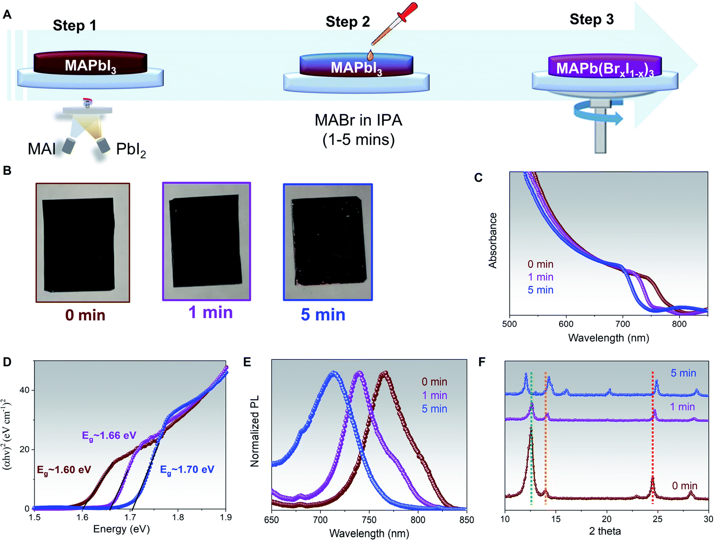 | ||
| Fig. 1 Bandgap tuning of the co-evaporated MAPbI3 + MABr perovskite. (A) Schematic workflow of the hybrid process; (B) photographs of the as-deposited MAPbI3 (brown), MAPbI3 + MABr samples with 1 min (purple), and 5 min (blue) reaction time. (C) Absorbance, (D) Tauc plot, (E) steady-state photoluminescence, and (F) XRD patterns of the MAPbI3 + MABr perovskite films for different MABr timing treatment using an incident angle of 2°. The green, orange, and red lines represent PbI2 〈001〉, perovskite 〈110〉, and perovskite 〈202〉 peaks' positions for MAPbI3. | ||
The pictures of the films before and after 1- and 5 minutes reaction times are reported in Fig. 1B. A negligible color change can be observed for the films treated for 1 min with MABr, while prolonged exposure to MABr solution for 5 min resulted in poor film morphology, pinhole formation, and an obvious orange color appearance on the side of the substrate. The successful bandgap tuning is shown in the clear shift in absorbance toward lower wavelengths of the MABr-treated films as compared to the pure MAPbI3, ones, Fig. 1C. The shift of the bandgap in eV can also be observed from the Tauc plots in Fig. 1D. The MAPbI3 film has a bandgap of ∼1.60 eV in agreement with our previous results,2 while the MABr-treated films showed bandgaps of ∼1.66 eV and ∼1.70 eV for 1 min and 5 min treatment, respectively. It has been known that phase segregation tends to occur when bromine concentration is above 0.2 to 1 for MAPb(BrxI1−x)3 composition.37,53 Based on the empirical equation: Eg(x) = 1.57 + 0.39x + 0.33x2, where Eg is the bandgap of perovskite (in eV) and x is the amount of Br, the hybrid perovskite films compositions are estimated as MAPb(Br0.18I0.82)3 and MAPb(Br0.28I0.72)3 for 1 min and 5 min MABr treatment.23,24 Consistent with the shifts in absorption, shifts of 25 and 50 nm in steady-state photoluminescence peak have also been measured for both the 1 min and 5 min MABr-treated films as compared to MAPbI3 peak, Fig. 1E. In Fig. S1,† we show that the use of different MABr concentrations, ranging from 5 to 15 mg ml−1 with 1 min reaction time proved that an identical absorption shift (and bandgap) can be achieved regardless of different MABr concentrations. This result highlights that, for a film with a specific thickness and PbI2 excess, the conversion time is the crucial parameter to determine the final bandgap in this hybrid method, rather than the MABr concentration. We have also investigated the effect of the annealing process on the bandgap shift. In Fig. S2,† we show that a similar absorbance shift can be attained for the 1 min MABr-treated films prepared with and without post-annealing process at 100 °C for 30 minutes, indicating that bromine interdiffusion can still occur even at room temperature.
The MAPbI3 film exhibits two main crystal orientations at 〈110〉 and 〈202〉 directions, with the latter being more dominant as shown by the sharp perovskite peak at 24.5°, and an excess of PbI2 〈001〉, denoted by the 12.5° XRD peak, brown curve Fig. 1F. The as collected XRD pattern of 1 min MABr-treated films, purple curve Fig. 1F, shows few interesting features. First, a significant reduction in the PbI2 peak suggests that the reaction of MABr with the PbI2 excess takes place. Furthermore, the 〈202〉 perovskite peak shifts from 24.5° to 24.7°, while the 〈110〉 perovskite peak becomes more intense and shifts from 14° to 14.2°, as compared to MAPbI3, confirming the incorporation of bromine into perovskite lattice.48 The XRD pattern of 5 min MABr-treated films, blue curve Fig. 1F, also exhibits very distinctive features. A full conversion of excess PbI2 after 5 min MABr treatment is demonstrated from the disappearance of the PbI2 peak, while both the 〈110〉 and 〈202〉 orientation become well defined. As compared with the MAPbI3, the 〈202〉 perovskite peak shifts from 24.5° to 24.9° and the 〈110〉 perovskite peak shows a shift from 14° to 14.3°. Besides, multiple XRD peaks appeared at 12°, 16°, and 20°, suggesting the formation of additional phases or orientation changes related to bromine excess. To confirm that the main perovskite XRD peaks shift is caused by the presence of bromine halide, the co-evaporated MAPbI3 film is treated with MAI solution (10 mg ml−1 MAI in IPA) for 1 minute, Fig. S3.† Similarly, to the MABr-treated film, reduction in PbI2 and higher 〈202〉 perovskite peaks are observed as compared to our pristine MAPbI3, indicating the reaction of MAI with the excess PbI2 inside the film. Indeed, the MAI-treated film shows unshifted peak position for both 〈110〉 and 〈202〉 perovskite orientations, confirming that XRD peak shift is driven by bromine inclusion inside perovskite lattice. A combination of poor perovskite film morphology, unstable phase formation due to higher bromine content, and the additional XRD peaks in 5 min MABr-treated films suggest that this condition is not suitable to reach long-term stability. Hence, subsequent studies are done using the 1 min MABr-treated films and we will refer to these as MAPb(Br0.18I0.82)3. We have also shown that when the same MABr treatment is applied on stoichiometric grown MAPbI3 film with different crystallographic orientations, Fig. S4A,† the shift of the bandgap is just a few nanometres smaller, Fig. S4B and C,† than the one obtained in films with PbI2 excess. The reason behind this effect is that MABr can efficiently react with both the PbI2 and the iodine within the lattice creating a mixed halide perovskite.
To assess the iodine/bromine ratio across the whole film thickness for both MAPbI3 and MAPb(Br0.18I0.82)3, XRD patterns have been measured using different incident angles from 2° to 8°. Indeed, higher incident angles can probe a deeper portion within the perovskite film, as shown in Table S1† and ref. 30. The MAPbI3 film shows, for all incident angles, a dominant 〈202〉 perovskite orientation and a compositional gradient across the whole perovskite thickness, with a higher PbI2 〈001〉 content, on nearby perovskite surface, Fig. 2A, in agreement with what has been observed before.35 In contrast, the MAPb(Br0.18I0.82)3 film shows a higher 〈110〉 peak for all the incident angles as compared to MAPbI3, with a lower PbI2 concentration. Moreover, the 〈110〉 peak appears to be more predominant with the lowest incident angle (2°) indicating that even though MABr can inter-diffuse and react with an excess of PbI2 throughout the whole thickness, the prominent reaction is occurring at the surface, Fig. 2B. The non-normalized XRD spectra taken at different angles are reported in Fig. S5.†
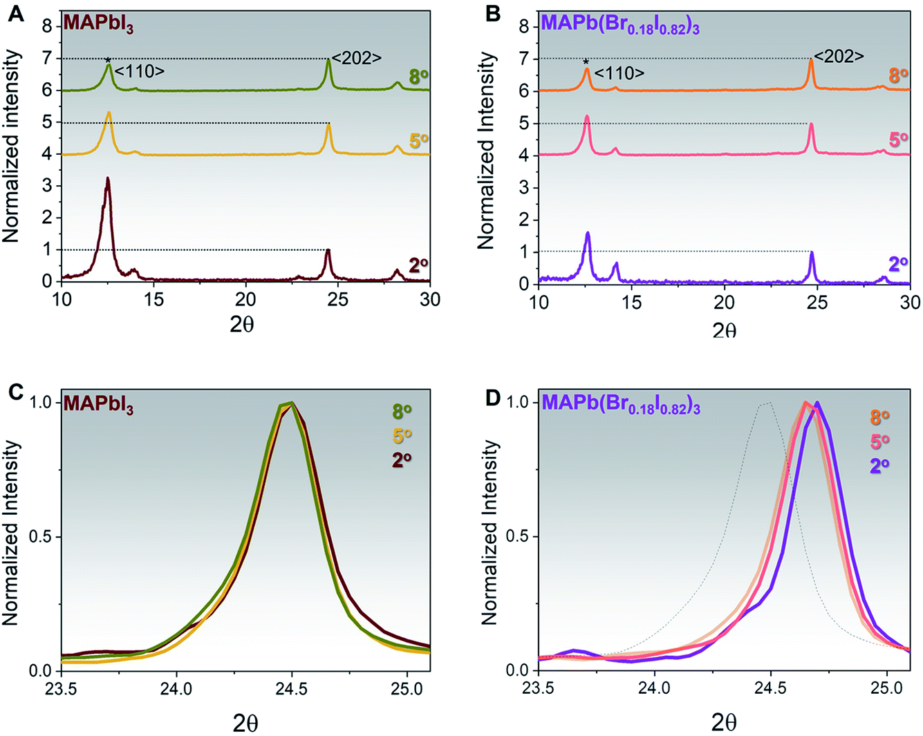 | ||
| Fig. 2 MAPbI3 and MAPb(Br0.18I0.82)3 XRD Patterns. XRD patterns with the incident angle of 2°, 5°, and 8°. The PbI2 peak is defined by *. The XRD patterns are normalized toward the 〈202〉 perovskite peak for each condition. (A) MAPbI3 and (B) MAPb(Br0.18I0.82)3. Zoom-in XRD peaks at the respective 〈202〉 perovskite peak taken from 23.5–25.2° range for (C) MAPbI3 and (D) MAPb(Br0.18I0.82)3, the dotted line is the XRD peak of MAPbI3 as reference. | ||
The zoom-in XRD peaks at the respective 〈202〉 perovskite peak taken from 23.5–25.2° range for both MAPbI3 and MAPb(Br0.18I0.82)3 are shown in Fig. 2C and D. It is indeed shown that as expected the position of the 〈202〉 peak does not shift throughout the thickness for MAPbI3, Fig. 2C. On the other hand, the MAPb(Br0.18I0.82)3 XRD patterns show that the 〈202〉 peak gradually shifts from 24.7° into 24.6°, upon increasing the incident angle from 2° to a higher angle of 5° or 8°, suggesting the presence of a slight bromine gradient with the higher bromine content located near perovskite surface, Fig. 2D. The dotted line in Fig. 2D represents the XRD spectra of MAPbI3 as reference.
The MAPbI3 and MAPb(Br0.18I0.82)3 films' compositions have been also been investigated through FESEM images to correlate the effect of bromine/iodine gradient with the perovskite morphology. The top-view FESEM image of the MAPbI3, Fig. 3A, shows film morphology with small, uniform, and compact perovskite grain sizes and narrow distribution with an average size of 150 nm in agreement with previously reported morphologies for evaporated MAPbI3 films.2,52,54 Also, for pure MAPbI3 the cross-section FESEM image shows a uniform perovskite grain size throughout the whole thickness, Fig. 3B. While for the MAPb(Br0.18I0.82)3 films, Fig. 3C, the FESEM top-view image, shows larger and more inhomogeneous grain sizes upon adopting the bromine halide inside the lattice. The size distribution is wider, and the mean grain size is around 250 nm.
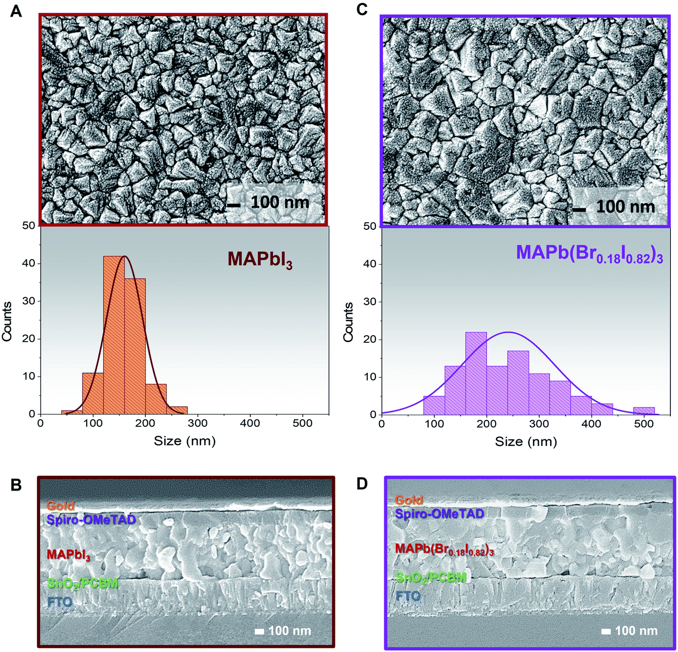 | ||
| Fig. 3 MAPbI3 and MAPb(Br0.18I0.82)3 FESEM images. Top view, grain size distribution histogram (obtained over 100 grains), and cross-section FESEM images of (A and B) MAPbI3 (brown) and (C and D) MAPb(Br0.18I0.82)3 (purple). | ||
On the other hand, a cross-section FESEM image of the treated MABr perovskite solar cells (PSCs) reveals enlarged grains located on the top of perovskite, Fig. 3D. This change in grain size may be due to bromine inclusion, in agreement with the angle-dependent XRD results (Fig. 2). The hybrid method promotes the conversion of excess PbI2 and the iodine inside the lattice with the MABr, and results in bigger grain size, as what it is normally observed during two-step deposition or surface passivation due to the Ostwald ripening process.50,55,56
Further insight into elemental composition and interaction of MABr with MAPbI3 was provided by comparing the XPS spectra of Br, Pb, and I before and after MABr treatment, Fig. S6.† Upon MABr treatment, the signal of Br located at 67.3 eV and 68.3 eV appears for the MAPb(Br0.18I0.82)3 film, Fig. S6A.† In addition, both Pb and I signal are shifted into higher binding energy upon MABr treatment, indicating a modified chemical environment and Pb–Br interactions, Fig. S6B and C.† The surface binding energies (BE) and the atomic concentrations of both MAPbI3 and MAPb(Br0.18I0.82)3 measured using XPS are shown in Table S2.† In the MAPb(Br0.18I0.82)3 the (I + Br)/Pb ratio (calculated from the atomic concentrations in Table S2†) is 2.68 which is smaller than the one observed for the MAPbI3 surface (2.75). The XPS results indeed confirm the reduction of iodide at the surface and that bromine halide is replacing iodide through the interdiffusion process, and it is consistent with the results obtained from the XRD.
Wide bandgap perovskite films containing mixed bromine and iodine contents have shown instability driven by phase separation under continuous illumination.57–59 Accordingly, to monitor the light-induced phase stability of the MAPb(Br0.18I0.82)3 films have been exposed to a continuous 1 sun illumination for 1 hour at room temperature, ∼27 °C, and ambient condition, ∼70% relative humidity (RH), Fig. 4. No significant variations have been observed in either the absorption and steady-state photoluminescence spectra for MAPbI3, used as reference (Fig. 4A and B) and MAPb(Br0.18I0.82)3 (Fig. 4C and D) films. These results validate the photostability of both films and demonstrate the absence of halide segregation for the MAPb(Br0.18I0.82)3 composition, since the chosen composition is still within the phase-stable wide bandgap composition.37,53 In addition, the presence of bromine halide throughout the whole perovskite thickness can also be done by comparing the photoluminescence peak position when illuminated from the perovskite side and glass side, Fig. S7.† For MAPbI3 with excess PbI2, there is no change in PL peak positions at ∼770 nm when excited from either perovskite or glass side, Fig. S7A.† Similarly, the MAPb(Br0.18I0.82)3 film's PL peak position at ∼740 nm does not shift with the different illumination sides indicating successful bromine intercalation throughout 750 nm thickness, Fig. S7B.† The appearance of a slight shoulder shift for MAPb(Br0.18I0.82)3 when taken from the glass side suggests again a minor bromine-gradient through the film thickness. Also, in this case, we have included the MAPbI3 spectra (brown dotted lines) as reference.
 | ||
| Fig. 4 MAPbI3 and MAPb(Br0.18I0.82)3 light stability. UV-vis absorbance and photoluminescence spectra under continuous 1 sun illumination for over 3600 s for (A and B) MAPbI3 and (C and D) MAPb(Br0.18I0.82)3. | ||
PSCs based on both MAPbI3 and MAPb(Br0.18I0.82)3 have been fabricated in the n-i-p configuration using the bilayer SnO2/PCBM as electron transport material (ETM) and Spiro-OMeTAD as hole transport material (HTM), and a gold top contact, as shown in Fig. 5A. With this device structure, the band edge of the external quantum efficiency (EQE) shifts toward lower wavelengths (∼30 nm), indicating successful bandgap tuning, Fig. 5B. Consistently, the PSCs show an average increase in Voc of ∼30 mV, from an average of ∼1.05 to ∼1.08 V, upon bromine inclusion, Fig. 5C, in agreement with the widening of the perovskite bandgap. The statistical distributions of all the photovoltaic parameters (Jsc, FF, and PCE) are reported in Fig. S8A–C.† The champion PCEs for both MAPbI3 and MAPb(Br0.18I0.82)3 PSCs are taken from reverse and the forward direction is shown in Fig. S9.† The PSCs based on MAPb(Br0.18I0.82)3 also show a very promising shelf-life stability with no appreciable losses in PCE when stored under a controlled environment of 30% RH and room temperature. The trend as a function of the time of the statistical distributions of all the photovoltaic parameters is reported in Fig. S10.†
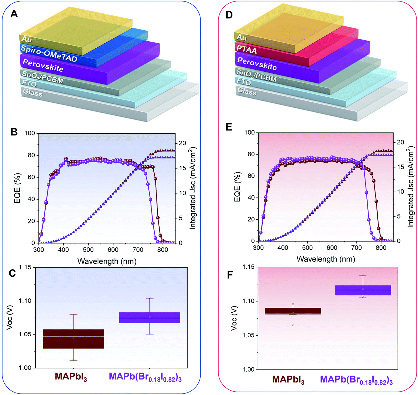 | ||
| Fig. 5 MAPbI3 and MAPb(Br0.18I0.82)3 perovskite solar cells (PSCs) (A) schematic of n-i-p PSCs with Spiro-OMeTAD as HTM, (B) EQE, (C) Voc for MAPbI3 and MAPb(Br0.18I0.82)3. (D) Schematic of n-i-p PSCs with PTAA as HTM, (E) EQE, (F) Voc for MAPbI3 and MAPb(Br0.18I0.82)3. | ||
PSCs based on both MAPbI3 and MAPb(Br0.18I0.82)3 with poly(triaryl amine) (PTAA) HTM have been also fabricated, Fig. 5D. PTAA is chosen as an alternative HTM due to its higher transparency at UV-region as compared to Spiro-OMeTAD, which may be more beneficial for semi-transparent PSCs or tandem integration. A similar wavelength shift of 30 nm has been observed in the EQE spectra, Fig. 5E. An increase in Voc of ∼40 mV (from 1.08 to 1.12 V) has also been observed systematically, Fig. 5F. The photovoltaic parameters (Jsc, FF, and PCE), are reported in Fig. S11A–C.† In this device configuration, the champion PSCs taken from both reverse and forward scan is shown in Fig. S12.† The statistic distribution of the PSCs based on Spiro-OMeTAD and PTAA HTLs for both MAPbI3 and MAPb(Br0.18I0.82)3 are presented in Table S3.† The MAPb(Br0.18I0.82)3 PSCs based on PTAA HTM also exhibits good shelf-life stability, with no appreciable losses in PCE when stored under a controlled environment of 30% RH and room temperature for 300 hours Fig. S13.†
One of the main advantages of the thermal co-evaporation deposition method is the possibility of conformal coating on textured surfaces. As shown from the cross-sectional FESEM, the uniform and conformal coating of co-evaporated MAPbI3 can still be obtained, even by using various silicon pyramidal structures which have a random pyramidal height ranging from 1–3 μm, 3–5 μm, and even 5–7 μm, Fig. S14A–C.† The top-view FESEM taken at low magnification shows the complete coverage of MAPbI3 on a relatively silicon large area, with the different morphologies observed corresponding well with the bare silicon morphologies Fig. S14D–F.† Despite being deposited on a different textured surface, the morphologies of MAPbI3 have remained consistent and comparable with the one deposited on a flat surface, Fig. S15.†
Here we show that this MABr interdiffusion method is efficient also when applied on textured surfaces making it promising for monolithic tandem configuration which requires wide-bandgap perovskites conformal deposition on textured surfaces. Indeed, upon the MABr treatment on the perovskite deposited on silicon with 3–5 μm pyramidal height, there is a negligible change on the conformal coating over the textured surface for both MAPbI3 (Fig. 6A) as compared to MAPb(Br0.18I0.82)3, Fig. 6C. The high magnification cross-sectional morphology shows similar grain structures like the one observed on the flat surfaces with larger grains observed nearby perovskite top surface for both compositions, Fig. 6B and D. The top view FESEM images taken at low magnification reveal no change in perovskite coverage over a textured silicon Fig. S16A and B.†
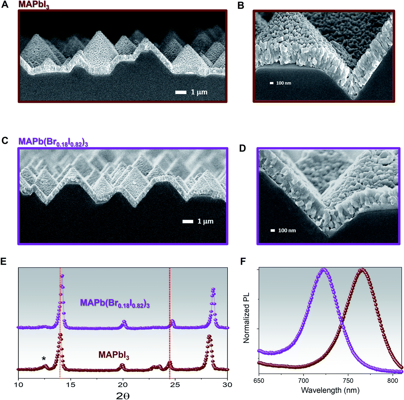 | ||
| Fig. 6 MAPbI3 and MAPb(Br0.18I0.82)3 on textured silicon. cross-sectional FESEM of (A and B) MAPbI3 (brown), (C and D) MAPb(Br0.18I0.82)3 (purple), and (E) XRD of MAPbI3 (brown) and MAPb(Br0.18I0.82)3 (purple) deposited on textured silicon surface with a pyramidal height ∼3–5 μm. The XRD patterns are normalized toward the highest intensity XRD peak for each condition. The orange and red lines represent perovskite orientation at 〈110〉 and 〈202〉 for MAPbI3, while the * represents excess PbI2 in the MAPbI3. (F) Steady-state photoluminescence of MAPbI3 (brown) and MAPb(Br0.18I0.82)3 (purple) deposited on textured silicon surface with a pyramidal height ∼3–5 μm. | ||
The XRD patterns of the co-evaporated MAPbI3 and MAPb(Br0.18I0.82)3 over textured surfaces are shown in Fig. 6E. The deposited MAPbI3 on the textured surface shows a more pronounced preferential orientation in the 〈110〉 direction and less amount of PbI2 peak as compared to the material deposited on a flat substrate. This change in MAPbI3 orientation may be related to the different behaviors of PbI2 and MAI during the co-evaporation process, resulting in more MAI content when deposited in the textured surface as compared to the planar surface, following the previous observation.60 While in the MAPb(Br0.18I0.82)3 film, the excess PbI2 peak disappears and a 0.2° peak shift is observable for both 〈110〉 and 〈202〉 perovskite orientation as compared to the MAPbI3 counterpart, confirming the bromine inclusion based on the reaction of MABr with excess PbI2,Fig. 6E. Fig. 6F also shows the photoluminescence shift toward shorter wavelengths after the MABr treatment, consistently with what has been observed on flat surfaces. These results highlight that the halide interdiffusion method can be efficiently applied for MAPbI3 deposited on both flat and textured surfaces.
Conclusions
In this work, we have shown a facile hybrid method to widen the bandgap of the co-evaporated MAPbI3 perovskite by treating the films with a MABr solution. Indeed a MAPb(Br0.18I0.82)3 film with a bandgap ∼1.66 eV can be obtained by using a co-evaporated MAPbI3 as a template with a bandgap of ∼1.60 eV and tuning MABr reaction time. The n-i-p PSCs integrating MAPb(Br0.18I0.82)3 as the active layer and either Spiro-OMeTAD or PTAA as HTMs, showed a consistent Voc increase up to ∼30–40 mV, as compared to the PSCs based on MAPbI3. This hybrid method is effective in widening the bandgap for MAPbI3 films with thicknesses well above 700 nm and deposited on both flat and textured surfaces pyramidal, showing the potential of forming wide-bandgap perovskite conformally deposited for monolithic tandem integration.Author contributions
HAD and AB had the initial idea and conceived the experiments. HAD developed the method. HAD, LJ, and EE prepared the devices. HAD and WH performed the PL and XRD and FESEM measurements. HAD and AB wrote the first draft. MdB and SW developed the Si solar cells. SM, NM contributed to the conceptual development of the work and AB supervised the work. All the authors revised and commented on the manuscript.Conflicts of interest
Two of the authors N. M. and S. M. are directors of Prominence Photovoltaics Pte, Ltd, a perovskite solar cell commercialization company. The other authors have no conflict of interest to declare.Acknowledgements
This research is supported by the National Research Foundation, Prime Minister's Office, Singapore under the Solar CRP (S18-1176-SCRP) and NRF2018-ITC001-001. The authors wish to thank Dr Teddy for the support with the XRD measurements. This work was partially supported by the King Abdullah University of Science and Technology (KAUST), Office of Sponsored Research (OSR) under award no. OSR-CRG2019-4093.Notes and references
- https://wwwhttps://www.nrel.gov/pv/cell-efficiency.html.
- J. Li, H. Wang, X. Y. Chin, H. A. Dewi, K. Vergeer, T. W. Goh, J. W. M. Lim, J. H. Lew, K. P. Loh, C. Soci, T. C. Sum, H. J. Bolink, N. Mathews, S. Mhaisalkar and A. Bruno, Highly Efficient Thermally Co-evaporated Perovskite Solar Cells and Mini-modules, Joule, 2020, 4(5), 1035–1053 CrossRef CAS
.
- M. Du, X. Zhu, L. Wang, H. Wang, J. Feng, X. Jiang, Y. Cao, Y. Sun, L. Duan, Y. Jiao, K. Wang, X. Ren, Z. Yan, S. Pang and S. Liu, High-Pressure Nitrogen-Extraction and Effective Passivation to Attain Highest Large-Area Perovskite Solar Module Efficiency, Adv. Mater., 2020, 32(47), 2004979 CrossRef CAS PubMed
- K. X. Steirer, P. Schulz, G. Teeter, V. Stevanovic, M. Yang, K. Zhu and J. J. Berry, Defect Tolerance in Methylammonium Lead Triiodide Perovskite, ACS Energy Lett., 2016, 1(2), 360–366 CrossRef CAS
- G. Xing, N. Mathews, S. Sun, S. S. Lim, Y. M. Lam, M. Grätzel, S. Mhaisalkar and T. C. Sum, Long-Range Balanced Electron- and Hole-Transport Lengths in Organic–Inorganic CH3NH3PbI3, Science, 2013, 342(6156), 344–347 CrossRef CAS PubMed
- J. Kang and L.-W. Wang, High defect tolerance in lead halide perovskite CsPbBr3, J. Phys. Chem. Lett., 2017, 8(2), 489–493 CrossRef CAS PubMed
- H. Huang, M. I. Bodnarchuk, S. V. Kershaw, M. V. Kovalenko and A. L. Rogach, Lead Halide Perovskite Nanocrystals in the Research Spotlight: Stability and Defect Tolerance, ACS Energy Lett., 2017, 2(9), 2071–2083 CrossRef CAS PubMed
- S. D. Stranks, G. E. Eperon, G. Grancini, C. Menelaou, M. J. P. Alcocer, T. Leijtens, L. M. Herz, A. Petrozza and H. J. Snaith, Electron-Hole Diffusion Lengths Exceeding 1 Micrometer in an Organometal Trihalide Perovskite Absorber, Science, 2013, 342(6156), 341–344 CrossRef CAS PubMed
- S. De Wolf, J. Holovsky, S.-J. Moon, P. Löper, B. Niesen, M. Ledinsky, F.-J. Haug, J.-H. Yum and C. Ballif, Organometallic Halide Perovskites: Sharp Optical Absorption Edge and Its Relation to Photovoltaic Performance, J. Phys. Chem. Lett., 2014, 5(6), 1035–1039 CrossRef CAS PubMed
- X. Y. Chin, D. Cortecchia, J. Yin, A. Bruno and C. Soci, Lead iodide perovskite light-emitting field-effect transistor, Nat. Commun., 2015, 6, 7383 CrossRef CAS PubMed
- X. Y. Chin, A. Perumal, A. Bruno, N. Yantara, S. A. Veldhuis, L. Martínez-Sarti, B. Chandran, V. Chirvony, A. S.-L. Lo, J. So, C. Soci, M. Grätzel, H. J. Bolink, N. Mathews and S. G. Mhaisalkar, Self-assembled hierarchical nanostructured perovskites enable highly efficient LEDs via an energy cascade, Energy Environ. Sci., 2018, 11, 1770–1778 RSC
- M. D. Birowosuto, D. Cortecchia, W. Drozdowski, K. Brylew, W. Lachmanski, A. Bruno and C. Soci, X-ray Scintillation in Lead Halide Perovskite Crystals, Sci. Rep., 2016, 6, 37254 CrossRef CAS PubMed
- K. Xiao, R. Lin, Q. Han, Y. Hou, Z. Qin, H. T. Nguyen, J. Wen, M. Wei, V. Yeddu, M. I. Saidaminov, Y. Gao, X. Luo, Y. Wang, H. Gao, C. Zhang, J. Xu, J. Zhu, E. H. Sargent and H. Tan, All-perovskite tandem solar cells with 24.2% certified efficiency and area over 1 cm2 using surface-anchoring zwitterionic antioxidant, Nat. Energy, 2020, 5(11), 870–880 CrossRef CAS
- A. Al-Ashouri, E. Köhnen, B. Li, A. Magomedov, H. Hempel, P. Caprioglio, J. A. Márquez, A. B. Morales Vilches, E. Kasparavicius, J. A. Smith, N. Phung, D. Menzel, M. Grischek, L. Kegelmann, D. Skroblin, C. Gollwitzer, T. Malinauskas, M. Jošt, G. Matič, B. Rech, R. Schlatmann, M. Topič, L. Korte, A. Abate, B. Stannowski, D. Neher, M. Stolterfoht, T. Unold, V. Getautis and S. Albrecht, Monolithic perovskite/silicon tandem solar cell with >29% efficiency by enhanced hole extraction, Science, 2020, 370(6522), 1300–1309 CrossRef CAS PubMed
- H. A. Dewi, H. Wang, J. Li, M. Thway, R. Sridharan, R. Stangl, F. Lin, A. G. Aberle, N. Mathews, A. Bruno and S. Mhaisalkar, Highly Efficient Semitransparent Perovskite Solar Cells for Four Terminal Perovskite-Silicon Tandems, ACS Appl. Mater. Interfaces, 2019, 11(37), 34178–34187 CrossRef CAS PubMed
- M. Jošt, L. Kegelmann, L. Korte and S. Albrecht, Monolithic Perovskite Tandem Solar Cells: A Review of the Present Status and Advanced Characterization Methods Toward 30% Efficiency, Adv. Energy Mater., 2020, 10(26), 1904102 CrossRef
- A. Guchhait, H. A. Dewi, S. W. Leow, H. Wang, G. Han, F. B. Suhaimi, S. Mhaisalkar, L. H. Wong and N. Mathews, Over 20% Efficient CIGS-Perovskite Tandem Solar Cells, ACS Energy Lett., 2017, 2(4), 807–812 CrossRef CAS
- X. Chen, Z. Jia, Z. Chen, T. Jiang, L. Bai, F. Tao, J. Chen, X. Chen, T. Liu, X. Xu, C. Yang, W. Shen, W. E. I. Sha, H. Zhu and Y. Yang, Efficient and Reproducible Monolithic Perovskite/Organic Tandem Solar Cells with Low-Loss Interconnecting Layers, Joule, 2020, 4(7), 1594–1606 CrossRef CAS
- Z. Li, S. Wu, J. Zhang, K. C. Lee, H. Lei, F. Lin, Z. Wang, Z. Zhu and A. K. Y. Jen, Hybrid Perovskite-Organic Flexible Tandem Solar Cell Enabling Highly Efficient Electrocatalysis Overall Water Splitting, Adv. Energy Mater., 2020, 10(18), 2000361 CrossRef CAS
- J. Werner, B. Niesen and C. Ballif, Perovskite/Silicon Tandem Solar Cells: Marriage of Convenience or True Love Story? – An Overview, Adv. Mater. Interfaces, 2018, 5(1), 1700731 CrossRef
- G. E. Eperon, M. T. Hörantner and H. J. Snaith, Metal halide perovskite tandem and multiple-junction photovoltaics, Nat. Rev. Chem., 2017, 1(12), 0095 CrossRef CAS
- H. Wang, J. Li, H. A. Dewi, N. Mathews, S. Mhaisalkar and A. Bruno, Colorful Perovskite Solar Cells: Progress, Strategies, and Potentials, J. Phys. Chem. Lett., 2021, 12(4), 1321–1329 CrossRef CAS PubMed
- J. H. Noh, S. H. Im, J. H. Heo, T. N. Mandal and S. I. Seok, Chemical Management for Colorful, Efficient, and Stable Inorganic–Organic Hybrid Nanostructured Solar Cells, Nano Lett., 2013, 13(4), 1764–1769 CrossRef CAS PubMed
- S. A. Kulkarni, T. Baikie, P. P. Boix, N. Yantara, N. Mathews and S. Mhaisalkar, Band-gap tuning of lead halide perovskites using a sequential deposition process, J. Mater. Chem. A, 2014, 2(24), 9221–9225 RSC
-
H. A. Dewi, H. Wang, J. Li, M. Thway, F. Lin, A. G. Aberle, N. Mathews, S. Mhaisalkar and A. Bruno, Four-Terminal Perovskite on Silicon Tandem Solar Cells Optimal Measurements Schemes, 2020, Energy Technology Search PubMed
- H. A. Dewi, H. Wang, J. Li, M. Thway, R. Sridharan, R. Stangl, F. Lin, A. G. Aberle, N. Mathews and A. Bruno, Highly Efficient Semi-Transparent Perovskite Solar Cells for Four Terminal Perovskite-Silicon Tandems, ACS Appl. Mater. Interfaces, 2019, 34178–34187 CrossRef CAS PubMed
- D. P. McMeekin, G. Sadoughi, W. Rehman, G. E. Eperon, M. Saliba, M. T. Hörantner, A. Haghighirad, N. Sakai, L. Korte, B. Rech, M. B. Johnston, L. M. Herz and H. J. Snaith, A mixed-cation lead mixed-halide perovskite absorber for tandem solar cells, Science, 2016, 351(6269), 151–155 CrossRef CAS PubMed
- J. Xu, C. C. Boyd, Z. J. Yu, A. F. Palmstrom, D. J. Witter, B. W. Larson, R. M. France, J. Werner, S. P. Harvey, E. J. Wolf, W. Weigand, S. Manzoor, M. F. A. M. van Hest, J. J. Berry, J. M. Luther, Z. C. Holman and M. D. McGehee, Triple-halide wide-band gap perovskites with suppressed phase segregation for efficient tandems, Science, 2020, 367(6482), 1097–1104 CrossRef CAS PubMed
- K. A. Bush, K. Frohna, R. Prasanna, R. E. Beal, T. Leijtens, S. A. Swifter and M. D. McGehee, Compositional Engineering for Efficient Wide Band Gap Perovskites with Improved Stability to Photoinduced Phase Segregation, ACS Energy Lett., 2018, 3(2), 428–435 CrossRef CAS
- J. Li, H. A. Dewi, H. Wang, J. H. Lew, N. Mathews, S. Mhaisalkar and A. Bruno, Design of Perovskite Thermally Co-Evaporated Highly Efficient Mini-Modules with High Geometrical Fill Factors, Sol. RRL, 2020, 4(12), 2000473 CrossRef CAS
- J. Feng, Y. Jiao, H. Wang, X. Zhu, Y. Sun, M. Du, Y. Cao, D. Yang and S. F. Liu, High-Throughput Large-Area Vacuum Deposition for High-Performance Formamidine-based Perovskite Solar Cells, Energy Environ. Sci., 2021, 3035–3043 RSC
- T. Abzieher, J. A. Schwenzer, S. Moghadamzadeh, F. Sutterlüti, I. M. Hossain, M. Pfau, E. Lotter, M. Hetterich, B. S. Richards, U. Lemmer, M. Powalla and U. W. Paetzold, Efficient All-Evaporated pin-Perovskite Solar Cells: A Promising Approach Toward Industrial Large-Scale Fabrication, IEEE J. Photovolt., 2019, 9(5), 1249–1257 Search PubMed
- M. Roß, L. Gil-Escrig, A. Al-Ashouri, P. Tockhorn, M. Jošt, B. Rech and S. Albrecht, Co-Evaporated p-i-n Perovskite Solar Cells beyond 20% Efficiency: Impact of Substrate Temperature and Hole-Transport Layer, ACS Appl. Mater. Interfaces, 2020, 12(35), 39261–39272 CrossRef PubMed
- Y. Vaynzof, The Future of Perovskite Photovoltaics—Thermal Evaporation or Solution Processing?, Adv. Energy Mater., 2020, 10(48), 2003073 CrossRef CAS
- H. A. Dewi, J. Li, H. Wang, B. Chaudhary, N. Mathews, S. Mhaisalkar and A. Bruno, Excellent Intrinsic Long-Term Thermal Stability of Co-Evaporated MAPbI3 Solar Cells at 85 °C, Adv. Funct. Mater., 2021, 31(22), 2100557 CrossRef CAS
- S. Sun, T. Salim, N. Mathews, M. Duchamp, C. Boothroyd, G. Xing, T. C. Sum and Y. M. Lam, The origin of high efficiency in low-temperature solution-processable bilayer organometal halide hybrid solar cells, Energy Environ. Sci., 2014, 7(1), 399–407 RSC
- G. Longo, C. Momblona, M.-G. La-Placa, L. Gil-Escrig, M. Sessolo and H. J. Bolink, Fully Vacuum-Processed Wide Band Gap Mixed-Halide Perovskite Solar Cells, ACS Energy Lett., 2018, 3(1), 214–219 CrossRef CAS
- L. Gil-Escrig, C. Dreessen, F. Palazon, Z. Hawash, E. Moons, S. Albrecht, M. Sessolo and H. J. Bolink, Efficient Wide-Bandgap Mixed-Cation and Mixed-Halide Perovskite Solar Cells by Vacuum Deposition, ACS Energy Lett., 2021, 6(2), 827–836 CrossRef CAS PubMed
- L. Gil-Escrig, C. Dreessen, I. C. Kaya, B.-S. Kim, F. Palazon, M. Sessolo and H. J. Bolink, Efficient Vacuum-Deposited Perovskite Solar Cells with Stable Cubic FA1−xMAxPbI3, ACS Energy Lett., 2020, 5(9), 3053–3061 CrossRef CAS
- A. Babaei, W. Soltanpoor, M. A. Tesa-Serrate, S. Yerci, M. Sessolo and H. J. Bolink, Preparation and Characterization of Mixed Halide MAPbI3−xClx Perovskite Thin Films by Three-Source Vacuum Deposition, Energy Technol., 2020, 8(4), 1900784 CrossRef CAS
- F. Sahli, J. Werner, B. A. Kamino, M. Bräuninger, R. Monnard, B. Paviet-Salomon, L. Barraud, L. Ding, J. J. Diaz Leon, D. Sacchetto, G. Cattaneo, M. Despeisse, M. Boccard, S. Nicolay, Q. Jeangros, B. Niesen and C. Ballif, Fully textured monolithic perovskite/silicon tandem solar cells with 25.2% power conversion efficiency, Nat. Mater., 2018, 17(9), 820–826 CrossRef CAS PubMed
- G. Nogay, F. Sahli, J. Werner, R. Monnard, M. Boccard, M. Despeisse, F. J. Haug, Q. Jeangros, A. Ingenito and C. Ballif, 25.1%-Efficient Monolithic Perovskite/Silicon Tandem Solar Cell Based on a p-type Monocrystalline Textured Silicon Wafer and High-Temperature Passivating Contacts, ACS Energy Lett., 2019, 4(4), 844–845 CrossRef CAS
-
F. Sahli, J. Werner, B. A. Kamino, M. Bräuninger, T. C. Yang, P. Fiala, G. Nogay, F. Fu, R. Monnard, A. Walter, S. Moon, E. Rucavado, L. Barraud, B. Paviet-Salomon, C. Allebé, L. Ding, J. J. D. Leon, D. Sacchetto, G. Cattaneo, M. Morales-Masis, M. Boccard, M. Despeisse, S. Nicolay, Q. Jeangros, B. Niesen and C. Ballif, Hybrid sequential deposition process for fully textured perovskite/silicon tandem solar cells, in, 2018 IEEE 7th World Conference on Photovoltaic Energy Conversion (WCPEC) (A Joint Conference of 45th IEEE PVSC, 28th PVSEC & 34th EU PVSEC), 10–15 June 2018, 2018, pp. 3571–3574 Search PubMed
- P. S. C. Schulze, K. Wienands, A. J. Bett, S. Rafizadeh, L. E. Mundt, L. Cojocaru, M. Hermle, S. W. Glunz, H. Hillebrecht and J. C. Goldschmidt, Perovskite hybrid evaporation/spin coating method: From band gap tuning to thin film deposition on textures, Thin Solid Films, 2020, 704, 137970 CrossRef CAS
- E. Aydin, T. G. Allen, M. De Bastiani, L. Xu, J. Ávila, M. Salvador, E. Van Kerschaver and S. De Wolf, Interplay between temperature and bandgap energies on the outdoor performance of perovskite/silicon tandem solar cells, Nat. Energy, 2020, 5(11), 851–859 CrossRef CAS
- W. Soltanpoor, C. Dreessen, M. C. Sahiner, I. Susic, A. Z. Afshord, V. S. Chirvony, P. P. Boix, G. Gunbas, S. Yerci and H. J. Bolink, Hybrid Vapor-Solution Sequentially Deposited Mixed-Halide Perovskite Solar Cells, ACS Appl. Energy Mater., 2020, 3(9), 8257–8265 CrossRef CAS
- Z. Xiao, C. Bi, Y. Shao, Q. Dong, Q. Wang, Y. Yuan, C. Wang, Y. Gao and J. Huang, Efficient, high yield perovskite photovoltaic devices grown by interdiffusion of solution-processed precursor stacking layers, Energy Environ. Sci., 2014, 7(8), 2619–2623 RSC
- L. Gil-Escrig, A. Miquel-Sempere, M. Sessolo and H. J. Bolink, Mixed Iodide–Bromide Methylammonium Lead Perovskite-based Diodes for Light Emission and Photovoltaics, J. Phys. Chem. Lett., 2015, 6(18), 3743–3748 CrossRef CAS PubMed
- M. Yang, T. Zhang, P. Schulz, Z. Li, G. Li, D. H. Kim, N. Guo, J. J. Berry, K. Zhu and Y. Zhao, Facile fabrication of large-grain CH3NH3PbI3−xBrx films for high-efficiency solar cells via CH3NH3Br-selective Ostwald ripening, Nat. Commun., 2016, 7(1), 12305 CrossRef CAS PubMed
- G. Han, T. M. Koh, S. S. Lim, T. W. Goh, X. Guo, S. W. Leow, R. Begum, T. C. Sum, N. Mathews and S. Mhaisalkar, Facile Method to Reduce Surface Defects and Trap Densities in Perovskite Photovoltaics, ACS Appl. Mater. Interfaces, 2017, 9(25), 21292–21297 CrossRef CAS PubMed
- E. Erdenebileg, H. Wang, J. Li, N. Singh, H. A. Dewi, N. Tiwari, N. Mathews, S. Mhaisalkar and A. Bruno, Low-Temperature Atomic Layer Deposited Electron Transport Layers for Co-Evaporated Perovskite Solar Cells, Sol. RRL, 2022, 6(1), 2100842 CrossRef CAS
- J. Li, H. Wang, H. A. Dewi, N. Mathews, S. Mhaisalkar and A. Bruno, Potassium Acetate-Based Treatment for Thermally Co-Evaporated Perovskite Solar Cells, Coatings, 2020, 10(12), 1163 CrossRef CAS
- E. T. Hoke, D. J. Slotcavage, E. R. Dohner, A. R. Bowring, H. I. Karunadasa and M. D. McGehee, Reversible photo-induced trap formation in mixed-halide hybrid perovskites for photovoltaics, Chem. Sci., 2015, 6(1), 613–617 RSC
- M. Klein, J. Li, A. Bruno and C. Soci, Co-Evaporated Perovskite Light-Emitting Transistor Operating at Room Temperature, Adv. Electron. Mater., 2021, 7, 2100403 CrossRef CAS
- C. Chang, X. Zou, J. Cheng, T. Ling, Y. Yao and D. Chen, Influence of Solution Deposition Process on Modulating Majority Charge Carrier Type and Quality of Perovskite Thin Films for Solar Cells, Materials, 2019, 12(15), 2494 CrossRef CAS PubMed
- W. Zhu, C. Bao, F. Li, T. Yu, H. Gao, Y. Yi, J. Yang, G. Fu, X. Zhou and Z. Zou, A halide exchange engineering for CH3NH3PbI3−xBrx perovskite solar cells with high performance and stability, Nano Energy, 2016, 19, 17–26 CrossRef CAS
- S. Draguta, O. Sharia, S. J. Yoon, M. C. Brennan, Y. V. Morozov, J. S. Manser, P. V. Kamat, W. F. Schneider and M. Kuno, Rationalizing the light-induced phase separation of mixed halide organic–inorganic perovskites, Nat. Commun., 2017, 8(1), 200 CrossRef PubMed
- A. J. Knight and L. M. Herz, Preventing phase segregation in mixed-halide perovskites: a perspective, Energy Environ. Sci., 2020, 13(7), 2024–2046 RSC
- A. J. Knight, A. D. Wright, J. B. Patel, D. P. McMeekin, H. J. Snaith, M. B. Johnston and L. M. Herz, Electronic Traps and Phase Segregation in Lead Mixed-Halide Perovskite, ACS Energy Lett., 2019, 4(1), 75–84 CrossRef CAS
- L. Gil-Escrig, M. Roß, J. Sutter, A. Al-Ashouri, C. Becker and S. Albrecht, Fully Vacuum-Processed Perovskite Solar Cells on Pyramidal Microtextures, Sol. RRL, 2021, 5(1), 2000553 CrossRef CAS
Footnotes |
| † Electronic supplementary information (ESI) available. See https://doi.org/10.1039/d1se01692j |
| ‡ Current address: Department of Chemistry & INSTM Universitá di Pavia, Via T. Taramelli 14, Pavia 27100, Italy. |
| This journal is © The Royal Society of Chemistry 2022 |