
 Open Access Article
 This Open Access Article is licensed under a Creative Commons Attribution-Non Commercial 3.0 Unported Licence
Quad-band terahertz metamaterial absorber enabled by an asymmetric I-type resonator formed from three metallic strips for sensing application
Ben-Xin
Wang
 *a,
Yangkuan
Wu
a,
Wei
Xu
a,
Zhuchuang
Yang
a,
Liming
Lu
a and
Fuwei
Pi
*b
*a,
Yangkuan
Wu
a,
Wei
Xu
a,
Zhuchuang
Yang
a,
Liming
Lu
a and
Fuwei
Pi
*b
aSchool of Science, Jiangnan University, Wuxi, 214122, China. E-mail: wangbenxin@jiangnan.edu.cn
bState Key Laboratory of Food Science and Technology, School of Food Science and Technology, Jiangnan University, Wuxi 214122, China. E-mail: pifuwei@jiangnan.edu.cn
First published on 30th September 2021
Abstract
A quad-band metamaterial absorber operating in the terahertz region is demonstrated in this paper. The basic cell of the device consists of three metallic strips (forming an asymmetric I-type resonator) placed on both layers of an insulating medium slab and a metallic ground plane. The asymmetric I-type resonator can interact strongly with the incident beam, resulting in four distinct absorption peaks with nearly 100% absorbance. The underlying mechanism of the quad-band absorption is investigated with the aid of their near-field distributions resulting from the calculation results of the numerical simulation. Results further prove that the four distinct absorption peaks exhibit large dependence on the dimension changes of the asymmetric I-type resonator (or three metallic strips). Based on this, we design a kind of terahertz metamaterial absorber which can effectively control the number of absorption peaks by replacing one of the metallic strips with photosensitive silicon. It is revealed that the number of absorption peaks can be adjusted from the dual-band to the quad-band when an external stimulus changes the conductivity of the photosensitive silicon. These absorption properties should have great application prospects in terms of thermal imaging, Raman enhancement, sensing and detection, etc.
Introduction
In recent years, metamaterial absorbers have attracted increasing attention because of their excellent resonance characteristics, including ultra-thin dielectric thickness, light weight, easily controlled absorption performance, which are difficult to achieve in traditional bulk absorption devices.1–3 In view of these outstanding properties, metamaterial absorbers possess large potential for applications in terms of solar-energy harvesting, selective thermal emitters, bio-sensing, detection, imaging, etc.1–3 Since the concept and verification of metamaterial absorbers was first put forward in 2008,3 a series of metamaterial structures have been proved to be able to achieve perfect absorption in the electromagnetic spectrum.4–9 However, due to the strong interaction between the metamaterial structures and the incident beam, these absorption devices typically encounter the shortcomings of narrow-band or single-band absorption, which are unfavorable in many occasions and aspects.1,2To broaden the application prospects and potential of the absorption devices, metamaterial absorbers having multiple absorption peaks (or multi-band absorption devices) are expected and required. According to the number of absorption peaks,10–34 multi-band metamaterial absorbers are categorized into dual-band absorption, triple-band absorption, quad-band absorption, etc. Researchers are free to design different types of multi-band absorption devices to meet (or according to) different application requirements. However, with the increase of the number of absorption peaks, researchers usually have a consensus that the higher the number of absorption peaks, the more complex the metamaterial structure designs.10–27 For example, metamaterial structures formed from two different-sized resonators, such as artificial dielectric molecules and patterned graphene arrays, were suggested to achieve dual-band absorption.10–15 Three sub-resonators having different dimensions or shapes are the necessary conditions to achieve triple-band absorption.16–21 Quad-band perfect absorption devices can be achieved by employing more, more complex elements.22–27
This seems to fall into a vicious circle. To obtain multiple absorption peaks, especially more absorption peaks, we need to combine or design more sub-resonators in the basic cell of the absorption devices. However, the design strategy for this kind of vicious circle will cause or bring many issues. Firstly, the existence of multiple sub-resonators in the basic cell inevitably leads to strong interaction between them, resulting in a decrease of the absorbance of the absorption devices. Secondly, the existence of multiple sub-resonators in the basic cell will also bring serious challenges to the overall size and manufacturing complexity of the absorption devices. Thirdly, limited by the number of sub-resonators blended together in the basic cell, the absorption peaks cannot be increased significantly. Considering these issues, a better way to obtain multi-band absorption devices is to reduce the number of resonators as much as possible. The fewer resonators there are, the better the matter will be solved.
In this paper, a single metallic resonator is provided and presented to achieve the quad-band perfect absorption in the terahertz domain. The single metallic resonator is an asymmetric I-type resonator consisting of a vertical metallic strip connecting two horizontal metallic strips having the same dimensions, which can interact strongly with the incident terahertz beam, thus obtaining four discrete absorption peaks at once. The underlying physical mechanism of the quad-band absorption is investigated by means of the near-field distributions under each absorption peak. Results further reveal that the structure dimensions of the asymmetric I-type resonator, especially the dimensions of the metallic strip in the vertical direction, have an important role in controlling the resonance performance of the quad-band absorption device. Given this, a type of terahertz metamaterial absorber with an adjustable number of absorption peaks is then demonstrated by applying a photosensitive silicon material instead of the vertical metallic strip. When an external stimulus induces the change of the conductivity of the photosensitive silicon from dielectric to metallic, the number of absorption peaks can be flexibly adjusted from the dual-band to the quad-band, that is, the regulation of the number of absorption peaks. The multi-band absorption device presented here could find great application potential in terahertz technology-related fields because of its excellent resonance features over those of previous studies, including no interaction between sub-resonators, simple structure design, flexible and controllable absorption performance, etc.
Structure design and model
Fig. 1(a) and (b) provide the side-view and top-view of the basic cell of the quad-band terahertz metamaterial absorber, respectively. As revealed in Fig. 1(a), the realization of the quad-band absorption device requires three functional layers (or a sandwich metamaterial structure), which are respectively the top patterned metallic layer, the bottom metallic board layer, and the separating insulating medium layer in the middle. The top patterned metallic layer of the quad-band absorption device is an asymmetric I-type resonator composed of three metallic strips, where the horizontal metallic strips A and B have the same dimensions, which are connected by a vertical metallic strip C. The horizontal metallic strips have a length of l = 75 μm and a width of w1 = 4 μm. The vertical metallic strip C has a length of w2 = 15 μm and a width (or height) of h = 56 μm. The vertical metallic strip C is not connected with the two horizontal metallic strips symmetrically along the center of the basic cell, but has a certain deviation, and the deviation value is δ = 15 μm, thus forming an asymmetric I-type resonator. The asymmetric I-type resonator is respectively placed on the periods of a = 100 μm and b = 70 μm along the X and Y axes.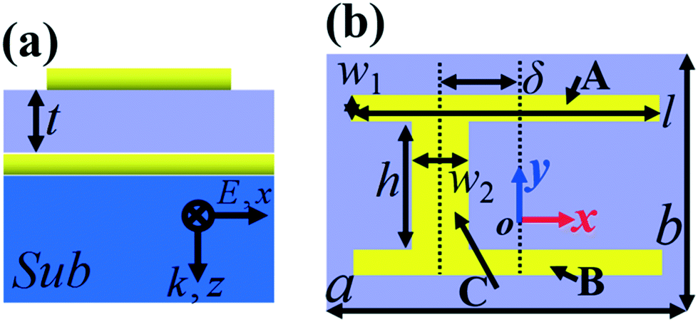 | ||
| Fig. 1 (a) Side view of the basic cell of the quad-band metamaterial absorber; (b) top view of the basic cell of the quad-band metamaterial absorber. | ||
The bottom metallic board layer of the quad-band absorption device has a thickness larger than the skin-depth of the incident terahertz beam, resulting in the transmission of the sandwich metamaterial structure being close to zero. The impedance of the sandwich metamaterial structure can be controlled by choosing different thicknesses of the separating insulating medium layer.1–3 When the sandwich metamaterial structure impedance is equal to that of air, the reflection of the sandwich metamaterial structure should be equal to zero. Simultaneously suppressed transmission and reflection provide the possibility of near-perfect absorption (or near-unity absorption). The top patterned metallic layer and bottom metallic board layer are both made of gold, which have a (frequency independent) conductivity of 4.09 × 10⁷ S m−1.
Here the optimized thickness of the separating insulating medium layer is t = 14 μm. Polyimide having a dielectric constant of 3(1 + i0.06) can be selected as the separating insulating medium layer. In order to obtain the ideal absorption effect, the numerical simulation software Lumerical FDTD Solutions (version 8.6) employing the finite-difference time-domain algorithm is utilized. A plane terahertz electromagnetic wave having a polarized direction along the X axis radiates to the sandwich metamaterial structure, and perfectly matching layers and periodic boundary conditions are respectively applied in the propagation direction of light and perpendicular to the propagation direction of light.
Results and discussion
The absorption response of the sandwich metamaterial structure is shown in Fig. 2(a). As observed, four discrete absorption peaks labeled peaks 1, 2, 3, and 4 are obtained, in which peak 1 has a resonance frequency of 1.02 THz and an absorbance of 97.57%, the resonance frequency and absorbance of peak 2 are 2.02 THz and 98.53%, respectively, peak 3 with 97.58% absorbance is localized at 2.35 THz, and the last absorption peak 4 resonates at 2.58 THz having 98.84% absorbance. According to the absorbance of each absorption peak, the average absorption intensity of the four modes can be calculated to be 98.13%, which reveals that the designed sandwich metamaterial structure can have nearly perfect absorption at four resonance frequencies. Considering that the surface (or top) structure of the sandwich metamaterial is only a metallic resonator (i.e., the asymmetric I-type resonator), this is a rather simple design method to achieve quad-band absorption compared with previous studies.10–34 Therefore, it can provide considerable possibilities in simplifying the fabrication processes of absorption devices, reducing the lattice size of the sandwich metamaterial structure, eliminating the interaction between sub-resonators, and enhancing the overall absorption capacity of the devices. In addition, the quad-band absorption performance could not be maintained when the polarization direction of the incident light wave is perpendicular to the current polarized direction (or x-axis) because of the asymmetric structure design of the top patterned metallic layer.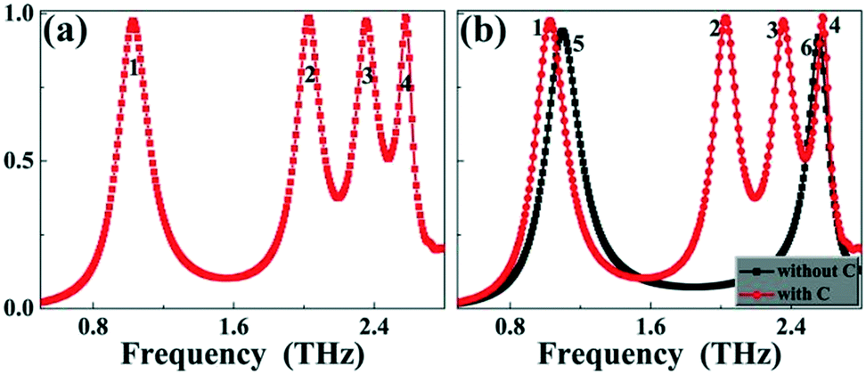 | ||
| Fig. 2 (a) Absorption response of the quad-band absorption device; (b) comparison of the absorption responses of the reduced absorber having no vertical metallic strip C and the metamaterial absorber having the vertical metallic strip C. | ||
In order to preliminarily analyze and evaluate the underlying physical origin of the quad-band absorption response, a reduced absorber formed from two horizontal metallic strips A and B lying on both layers of the insulating medium layer and metallic board is provided. That is to say, there are only two horizontal metallic strips A and B on the top layer of the reduced absorber, and there is no vertical metallic strip C. Compared with the absorber structure in Fig. 1, the reduced absorber is mainly reflected in its surface (or top) structure, and the other structure parameters (or layers) remain unchanged. The absorption response of the reduced absorber is shown as the black curve in Fig. 2(b). As observed, two resonance peaks labeled peaks 5 and 6 are realized. Peak 5 of the reduced absorber has a resonance frequency of 1.10 THz, which is close to the frequency of peak 1 in the red curve of the quad-band absorber. The resonance frequency of the second absorption peak (or peak 6) of the reduced absorber is 2.56 THz, which is approximately equal to the frequency (2.58 THz) of peak 4 in the red curve of the quad-band absorber. The comparison of the two absorption curves in Fig. 2(b) shows that the introduction of the vertical metallic strip C is a very important link in the realization of the quad-band absorption. Its introduction can induce two new absorption peaks between peaks 1 and 4, and the combination of the two induced absorption peaks and the resonance modes generated by the two horizontal metallic strips results in the quad-band absorption.
Considering the importance of vertical metallic strip C in the asymmetric I-type resonator and its important role in forming the quad-band absorption, the influence of the structure dimensions of vertical metallic strip C on the absorption performance is investigated. The structure dimension changes of the vertical metallic strip C are mainly reflected in its length w2 and width (or height) h, and the deviation value δ from the center in the basic cell. As revealed in Fig. 3(a)–(c), the resonance performance of the second and third absorption peaks (2 and 3) shows large dependence on the structure dimension variations of the vertical metallic strip C in the asymmetric I-type resonator, while the changes of the vertical metallic strip C exhibit a slight or negligible effect on the resonance performance of the first and fourth absorption peaks (1 and 4). These results are consistent with the discussion of the above paragraph that the introduction of vertical metallic strip C mainly induces two new absorption peaks 2 and 3, and the dimension changes of the vertical metallic strip itself will inevitably affect the two absorption peaks.
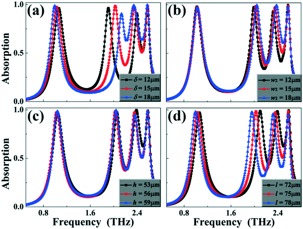 | ||
| Fig. 3 Dependence of the absorption responses on the dimension changes of the vertical metallic strip deviation value δ (a), vertical metallic strip length w2 (b), vertical metallic strip width (or height) h (c), and horizontal metallic strip length l (d). | ||
However, the influence of the dimension changes of the vertical metallic strip C on the regulation of the specific absorption peaks is different. Through comparison of Fig. 3(a)–(c), it is found that the effect of the deviation value δ on the second and third absorption peaks (2 and 3) is the most obvious and strongest, while the width (or height) h of the vertical metallic strip C exhibits the weakest and slightest influence on the two modes. This is mainly due to the strong effect of the electric field on the asymmetric I-type resonator along the X axis. For a detailed explanation, please refer to the following section for the underlying physical origin of the four absorption peaks (or the description of the corresponding field distributions in Fig. 5).
Although the dimension changes of the vertical metallic strip C mainly affect the resonance performance of the second and third absorption peaks (2 and 3), the length (l) change of the horizontal metallic strips A and B has a strong influence on all absorption peaks. As observed in Fig. 3(d), all absorption peaks of the quad-band absorption device present similar change trends that gradually decrease with the increase of length l. This kind of absorption feature is due to the fact that the resonance frequency of the metamaterial absorber is inversely proportional to the dimension of the resonator along the electric field polarized direction.1–5 In addition, we further observed that the properties of the quad-band absorption device also show dependence on the lattice periodic change. Results in Fig. 4(a) and (b) reveal that the last three absorption peaks exhibit different frequency-shift trends with the slight variations of the lattice period, while the first absorption peak 1 is nearly unchanged no matter how the lattice period changes.
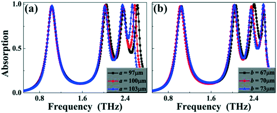 | ||
| Fig. 4 Dependence of the absorption responses on the lattice period changes of a in the X direction (a) and b in the Y direction (b). | ||
To gain insight into the underlying physical mechanism of the quad-band absorption response, the near-field distributions of the four resonance frequencies at their respective absorption maximum are provided, as shown in Fig. 5, in which (a), (b), (c) and (d) in the first row are the electric field (|E|) distributions of the four resonance frequencies at the center plane of the top metallic array, respectively. The electric field (Ez) distributions of the four resonance frequencies at the center plane of the top metallic array are presented in the second row. The third row of Fig. 5 gives the magnetic field (|Hy|) distributions of the insulating medium layer under the top metallic array along the dotted line in the first row. The fourth row in Fig. 5 gives the magnetic field (|Hy|) distributions of the insulating medium layer under the top metallic array along the solid line in the first row. As observed in Fig. 5, the near-field distributions of the four absorption peaks are different.
 | ||
| Fig. 5 Near-field distributions of the perfect absorption peaks at 1.02 THz, 2.02 THz, 2.35 THz, and 2.58 THz, in which the first column is the field distributions of peak 1, and the second, third and fourth columns are respectively the field distributions of peaks 2, 3, and 4. (a)–(d) are electric field distributions of peaks 1, 2, 3, and 4 at the center plane of the top metallic array, respectively. (e)–(h) are electric field (Ez) distributions of peaks 1, 2, 3, and 4 at the center plane of the top metallic array, respectively. (i) and (n) are magnetic field (|Hy|) distributions of peak 1 at the insulating medium layer under the top metallic array along the upper and middle solid lines, respectively. (j) and (m) are magnetic field (|Hy|) distributions of the peak 2 at the insulating medium layer under the top metallic array along the upper and middle solid lines, respectively. (k) and (o) are magnetic field (|Hy|) distributions of the peak 3 at the insulating medium layer under the top metallic array along the upper and middle solid lines, respectively. (l) and (p) are magnetic field (|Hy|) distributions of the peak 4 at the insulating medium layer under the top metallic array along the upper and middle solid lines, respectively. | ||
In particular terms, for absorption peak 1 at 1.02 THz, we observed that its electric fields (|E| and Ez) in Fig. 5(a) and (e) are both chiefly focused on both sides of the horizontal metallic strips, while negligible field distributions are found at the edges of the vertical metallic strip. The near-field distributions of absorption peak 1 in Fig. 5(i) and (n) further reveal that most of its magnetic fields having only one aggregation area are localized at the insulating medium layer under the horizontal metallic strip. The near-field distribution characteristics of absorption peak 1 in Fig. 5(a), (i) and (n) indicate that this absorption mode is mostly related to the fundamental mode (or the first-order) localized resonance response of the two horizontal metallic strips and has nothing to do with the vertical metallic strip. This is why absorption peak 1 has a slight (or negligible) effect regardless of the changes of the vertical metallic strip and lattice period.
For absorption peak 4 at 2.58 THz, similar near-field distribution features are obtained as shown in Fig. 5(d) and (h) where its electric fields (|E| and Ez) are obviously enhanced (or have a large proportion) at both sides of the horizontal metallic strips, while a rather small proportion of the electric fields is concentrated on the edges of the vertical metallic strip. Furthermore, unlike the magnetic field (|Hy|) distributions of absorption peak 1 in Fig. 5(i) and (n), the magnetic field (|Hy|) distributions of absorption peak 4 in Fig. 5(l) and (p) have three strong (or obvious) enhancement areas, which reveal that absorption peak 4 should be derived from the third-order mode in the higher-order resonance effect of the horizontal metallic strips. It should be noted that the resonance frequencies of absorption peaks 1 and 4 also imply the formation mechanisms of the two absorption modes. Absorption peak 4 has a frequency of 2.58 THz, which is 2.53 times and nearly 3 times that of absorption peak 1. The frequency of the third-order resonance response of an ideal metallic resonator is three times that of the first-order resonance effect. However, it is usually less than three times under normal cases, which is mainly caused by the influence and disturbance of other resonators, such as the vertical metallic strip C here.
For absorption peaks 2 and 3, it is found that their electric fields have similar enhancement features that are majorly focused on the horizontal metallic strips. However, unlike the electric field distribution characteristics of absorption peaks 1 and 4, their electric fields are not concentrated on the edges of the entire horizontal metallic strips, but distributed at the edges of a specific part of the horizontal metallic strips. For example, for absorption peak 2 at 2.02 THz, its electric fields in Fig. 5(b) have a strong enhancement effect at the left edges of the horizontal metallic strips. Meanwhile, a strong near-field enhancement effect can be observed at the left edges of the horizontal metallic strips and the right side of the vertical metallic strip, see Fig. 5(f). The magnetic field distribution of absorption peak 1 having only one aggregation area is observed in the left part of the insulating medium layer under the left part of the horizontal metallic strip along the dotted line. It is demonstrated that absorption peak 2 is mainly caused by the fundamental mode resonance response of the left part of the horizontal metallic strips. Combining the electric and magnetic field distributions of absorption peak 3 in Fig. 5(c), (g), (k) and (o), it can be inferred that this absorption mode mainly results from the fundamental mode resonance response of the right part of the horizontal metallic strips. In other words, the introduction of the vertical metallic strip in the asymmetric I-type resonator can divide the horizontal metallic strips into two different parts, with each part corresponding to a specific absorption peak. Combining the fundamental mode and the third-order resonance response of the horizontal metallic strips and the two induced absorption peaks generated by the introduction of the vertical metallic strip provides the ability to achieve the perfect absorption in the four frequency bands. This in turn can explain why the dimension changes of the vertical metallic strip have a strong influence on the second and third absorption peaks, and have a slight (or negligible) influence on the other two absorption peaks, see Fig. 3.
Potential applications
Because the vertical metallic strip C in the asymmetric I-type resonator plays an important role in the generation of the second and third absorption peaks as well as in the realization of the quad-band absorption, its existence or not can directly determine the number of absorption peaks in the designed sandwich metamaterial structure. It can be predicted that the absorption performance of the metamaterial absorber, especially the number of absorption peaks, could be adjustable when the vertical metallic strip C is replaced with a material having the features of changing from low conductivity to high conductivity. The photosensitive silicon material is a kind of suitable material that can realize the transition from low conductivity to high conductivity through external stimulation such as pump light intensity.35–37 With the increase of external stimulation intensity, the conductivity of photosensitive silicon can gradually increase, thus realizing the transformation from dielectric to metallic.35–37 We here give an adjustable metamaterial absorber using photosensitive silicon instead of the vertical metallic strip in the original asymmetric I-type resonator. The top view of the adjustable metamaterial absorber is given in Fig. 6(a), in which the photosensitive silicon is shown in the red area. What needs to be clear is that only the vertical metallic strip is replaced with the photosensitive silicon, while the other structure parameters, material properties, model code and its boundary conditions are all unchanged.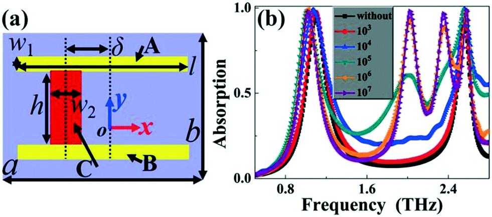 | ||
| Fig. 6 (a) Top view of the multi-band metamaterial absorber having adjustable absorption peaks; (b) dependence of the absorption responses on the conductivity changes of the photosensitive silicon. | ||
Fig. 6(b) provides the absorption response of the adjustable metamaterial absorber. It can be seen from the black and red curves that the adjustable absorption device has only two absorption peaks when the photosensitive silicon is not used or has low conductivity for presenting the dielectric property. With the increase of the conductivity of the photosensitive silicon, two new resonance bands gradually appear between the two perfect absorption peaks. The two new resonance bands can reach near-perfect absorbance when the photosensitive silicon shows the metallic property, see the purple curve of Fig. 6(b). The quad-band absorption can be achieved by combining the two new absorption peaks with the original two nearly invariable absorption peaks. This shows that the number of absorption peaks can be flexibly adjusted from the initial dual-band to the quad-band by gradually changing the properties of photosensitive silicon for realizing the transformation from low conductivity to high conductivity. This type of resonance device with an adjustable number of absorption peaks could provide a wide range of application prospects in many technology-related areas.
In fact, when the patterned metallic structure on the top layer of the metamaterial absorber is covered with a layer of covering (or analyte), the sensing and detection performance of the designed metamaterial absorber can be further explored, and the influence of sensing spectral performance on the changes of the refractive index and thickness of the analyte could also be explored.38–43 Moreover, considering the strong electric field distribution (or the so-called “hot spot” effect) near the metallic pattern structure, it is possible for the designed resonance device to be used in SERS detection, sample composition identification or trace qualitative analysis of hazardous substances.44–46
Conclusions
In conclusion, a multi-band metamaterial absorber operating in the terahertz frequency domain using the structure design of an asymmetric I-type resonator (formed from two horizontal metallic strips and a vertical metallic strip) and an insulating dielectric layer lying on a metallic board is suggested in this paper. Near-perfect absorption at four discrete resonance frequencies is achieved. The combination effect of the four resonance modes originating from different localized responses of the asymmetric I-type resonator results in the quad-band absorption. Results further demonstrate that changing the dimensions of the asymmetric I-type resonator, especially the dimensions of the vertical metallic strip, has great ability to control the resonance performance of the four absorption peaks, including the resonance frequencies, absorbance and the number of absorption peaks. Compared with previous methods for achieving multi-band absorption, the multi-band device designed here has the advantages of simple structure design, small lattice dimension, easy construction, convenient regulation, etc. Considering the obvious influence of the structure dimensions on the absorption performance, a new type of metamaterial absorber with adjustable absorption peaks is designed by introducing photosensitive silicon to replace the vertical metallic strip in the original asymmetric I-type resonator. The material properties of the photosensitive silicon can be changed from low conductivity to high conductivity through external stimulation, thus the metamaterial absorber has the ability to adjust the number of absorption peaks from the dual-band to the quad-band. The multi-band terahertz metamaterial absorber proposed here could have great application potential in many fields, such as thermal imaging, Raman enhancement, sensing and detection, etc.Author contributions
Ben-Xin Wang: conceptualization, data curation, formal analysis, methodology, funding acquisition, project administration, writing – review & editing; Yangkuan Wu: data curation, investigation, validation, resources, writing – original draft; Wei Xu: data curation, formal analysis, validation; Liming Lu: data curation, validation; Fuwei Pi: supervision, writing – review & editing.Conflicts of interest
There are no conflicts of interest to declare.Acknowledgements
This research was funded by the National Natural Science Foundation of China (62105128) and the China Postdoctoral Science Foundation (2019M651692).References
- C. M. Watts, X. Liu and W. J. Padilla, Metamaterial electromagnetic wave absorbers, Adv. Mater., 2012, 24, OP98 CAS.
- Y. Cui, Y. He, Y. Jin, F. Ding, L. Yang, Y. Ye, S. Zhong, Y. Lin and S. He, Plasmonic and metamaterial structures as electromagnetic absorbers, Laser Photonics Rev., 2014, 8, 495 CrossRef CAS.
- N. I. Landy, S. Sajuyigbe, J. J. Mock, D. R. Smith and W. J. Padilla, Perfect metamaterial absorber, Phys. Rev. Lett., 2008, 100, 207402 CrossRef CAS PubMed.
- D. Wu, R. Li, Y. Liu, Z. Yu, L. Yu, L. Chen, C. Liu, R. Ma and H. Ye, Ultra-narrow band perfect absorber and its application as plasmonic sensor in the visible region, Nanoscale Res. Lett., 2017, 12, 427 CrossRef PubMed.
- S. Ogawa and M. Kimata, Metal-insulator-metal-based plasmonic metamaterial absorbers at visible and infrared wavelengths: A review, Materials, 2018, 11, 458 CrossRef PubMed.
- P. Yu, L. V. Besteiro, J. Wu, Y. Huang, Y. Wang, A. O. Govorov and Z. Wang, Metamaterial perfect absorber with unabated size-independent absorption, Opt. Express, 2018, 26, 20471 CrossRef CAS PubMed.
- J. Schalch, G. Duan, X. Zhao, X. Zhang and R. D. Averitt, Terahertz metamaterial perfect absorber with continuously tunable air spacer layer, Appl. Phys. Lett., 2018, 113, 061113 CrossRef.
- H. Hajian, A. Ghobadi, B. Butun and E. Ozbay, Active metamaterial nearly perfect light absorbers: A review, J. Opt. Soc. Am. B, 2019, 36, F131 CrossRef CAS.
- O. Rance, A. C. Lepage, X. Begaud, K. Elis and N. Capet, Oblique wide-angle multi-sector metamaterial absorber for space applications, Appl. Sci., 2019, 9, 3425 CrossRef CAS.
- M. D. Astorino, F. Frezza and N. Tedeschi, Ultra-thin narrow-band, complementary narrow-band, and dual-band metamaterial absorbers for applications in the THz regime, J. Appl. Phys., 2017, 121, 063103 CrossRef.
- J. Zhang, J. Tian and L. Li, A dual-band tunable metamaterial near-unity absorber composed of periodic cross and disk graphene arrays, IEEE Photonics J., 2018, 10, 4800512 Search PubMed.
- S. Ji, C. Jiang, J. Zhao, J. Yang, J. Wang and H. Dai, An ultra-thin dual-band wide-angle polarization-insensitive metamaterial absorber with near-unity absorbance, Curr. Appl. Phys., 2019, 19, 1164 CrossRef.
- C. Cen, Y. Zhang, X. Chen, H. Yang, Z. Yi, W. Yao, Y. Tang, Y. Yi, J. Wang and P. Wu, A dual-band metamaterial absorber for graphene surface plasmon resonance at terahertz frequency, Phys. E, 2020, 117, 113840 CrossRef CAS.
- Z. Yin, Y. Lu, T. Xia, W. Lai, J. Yang, H. Lu and G. Deng, Electrically tunable terahertz dual-band metamaterial absorber based on a liquid crystal, RSC Adv., 2018, 8, 4197 RSC.
- J. Song, L. Wang, M. Li and J. Dong, A dual-band metamaterial absorber with adjacent absorption peaks, J. Phys. D: Appl. Phys., 2018, 51, 385105 CrossRef.
- N. Mishra, D. K. Choudhary, R. Chowdhury, K. Kumari and R. K. Chaudhary, An investigation on compact ultra-thin triple-band polarization independent metamaterial absorber for microwave frequency applications, IEEE Access, 2017, 5, 4370 Search PubMed.
- R. Wang, L. Li, J. Liu, F. Yan, F. Tian, H. Tian, J. Zhang and W. Sun, Triple-band tunable perfect terahertz metamaterial absorber with liquid crystal, Opt. Express, 2017, 25, 32280 CrossRef CAS.
- B. X. Wang, C. Tang, Q. Niu, Y. He and T. Chen, Design of narrow discrete distances of dual-/triple-band terahertz metamaterial absorbers, Nanoscale Res. Lett., 2019, 14, 64 CrossRef PubMed.
- B. X. Khuyen, B. S. Tung, Y. J. Kim, J. S. Hwang, K. W. Kim, J. Y. Rhee, V. D. Lam, Y. H. Kim and Y. P. Lee, Ultra-subwavelength thickness for dual/triple-band metamaterial absorber at very low frequency, Sci. Rep., 2018, 8, 11632 CrossRef PubMed.
- X. Zeng, M. Gao, L. Zhang, G. Wan and B. Hu, Design of a triple-band metamaterial absorber using equivalent circuit model and interference theory, Microw. Opt. Technol. Lett., 2018, 60, 1676 CrossRef.
- J. W. Park, P. V. Tuong, J. Y. Rhee, K. W. Kim, W. H. Jang, E. H. Choi, L. Y. Chen and Y. P. Lee, Multi-band metamaterial absorber based on the arrangement of donut-type resonators, Opt. Express, 2013, 21, 9691 CrossRef PubMed.
- M. Agarwal, A. K. Behera and M. K. Meshram, Wide-angle quad-band polarisation-insensitive metamaterial absorber, Electron. Lett., 2016, 52, 340 CrossRef CAS.
- Y. H. Ren, J. Ding, C. J. Guo, Y. Qu and Y. C. Song, Design of a quad-band wide-angle microwave metamaterial absorber, J. Electron. Mater., 2017, 46, 370 CrossRef CAS.
- A. Sarkhel and S. R. B. Chaudhuri, Compact quad-band polarization-insensitive ultrathin metamaterial absorber with wide angle stability, IEEE Antennas Wirel. Propag. Lett., 2018, 16, 3240 Search PubMed.
- H. S. Singh, Super compact ultrathin quad-band with wide angle stability polarization independent metamaterial absorber, Microw. Opt. Technol. Lett., 2020, 62, 718 CrossRef.
- S. Kalraiya, R. K. Chaudhary, R. K. Gangwar and M. A. Abdalla, Compact quad-band polarization independent metamaterial absorber using circular/square metallic ring resonator, Mater. Res. Express, 2019, 6, 055812 CrossRef CAS.
- S. Liu, J. Zhuge, S. Ma, H. Chen, D. Bao, Q. He, L. Zhou and T. J. Cui, A bi-layered quad-band metamaterial absorber at terahertz frequencies, J. Appl. Phys., 2015, 118, 245304 CrossRef.
- S. Shang, S. Yang, L. Tao, L. Yang and H. Cao, Ultrathin triple-band polarization-iinsensitive wide-angle compact metamaterial absorber, AIP Adv., 2016, 6, 075203 CrossRef.
- K. P. Kaur and T. Upadhyaya, Wide-angle and polarisation-independent triple-band dual-layer microwave metamaterial absorber, IET Microw. Antennas Propag., 2018, 12, 1428 CrossRef.
- T. L. Pham, H. T. Dinh, D. H. Le, X. K. Bui, S. T. Bui, H. L. Dang, A. D. Phan, D. T. Le and D. L. Vu, Dual-band isotropic metamaterial absorber based on near-field interaction in the Ku band, Curr. Appl. Phys., 2020, 20, 331 CrossRef.
- Z. Su, J. Yin and X. Zhao, Terahertz dual-band metamaterial absorber based on graphene/MgF2 multilayer structures, Opt. Express, 2015, 23, 1679 CrossRef CAS PubMed.
- P. Munaga, S. Bhattacharyya, S. Ghosh and K. V. Srivastava, An ultra-thin compact polarization-independent hexa-band metamaterial absorber, Appl. Phys. A: Mater. Sci. Process., 2018, 124, 331 CrossRef.
- F. Bagci and F. Medina, Design of a wide-angle, polarization-insensitive, dual-band metamaterial-inspired absorber with the aid of equivalent circuit model, J. Comput. Electron., 2017, 16, 913 CrossRef CAS.
- S. Asgari, N. Sharifi and N. Granpayeh, Active tunable terahertz micro-electromachanical metamaterial absorber, J. Micromech. Microeng., 2019, 29, 045010 CrossRef CAS.
- N. H. Shen, M. Kafesaki, T. Koschny, L. Zhang, E. N. Economou and C. M. Soukoulis, Broadband blueshift tunable metamaterials and dual-band switches, Phys. Rev. B: Condens. Matter Mater. Phys., 2009, 79, 161102 CrossRef.
- H. T. Chen, J. F. Ohara, A. K. Azad, A. J. Taylor, R. D. Averitt, D. B. Shrekenhamer and W. J. Padilla, Experimental demonstration of frequency-agile terahertz metamaterial, Nat. Photonics, 2008, 2, 295 CrossRef CAS.
- K. Ren, Y. M. He, X. B. Ren, Y. Zhang, Q. Han, L. D. Wang and M. J. Xu, Dynamically tunable multi-channel and polarization-independent electromagnetically induced transparency in terahertz metasurfaces, J. Phys. D: Appl. Phys., 2020, 53, 135107 CrossRef CAS.
- L. Cong, S. Tan, R. Yahiaoui, F. Yan, W. Zhang and R. Singh, Experimental demonstration of ultrasensitive sensing with terahertz metamaterial absorbers: A comparison with the metasurfaces, Appl. Phys. Lett., 2015, 106, 031107 CrossRef.
- B. X. Wang, G. Z. Wang and T. Sang, Simple design of novel triple-band terahertz metamaterial absorber for sensing application, J. Phys. D: Appl. Phys., 2016, 49, 165307 CrossRef.
- X. Hu, G. Xu, L. Wen, H. Wang, Y. Zhao, Y. Zhang, D. R. S. Cumming and Q. Chen, Metamaterial absorber integrated microfluidic terahertz sensors, Laser Photonics Rev., 2016, 10, 962 CrossRef CAS.
- B. X. Wang, Y. He, P. Lou and W. Xing, Design of a dual-band terahertz metamaterial absorber using two identical square patches for sensing application, Nanoscale Adv., 2020, 2, 763 RSC.
- B. X. Wang, Y. He, P. Lou and H. Zhu, Multi-band terahertz superabsorbers based on perforated square-patch metamaterials, Nanoscale Adv., 2021, 3, 455 RSC.
- Y. Li, X. Chen, F. Hu, D. Li, H. Teng, Q. Rong, W. Zhang, J. Han and H. Liang, Four resonators based high sensitive terahertz metamaterial biosensor used for measuring concentration of protein, J. Phys. D: Appl. Phys., 2019, 52, 095105 CrossRef.
- S. Kasani, K. Curtin and N. Wu, A review of 2D and 3D plasmonic nanostructure array patterns: fabrication, light management and sensing applications, Nanophotonics, 2019, 8, 2065 CAS.
- C. Zong, M. Xu, L. J. Xu, T. Wei, X. Ma, X. S. Zheng, R. Hu and B. Ren, Surface-enhanced Raman spectroscopy for bioanalysis: Reliability and challenges, Chem. Rev., 2018, 118, 4946 CrossRef CAS PubMed.
- N. Jiang, Z. Zhuo and J. Wang, Action plasmonics: Principles, structures, and applications, Chem. Rev., 2018, 118, 3054 CrossRef CAS PubMed.
| This journal is © The Royal Society of Chemistry 2022 |